EP3723148A1 - Three-dimensional capacitive structures and their manufacturing methods - Google Patents
Three-dimensional capacitive structures and their manufacturing methods Download PDFInfo
- Publication number
- EP3723148A1 EP3723148A1 EP19305457.4A EP19305457A EP3723148A1 EP 3723148 A1 EP3723148 A1 EP 3723148A1 EP 19305457 A EP19305457 A EP 19305457A EP 3723148 A1 EP3723148 A1 EP 3723148A1
- Authority
- EP
- European Patent Office
- Prior art keywords
- pores
- capacitive
- layer
- anodization
- anodic oxide
- Prior art date
- Legal status (The legal status is an assumption and is not a legal conclusion. Google has not performed a legal analysis and makes no representation as to the accuracy of the status listed.)
- Pending
Links
Images

Classifications
-
- H—ELECTRICITY
- H10—SEMICONDUCTOR DEVICES; ELECTRIC SOLID-STATE DEVICES NOT OTHERWISE PROVIDED FOR
- H10D—INORGANIC ELECTRIC SEMICONDUCTOR DEVICES
- H10D1/00—Resistors, capacitors or inductors
- H10D1/01—Manufacture or treatment
- H10D1/041—Manufacture or treatment of capacitors having no potential barriers
- H10D1/043—Manufacture or treatment of capacitors having no potential barriers using patterning processes to form electrode extensions, e.g. etching
-
- H—ELECTRICITY
- H01—ELECTRIC ELEMENTS
- H01G—CAPACITORS; CAPACITORS, RECTIFIERS, DETECTORS, SWITCHING DEVICES, LIGHT-SENSITIVE OR TEMPERATURE-SENSITIVE DEVICES OF THE ELECTROLYTIC TYPE
- H01G4/00—Fixed capacitors; Processes of their manufacture
- H01G4/002—Details
- H01G4/005—Electrodes
- H01G4/008—Selection of materials
-
- H—ELECTRICITY
- H01—ELECTRIC ELEMENTS
- H01G—CAPACITORS; CAPACITORS, RECTIFIERS, DETECTORS, SWITCHING DEVICES, LIGHT-SENSITIVE OR TEMPERATURE-SENSITIVE DEVICES OF THE ELECTROLYTIC TYPE
- H01G4/00—Fixed capacitors; Processes of their manufacture
- H01G4/002—Details
- H01G4/005—Electrodes
- H01G4/012—Form of non-self-supporting electrodes
-
- H—ELECTRICITY
- H01—ELECTRIC ELEMENTS
- H01G—CAPACITORS; CAPACITORS, RECTIFIERS, DETECTORS, SWITCHING DEVICES, LIGHT-SENSITIVE OR TEMPERATURE-SENSITIVE DEVICES OF THE ELECTROLYTIC TYPE
- H01G4/00—Fixed capacitors; Processes of their manufacture
- H01G4/002—Details
- H01G4/018—Dielectrics
- H01G4/06—Solid dielectrics
- H01G4/08—Inorganic dielectrics
- H01G4/10—Metal-oxide dielectrics
-
- H—ELECTRICITY
- H01—ELECTRIC ELEMENTS
- H01G—CAPACITORS; CAPACITORS, RECTIFIERS, DETECTORS, SWITCHING DEVICES, LIGHT-SENSITIVE OR TEMPERATURE-SENSITIVE DEVICES OF THE ELECTROLYTIC TYPE
- H01G4/00—Fixed capacitors; Processes of their manufacture
- H01G4/002—Details
- H01G4/018—Dielectrics
- H01G4/06—Solid dielectrics
- H01G4/08—Inorganic dielectrics
- H01G4/12—Ceramic dielectrics
- H01G4/1272—Semiconductive ceramic capacitors
-
- H—ELECTRICITY
- H01—ELECTRIC ELEMENTS
- H01G—CAPACITORS; CAPACITORS, RECTIFIERS, DETECTORS, SWITCHING DEVICES, LIGHT-SENSITIVE OR TEMPERATURE-SENSITIVE DEVICES OF THE ELECTROLYTIC TYPE
- H01G4/00—Fixed capacitors; Processes of their manufacture
- H01G4/30—Stacked capacitors
- H01G4/306—Stacked capacitors made by thin film techniques
-
- H—ELECTRICITY
- H01—ELECTRIC ELEMENTS
- H01G—CAPACITORS; CAPACITORS, RECTIFIERS, DETECTORS, SWITCHING DEVICES, LIGHT-SENSITIVE OR TEMPERATURE-SENSITIVE DEVICES OF THE ELECTROLYTIC TYPE
- H01G4/00—Fixed capacitors; Processes of their manufacture
- H01G4/33—Thin- or thick-film capacitors (thin- or thick-film circuits; capacitors without a potential-jump or surface barrier specially adapted for integrated circuits, details thereof, multistep manufacturing processes therefor)
-
- H—ELECTRICITY
- H10—SEMICONDUCTOR DEVICES; ELECTRIC SOLID-STATE DEVICES NOT OTHERWISE PROVIDED FOR
- H10D—INORGANIC ELECTRIC SEMICONDUCTOR DEVICES
- H10D1/00—Resistors, capacitors or inductors
- H10D1/60—Capacitors
- H10D1/68—Capacitors having no potential barriers
- H10D1/692—Electrodes
- H10D1/711—Electrodes having non-planar surfaces, e.g. formed by texturisation
- H10D1/714—Electrodes having non-planar surfaces, e.g. formed by texturisation having horizontal extensions
-
- H—ELECTRICITY
- H10—SEMICONDUCTOR DEVICES; ELECTRIC SOLID-STATE DEVICES NOT OTHERWISE PROVIDED FOR
- H10D—INORGANIC ELECTRIC SEMICONDUCTOR DEVICES
- H10D1/00—Resistors, capacitors or inductors
- H10D1/60—Capacitors
- H10D1/68—Capacitors having no potential barriers
- H10D1/692—Electrodes
- H10D1/711—Electrodes having non-planar surfaces, e.g. formed by texturisation
- H10D1/716—Electrodes having non-planar surfaces, e.g. formed by texturisation having vertical extensions
Definitions
- the present invention relates to the field of electrical/electronic devices and to methods of their fabrication. More particularly, the invention relates to devices that incorporate three-dimensional capacitive structures, and to methods of manufacturing such devices.
- Another approach that has been proposed for providing a high-density capacitor consists in creating a porous region of anodic metal oxide (e.g. anodic aluminium oxide, AAO) and then depositing a single or repeated Metal-Insulator-Metal (MIM) stack structure conformally over the porous region, such that the MIM layers follow the contours of the pores and have a resultant large surface area.
- anodic metal oxide e.g. anodic aluminium oxide, AAO
- MIM Metal-Insulator-Metal
- a metal layer for example, an aluminium layer
- an anodization process is performed on a selected region of the metal layer to create there a high density of uniform, self-assembled trenches, or "pores".
- FIG.1A illustrates a template of the above-described kind formed by anodization.
- porous anodic oxide is an effective technique to enhance the surface area of the electrodes, but there can be a problem in achieving a sufficiently-low Equivalent Series Resistance (ESR) of the fabricated capacitive structure.
- ESR Equivalent Series Resistance
- WO2015/063420 proposes to remove the anodic oxide layer at the bottoms of the pores so that the interior of each pore can be brought into communication with a stack of electrically conductive layers provided at the substrate side. In this way, the lower layer of the MIM stack in each pore is connected, on the substrate side, to the lower layer of the MIM stack in an adjacent pore, lowering the ESR of the overall structure.
- Fig.1B is a simplified diagram illustrating a capacitive structure 50 of the general kind described in WO2015/063420 .
- a region 52a of porous AAO is formed in an aluminium layer 52 provided on a silicon substrate 51. More specifically, the aluminium layer 52 is formed on a stack of layers comprising: a lower electrically-conductive layer 58, and an upper layer 59 which is resistant to anodization/anodic etching.
- the pores in the anodic oxide region 52a are open at the substrate side. Accordingly, a first metal layer 53 that is formed conformally over the porous region 52a comes into contact with the underlying stack of layers 58, 59.
- the anodization-resistant layer 59 has sufficient electrical conductivity to enable a good electrical connection to be made, at the bottoms of the pores, between the electrically-conductive layer 58 and the first metal layer 53.
- a dielectric layer 54 and second electrically conductive layer 55 form, with the first conductive layer 53, a MIM stack which functions as a capacitive element.
- a first terminal of the capacitive element is formed on the side 56 remote from the substrate by making a connection to the second conductive layer 55.
- the second terminal of the capacitive element may be formed on either side of the structure (i.e. on the side 56 or on the substrate side) by making a connection to the electrically conductive layer 58.
- a crack labelled C is indicated schematically in Fig.1B
- Fig.1C is an image, obtained by scanning electron microscopy, showing a crack in an anodization-resistant layer made of tungsten (W).
- W tungsten
- the present invention has been made in the light of the above-described problems.
- the present invention provides a capacitive structure comprising:
- the functional portion of the capacitive stack which contributes to the capacitance of the finished structure is not in direct contact with the portion of the anodization-resistant layer where cracks may arise. Accordingly, the negative effects of such cracks are reduced. More particularly, undesired leakage current is reduced and the electrical characteristics of the finished structure are improved, thereby the yield of the process used for manufacturing the structures can be improved. In view of the yield improvement, it becomes feasible to make use of relatively thicker layers for the anodization-resistant layer and the electrically-conductive interconnection layer, which facilitates the achievement of a low value of ESR at the same time as a high capacitance density.
- anodization-resistant layer which is 600 nm thick and an interconnection layer which is 3 ⁇ m thick.
- interconnection layer which is 3 ⁇ m thick.
- the target properties of the capacitive structure can be obtained more reliably, achieving a capacitive component having improved reliability and increased lifetime.
- the aspect ratio of the pores is high and, at the bottoms of the pores, it is difficult to deposit the layers of the capacitive stack to the desired thickness. This can adversely affect the ESR and breakdown voltage of the overall capacitive structure.
- the functional portion of the capacitive stack above the position where the pore diameter is reduced, non-uniformity in the thickness of the layers of the capacitive stack in the vicinity of the bottoms of the pores has reduced effect (potentially, negligible effect) on the performance of the overall capacitive structure.
- the first portion of the capacitive stack of layers, which contributes to the capacitance of the capacitive structure is located in portions of the pores that are between the restricted-diameter position and the surface of the anodic oxide remote from the substrate.
- the first conductive layer of the stack is formed conformally over the pores in the porous region, the first insulator layer is formed on the first conductive layer, the second conductive layer is formed on the first insulator layer, and the second conductive layer extends into the pores no further than the position of reduced pore diameter. Because the second conductive layer does not extend beyond the reduced-diameter position in the pores, the functional portion of the capacitive structure (including both of the first and second conductive layers as well as the interposed insulating layer) is located between the reduced-diameter position in the pores and the surface of the anodic oxide region that is remote from the substrate.
- the following relationship is set: D ⁇ 2 T c 1 + T i 1 where D is the diameter of the pore at the restricted-diameter location, T c1 is the thickness of the first conductive layer, and T i1 is the thickness of the first insulator layer.
- the second conductive layer can be prevented from extending into the pores beyond the position of reduced pore diameter.
- the position of reduced-diameter of the pores is located at a distance of 10-300 nm from the bottom of the pores.
- the anodization-resistant layer is made of tungsten.
- the anodization-resistant layer may be made of other materials including, but not limited to, Ti, Ta, Hf and Nd.
- the average thickness of the anodization-resistant layer is in the range 10 nm - 1 ⁇ m.
- the anodic oxide is anodic aluminium oxide.
- the porous material may be made of other substances including, but not limited to porous anodized Ti, Si, Ta or Zr.
- the present invention still further provides a method of fabricating a capacitive structure, comprising:
- the inventors have studied the potential origin of the cracks that can occur in the anodization-resistant layer. Their studies suggest that such cracks may arise because there are weak points in the anodization-resistant layer 59 in the vicinity of the bottoms of the pores. The current understanding of the origin of such weak points is explained below.
- an anodization process is performed to create the pores of the porous anodic oxide region 52a, and the anodization process is continued until the bottoms of the pores are opened, to a sufficient degree, onto the upper layer 59.
- the anodization process which opens the pore bottoms there is a certain degree of migration of atoms of the material (e.g. tungsten, W) forming the anodization-resistant layer 59 at regions which underlie the pores, and undesired small regions of oxide (e.g. tungsten oxide) are formed.
- the material e.g. tungsten, W
- undesired small regions of oxide e.g. tungsten oxide
- this undesired oxide is removed, typically by an etching process. It is believed that this migration of atoms in the material forming the anodization-resistant layer 59 results in weak points in the anodization layer 59, and a propensity to cracking.
- Embodiments of the invention exploit the fact that the pores in the anodic oxide may have a position of reduced diameter, this position being towards the bottoms of the pores.
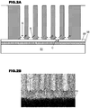
- Fig.2A the pores formed by the manufacturing method described above with reference to Fig.1B do not have a uniform cross-sectional area along the entirety of their length. Instead, they have an unusual and characteristic shape as can be seen in Fig.2B which is an enlarged view of the bottoms of a set of pores, produced by scanning electron micrography.
- the capacitive stack is formed in the pores of the anodic oxide region so that, in at least 1% of the pores, a functional portion F of the capacitive stack, which determines the capacitance of the overall structure, is located above the reduced-diameter position in the pores ("above” meaning further from the substrate than the position of reduced pore diameter).
- a functional portion F of the capacitive stack which determines the capacitance of the overall structure.
- first conductive layer and first insulating layer of the capacitive stack have thicknesses, relative to the diameter of the reduced-diameter location in the pores, which mean that these layers clog the bottom of the pores and the second conductive layer does not pass through the "throat" of the reduced-diameter location.
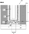
- a capacitive stack according to an embodiment of the invention will now be described with reference to Fig.3 , and an example embodiment of a method to fabricate this structure will be described with reference to Fig.4 .
- a capacitive structure 150 includes a region 152a of porous anodic oxide formed on a stack of layers comprising: a lower electrically-conductive layer 158, and an upper layer 159 which is resistant to anodization/anodic etching.
- the stack of layers 158, 159 may be provided on a substrate (not shown), for example, in a case where the capacitive structure is being integrated with other electrical components, and/or in a case where a substrate can increase the strength of the overall structure.
- the substrate may itself serve as an interconnection layer to electrically-connect the lowermost conductive layer at the bottom of one pore to those in neighbouring pores. Accordingly, it may be possible in such cases to do without a separate layer 158.
- the pores in the anodic oxide region 152a are open at the substrate side and have a position P where the diameter of the pore is reduced. The reduced-diameter position in the pore has a diameter designated D.
- a first electrically-conductive layer 153 is formed conformally over the porous region 152a and comes into contact with the underlying stack of layers 158, 159.
- the anodization-resistant layer 159 has sufficient electrical conductivity to enable a good electrical connection to be made, at the bottoms of the pores, between the electrically-conductive layer 158 and the first conductive layer 153.
- the first conductive layer 153 is coated on the walls of the pore and follows the generally-cylindrical shape along the majority of the pore's length, as well as following the shape of the pore wall at the bottom of the pore.
- the first conductive layer 153 passes through the reduced-diameter throat of the pore at position P and makes contact with the anodization-resistant layer 159.
- Fig.3 illustrates a single pore in a region of porous anodic oxide but it will be understood that, in practice, the first conductive layer 153 will conformally coat the walls of a group of adjacent pores in the region of porous anodic oxide.
- a first insulating layer 154 is provided on the first conductive layer 153 and generally follows the shape of the underlying first conductive layer 153.
- the thicknesses of the first conductive layer 153 and the first insulating layer 154 are such that the reduced-diameter throat of the pore is closed off. More particularly, the first insulating layer 154 coating opposing surfaces of the pore makes contact with itself at a location just above the reduced-diameter position P in the pore. So, the inner surface of the first insulating layer 154 defines a generally cylindrical bore whose diameter is substantially constant along its length.
- a second electrically-conductive layer 155 is provided on the inner surface of the first insulating layer 154. The second conductive layer 155 does not pass through the reduced-diameter throat of the pore; instead it conformally follows the shape of the inner surface of the first insulating layer 154 and, thus, it has a regular shape.
- the second electrically conductive layer 155 forms a capacitive stack with the first conductive layer 153 and the intervening first insulating layer 154.
- a capacitive stack having layers of these kinds is often referred to as a MIM stack (from "metal-insulator-metal") even though the conductive layers may be formed of materials which are not pure metals.
- the second conductive layer 155 is not present below the position P where the pore has reduced diameter. It is only the portion F of the stacked layers, where all three of the first conductive layer, first insulating layer and second conductive layer are present, that is operational as a capacitor. However, the lower section of the first conductive layer, which coats the pore walls at, and underneath, the position P having reduced pore-diameter, makes electrical contact between the functional portion F of the capacitive stack and the underlying interconnection layers 158, 159.
- the capacitive stack may be formed of extra layers additional to the layers 153, 154, 155.
- the capacitive stack may be a MIMIM stack, an MIMIMIM stack, and so on.
- the "throat" at the reduced-diameter location in the pores becomes closed off between the first and second MIM structures.
- the conductive layers are very thin (e.g. approximately 5 nm or less) then it may be just the topmost conductive layer that fails to pass through the reduced-diameter location.
- the first conductive layer may be made of TiN.
- the thickness of the first conductive layer 153 is in the range 1 nm-30 nm and may, for example, be approximately 10 nm.
- the material of the first conductive layer 153 is not limited to TiN and may, for example, be made of TiAIN, TaN, TaAIN, Ru, RuO 2 , W, Ni, Co, Al, Ag, Au, Cu and Si.
- the first insulating layer may be made of SiO 2 .
- the thickness of the first insulating layer 154 is in the range 1 nm-30 nm and may, for example, be approximately 5 nm.
- the material of the first insulating layer 154 is not limited to SiO 2 and may, for example, be made of Al 2 O 3 , HfO 2 , ZrO 2 , TiO 2 , La 2 O 3 , Y 2 O 3 , SrTiO 3 and their silicates and aluminates, and laminated structures.
- the second conductive layer may be made of TiN.
- the thickness of the second conductive layer 155 is in the range 1 nm-30 nm and may, for example, be approximately 10 nm.
- the material of the second conductive layer 155 is not limited to TiN and may, for example, be made of TiAIN, TaN, TaAIN, Ru, RuO 2 , W, Ni, Co, Al, Ag, Au, Cu and Si.
- the anodization-resistant layer 159 may be made of W. Typically, the thickness of the anodization-resistant layer 159 is in the range 10 nm-1um.
- the material of the anodization-resistant layer 159 is not limited to W and may, for example, be made of Ti, Ta, Hf and Nd.
- the interconnection layer 158 may be made of AlCu. Typically, the thickness of the interconnection layer 158 is in the range 100 nm-5 ⁇ m, with thicknesses of 140 nm or above being preferred in view of ESR considerations.
- the material of the interconnection layer 158 is not limited to AlCu and may, for example, be made of Al, AISi and AlSiCu.
- the substrate may be made of p ++ doped silicon.
- the material of the substrate is not limited to p ++ doped silicon and may, for example, be made of n-doped or non-doped Si, poly-Si and glass substrate.
- Capacitive structures according to the invention may be stacked on top of one another, in comparable manner to the capacitive structures described in WO2015/063420 . Accordingly, lateral isolation bands may be provided in the structure, as described in WO2015/063420 .
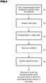
- Fig.4 illustrates a method of fabricating a capacitive structure according to certain embodiments of the present invention, for example the structure illustrated in Fig.3 .
- the illustrated method includes a process (S1) of forming an electrically conductive interconnection layer, e.g. layer 158, on a substrate and forming an anodization-resistant layer, e.g. layer 159, on the interconnection layer.
- S1 any suitable deposition techniques may be used, for example: chemical vapour deposition, physical vapour deposition, and so on.
- additional layers may be provided between the substrate and the interconnection layer 158, and between the interconnection layer 158 and the anodization-resistant layer 159.
- additional layers to improve adhesion may be interposed between the substrate and the interconnection layer 158, and between the interconnection layer 158 and the anodization-resistant layer 159.
- a laminated structure formed of a stack of thin Ti and TiN layers may be provided as an adhesion-improvement layer.
- a metal layer is then formed (S2) on the anodization-resistant layer by any suitable method, for example: chemical vapour deposition, physical vapour deposition, and so on.
- the thickness of this metal layer is typically in the range 1 ⁇ m-20 ⁇ m.
- An anodization process (S3) is performed to anodize a region of the metal layer to form a region of porous anodic oxide, e.g. 152a, traversed by a plurality of elongated pores extending between the anodization-resistant layer and a surface of the anodic oxide remote from the substrate.
- a mask may be used to define the region of the metal which is to be subjected to anodization.
- S3 some undesired oxide is formed at the bottoms of the pores.
- the undesired oxide is removed to open the pore bottoms (S4).
- the oxide may be removed by any suitable technique appropriate to the material used as the anodization-resistant layer; for example, by wet etching during which pH is controlled, and so on.
- the layers of the capacitive stack e.g. layers 153, 154 and 155
- the layers of the capacitive stack are deposited conformally over the pores in the region of porous anodic oxide by any suitable method, for example: atomic layer deposition, chemical vapour deposition and so on.
- the thicknesses of the layers may be set to ensure that relation (1) above is respected.
- the operating conditions of the anodization process may be set and controlled, as is known, with a view to obtaining an array of elongated pores which, on average, have a target pore diameter and a target inter-pore spacing. Not all of the pores in the final structure have the target pore diameter and target inter-pore spacing, but the operating conditions can be set and controlled so that, statistically, a greater or lesser percentage of the pores respect the target values.
- the method of Fig.4 is performed to produce a capacitive structure in which, in at least 1% of the pores of the porous anodic oxide region, the first portion of the capacitive stack of layers, which contributes to the capacitance of the capacitive structure, is formed in portions of the pores that are between a restricted-diameter position in the pore and the surface of the anodic oxide remote from the substrate.
- the anodization process (S3) may be controlled so that, towards the end, when material in the anodization-resistant layer begins to migrate and form undesired oxide plugs, the lateral size of the oxide plugs is controlled, thereby affecting the diameter of the restricted-diameter part of the pore.
- onset of the stage where material in the anodization-resistant layer begins to migrate and form undesired oxide plugs can be detected, for example, by measuring the electric current being drawn during the anodization process.
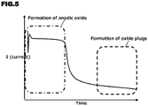
- Fig.5 illustrates a typical pattern of variation of current during the process of anodizing an aluminium layer to form anodic aluminium oxide (AAO).
- AAO anodic aluminium oxide
- the anodization conditions are deliberately changed part way through the anodization step, so as to slow down the rate of anodization during the time period when the anodization-resistant layer 158 is generating undesired oxide plugs.
- By slowing down the anodization process at this stage it becomes easier to exercise fine control of the size, in the lateral direction (i.e. the left-to-right direction in Fig.3 ), of the undesired oxide plugs.
- An example of a technique that can be used to slow down the anodization process at this stage is reduction of the operating temperature.
- Another technique that may be used to help to ensure that relationship (1) above is respected is to determine the size of the diameter of the pores at the reduced-diameter location and then set the thicknesses of the first conductive layer and first insulating layer of the capacitive stack based on the diameter of the reduced-diameter location.
- the pore diameter at the restricted-diameter position could be measured in each individual capacitive structure, after its fabrication, but time can be saved by performing experiments ahead of time to determine what diameter value D is produced by particular sets of fabrication conditions (e.g. for a particular profile of the anodization process).
- the thicknesses of the conductive and insulating layers of the capacitive stack may be set as a function of the desired capacitance value of the final structure.
Landscapes
- Engineering & Computer Science (AREA)
- Power Engineering (AREA)
- Microelectronics & Electronic Packaging (AREA)
- Manufacturing & Machinery (AREA)
- Chemical & Material Sciences (AREA)
- Ceramic Engineering (AREA)
- Inorganic Chemistry (AREA)
- Materials Engineering (AREA)
- Semiconductor Integrated Circuits (AREA)
- Fixed Capacitors And Capacitor Manufacturing Machines (AREA)
Abstract
Description
- The present invention relates to the field of electrical/electronic devices and to methods of their fabrication. More particularly, the invention relates to devices that incorporate three-dimensional capacitive structures, and to methods of manufacturing such devices.
- In recent years, as part of the trend to increase the degree of integration of electronic components, a need has arisen for integrated capacitors having increased capacitance density. One of the solutions that has been adopted to achieve a higher capacitance density is to amplify the surface area of electrodes that are used to provide capacitance. For example, a silicon capacitor which has been proposed by Murata Integrated Passive Solutions was fabricated in a process that employed semiconductor technologies to form three-dimensional structures (relief, texture), such as holes, trenches or columns, in silicon and then layers of metal/dielectric were formed conformally over the 3D structure to provide large-area electrodes.
- Another approach that has been proposed for providing a high-density capacitor consists in creating a porous region of anodic metal oxide (e.g. anodic aluminium oxide, AAO) and then depositing a single or repeated Metal-Insulator-Metal (MIM) stack structure conformally over the porous region, such that the MIM layers follow the contours of the pores and have a resultant large surface area. According to this approach, typically, a metal layer (for example, an aluminium layer) is formed on a silicon substrate and then an anodization process is performed on a selected region of the metal layer to create there a high density of uniform, self-assembled trenches, or "pores". This porous region of anodic oxide acts as a template upon which conductive layers and dielectric layers are then deposited. Strictly speaking the pores are defined in an anodic metal oxide layer that forms during the anodization process.
Fig.1A illustrates a template of the above-described kind formed by anodization. - Use of porous anodic oxide is an effective technique to enhance the surface area of the electrodes, but there can be a problem in achieving a sufficiently-low Equivalent Series Resistance (ESR) of the fabricated capacitive structure. To overcome this difficulty, a proposal has been made (
WO2015/063420 ) to remove the anodic oxide layer at the bottoms of the pores so that the interior of each pore can be brought into communication with a stack of electrically conductive layers provided at the substrate side. In this way, the lower layer of the MIM stack in each pore is connected, on the substrate side, to the lower layer of the MIM stack in an adjacent pore, lowering the ESR of the overall structure. -
Fig.1B is a simplified diagram illustrating acapacitive structure 50 of the general kind described inWO2015/063420 . Aregion 52a of porous AAO is formed in analuminium layer 52 provided on asilicon substrate 51. More specifically, thealuminium layer 52 is formed on a stack of layers comprising: a lower electrically-conductive layer 58, and anupper layer 59 which is resistant to anodization/anodic etching. The pores in theanodic oxide region 52a are open at the substrate side. Accordingly, afirst metal layer 53 that is formed conformally over theporous region 52a comes into contact with the underlying stack oflayers resistant layer 59 has sufficient electrical conductivity to enable a good electrical connection to be made, at the bottoms of the pores, between the electrically-conductive layer 58 and thefirst metal layer 53. Adielectric layer 54 and second electricallyconductive layer 55 form, with the firstconductive layer 53, a MIM stack which functions as a capacitive element. - Typically, a first terminal of the capacitive element is formed on the
side 56 remote from the substrate by making a connection to the secondconductive layer 55. The second terminal of the capacitive element may be formed on either side of the structure (i.e. on theside 56 or on the substrate side) by making a connection to the electricallyconductive layer 58. - It has been found that the yield of the manufacturing process which makes capacitive structures of the type illustrated in
Fig.1B depends on the thickness of thelayers Table 1 Thickness of electrically- conductive layer 58Thickness of anodization- resistant layer 59Manufacturing yield Thin Thin High Thin Thick Medium Thick Thin Medium Thick Thick Low - It can be seen from Table 1 that the best yield is obtained when both of the
layers layer 59 compared to layer 58). However, in order to obtain a good reduction in ESR it is preferable for thelayers - Experiments have been performed to investigate what phenomena may affect the yield of the manufacturing process and it is believed that the condition of the surface of the anodization-resistant layer may have a significant impact on the performance of the capacitive stack.
- From examination of the micro-structure of the architecture, using scanning electron microscopy, it has been found that there can be cracks in the anodization-
resistant layer 59. A crack labelled C is indicated schematically inFig.1B, and Fig.1C is an image, obtained by scanning electron microscopy, showing a crack in an anodization-resistant layer made of tungsten (W). These cracks can adversely affect the portions of the MIM stack that are formed at the bottoms of the pores and thereby cause an undesired leakage current to flow. Studies have shown that, in a typical case, cracks can affect the pores over 0.6% of the surface area of the useable porous region. - The present invention has been made in the light of the above-described problems.
- The present invention provides a capacitive structure comprising:
- a substrate providing an electrically-conductive
- interconnection layer;
- an anodization-resistant layer formed over the interconnection layer and making electrical contact with the interconnection layer;
- a region of porous anodic oxide formed on the anodization-resistant layer, the region of porous anodic oxide being traversed by a plurality of elongated pores extending between the anodization-resistant layer and a surface of the anodic oxide remote from the substrate; and
- a capacitive stack of layers comprising first and second conductive layers separated by a first insulator layer, said stack being formed conformally over the pores in said region of porous anodic oxide and having a first portion which contributes to the capacitance of the capacitive structure and a second portion which makes a negligible contribution to the capacitance of the capacitive structure,
- wherein:
- the pores have a position, along their length, where the pore diameter is restricted, and
- in a first, non-zero percentage of the pores of said region of porous anodic oxide, the first portion of the capacitive stack of layers, which contributes to the capacitance of the capacitive structure, extends into the pores no further than the position where the pore diameter is restricted.
- In capacitive structures according to embodiments of the present invention, in the first percentage of the pores of the anodic oxide region, the functional portion of the capacitive stack which contributes to the capacitance of the finished structure is not in direct contact with the portion of the anodization-resistant layer where cracks may arise. Accordingly, the negative effects of such cracks are reduced. More particularly, undesired leakage current is reduced and the electrical characteristics of the finished structure are improved, thereby the yield of the process used for manufacturing the structures can be improved. In view of the yield improvement, it becomes feasible to make use of relatively thicker layers for the anodization-resistant layer and the electrically-conductive interconnection layer, which facilitates the achievement of a low value of ESR at the same time as a high capacitance density. So, for example, it becomes feasible to use an anodization-resistant layer which is 600 nm thick and an interconnection layer which is 3 µm thick. These are just examples of the dimensions of relatively-thick layers that may be used; other thicknesses may be employed.
- Furthermore, as shall be explained below, by locating the functional portion of the capacitive stack above the position where the pore diameter is reduced, there is a reduction in the irregularity of the shape, near the bottoms of the pores, of the functional portion of the MIM stack which contributes to the capacitance of the finished structure. Accordingly, the target properties of the capacitive structure can be obtained more reliably, achieving a capacitive component having improved reliability and increased lifetime.
- Moreover, typically the aspect ratio of the pores is high and, at the bottoms of the pores, it is difficult to deposit the layers of the capacitive stack to the desired thickness. This can adversely affect the ESR and breakdown voltage of the overall capacitive structure. However, by locating the functional portion of the capacitive stack above the position where the pore diameter is reduced, non-uniformity in the thickness of the layers of the capacitive stack in the vicinity of the bottoms of the pores has reduced effect (potentially, negligible effect) on the performance of the overall capacitive structure.
- In certain embodiments of the invention, in at least 1% of the pores of the porous anodic oxide region the first portion of the capacitive stack of layers, which contributes to the capacitance of the capacitive structure, is located in portions of the pores that are between the restricted-diameter position and the surface of the anodic oxide remote from the substrate.
- In certain embodiments of the invention the first conductive layer of the stack is formed conformally over the pores in the porous region, the first insulator layer is formed on the first conductive layer, the second conductive layer is formed on the first insulator layer, and the second conductive layer extends into the pores no further than the position of reduced pore diameter. Because the second conductive layer does not extend beyond the reduced-diameter position in the pores, the functional portion of the capacitive structure (including both of the first and second conductive layers as well as the interposed insulating layer) is located between the reduced-diameter position in the pores and the surface of the anodic oxide region that is remote from the substrate.
- In certain embodiments of the invention, the following relationship is set:

- By ensuring that the above relationship is respected, the second conductive layer can be prevented from extending into the pores beyond the position of reduced pore diameter.
- In certain embodiments of the invention the position of reduced-diameter of the pores is located at a distance of 10-300 nm from the bottom of the pores.
- In certain embodiments of the invention the anodization-resistant layer is made of tungsten. However, the anodization-resistant layer may be made of other materials including, but not limited to, Ti, Ta, Hf and Nd. In certain embodiments of the invention the average thickness of the anodization-resistant layer is in the range 10 nm - 1 µm. In certain embodiments of the invention the anodic oxide is anodic aluminium oxide. However, the porous material may be made of other substances including, but not limited to porous anodized Ti, Si, Ta or Zr.
- The present invention still further provides a method of fabricating a capacitive structure, comprising:
- forming a substrate providing an electrically-conductive interconnection layer;
- forming over the interconnection layer an anodization-resistant layer making electrical contact with the interconnection layer;
- forming a metal layer on the anodization-resistant layer;
- anodizing a region of the metal layer to form a region of porous anodic oxide traversed by a plurality of elongated pores extending between the anodization-resistant layer and a surface of the anodic oxide remote from the substrate;
- removing oxide formed, at the bottoms of the pores, from the anodization-resistant layer during the anodizing step; and
- forming conformally over the pores in said region of porous anodic oxide a capacitive stack of layers comprising first and second conductive layers separated by a first insulator layer, said stack having a first portion which contributes to the capacitance of the capacitive structure and a second portion which makes a negligible contribution to the capacitance of the capacitive structure;
- wherein:
- the pores have a position, along their length, where the pore diameter is restricted, and
- at least one of the anodizing step, oxide-removing step and capacitive-stack forming step is controlled so that, in a first percentage of the pores of the porous anodic oxide region, the first portion of the capacitive stack of layers, which contributes to the capacitance of the capacitive structure, is formed in portions of the pores that are between the restricted-diameter position and the surface of the anodic oxide remote from the substrate.
- The above-recited method provides comparable advantages to those mentioned above in relation to the capacitive structure. Moreover, this method has improved yield compared to prior fabrication methods.
- Further features and advantages of the present invention will become apparent from the following description of certain embodiments thereof, given by way of illustration only, not limitation, with reference to the accompanying drawings in which:
-
Figure 1 illustrates known structures incorporating porous anodic oxide, in which:-
Fig.1A schematically illustrates a porous anodic aluminium oxide template formed on a substrate, -
Fig.1B illustrates a capacitive structure formed in a region of porous anodic oxide and having reduced equivalent series resistance, and -
Fig.1C shows a scanning electron micrograph illustrating a crack in an anodization-resistant layer present in structures such as that ofFig.1B ;
-
-
Figure 2 illustrates how pores in structures such as that ofFig.1B can have positions of reduced diameter, in which:-
Fig.2A is a cross-sectional view schematically illustrating reduced-diameter positions in the pores, and -
Fig.2B represents a scanning electron micrograph illustrating, highly magnified, the bottoms of the pores;
-
-
Figure 3 illustrate, schematically, a capacitive structure according to an embodiment of the invention; -
Figure 4 is a flow diagram illustrating the main stages in a method, according to an embodiment of the present invention, for fabricating a capacitive structure such as that ofFig.3 ; and -
Figure 5 illustrates how electric current varies during an anodization process. - The inventors have studied the potential origin of the cracks that can occur in the anodization-resistant layer. Their studies suggest that such cracks may arise because there are weak points in the anodization-
resistant layer 59 in the vicinity of the bottoms of the pores. The current understanding of the origin of such weak points is explained below. - During fabrication of a capacitive structure such as the
structure 50 illustrated inFig.1B , an anodization process is performed to create the pores of the porousanodic oxide region 52a, and the anodization process is continued until the bottoms of the pores are opened, to a sufficient degree, onto theupper layer 59. During that part of the anodization process which opens the pore bottoms, there is a certain degree of migration of atoms of the material (e.g. tungsten, W) forming the anodization-resistant layer 59 at regions which underlie the pores, and undesired small regions of oxide (e.g. tungsten oxide) are formed. Each of these small regions of undesired oxide is shaped roughly like a biconvex lens. Before deposition of the MIM stack in the pores this undesired oxide is removed, typically by an etching process. It is believed that this migration of atoms in the material forming the anodization-resistant layer 59 results in weak points in theanodization layer 59, and a propensity to cracking. - In view of this technical analysis, techniques have been devised for mitigating the negative effects of such cracks in the anodization-resistant layer. Embodiments of the invention exploit the fact that the pores in the anodic oxide may have a position of reduced diameter, this position being towards the bottoms of the pores.
- It has been realized that, as illustrated schematically in
Fig.2A , the pores formed by the manufacturing method described above with reference toFig.1B do not have a uniform cross-sectional area along the entirety of their length. Instead, they have an unusual and characteristic shape as can be seen inFig.2B which is an enlarged view of the bottoms of a set of pores, produced by scanning electron micrography. - More particularly, it has been found that there is a reduced-diameter neck portion, N, near the bottom of each pore at a position close to the anodization-
resistant layer 59. The position of this reduced-diameter of the pores is not directly above the surface of the anodization-resistant layer 59, typically it arises between 10 nm to 300 nm from that surface (e.g. in the case of using a tungsten layer as the anodization-resistant layer). Also, the periphery of the pore has a fan-like shape in the region under the location having minimum pore diameter. Considered another way, there is a roughly annular spur S extending into the pore at a position not far from the anodization-resistant layer. It is understood that this characteristic shape arises due to the formation and removal of the undesired oxide during that part of the anodization process which opens the bottoms of the pores. - In embodiments of the invention, the capacitive stack is formed in the pores of the anodic oxide region so that, in at least 1% of the pores, a functional portion F of the capacitive stack, which determines the capacitance of the overall structure, is located above the reduced-diameter position in the pores ("above" meaning further from the substrate than the position of reduced pore diameter). Thus, the performance of the capacitive stack is less affected by the surface condition of the anodization-resistant layer, e.g. cracks formed therein.
- Various approaches may be used to form the functional portion of the capacitive stack above the reduced-diameter position in the pores. Below there is a description of certain techniques which control a relationship between the thickness of certain layers in the capacitive stack and the diameter of the pore at the position having reduced-diameter, so as to ensure that the functional portion of the capacitive stack is located above the reduced-diameter position in the pores. More particularly, according to these techniques the first conductive layer and first insulating layer of the capacitive stack have thicknesses, relative to the diameter of the reduced-diameter location in the pores, which mean that these layers clog the bottom of the pores and the second conductive layer does not pass through the "throat" of the reduced-diameter location. In other words:

- A capacitive stack according to an embodiment of the invention will now be described with reference to
Fig.3 , and an example embodiment of a method to fabricate this structure will be described with reference toFig.4 . - As can be seen from the partial, enlarged view shown in
Fig.3 , acapacitive structure 150 according to the present embodiment includes aregion 152a of porous anodic oxide formed on a stack of layers comprising: a lower electrically-conductive layer 158, and anupper layer 159 which is resistant to anodization/anodic etching. The stack oflayers separate layer 158. The pores in theanodic oxide region 152a are open at the substrate side and have a position P where the diameter of the pore is reduced. The reduced-diameter position in the pore has a diameter designated D. - A first electrically-
conductive layer 153 is formed conformally over theporous region 152a and comes into contact with the underlying stack oflayers resistant layer 159 has sufficient electrical conductivity to enable a good electrical connection to be made, at the bottoms of the pores, between the electrically-conductive layer 158 and the firstconductive layer 153. In the embodiment illustrated inFig.3 , the firstconductive layer 153 is coated on the walls of the pore and follows the generally-cylindrical shape along the majority of the pore's length, as well as following the shape of the pore wall at the bottom of the pore. Thus, the firstconductive layer 153 passes through the reduced-diameter throat of the pore at position P and makes contact with the anodization-resistant layer 159.Fig.3 illustrates a single pore in a region of porous anodic oxide but it will be understood that, in practice, the firstconductive layer 153 will conformally coat the walls of a group of adjacent pores in the region of porous anodic oxide. - As shown in
Fig.3 , a first insulatinglayer 154 is provided on the firstconductive layer 153 and generally follows the shape of the underlying firstconductive layer 153. However, the thicknesses of the firstconductive layer 153 and the first insulatinglayer 154 are such that the reduced-diameter throat of the pore is closed off. More particularly, the first insulatinglayer 154 coating opposing surfaces of the pore makes contact with itself at a location just above the reduced-diameter position P in the pore. So, the inner surface of the first insulatinglayer 154 defines a generally cylindrical bore whose diameter is substantially constant along its length. A second electrically-conductive layer 155 is provided on the inner surface of the first insulatinglayer 154. The secondconductive layer 155 does not pass through the reduced-diameter throat of the pore; instead it conformally follows the shape of the inner surface of the first insulatinglayer 154 and, thus, it has a regular shape. - The second electrically
conductive layer 155 forms a capacitive stack with the firstconductive layer 153 and the intervening first insulatinglayer 154. A capacitive stack having layers of these kinds is often referred to as a MIM stack (from "metal-insulator-metal") even though the conductive layers may be formed of materials which are not pure metals. - The second
conductive layer 155 is not present below the position P where the pore has reduced diameter. It is only the portion F of the stacked layers, where all three of the first conductive layer, first insulating layer and second conductive layer are present, that is operational as a capacitor. However, the lower section of the first conductive layer, which coats the pore walls at, and underneath, the position P having reduced pore-diameter, makes electrical contact between the functional portion F of the capacitive stack and the underlying interconnection layers 158, 159. - The capacitive stack may be formed of extra layers additional to the
layers - The first conductive layer may be made of TiN. Typically, the thickness of the first
conductive layer 153 is in the range 1 nm-30 nm and may, for example, be approximately 10 nm. The material of the firstconductive layer 153 is not limited to TiN and may, for example, be made of TiAIN, TaN, TaAIN, Ru, RuO2, W, Ni, Co, Al, Ag, Au, Cu and Si. - The first insulating layer may be made of SiO2. Typically, the thickness of the first insulating
layer 154 is in the range 1 nm-30 nm and may, for example, be approximately 5 nm. The material of the first insulatinglayer 154 is not limited to SiO2 and may, for example, be made of Al2O3, HfO2, ZrO2, TiO2, La2O3, Y2O3, SrTiO3 and their silicates and aluminates, and laminated structures. - The second conductive layer may be made of TiN. Typically, the thickness of the second
conductive layer 155 is in the range 1 nm-30 nm and may, for example, be approximately 10 nm. The material of the secondconductive layer 155 is not limited to TiN and may, for example, be made of TiAIN, TaN, TaAIN, Ru, RuO2, W, Ni, Co, Al, Ag, Au, Cu and Si. - The anodization-
resistant layer 159 may be made of W. Typically, the thickness of the anodization-resistant layer 159 is in the range 10 nm-1um. The material of the anodization-resistant layer 159 is not limited to W and may, for example, be made of Ti, Ta, Hf and Nd. - The
interconnection layer 158, if provided, may be made of AlCu. Typically, the thickness of theinterconnection layer 158 is in the range 100 nm-5 µm, with thicknesses of 140 nm or above being preferred in view of ESR considerations. The material of theinterconnection layer 158 is not limited to AlCu and may, for example, be made of Al, AISi and AlSiCu. - The substrate (not shown) may be made of p++ doped silicon. The material of the substrate is not limited to p++ doped silicon and may, for example, be made of n-doped or non-doped Si, poly-Si and glass substrate.
- Capacitive structures according to the invention may be stacked on top of one another, in comparable manner to the capacitive structures described in
WO2015/063420 . Accordingly, lateral isolation bands may be provided in the structure, as described inWO2015/063420 . -
Fig.4 illustrates a method of fabricating a capacitive structure according to certain embodiments of the present invention, for example the structure illustrated inFig.3 . The illustrated method includes a process (S1) of forming an electrically conductive interconnection layer,e.g. layer 158, on a substrate and forming an anodization-resistant layer,e.g. layer 159, on the interconnection layer. In this process S1 any suitable deposition techniques may be used, for example: chemical vapour deposition, physical vapour deposition, and so on. If desired, additional layers (not shown) may be provided between the substrate and theinterconnection layer 158, and between theinterconnection layer 158 and the anodization-resistant layer 159. Thus, for example, additional layers to improve adhesion may be interposed between the substrate and theinterconnection layer 158, and between theinterconnection layer 158 and the anodization-resistant layer 159. For instance, a laminated structure formed of a stack of thin Ti and TiN layers may be provided as an adhesion-improvement layer. - A metal layer is then formed (S2) on the anodization-resistant layer by any suitable method, for example: chemical vapour deposition, physical vapour deposition, and so on. The thickness of this metal layer is typically in the range 1 µm-20 µm.
- An anodization process (S3) is performed to anodize a region of the metal layer to form a region of porous anodic oxide, e.g. 152a, traversed by a plurality of elongated pores extending between the anodization-resistant layer and a surface of the anodic oxide remote from the substrate. A mask may be used to define the region of the metal which is to be subjected to anodization.
- In general, during the anodization process S3 some undesired oxide is formed at the bottoms of the pores. The undesired oxide is removed to open the pore bottoms (S4). The oxide may be removed by any suitable technique appropriate to the material used as the anodization-resistant layer; for example, by wet etching during which pH is controlled, and so on.
- Next, the layers of the capacitive stack, e.g. layers 153, 154 and 155, are deposited conformally over the pores in the region of porous anodic oxide by any suitable method, for example: atomic layer deposition, chemical vapour deposition and so on. As noted above, the thicknesses of the layers may be set to ensure that relation (1) above is respected.
- The operating conditions of the anodization process may be set and controlled, as is known, with a view to obtaining an array of elongated pores which, on average, have a target pore diameter and a target inter-pore spacing. Not all of the pores in the final structure have the target pore diameter and target inter-pore spacing, but the operating conditions can be set and controlled so that, statistically, a greater or lesser percentage of the pores respect the target values. In embodiments of the invention, the method of
Fig.4 is performed to produce a capacitive structure in which, in at least 1% of the pores of the porous anodic oxide region, the first portion of the capacitive stack of layers, which contributes to the capacitance of the capacitive structure, is formed in portions of the pores that are between a restricted-diameter position in the pore and the surface of the anodic oxide remote from the substrate. - Different techniques can be used to ensure that relationship (1) above is respected. Thus, for example, the anodization process (S3) may be controlled so that, towards the end, when material in the anodization-resistant layer begins to migrate and form undesired oxide plugs, the lateral size of the oxide plugs is controlled, thereby affecting the diameter of the restricted-diameter part of the pore.
- Anodization processes suitable to produce a regular array of nanoscale pores in anodic oxide are known and so shall not be described in detail here. However, when applying such processes during the fabrication of capacitive structures according to embodiments of the invention, it can be advantageous to adapt the know processes.
- So, for example, the onset of the stage where material in the anodization-resistant layer begins to migrate and form undesired oxide plugs can be detected, for example, by measuring the electric current being drawn during the anodization process.
Fig.5 illustrates a typical pattern of variation of current during the process of anodizing an aluminium layer to form anodic aluminium oxide (AAO). The point at which it is appropriate to stop anodization in order to achieve a particular width of the oxide plugs can be determined by measuring the time elapsed after a particular current value is attained. - In certain embodiments of the invention, the anodization conditions are deliberately changed part way through the anodization step, so as to slow down the rate of anodization during the time period when the anodization-
resistant layer 158 is generating undesired oxide plugs. By slowing down the anodization process at this stage, it becomes easier to exercise fine control of the size, in the lateral direction (i.e. the left-to-right direction inFig.3 ), of the undesired oxide plugs. An example of a technique that can be used to slow down the anodization process at this stage is reduction of the operating temperature. - Another technique that may be used to help to ensure that relationship (1) above is respected is to determine the size of the diameter of the pores at the reduced-diameter location and then set the thicknesses of the first conductive layer and first insulating layer of the capacitive stack based on the diameter of the reduced-diameter location. In principle, the pore diameter at the restricted-diameter position could be measured in each individual capacitive structure, after its fabrication, but time can be saved by performing experiments ahead of time to determine what diameter value D is produced by particular sets of fabrication conditions (e.g. for a particular profile of the anodization process).
- In general, it may be preferable to set the thicknesses of the conductive and insulating layers of the capacitive stack as a function of the desired capacitance value of the final structure. Thus, it may be preferable to first design the specification of the capacitive stack and then to control the anodization process so as to produce pores whose reduced-diameter position has a diameter D which ensures that relation (1) above is respected.
- Although the present invention has been described above with reference to certain specific embodiments, it will be understood that the invention is not limited by the particularities of the specific embodiments. Numerous variations, modifications and developments may be made in the specified embodiments within the scope of the appended claims.
Claims (16)
- A capacitive structure comprising:a substrate providing an electrically-conductiveinterconnection layer;an anodization-resistant layer formed over the interconnection layer and making electrical contact with the interconnection layer;a region of porous anodic oxide formed on the anodization-resistant layer, the region of porous anodic oxide being traversed by a plurality of elongated pores extending between the anodization-resistant layer and a surface of the anodic oxide remote from the substrate; anda capacitive stack of layers comprising first and second conductive layers separated by a first insulator layer, said stack being formed conformally over the pores in said region of porous anodic oxide and having a first portion which contributes to the capacitance of the capacitive structure and a second portion which makes a negligible contribution to the capacitance of the capacitive structure,wherein:the pores have a position, along their length, where the pore diameter is restricted, andin a first, non-zero percentage of the pores of said region of porous anodic oxide, the first portion of the capacitive stack of layers, which contributes to the capacitance of the capacitive structure, is located in portions of the pores that are between the restricted-diameter position and the surface of the anodic oxide remote from the substrate.
- A capacitive structure according to claim 1, wherein the first conductive layer of the stack is formed conformally over the pores in the porous region, the first insulator layer is formed on the first conductive layer, and the second conductive layer is formed on the first insulator layer, and wherein the second conductive layer extends into the pores no further than said position of reduced-diameter.
- A capacitive structure according to claim 2, wherein:

- A capacitive structure according to any one of claims 1 to 3, wherein said position of reduced-diameter of the pores is located at a distance of 10-300 nm from the bottom of the pores.
- A capacitive structure according to any one of claims 1 to 4, wherein in at least 1% of the pores of the porous anodic oxide region the first portion of the capacitive stack of layers, which contributes to the capacitance of the capacitive structure, is located in portions of the pores that are between the restricted-diameter position and the surface of the anodic oxide remote from the substrate.
- A capacitive structure according to any one of claims 1 to 5, wherein the anodization-resistant layer is made of tungsten.
- A capacitive structure according to any one of claims 1 to 6, wherein the average thickness of the anodization-resistant layer is in the range 10 nm - 1 µm.
- A capacitive structure according to any one of claims 1 to 7, wherein the anodic oxide is anodic aluminium oxide.
- A method of fabricating a capacitive structure comprising:forming a substrate providing an electrically-conductive interconnection layer;forming over the interconnection layer an anodization-resistant layer making electrical contact with the interconnection layer;forming a metal layer on the anodization-resistant layer;anodizing a region of the metal layer to form a region of porous anodic oxide traversed by a plurality of elongated pores extending between the anodization-resistant layer and a surface of the anodic oxide remote from the substrate;removing oxide formed, at the bottoms of the pores, from the anodization-resistant layer during the anodizing step; andforming conformally over the pores in said region of porous anodic oxide a capacitive stack of layers comprising first and second conductive layers separated by a first insulator layer, said stack having a first portion which contributes to the capacitance of the capacitive structure and a second portion which makes a negligible contribution to the capacitance of the capacitive structure;wherein:the pores have a position, along their length, where the pore diameter is restricted, andat least one of the anodizing step, oxide-removing step and capacitive-stack forming step is controlled so that, in at least 1% of the pores of the porous anodic oxide region, the first portion of the capacitive stack of layers, which contributes to the capacitance of the capacitive structure, is formed in portions of the pores that are between the restricted-diameter position and the surface of the anodic oxide remote from the substrate.
- A capacitive-structure fabrication method according to claim 9, wherein the first conductive layer of the stack is formed conformally over the pores in the porous region, the first insulator layer is formed on the first conductive layer, and the second conductive layer is formed on the first insulator layer, and wherein the second conductive layer extends into the pores no further than said position of reduced-diameter.
- A capacitive-structure fabrication method according to claim 10, wherein:

- A capacitive-structure fabrication method according to any one of claims 9 to 11, wherein said position of reduced-diameter of the pores is located at a distance of 10-300 nm from the bottom of the pores.
- A capacitive-structure fabrication method according to any one of claims 9 to 12, wherein in at least 1% of the pores of the porous anodic oxide region the first portion of the capacitive stack of layers, which contributes to the capacitance of the capacitive structure, is located in portions of the pores that are between the restricted-diameter position and the surface of the anodic oxide remote from the substrate.
- A capacitive-structure fabrication method according to any one of claims 9 to 13, wherein the anodization-resistant layer is made of tungsten.
- A capacitive-structure fabrication method according to any one of claims 9 to 14, wherein the average thickness of the anodization-resistant layer is in the range 10 nm - 1 µm.
- A capacitive-structure fabrication method according to any one of claims 9 to 15, wherein the anodic oxide is anodic aluminium oxide.
Priority Applications (6)
| Application Number | Priority Date | Filing Date | Title |
|---|---|---|---|
| EP19305457.4A EP3723148A1 (en) | 2019-04-08 | 2019-04-08 | Three-dimensional capacitive structures and their manufacturing methods |
| CN202080027445.2A CN113661581B (en) | 2019-04-08 | 2020-04-06 | Three-dimensional capacitive structure and its manufacturing method |
| PCT/EP2020/059820 WO2020207988A1 (en) | 2019-04-08 | 2020-04-06 | Three-dimensional capacitive structures and their manufacturing methods |
| KR1020217036035A KR102721589B1 (en) | 2019-04-08 | 2020-04-06 | 3D capacitive structures and methods for their manufacture |
| TW109111628A TWI877158B (en) | 2019-04-08 | 2020-04-07 | Three-dimensional capacitive structures and their manufacturing methods |
| US17/496,185 US11978766B2 (en) | 2019-04-08 | 2021-10-07 | Three-dimensional capacitive structures and their manufacturing methods |
Applications Claiming Priority (1)
| Application Number | Priority Date | Filing Date | Title |
|---|---|---|---|
| EP19305457.4A EP3723148A1 (en) | 2019-04-08 | 2019-04-08 | Three-dimensional capacitive structures and their manufacturing methods |
Publications (1)
| Publication Number | Publication Date |
|---|---|
| EP3723148A1 true EP3723148A1 (en) | 2020-10-14 |
Family
ID=66286282
Family Applications (1)
| Application Number | Title | Priority Date | Filing Date |
|---|---|---|---|
| EP19305457.4A Pending EP3723148A1 (en) | 2019-04-08 | 2019-04-08 | Three-dimensional capacitive structures and their manufacturing methods |
Country Status (6)
| Country | Link |
|---|---|
| US (1) | US11978766B2 (en) |
| EP (1) | EP3723148A1 (en) |
| KR (1) | KR102721589B1 (en) |
| CN (1) | CN113661581B (en) |
| TW (1) | TWI877158B (en) |
| WO (1) | WO2020207988A1 (en) |
Cited By (2)
| Publication number | Priority date | Publication date | Assignee | Title |
|---|---|---|---|---|
| EP4060697A1 (en) * | 2021-03-18 | 2022-09-21 | Commissariat à l'énergie atomique et aux énergies alternatives | High-density capacitive device and method for manufacturing such a device |
| US11948719B2 (en) | 2019-09-30 | 2024-04-02 | Murata Manufacturing Co., Ltd. | Nanomagnetic inductor cores, inductors and devices incorporating such cores, and associated manufacturing methods |
Families Citing this family (3)
| Publication number | Priority date | Publication date | Assignee | Title |
|---|---|---|---|---|
| CN116133362B (en) * | 2021-08-04 | 2026-03-27 | 长鑫存储技术有限公司 | Semiconductor structure and its formation method |
| KR20240086344A (en) * | 2022-12-09 | 2024-06-18 | (주)포인트엔지니어링 | Capacitor Component and Integrated Circuit Chip Package Having the Same |
| EP4730381A1 (en) * | 2024-10-21 | 2026-04-22 | Murata Manufacturing Co., Ltd. | An integrated structure with an anodization barrier layer formed on a protective liner, and corresponding method |
Citations (2)
| Publication number | Priority date | Publication date | Assignee | Title |
|---|---|---|---|---|
| WO2015063420A1 (en) | 2013-10-29 | 2015-05-07 | Ipdia | Structure with an improved capacitor |
| US20190088419A1 (en) * | 2017-09-21 | 2019-03-21 | Samsung Electro-Mechanics Co., Ltd. | Capacitor component |
Family Cites Families (6)
| Publication number | Priority date | Publication date | Assignee | Title |
|---|---|---|---|---|
| CN1127136C (en) * | 1998-05-29 | 2003-11-05 | 世界先进积体电路股份有限公司 | Method of fabricating random access memory cell array |
| US20070235342A1 (en) * | 2004-10-01 | 2007-10-11 | Canon Kabushiki Kaisha | Method for manufacturing nanostructure |
| WO2012054042A1 (en) * | 2010-10-21 | 2012-04-26 | Hewlett-Packard Development Company, L.P. | Method of forming a nano-structure |
| TWI540739B (en) * | 2013-09-12 | 2016-07-01 | 璨圓光電股份有限公司 | Capacitor structure and stacked capacitor structure |
| EP3420571A4 (en) * | 2016-02-25 | 2020-03-25 | 3D Glass Solutions, Inc. | PHOTOACTIVE SUBSTRATES FOR MANUFACTURING A 3D CAPACITOR AND A CAPACITOR ARRAY |
| CN105789266A (en) * | 2016-05-30 | 2016-07-20 | 京东方科技集团股份有限公司 | OLED array substrate, making method thereof and display device |
-
2019
- 2019-04-08 EP EP19305457.4A patent/EP3723148A1/en active Pending
-
2020
- 2020-04-06 WO PCT/EP2020/059820 patent/WO2020207988A1/en not_active Ceased
- 2020-04-06 KR KR1020217036035A patent/KR102721589B1/en active Active
- 2020-04-06 CN CN202080027445.2A patent/CN113661581B/en active Active
- 2020-04-07 TW TW109111628A patent/TWI877158B/en active
-
2021
- 2021-10-07 US US17/496,185 patent/US11978766B2/en active Active
Patent Citations (3)
| Publication number | Priority date | Publication date | Assignee | Title |
|---|---|---|---|---|
| WO2015063420A1 (en) | 2013-10-29 | 2015-05-07 | Ipdia | Structure with an improved capacitor |
| US20160268144A1 (en) * | 2013-10-29 | 2016-09-15 | Ipdia | Structure with an improved capacitor |
| US20190088419A1 (en) * | 2017-09-21 | 2019-03-21 | Samsung Electro-Mechanics Co., Ltd. | Capacitor component |
Non-Patent Citations (2)
| Title |
|---|
| DUSAN LOSIC ET AL: "Porous Alumina with Shaped Pore Geometries and Complex Pore Architectures Fabricated by Cyclic Anodization", SMALL, vol. 5, no. 12, 19 June 2009 (2009-06-19), pages 1392 - 1397, XP055003997, ISSN: 1613-6810, DOI: 10.1002/smll.200801645 * |
| WOO LEE ET AL: "Highly ordered porous alumina with tailor-made pore structures fabricated by pulse anodization", NANOTECHNOLOGY, IOP, BRISTOL, GB, vol. 21, no. 48, 10 November 2010 (2010-11-10), pages 485304 1 - 8, XP020201563, ISSN: 0957-4484, DOI: 10.1088/0957-4484/21/48/485304 * |
Cited By (5)
| Publication number | Priority date | Publication date | Assignee | Title |
|---|---|---|---|---|
| US11948719B2 (en) | 2019-09-30 | 2024-04-02 | Murata Manufacturing Co., Ltd. | Nanomagnetic inductor cores, inductors and devices incorporating such cores, and associated manufacturing methods |
| US12191064B2 (en) | 2019-09-30 | 2025-01-07 | Murata Manufacturing Co., Ltd. | Nanomagnetic inductor cores, inductors and devices incorporating such cores, and associated manufacturing methods |
| EP4060697A1 (en) * | 2021-03-18 | 2022-09-21 | Commissariat à l'énergie atomique et aux énergies alternatives | High-density capacitive device and method for manufacturing such a device |
| FR3120982A1 (en) * | 2021-03-18 | 2022-09-23 | Commissariat A L'energie Atomique Et Aux Energies Alternatives | HIGH DENSITY CAPACITIVE DEVICE AND METHOD FOR FABRICATING SUCH A DEVICE |
| US12476051B2 (en) | 2021-03-18 | 2025-11-18 | Commissariat à l'énergie atomique et aux énergies alternatives | High-density capacitive device and method for manufacturing such a device |
Also Published As
| Publication number | Publication date |
|---|---|
| TW202044585A (en) | 2020-12-01 |
| TWI877158B (en) | 2025-03-21 |
| US20220093726A1 (en) | 2022-03-24 |
| KR102721589B1 (en) | 2024-10-25 |
| US11978766B2 (en) | 2024-05-07 |
| WO2020207988A1 (en) | 2020-10-15 |
| CN113661581B (en) | 2026-04-17 |
| CN113661581A (en) | 2021-11-16 |
| KR20210144889A (en) | 2021-11-30 |
Similar Documents
| Publication | Publication Date | Title |
|---|---|---|
| US11978766B2 (en) | Three-dimensional capacitive structures and their manufacturing methods | |
| US11316006B2 (en) | Porous region structure and method of manufacture thereof | |
| US12054838B2 (en) | Semiconductor device having porous region embedded structure and method of manufacture thereof | |
| US11705484B2 (en) | Nanowire structure enhanced for stack deposition | |
| US12431291B2 (en) | Capacitor structure with via embedded in porous medium | |
| US20220208480A1 (en) | Low defect high capacitance thin solid electrolyte capacitor and method of fabrication thereof | |
| US12406811B2 (en) | Device having an anodic porous region surrounded by a trench having an electrical isolation barrier | |
| EP4435153A1 (en) | An integrated device having plugged up pores in an island or a protuberance, and corresponding method | |
| CN118251121A (en) | Integrated device including an anodic porous oxide region and method of making the same | |
| US20230386751A2 (en) | A method for manufacturing an electrical device with an anodic porous oxide region delimited by planarizing a stack of materials | |
| CN112119512B (en) | Porous region structure and method of manufacturing the same | |
| EP3901997A1 (en) | Electrical device for characterizing a deposition step such as atomic layer deposition (ald), and corresponding methods of fabricating and characterizing | |
| EP4376064A1 (en) | A method for obtaining an integrated device comprising using an etching mask to define dicing lines | |
| US20220301784A1 (en) | High-density capacitive device and method for manufacturing such a device | |
| US20070096253A1 (en) | Integrated capacitor with a high breakdown voltage |
Legal Events
| Date | Code | Title | Description |
|---|---|---|---|
| PUAI | Public reference made under article 153(3) epc to a published international application that has entered the european phase |
Free format text: ORIGINAL CODE: 0009012 |
|
| STAA | Information on the status of an ep patent application or granted ep patent |
Free format text: STATUS: THE APPLICATION HAS BEEN PUBLISHED |
|
| AK | Designated contracting states |
Kind code of ref document: A1 Designated state(s): AL AT BE BG CH CY CZ DE DK EE ES FI FR GB GR HR HU IE IS IT LI LT LU LV MC MK MT NL NO PL PT RO RS SE SI SK SM TR |
|
| AX | Request for extension of the european patent |
Extension state: BA ME |
|
| STAA | Information on the status of an ep patent application or granted ep patent |
Free format text: STATUS: REQUEST FOR EXAMINATION WAS MADE |
|
| 17P | Request for examination filed |
Effective date: 20210413 |
|
| RBV | Designated contracting states (corrected) |
Designated state(s): AL AT BE BG CH CY CZ DE DK EE ES FI FR GB GR HR HU IE IS IT LI LT LU LV MC MK MT NL NO PL PT RO RS SE SI SK SM TR |
|
| RAP3 | Party data changed (applicant data changed or rights of an application transferred) |
Owner name: COMMISSARIAT A L'ENERGIE ATOMIQUE ET AUX ENERGIESALTERNATIVES Owner name: MURATA MANUFACTURING CO., LTD. |
|
| STAA | Information on the status of an ep patent application or granted ep patent |
Free format text: STATUS: EXAMINATION IS IN PROGRESS |
|
| 17Q | First examination report despatched |
Effective date: 20260323 |