EP3722919A1 - Memory socket protecting cover and memory socket assembly - Google Patents
Memory socket protecting cover and memory socket assembly Download PDFInfo
- Publication number
- EP3722919A1 EP3722919A1 EP19191713.7A EP19191713A EP3722919A1 EP 3722919 A1 EP3722919 A1 EP 3722919A1 EP 19191713 A EP19191713 A EP 19191713A EP 3722919 A1 EP3722919 A1 EP 3722919A1
- Authority
- EP
- European Patent Office
- Prior art keywords
- fool
- memory
- memory socket
- wear
- proof
- Prior art date
- Legal status (The legal status is an assumption and is not a legal conclusion. Google has not performed a legal analysis and makes no representation as to the accuracy of the status listed.)
- Granted
Links
Images



Classifications
-
- G—PHYSICS
- G06—COMPUTING OR CALCULATING; COUNTING
- G06F—ELECTRIC DIGITAL DATA PROCESSING
- G06F1/00—Details not covered by groups G06F3/00 - G06F13/00 and G06F21/00
- G06F1/16—Constructional details or arrangements
- G06F1/18—Packaging or power distribution
- G06F1/183—Internal mounting support structures, e.g. for supporting printed circuit boards
- G06F1/185—Mounting of expansion boards
-
- H—ELECTRICITY
- H01—ELECTRIC ELEMENTS
- H01R—ELECTRICALLY-CONDUCTIVE CONNECTIONS; STRUCTURAL ASSOCIATIONS OF A PLURALITY OF MUTUALLY-INSULATED ELECTRICAL CONNECTING ELEMENTS; COUPLING DEVICES; CURRENT COLLECTORS
- H01R12/00—Structural associations of a plurality of mutually-insulated electrical connecting elements, specially adapted for printed circuits, e.g. printed circuit boards [PCB], flat or ribbon cables, or like generally planar structures, e.g. terminal strips, terminal blocks; Coupling devices specially adapted for printed circuits, flat or ribbon cables, or like generally planar structures; Terminals specially adapted for contact with, or insertion into, printed circuits, flat or ribbon cables, or like generally planar structures
- H01R12/70—Coupling devices
- H01R12/7005—Guiding, mounting, polarizing or locking means; Extractors
-
- H—ELECTRICITY
- H01—ELECTRIC ELEMENTS
- H01R—ELECTRICALLY-CONDUCTIVE CONNECTIONS; STRUCTURAL ASSOCIATIONS OF A PLURALITY OF MUTUALLY-INSULATED ELECTRICAL CONNECTING ELEMENTS; COUPLING DEVICES; CURRENT COLLECTORS
- H01R13/00—Details of coupling devices of the kinds covered by groups H01R12/70 or H01R24/00 - H01R33/00
- H01R13/46—Bases; Cases
- H01R13/502—Bases; Cases composed of different pieces
-
- G—PHYSICS
- G06—COMPUTING OR CALCULATING; COUNTING
- G06F—ELECTRIC DIGITAL DATA PROCESSING
- G06F1/00—Details not covered by groups G06F3/00 - G06F13/00 and G06F21/00
- G06F1/16—Constructional details or arrangements
- G06F1/1613—Constructional details or arrangements for portable computers
- G06F1/1633—Constructional details or arrangements of portable computers not specific to the type of enclosures covered by groups G06F1/1615 - G06F1/1626
- G06F1/1656—Details related to functional adaptations of the enclosure, e.g. to provide protection against EMI, shock, water, or to host detachable peripherals like a mouse or removable expansions units like PCMCIA cards, or to provide access to internal components for maintenance or to removable storage supports like CDs or DVDs, or to mechanically mount accessories
- G06F1/1658—Details related to functional adaptations of the enclosure, e.g. to provide protection against EMI, shock, water, or to host detachable peripherals like a mouse or removable expansions units like PCMCIA cards, or to provide access to internal components for maintenance or to removable storage supports like CDs or DVDs, or to mechanically mount accessories related to the mounting of internal components, e.g. disc drive or any other functional module
-
- G—PHYSICS
- G06—COMPUTING OR CALCULATING; COUNTING
- G06F—ELECTRIC DIGITAL DATA PROCESSING
- G06F1/00—Details not covered by groups G06F3/00 - G06F13/00 and G06F21/00
- G06F1/16—Constructional details or arrangements
- G06F1/18—Packaging or power distribution
- G06F1/183—Internal mounting support structures, e.g. for supporting printed circuit boards
-
- H—ELECTRICITY
- H01—ELECTRIC ELEMENTS
- H01R—ELECTRICALLY-CONDUCTIVE CONNECTIONS; STRUCTURAL ASSOCIATIONS OF A PLURALITY OF MUTUALLY-INSULATED ELECTRICAL CONNECTING ELEMENTS; COUPLING DEVICES; CURRENT COLLECTORS
- H01R12/00—Structural associations of a plurality of mutually-insulated electrical connecting elements, specially adapted for printed circuits, e.g. printed circuit boards [PCB], flat or ribbon cables, or like generally planar structures, e.g. terminal strips, terminal blocks; Coupling devices specially adapted for printed circuits, flat or ribbon cables, or like generally planar structures; Terminals specially adapted for contact with, or insertion into, printed circuits, flat or ribbon cables, or like generally planar structures
- H01R12/70—Coupling devices
- H01R12/71—Coupling devices for rigid printing circuits or like structures
- H01R12/72—Coupling devices for rigid printing circuits or like structures coupling with the edge of the rigid printed circuits or like structures
- H01R12/721—Coupling devices for rigid printing circuits or like structures coupling with the edge of the rigid printed circuits or like structures cooperating directly with the edge of the rigid printed circuits
-
- H—ELECTRICITY
- H01—ELECTRIC ELEMENTS
- H01R—ELECTRICALLY-CONDUCTIVE CONNECTIONS; STRUCTURAL ASSOCIATIONS OF A PLURALITY OF MUTUALLY-INSULATED ELECTRICAL CONNECTING ELEMENTS; COUPLING DEVICES; CURRENT COLLECTORS
- H01R12/00—Structural associations of a plurality of mutually-insulated electrical connecting elements, specially adapted for printed circuits, e.g. printed circuit boards [PCB], flat or ribbon cables, or like generally planar structures, e.g. terminal strips, terminal blocks; Coupling devices specially adapted for printed circuits, flat or ribbon cables, or like generally planar structures; Terminals specially adapted for contact with, or insertion into, printed circuits, flat or ribbon cables, or like generally planar structures
- H01R12/70—Coupling devices
- H01R12/71—Coupling devices for rigid printing circuits or like structures
- H01R12/72—Coupling devices for rigid printing circuits or like structures coupling with the edge of the rigid printed circuits or like structures
- H01R12/73—Coupling devices for rigid printing circuits or like structures coupling with the edge of the rigid printed circuits or like structures connecting to other rigid printed circuits or like structures
- H01R12/735—Printed circuits including an angle between each other
- H01R12/737—Printed circuits being substantially perpendicular to each other
-
- H—ELECTRICITY
- H01—ELECTRIC ELEMENTS
- H01R—ELECTRICALLY-CONDUCTIVE CONNECTIONS; STRUCTURAL ASSOCIATIONS OF A PLURALITY OF MUTUALLY-INSULATED ELECTRICAL CONNECTING ELEMENTS; COUPLING DEVICES; CURRENT COLLECTORS
- H01R13/00—Details of coupling devices of the kinds covered by groups H01R12/70 or H01R24/00 - H01R33/00
- H01R13/64—Means for preventing incorrect coupling
-
- H—ELECTRICITY
- H01—ELECTRIC ELEMENTS
- H01R—ELECTRICALLY-CONDUCTIVE CONNECTIONS; STRUCTURAL ASSOCIATIONS OF A PLURALITY OF MUTUALLY-INSULATED ELECTRICAL CONNECTING ELEMENTS; COUPLING DEVICES; CURRENT COLLECTORS
- H01R13/00—Details of coupling devices of the kinds covered by groups H01R12/70 or H01R24/00 - H01R33/00
- H01R13/46—Bases; Cases
- H01R13/516—Means for holding or embracing insulating body, e.g. casing, hoods
Definitions
- the invention relates to a socket protecting cover and a socket assembly and more particularly, to a memory socket protecting cover and a memory socket assembly.
- a memory slot includes a fool-proof member disposed therein for preventing a user from inversely inserting a memory module.
- the fool-proof member is commonly a product manufactured by means of plastic injection.
- the invention provides a memory socket protecting cover capable of reducing a probability that a fool-proof member of a memory socket is worn, such that goldfingers on a memory module is capable of being accurately inserted into a memory slot.
- the invention provides a memory socket assembly having the aforementioned memory socket protecting cover.
- a memory socket protecting cover of the invention is adapted to be assembled to a memory socket which is adapted for a memory module to insert is provided.
- the memory module includes a fool-proof concave
- the memory socket includes a fool-proof member corresponding to the fool-proof concave.
- the memory socket protecting cover includes two lateral walls and a wear-resistant member.
- the two lateral walls are adapted to be disposed at two sides of the memory socket.
- the wear-resistant member is connected to the two lateral walls and adapted to be disposed on the fool-proof member.
- a width of the wear-resistant member is greater than or equal to a width of the fool-proof member and is smaller than a width of the fool-proof concave.
- a memory socket assembly of the invention is adapted for a memory module to insert.
- the memory module includes a fool-proof concave
- the memory socket assembly includes a memory socket and a memory socket protecting cover.
- the memory socket includes a fool-proof member corresponding to the fool-proof concave.
- the memory socket protecting cover is assembled to the memory socket.
- the memory socket protecting cover includes two lateral walls and a wear-resistant member. The two lateral walls are disposed at two sides of the memory socket.
- the wear-resistant member is connected to the two lateral walls and disposed on the fool-proof member.
- a width of the wear-resistant member is greater than or equal to a width of the fool-proof member and is smaller than a width of the fool-proof concave.
- the wear-resistant member includes a first portion, a second portion and a third portion which are sequentially connected together, the second portion is connected to the two lateral walls and adapted to be located on a top surface of the fool-proof member, and the first portion and the third portion are adapted to be respectively located at two sides of the fool-proof member.
- the first portion, the second portion and the third portion present a U-shaped column.
- the first portion, the second portion and the third portion present a J-shaped column.
- the wear-resistant member presents an I-shaped column, the wear-resistant member is adapted to be located on the top surface of the fool-proof member, and a thickness of the wear-resistant member is greater than a thickness of each of the lateral walls.
- the memory socket has a memory slot and two positioning grooves located at the two sides of the fool-proof member, an extension direction of the two positioning grooves is perpendicular to an extension direction of the memory slot, the two positioning grooves communicate with the memory slot, and the first portion and the third portion are inserted into the two positioning grooves to be positioned.
- the wear-resistant member of the memory socket protecting cover of the invention is adapted to be disposed on the fool-proof member of the memory socket, and the width of the wear-resistant member is greater than or equal to the width of the fool-proof member, such that when the memory module is inserted in or pulled from the memory socket, the wall of the memory module besides the fool-proof concave contacts the wear-resistant member, thereby reducing the probability that the fool-proof member of the memory socket is worn, as well as mitigating the issues between the goldfingers on the memory module and the pads inside the memory slot, such as poor contact, offset misalignment or short circuit.
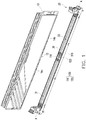
- FIG. 1 is a schematic diagram illustrating a memory socket assembly which a memory module is not yet inserted into according to an embodiment of the invention.
- FIG. 2 is a schematic exploded diagram of the memory socket assembly depicted in FIG. 1 .
- a memory socket assembly 20 of the present embodiment is adapted for a memory module 10 to insert.
- the memory module 10 is, for example, a DDR4 memory module 10, but the type of the memory module 10 is not limited thereto.
- the memory module 10 includes a fool-proof concave 12.
- the fool-proof concave 12 separates goldfinger terminals 14a and 14b of the memory module 10 into, for example, two sections having different lengths.
- the memory socket assembly 20 includes a memory socket 30 and a memory socket protecting cover 100.
- the memory socket 30 has memory slots 31 and 33 for the memory module 10 to insert, and the memory socket 30 includes a fool-proof member 32 corresponding to the fool-proof concave 12.
- the fool-proof member 30 separates the memory slots 31 and 33 into, for example, two sections having different lengths, so as to prevent a user from inversely inserting the goldfinger terminals 14a and 14b of the memory module 10 into the memory slots 31 and 33.
- the memory socket protecting cover 100 is assembled to the memory socket 30 for improving structure strength of the memory socket 30.
- the memory socket protecting cover 100 includes two lateral walls 110 and a wear-resistant member 120.
- the two lateral walls 110 are disposed at two long side surfaces of the memory socket 30.
- the memory socket protecting cover 100 further includes two short walls 130 connected to the two lateral walls 110.
- the two short walls 130 correspond to two short side surfaces of the memory socket 30.
- the memory socket protecting cover 100 has a frame-shaped appearance, thereby providing preferable structure strength.
- the type of the memory socket protecting cover 100 is not limited thereto.
- a material of the memory socket protecting cover 100 is, for example, metal.
- the memory socket protecting cover 100 is made of, for example, iron, copper or stainless steel.
- the material of the memory socket protecting cover 100 is not limited thereto, and any material capable of providing preferable structure strength is applicable thereto.
- the memory socket protecting cover 100 is made of metal, it is capable of providing preferable heat dissipation, and the heat generated during the operation process of the memory module 10 may also be guided to the memory socket protecting cover 100 to enhance the heat dissipation effect.
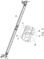
- FIG. 3 is a schematic cross-sectional diagram of the memory socket assembly depicted in FIG. 1 .
- FIG. 4A is a schematic cross-sectional diagram of the memory module inserted in to the memory socket assembly depicted in FIG. 1 .
- FIG. 4B is a schematic partially enlarged diagram of FIG. 4A .
- the wear-resistant member 120 is connected to the two lateral walls 110 and disposed on the fool-proof member 32.
- the wear-resistant member 120 includes a first portion 122, a second portion 124 and a third portion 126 which are sequentially connected together.
- the second portion 124 is connected to the two lateral walls 110 and located on a top surface of the fool-proof member 32, and the first portion 122 and the third portion 126 are respectively located at two sides of the fool-proof member 32.
- lengths of the first portion 122 and the third portion 126 are approximately equal to each other, and the first portion 122, the second portion 124 and the third portion 126 present a U-shaped column, but the type of the wear-resistant member 120 is not limited thereto.
- the memory socket 30 has two positioning grooves 34 located at the two sides of the fool-proof member 32.
- An extension direction of the two positioning grooves 34 is perpendicular to an extension direction of the memory slots 31 and 33.
- the two positioning grooves 34 communicate with the memory slots 31 and 33.
- the first portion 122 and the third portion 126 of the wear-resistant member 120 are inserted into the two positioning grooves 34 of the memory socket 30 to be positioned.
- the first portion 122 and the third portion 126 may also be prevented from being opened outwards by the two positioning grooves 34, thereby preventing the wear-resistant member 120 from being deformed or being separated from the fool-proof member 32.
- a width W1 of the wear-resistant member 120 is greater than or equal to a width W2 of the fool-proof member 32.
- the wear-resistant member 120 covered on the fool-proof member 32 may serve as a wear-resistant structure for protecting the fool-proof member 32.
- the wear-resistant member 120 since the width W1 of the wear-resistant member 120 is smaller than the width of the fool-proof concave 12, the wear-resistant member 120 does not block the memory module 10 from being inserted into the memory socket assembly 20. In this way, when the memory module 10 is inserted in or pulled from the memory socket 30, a wall of the memory module 10 besides the fool-proof concave 12 contacts the wear-resistant member 120, thereby preventing the fool-proof member 32 from being worn.
- the memory socket protecting cover 100 may be manufactured by punching or bending a metal plate or by other manufacturing processes. That is to say, a thickness of the wear-resistant member 120 is the same as a thickness of each of the lateral walls 110, but the form of the wear-resistant member 120 is not limited thereto.
- FIG. 5 is a schematic diagram of the memory socket assembly depicted in FIG. 1 in another view angle.
- the memory socket protecting cover 100 further includes at least one fixing pin 140, at least one engagement portion 150 and at least one protrusive structure 112.
- the numbers of the at least one fixing pin 140, the at least one engagement portion 150 and the at least one protrusive structure 112 may be plural respectively.
- These fixing pins 140 extend downward from the two lateral walls 110, so as to be inserted to a mainboard (not shown) and stably fixed to the mainboard.
- the engagement portions 150 are bent from the bottoms of the two lateral walls 110 toward a bottom portion 36 of the memory socket 30 to increase the strength that the memory socket protecting cover 100 is fixed to the memory socket 30.
- the protrusive structures 112 are located on the two lateral walls 110 and used to improve structure strength of the lateral walls 110.
- FIG. 6 through FIG. 8 are schematic partially cross-sectional diagrams illustrating various scenarios that the memory module is inserted into the memory socket assembly according to other embodiments of the invention.
- the main difference between a wear-resistant member 120a illustrated in FIG. 6 and the wear-resistant member 120 illustrated in FIG. 4B lies in the following.
- the lengths of the first portion 122 and the third portion 126 of the wear-resistant member 120 are approximately equal to each other, such that the first portion 122, the second portion 124 and the third portion 126 present the U-shaped column.
- lengths of a first portion 122 and a third portion 126a of the wear-resistant member 120a are not equal to each other.
- the length of the third portion 126a is smaller than the length of the first portion 122, such that the first portion 122, a second portion 124 and the third portion 126a present a J-shaped column.
- the third portion 126a of the wear-resistant member 120a may still be capable of protecting the fool-proof member 32, and when being inserted in or pulled from the memory socket 30, the memory module 10 may contact the wall of the memory module 10 besides the fool-proof concave 12 in replacement with the fool-proof member 32.
- a length of a third portion 126 of a wear-resistant member 120b illustrated in FIG. 7 is greater than a length of a first portion 122b. Even though the length of the first portion 122b illustrated in FIG. 7 is smaller, in the same way, a part of the left side of the fool-proof member 32 near the top surface is still covered by the first portion 126b. Thus, the first portion 126b of the wear-resistant member 120 may still be capable of protecting the fool-proof member 32, and when being inserted in or pulled from the memory socket 30, the memory module 10 may contact the wall of the memory module 10 besides the fool-proof concave 12 in replacement with the fool-proof member 32.
- a wear-resistant member 120c presents an I-shaped column.
- the wear-resistant member 120c is located on the top surface of the fool-proof member 32. Namely, in the present embodiment, the wear-resistant member 120c does not extend to the two sides of the fool-proof member 32.
- the wear-resistant member 120c is located on the top surface of the fool-proof member 32 and has the width W1 greater than or equal to the width W2 of the fool-proof member 32, when the memory module 10 is inserted in or pulled from the memory socket 30, the wall of the memory module 10 besides the fool-proof concave 12 still first contacts two sides of the wear-resistant member 120c, such that a probability that the fool-proof member 32 is worn by the wall of the memory module 10 besides the fool-proof concave 12 may be reduced.
- the wear-resistant member 120c has a specific thickness to provide the left and the right sides thereof to be contacted or worn by the wall of the memory module 10 besides the fool-proof concave 12.
- the thickness of the wear-resistant member 120c may be greater than a thickness of any other portion (e.g., the side wall 110) of the memory socket protecting cover 100.
- a manufacturer may fix the wear-resistant member 120c having the greater thickness to the two side walls 110 by means of soldering or adhering.
- the manufacturer may perform the manufacturing first by using a plate body having the same thickness through punching or bending the plate body and then increase the thickness of a portion where the wear-resistant member 120c is located by electroplating or sputtering the portion.
- the manufacturing and structure of the wear-resistant member 120c are not limited thereto.
- the wear-resistant member of the memory socket protecting cover of the invention is adapted to be disposed on the fool-proof member of the memory socket, and the width of the wear-resistant member is greater than or equal to the width of the fool-proof member, such that when the memory module is inserted in or pulled from the memory socket, the wall of the memory module besides the fool-proof concave contacts the wear-resistant member, thereby reducing a probability that a fool-proof member of a memory socket is worn, as well as reducing the issues between the goldfingers on the memory module and the pads inside the memory slot, such as poor contact, offset misalignment or short circuit.
Landscapes
- Engineering & Computer Science (AREA)
- Theoretical Computer Science (AREA)
- Computer Hardware Design (AREA)
- General Engineering & Computer Science (AREA)
- Human Computer Interaction (AREA)
- Physics & Mathematics (AREA)
- General Physics & Mathematics (AREA)
- Power Engineering (AREA)
- Details Of Connecting Devices For Male And Female Coupling (AREA)
- Connector Housings Or Holding Contact Members (AREA)
Abstract
Description
- The invention relates to a socket protecting cover and a socket assembly and more particularly, to a memory socket protecting cover and a memory socket assembly.
- At present, a memory slot includes a fool-proof member disposed therein for preventing a user from inversely inserting a memory module. The fool-proof member is commonly a product manufactured by means of plastic injection. When the memory module, after being plugged and unplugged for many times, is worn, that may further influence alignment accuracy between goldfingers on the memory module and pads inside a memory slot, which may cause issues between the goldfingers on the memory module and the pads inside the memory slot, such as poor contact, offset misalignment or short circuit.
- The invention provides a memory socket protecting cover capable of reducing a probability that a fool-proof member of a memory socket is worn, such that goldfingers on a memory module is capable of being accurately inserted into a memory slot.
- The invention provides a memory socket assembly having the aforementioned memory socket protecting cover.
- A memory socket protecting cover of the invention is adapted to be assembled to a memory socket which is adapted for a memory module to insert is provided. The memory module includes a fool-proof concave, and the memory socket includes a fool-proof member corresponding to the fool-proof concave. The memory socket protecting cover includes two lateral walls and a wear-resistant member. The two lateral walls are adapted to be disposed at two sides of the memory socket. The wear-resistant member is connected to the two lateral walls and adapted to be disposed on the fool-proof member. A width of the wear-resistant member is greater than or equal to a width of the fool-proof member and is smaller than a width of the fool-proof concave. When the memory module is inserted in or pulled from the memory socket, a wall of the memory module besides the fool-proof concave is adapted to contact the wear-resistant member.
- A memory socket assembly of the invention is adapted for a memory module to insert. The memory module includes a fool-proof concave, and the memory socket assembly includes a memory socket and a memory socket protecting cover. The memory socket includes a fool-proof member corresponding to the fool-proof concave. The memory socket protecting cover is assembled to the memory socket. The memory socket protecting cover includes two lateral walls and a wear-resistant member. The two lateral walls are disposed at two sides of the memory socket. The wear-resistant member is connected to the two lateral walls and disposed on the fool-proof member. A width of the wear-resistant member is greater than or equal to a width of the fool-proof member and is smaller than a width of the fool-proof concave. When the memory module is inserted in or pulled from the memory socket, a wall of the memory module besides the fool-proof concave is adapted to contact the wear-resistant member.
- In an embodiment of the invention, the wear-resistant member includes a first portion, a second portion and a third portion which are sequentially connected together, the second portion is connected to the two lateral walls and adapted to be located on a top surface of the fool-proof member, and the first portion and the third portion are adapted to be respectively located at two sides of the fool-proof member.
- In an embodiment of the invention, the first portion, the second portion and the third portion present a U-shaped column.
- In an embodiment of the invention, the first portion, the second portion and the third portion present a J-shaped column.
- In an embodiment of the invention, the wear-resistant member presents an I-shaped column, the wear-resistant member is adapted to be located on the top surface of the fool-proof member, and a thickness of the wear-resistant member is greater than a thickness of each of the lateral walls.
- In an embodiment of the invention, the memory socket has a memory slot and two positioning grooves located at the two sides of the fool-proof member, an extension direction of the two positioning grooves is perpendicular to an extension direction of the memory slot, the two positioning grooves communicate with the memory slot, and the first portion and the third portion are inserted into the two positioning grooves to be positioned.
- To sum up, the wear-resistant member of the memory socket protecting cover of the invention is adapted to be disposed on the fool-proof member of the memory socket, and the width of the wear-resistant member is greater than or equal to the width of the fool-proof member, such that when the memory module is inserted in or pulled from the memory socket, the wall of the memory module besides the fool-proof concave contacts the wear-resistant member, thereby reducing the probability that the fool-proof member of the memory socket is worn, as well as mitigating the issues between the goldfingers on the memory module and the pads inside the memory slot, such as poor contact, offset misalignment or short circuit.
- To make the above features and advantages of the invention more comprehensible, embodiments accompanied with drawings are described in detail below.
- The accompanying drawings are included to provide a further understanding of the invention, and are incorporated in and constitute a part of this specification. The drawings illustrate embodiments of the invention and, together with the description, serve to explain the principles of the invention.
-
FIG. 1 is a schematic diagram illustrating a memory socket assembly which a memory module is not yet inserted into according to an embodiment of the invention. -
FIG. 2 is a schematic exploded diagram of the memory socket assembly depicted inFIG. 1 . -
FIG. 3 is a schematic cross-sectional diagram of the memory socket assembly depicted inFIG. 1 . -
FIG. 4A is a schematic cross-sectional diagram of the memory module inserted in to the memory socket assembly depicted inFIG. 1 . -
FIG. 4B is a schematic partially enlarged diagram ofFIG. 4A . -
FIG. 5 is a schematic diagram of the memory socket assembly depicted inFIG. 1 in another view angle. -
FIG. 6 through FIG. 8 are schematic partially cross-sectional diagrams illustrating various scenarios that the memory module is inserted into the memory socket assembly according to other embodiments of the invention. -
FIG. 1 is a schematic diagram illustrating a memory socket assembly which a memory module is not yet inserted into according to an embodiment of the invention.FIG. 2 is a schematic exploded diagram of the memory socket assembly depicted inFIG. 1 . Referring toFIG. 1 andFIG. 2 , amemory socket assembly 20 of the present embodiment is adapted for amemory module 10 to insert. Thememory module 10 is, for example, aDDR4 memory module 10, but the type of thememory module 10 is not limited thereto. Thememory module 10 includes a fool-proof concave 12. The fool-proof concave 12 separatesgoldfinger terminals memory module 10 into, for example, two sections having different lengths. - With reference to
FIG. 2 , in the present embodiment, thememory socket assembly 20 includes amemory socket 30 and a memorysocket protecting cover 100. Thememory socket 30 hasmemory slots memory module 10 to insert, and thememory socket 30 includes a fool-proof member 32 corresponding to the fool-proof concave 12. The fool-proof member 30 separates thememory slots goldfinger terminals memory module 10 into thememory slots - The memory
socket protecting cover 100 is assembled to thememory socket 30 for improving structure strength of thememory socket 30. In the present embodiment, the memorysocket protecting cover 100 includes twolateral walls 110 and a wear-resistant member 120. The twolateral walls 110 are disposed at two long side surfaces of thememory socket 30. In the present embodiment, the memorysocket protecting cover 100 further includes twoshort walls 130 connected to the twolateral walls 110. The twoshort walls 130 correspond to two short side surfaces of thememory socket 30. In this way, the memorysocket protecting cover 100 has a frame-shaped appearance, thereby providing preferable structure strength. Certainly, the type of the memorysocket protecting cover 100 is not limited thereto. - In the present embodiment, a material of the memory
socket protecting cover 100 is, for example, metal. For instance, the memorysocket protecting cover 100 is made of, for example, iron, copper or stainless steel. Certainly, the material of the memorysocket protecting cover 100 is not limited thereto, and any material capable of providing preferable structure strength is applicable thereto. In the present embodiment, since the memorysocket protecting cover 100 is made of metal, it is capable of providing preferable heat dissipation, and the heat generated during the operation process of thememory module 10 may also be guided to the memorysocket protecting cover 100 to enhance the heat dissipation effect. -
FIG. 3 is a schematic cross-sectional diagram of the memory socket assembly depicted inFIG. 1 .FIG. 4A is a schematic cross-sectional diagram of the memory module inserted in to the memory socket assembly depicted inFIG. 1 .FIG. 4B is a schematic partially enlarged diagram ofFIG. 4A . - Referring to
FIG. 3 through FIG. 4B , in the present embodiment, the wear-resistant member 120 is connected to the twolateral walls 110 and disposed on the fool-proof member 32. The wear-resistant member 120 includes afirst portion 122, asecond portion 124 and athird portion 126 which are sequentially connected together. Thesecond portion 124 is connected to the twolateral walls 110 and located on a top surface of the fool-proof member 32, and thefirst portion 122 and thethird portion 126 are respectively located at two sides of the fool-proof member 32. In the present embodiment, lengths of thefirst portion 122 and thethird portion 126 are approximately equal to each other, and thefirst portion 122, thesecond portion 124 and thethird portion 126 present a U-shaped column, but the type of the wear-resistant member 120 is not limited thereto. - Moreover, referring to
FIG. 2 andFIG. 3 , in the present embodiment, thememory socket 30 has twopositioning grooves 34 located at the two sides of the fool-proof member 32. An extension direction of the twopositioning grooves 34 is perpendicular to an extension direction of thememory slots positioning grooves 34 communicate with thememory slots first portion 122 and thethird portion 126 of the wear-resistant member 120 are inserted into the twopositioning grooves 34 of thememory socket 30 to be positioned. When thememory module 10 is inserted in or pulled from thememory socket 30, thefirst portion 122 and thethird portion 126 may also be prevented from being opened outwards by the twopositioning grooves 34, thereby preventing the wear-resistant member 120 from being deformed or being separated from the fool-proof member 32. - As illustrated in
FIG. 4B , in the present embodiment, a width W1 of the wear-resistant member 120 is greater than or equal to a width W2 of the fool-proof member 32. Thus, the wear-resistant member 120 covered on the fool-proof member 32 may serve as a wear-resistant structure for protecting the fool-proof member 32. Moreover, since the width W1 of the wear-resistant member 120 is smaller than the width of the fool-proof concave 12, the wear-resistant member 120 does not block thememory module 10 from being inserted into thememory socket assembly 20. In this way, when thememory module 10 is inserted in or pulled from thememory socket 30, a wall of thememory module 10 besides the fool-proof concave 12 contacts the wear-resistant member 120, thereby preventing the fool-proof member 32 from being worn. - It is to be mentioned that in this embodiment, the memory
socket protecting cover 100 may be manufactured by punching or bending a metal plate or by other manufacturing processes. That is to say, a thickness of the wear-resistant member 120 is the same as a thickness of each of thelateral walls 110, but the form of the wear-resistant member 120 is not limited thereto. -
FIG. 5 is a schematic diagram of the memory socket assembly depicted inFIG. 1 in another view angle. Referring toFIG. 5 , in the present embodiment, the memorysocket protecting cover 100 further includes at least one fixingpin 140, at least oneengagement portion 150 and at least one protrusive structure 112. In the present embodiment, the numbers of the at least one fixingpin 140, the at least oneengagement portion 150 and the at least one protrusive structure 112 may be plural respectively. These fixingpins 140 extend downward from the twolateral walls 110, so as to be inserted to a mainboard (not shown) and stably fixed to the mainboard. Theengagement portions 150 are bent from the bottoms of the twolateral walls 110 toward abottom portion 36 of thememory socket 30 to increase the strength that the memorysocket protecting cover 100 is fixed to thememory socket 30. The protrusive structures 112 are located on the twolateral walls 110 and used to improve structure strength of thelateral walls 110. -
FIG. 6 through FIG. 8 are schematic partially cross-sectional diagrams illustrating various scenarios that the memory module is inserted into the memory socket assembly according to other embodiments of the invention. Referring toFIG. 6 first, the main difference between a wear-resistant member 120a illustrated inFIG. 6 and the wear-resistant member 120 illustrated inFIG. 4B lies in the following. InFIG. 4B , the lengths of thefirst portion 122 and thethird portion 126 of the wear-resistant member 120 are approximately equal to each other, such that thefirst portion 122, thesecond portion 124 and thethird portion 126 present the U-shaped column. InFIG. 6 , lengths of afirst portion 122 and athird portion 126a of the wear-resistant member 120a are not equal to each other. The length of thethird portion 126a is smaller than the length of thefirst portion 122, such that thefirst portion 122, asecond portion 124 and thethird portion 126a present a J-shaped column. - According to
FIG. 6 , even the lengths of thefirst portion 122 and thethird portion 126a of the wear-resistant member 120a are not equal to each other, inFIG. 6 , a part of the right side of the fool-proof member 32 near the top surface is still covered by thethird portion 126a. Thus, thethird portion 126a of the wear-resistant member 120a may still be capable of protecting the fool-proof member 32, and when being inserted in or pulled from thememory socket 30, thememory module 10 may contact the wall of thememory module 10 besides the fool-proof concave 12 in replacement with the fool-proof member 32. - Referring to
FIG. 7 , a length of athird portion 126 of a wear-resistant member 120b illustrated inFIG. 7 is greater than a length of afirst portion 122b. Even though the length of thefirst portion 122b illustrated inFIG. 7 is smaller, in the same way, a part of the left side of the fool-proof member 32 near the top surface is still covered by the first portion 126b. Thus, the first portion 126b of the wear-resistant member 120 may still be capable of protecting the fool-proof member 32, and when being inserted in or pulled from thememory socket 30, thememory module 10 may contact the wall of thememory module 10 besides the fool-proof concave 12 in replacement with the fool-proof member 32. - Referring to
FIG. 8 , in the present embodiment, a wear-resistant member 120c presents an I-shaped column. The wear-resistant member 120c is located on the top surface of the fool-proof member 32. Namely, in the present embodiment, the wear-resistant member 120c does not extend to the two sides of the fool-proof member 32. However, since the wear-resistant member 120c is located on the top surface of the fool-proof member 32 and has the width W1 greater than or equal to the width W2 of the fool-proof member 32, when thememory module 10 is inserted in or pulled from thememory socket 30, the wall of thememory module 10 besides the fool-proof concave 12 still first contacts two sides of the wear-resistant member 120c, such that a probability that the fool-proof member 32 is worn by the wall of thememory module 10 besides the fool-proof concave 12 may be reduced. - It is to be mentioned that in this embodiment, the wear-
resistant member 120c has a specific thickness to provide the left and the right sides thereof to be contacted or worn by the wall of thememory module 10 besides the fool-proof concave 12. Thus, the thickness of the wear-resistant member 120c may be greater than a thickness of any other portion (e.g., the side wall 110) of the memorysocket protecting cover 100. A manufacturer, for example, may fix the wear-resistant member 120c having the greater thickness to the twoside walls 110 by means of soldering or adhering. Alternatively, the manufacturer may perform the manufacturing first by using a plate body having the same thickness through punching or bending the plate body and then increase the thickness of a portion where the wear-resistant member 120c is located by electroplating or sputtering the portion. Certainly, the manufacturing and structure of the wear-resistant member 120c are not limited thereto. - Based on the above, the wear-resistant member of the memory socket protecting cover of the invention is adapted to be disposed on the fool-proof member of the memory socket, and the width of the wear-resistant member is greater than or equal to the width of the fool-proof member, such that when the memory module is inserted in or pulled from the memory socket, the wall of the memory module besides the fool-proof concave contacts the wear-resistant member, thereby reducing a probability that a fool-proof member of a memory socket is worn, as well as reducing the issues between the goldfingers on the memory module and the pads inside the memory slot, such as poor contact, offset misalignment or short circuit.
Claims (11)
- A memory socket protecting cover (100), adapted to be assembled to a memory socket (30), wherein the memory socket (30) is adapted for a memory module (10) to insert, the memory module (10) comprises a fool-proof concave (12), and the memory socket (30) comprises a fool-proof member (32) corresponding to the fool-proof concave (12), the memory socket protecting cover (100) comprising:two lateral walls (110), adapted to be disposed at two sides of the memory socket (30); anda wear-resistant member (120, 120a, 120b, 120c), connected to the two lateral walls (110) and adapted to be disposed on the fool-proof member (32), wherein a width of the wear-resistant member (120, 120a, 120b, 120c) is greater than or equal to a width of the fool-proof member (32) and is smaller than a width of the fool-proof concave (12),wherein when the memory module (10) is inserted in or pulled from the memory socket (30), a wall of the memory module (10) besides the fool-proof concave (12) is adapted to contact the wear-resistant member (120, 120a, 120b, 120c).
- The memory socket protecting cover (100) according to claim 1, wherein the wear-resistant member (120, 120a, 120b) comprises a first portion (122, 122b), a second portion (124) and a third portion (126, 126a) which are sequentially connected together, the second portion (124) is connected to the two lateral walls (110) and adapted to be located on a top surface of the fool-proof member (32), and the first portion (122, 122b) and the third portion (126, 126a) are adapted to be respectively located at two sides of the fool-proof member (32).
- The memory socket protecting cover (100) according to claim 2, wherein the first portion (122), the second portion (124) and the third portion (126) present a U-shaped column.
- The memory socket protecting cover (100) according to claim 2, wherein the first portion (122, 122b), the second portion (124) and the third portion (126a, 126) present a J-shaped column.
- The memory socket protecting cover (100) according to claim 1, wherein the wear-resistant member (120c) presents an I-shaped column, the wear-resistant member (120c) is adapted to be located on a top surface of the fool-proof member (32), and a thickness of the wear-resistant member (120c) is greater than a thickness of each of the lateral walls (110).
- A memory socket assembly (20), adapted for a memory module (10) to insert, wherein the memory module (10) comprises a fool-proof concave (12), the memory socket assembly (20) comprising:a memory socket (30), comprising a fool-proof member (32) corresponding to the fool-proof concave (12);a memory socket protecting cover (100), assembled to the memory socket (30), comprising:two lateral walls (110), disposed at two sides of the memory socket (30); anda wear-resistant member (120, 120a, 120b, 120c), connected to the two lateral walls (110) and disposed on the fool-proof member (32), wherein a width of the wear-resistant member (120, 120a, 120b, 120c) is greater than or equal to a width of the fool-proof member (32) and is smaller than a width of the fool-proof concave (12),wherein when the memory module (10) is inserted in or pulled from the memory socket (30), a wall of the memory module (10) besides the fool-proof concave (12) is adapted to contact the wear-resistant member (120, 120a, 120b, 120c).
- The memory socket assembly (20) according to claim 6, wherein the wear-resistant member (120, 120a, 120b) comprises a first portion (122, 122b), a second portion (124) and a third portion (126, 126a) which are sequentially connected together, the second portion (124) is connected to the two lateral walls (110) and located on a top surface of the fool-proof member (32), and the first portion (122, 122b) and the third portion (126, 126a) are respectively located at two sides of the fool-proof member (32).
- The memory socket assembly (20) according to claim 7, wherein the first portion (122), the second portion (124) and the third portion (126) present a U-shaped column.
- The memory socket assembly (20) according to claim 7, wherein the first portion (122, 122b), the second portion (124) and the third portion (126a, 126) present a J-shaped column.
- The memory socket assembly (20) according to any one of claims 7-9, wherein the memory socket (30) has a memory slot (31) and two positioning grooves (34) located at the two sides of the fool-proof member (32), an extension direction of the two positioning grooves (34) is perpendicular to an extension direction of the memory slot (31), the two positioning grooves (34) communicate with the memory slot (31), and the first portion (122, 122b) and the third portion (126, 126a) are inserted into the two positioning grooves (34) to be positioned.
- The memory socket assembly (20) according to claim 6, wherein the wear-resistant member (120c) presents an I-shaped column, the wear-resistant member (120c) is located on a top surface of the fool-proof member (32), and a thickness of the wear-resistant member (120c) is greater than a thickness of each of the lateral walls (110).
Applications Claiming Priority (1)
| Application Number | Priority Date | Filing Date | Title |
|---|---|---|---|
| TW108112424A TWI691968B (en) | 2019-04-10 | 2019-04-10 | Memory socket protecting cover and memory socket assembly |
Publications (2)
| Publication Number | Publication Date |
|---|---|
| EP3722919A1 true EP3722919A1 (en) | 2020-10-14 |
| EP3722919B1 EP3722919B1 (en) | 2024-05-08 |
Family
ID=67658808
Family Applications (1)
| Application Number | Title | Priority Date | Filing Date |
|---|---|---|---|
| EP19191713.7A Active EP3722919B1 (en) | 2019-04-10 | 2019-08-14 | Memory socket protecting cover and memory socket assembly |
Country Status (4)
| Country | Link |
|---|---|
| US (1) | US10707601B1 (en) |
| EP (1) | EP3722919B1 (en) |
| CN (1) | CN111817049A (en) |
| TW (1) | TWI691968B (en) |
Families Citing this family (4)
| Publication number | Priority date | Publication date | Assignee | Title |
|---|---|---|---|---|
| CN207705421U (en) * | 2017-12-19 | 2018-08-07 | 华为技术有限公司 | A kind of chip pocket and network system |
| CN109586065A (en) * | 2018-12-03 | 2019-04-05 | 番禺得意精密电子工业有限公司 | Electric connector |
| US11789877B2 (en) * | 2021-08-27 | 2023-10-17 | Dell Products, L.P. | Removable memory module coupling |
| KR102469398B1 (en) * | 2022-08-31 | 2022-11-21 | 황동원 | Memory module socket |
Citations (2)
| Publication number | Priority date | Publication date | Assignee | Title |
|---|---|---|---|---|
| CN205429312U (en) * | 2015-12-23 | 2016-08-03 | 番禺得意精密电子工业有限公司 | Connector |
| US20180090864A1 (en) * | 2016-09-27 | 2018-03-29 | Foxconn Interconnect Technology Limited | Card edge connector having key equipped with metallic protective cap secured to housing |
Family Cites Families (15)
| Publication number | Priority date | Publication date | Assignee | Title |
|---|---|---|---|---|
| JPH11233194A (en) * | 1997-07-23 | 1999-08-27 | Whitaker Corp:The | Circuit card holder and connector assembly using the same |
| US5943218A (en) * | 1998-06-01 | 1999-08-24 | Liu; Yen-Wen | Card type CPU-fixing structure |
| TW549700U (en) * | 2002-12-03 | 2003-08-21 | Egbon Electronics Ltd | Mistake proof structure improvement of memory card electrical connector |
| TWM256569U (en) * | 2003-12-09 | 2005-02-01 | Optimum Care Int Tech Inc | Memory module device |
| TWI236189B (en) * | 2004-10-18 | 2005-07-11 | P Two Ind Inc | Memory card connector |
| US7628655B1 (en) * | 2008-06-11 | 2009-12-08 | Lotes Co., Ltd. | Electrical connector and inserting method thereof |
| US7775811B2 (en) * | 2008-10-24 | 2010-08-17 | Giga-Byte Technology Co., Ltd. | Circuit board module and connector protecting cover thereof |
| CN102455750B (en) * | 2010-10-18 | 2015-04-08 | 无为县特种电缆产业技术研究院 | Bracket and memory set with same |
| CN202042635U (en) * | 2010-12-25 | 2011-11-16 | 富士康(昆山)电脑接插件有限公司 | card edge connector |
| TWM450884U (en) * | 2012-10-11 | 2013-04-11 | Carry Technology Co Ltd | Memory card adapter device |
| JP5990140B2 (en) * | 2013-08-09 | 2016-09-07 | 株式会社オートネットワーク技術研究所 | connector |
| TWI601340B (en) * | 2015-11-04 | 2017-10-01 | 技嘉科技股份有限公司 | Connector cover and connector assembly |
| TWI584534B (en) * | 2016-01-20 | 2017-05-21 | 技嘉科技股份有限公司 | Connector cover, connector and connector module |
| CN107204551B (en) * | 2016-03-17 | 2019-12-27 | 富士康(昆山)电脑接插件有限公司 | Card edge connector |
| CN206211099U (en) * | 2016-08-19 | 2017-05-31 | 富誉电子科技(淮安)有限公司 | Bayonet connector |
-
2019
- 2019-04-10 TW TW108112424A patent/TWI691968B/en active
- 2019-05-07 CN CN201910375995.2A patent/CN111817049A/en active Pending
- 2019-06-19 US US16/445,247 patent/US10707601B1/en active Active
- 2019-08-14 EP EP19191713.7A patent/EP3722919B1/en active Active
Patent Citations (2)
| Publication number | Priority date | Publication date | Assignee | Title |
|---|---|---|---|---|
| CN205429312U (en) * | 2015-12-23 | 2016-08-03 | 番禺得意精密电子工业有限公司 | Connector |
| US20180090864A1 (en) * | 2016-09-27 | 2018-03-29 | Foxconn Interconnect Technology Limited | Card edge connector having key equipped with metallic protective cap secured to housing |
Also Published As
| Publication number | Publication date |
|---|---|
| EP3722919B1 (en) | 2024-05-08 |
| TW202038222A (en) | 2020-10-16 |
| TWI691968B (en) | 2020-04-21 |
| CN111817049A (en) | 2020-10-23 |
| US10707601B1 (en) | 2020-07-07 |
Similar Documents
| Publication | Publication Date | Title |
|---|---|---|
| US10707601B1 (en) | Memory socket protecting cover and memory socket assembly | |
| JP6242936B2 (en) | Circuit board electrical connector | |
| JP4841756B2 (en) | Contact and electrical connector with this | |
| KR101241686B1 (en) | Board-to-board connector | |
| CN102144338B (en) | Board to board connector | |
| CN101582542B (en) | Connector | |
| EP3609024B1 (en) | Connector assembly | |
| KR101738337B1 (en) | Connector | |
| US6979235B2 (en) | Electrical plug-in connector with a housing and a high-current contact | |
| CN101316017A (en) | Connector | |
| US11605913B2 (en) | Connector and manufacturing method of connector | |
| US20090156048A1 (en) | Electrical Connector And Contact Insertion Guide | |
| US20170070014A1 (en) | Connector | |
| US7841879B2 (en) | Floating-type connector | |
| EP1467439B1 (en) | Electrical connector | |
| US20090156044A1 (en) | Electrical Connector and Contact Insertion Guide | |
| JP2025123472A (en) | electrical connectors | |
| WO2020004077A1 (en) | Electric connector having shielding plate, and manufacturing method for housing of electric connector | |
| CN1574497A (en) | Card connector capable of inhibiting insertion of a thinner card with a simple structure | |
| KR102853847B1 (en) | Connector with insert-molded terminal | |
| CN107104303B (en) | Electric connection terminal structure | |
| KR20200063479A (en) | Connector | |
| JP2024081331A (en) | Contact, connector, and connector assembly | |
| WO2023017766A1 (en) | Connector and electronic device | |
| EP3709446A1 (en) | Connector |
Legal Events
| Date | Code | Title | Description |
|---|---|---|---|
| PUAI | Public reference made under article 153(3) epc to a published international application that has entered the european phase |
Free format text: ORIGINAL CODE: 0009012 |
|
| STAA | Information on the status of an ep patent application or granted ep patent |
Free format text: STATUS: THE APPLICATION HAS BEEN PUBLISHED |
|
| AK | Designated contracting states |
Kind code of ref document: A1 Designated state(s): AL AT BE BG CH CY CZ DE DK EE ES FI FR GB GR HR HU IE IS IT LI LT LU LV MC MK MT NL NO PL PT RO RS SE SI SK SM TR |
|
| AX | Request for extension of the european patent |
Extension state: BA ME |
|
| STAA | Information on the status of an ep patent application or granted ep patent |
Free format text: STATUS: REQUEST FOR EXAMINATION WAS MADE |
|
| 17P | Request for examination filed |
Effective date: 20201102 |
|
| RBV | Designated contracting states (corrected) |
Designated state(s): AL AT BE BG CH CY CZ DE DK EE ES FI FR GB GR HR HU IE IS IT LI LT LU LV MC MK MT NL NO PL PT RO RS SE SI SK SM TR |
|
| STAA | Information on the status of an ep patent application or granted ep patent |
Free format text: STATUS: EXAMINATION IS IN PROGRESS |
|
| 17Q | First examination report despatched |
Effective date: 20211222 |
|
| GRAP | Despatch of communication of intention to grant a patent |
Free format text: ORIGINAL CODE: EPIDOSNIGR1 |
|
| STAA | Information on the status of an ep patent application or granted ep patent |
Free format text: STATUS: GRANT OF PATENT IS INTENDED |
|
| INTG | Intention to grant announced |
Effective date: 20240229 |
|
| RIN1 | Information on inventor provided before grant (corrected) |
Inventor name: CHUNG-WEI, CHIANG Inventor name: YUNG-SHUN, KAO Inventor name: CHIH-MING, LAI |
|
| GRAS | Grant fee paid |
Free format text: ORIGINAL CODE: EPIDOSNIGR3 |
|
| GRAA | (expected) grant |
Free format text: ORIGINAL CODE: 0009210 |
|
| STAA | Information on the status of an ep patent application or granted ep patent |
Free format text: STATUS: THE PATENT HAS BEEN GRANTED |
|
| AK | Designated contracting states |
Kind code of ref document: B1 Designated state(s): AL AT BE BG CH CY CZ DE DK EE ES FI FR GB GR HR HU IE IS IT LI LT LU LV MC MK MT NL NO PL PT RO RS SE SI SK SM TR |
|
| REG | Reference to a national code |
Ref country code: GB Ref legal event code: FG4D |
|
| REG | Reference to a national code |
Ref country code: CH Ref legal event code: EP |
|
| REG | Reference to a national code |
Ref country code: DE Ref legal event code: R096 Ref document number: 602019051829 Country of ref document: DE |
|
| REG | Reference to a national code |
Ref country code: IE Ref legal event code: FG4D |
|
| REG | Reference to a national code |
Ref country code: LT Ref legal event code: MG9D |
|
| REG | Reference to a national code |
Ref country code: NL Ref legal event code: MP Effective date: 20240508 |
|
| PG25 | Lapsed in a contracting state [announced via postgrant information from national office to epo] |
Ref country code: IS Free format text: LAPSE BECAUSE OF FAILURE TO SUBMIT A TRANSLATION OF THE DESCRIPTION OR TO PAY THE FEE WITHIN THE PRESCRIBED TIME-LIMIT Effective date: 20240908 |
|
| PG25 | Lapsed in a contracting state [announced via postgrant information from national office to epo] |
Ref country code: BG Free format text: LAPSE BECAUSE OF FAILURE TO SUBMIT A TRANSLATION OF THE DESCRIPTION OR TO PAY THE FEE WITHIN THE PRESCRIBED TIME-LIMIT Effective date: 20240508 |
|
| PG25 | Lapsed in a contracting state [announced via postgrant information from national office to epo] |
Ref country code: HR Free format text: LAPSE BECAUSE OF FAILURE TO SUBMIT A TRANSLATION OF THE DESCRIPTION OR TO PAY THE FEE WITHIN THE PRESCRIBED TIME-LIMIT Effective date: 20240508 Ref country code: FI Free format text: LAPSE BECAUSE OF FAILURE TO SUBMIT A TRANSLATION OF THE DESCRIPTION OR TO PAY THE FEE WITHIN THE PRESCRIBED TIME-LIMIT Effective date: 20240508 |
|
| PG25 | Lapsed in a contracting state [announced via postgrant information from national office to epo] |
Ref country code: GR Free format text: LAPSE BECAUSE OF FAILURE TO SUBMIT A TRANSLATION OF THE DESCRIPTION OR TO PAY THE FEE WITHIN THE PRESCRIBED TIME-LIMIT Effective date: 20240809 |
|
| PG25 | Lapsed in a contracting state [announced via postgrant information from national office to epo] |
Ref country code: PT Free format text: LAPSE BECAUSE OF FAILURE TO SUBMIT A TRANSLATION OF THE DESCRIPTION OR TO PAY THE FEE WITHIN THE PRESCRIBED TIME-LIMIT Effective date: 20240909 |
|
| REG | Reference to a national code |
Ref country code: AT Ref legal event code: MK05 Ref document number: 1685517 Country of ref document: AT Kind code of ref document: T Effective date: 20240508 |
|
| PG25 | Lapsed in a contracting state [announced via postgrant information from national office to epo] |
Ref country code: NL Free format text: LAPSE BECAUSE OF FAILURE TO SUBMIT A TRANSLATION OF THE DESCRIPTION OR TO PAY THE FEE WITHIN THE PRESCRIBED TIME-LIMIT Effective date: 20240508 |
|
| PG25 | Lapsed in a contracting state [announced via postgrant information from national office to epo] |
Ref country code: ES Free format text: LAPSE BECAUSE OF FAILURE TO SUBMIT A TRANSLATION OF THE DESCRIPTION OR TO PAY THE FEE WITHIN THE PRESCRIBED TIME-LIMIT Effective date: 20240508 |
|
| PG25 | Lapsed in a contracting state [announced via postgrant information from national office to epo] |
Ref country code: AT Free format text: LAPSE BECAUSE OF FAILURE TO SUBMIT A TRANSLATION OF THE DESCRIPTION OR TO PAY THE FEE WITHIN THE PRESCRIBED TIME-LIMIT Effective date: 20240508 |
|
| PG25 | Lapsed in a contracting state [announced via postgrant information from national office to epo] |
Ref country code: PL Free format text: LAPSE BECAUSE OF FAILURE TO SUBMIT A TRANSLATION OF THE DESCRIPTION OR TO PAY THE FEE WITHIN THE PRESCRIBED TIME-LIMIT Effective date: 20240508 |
|
| PG25 | Lapsed in a contracting state [announced via postgrant information from national office to epo] |
Ref country code: LV Free format text: LAPSE BECAUSE OF FAILURE TO SUBMIT A TRANSLATION OF THE DESCRIPTION OR TO PAY THE FEE WITHIN THE PRESCRIBED TIME-LIMIT Effective date: 20240508 |
|
| PG25 | Lapsed in a contracting state [announced via postgrant information from national office to epo] |
Ref country code: PT Free format text: LAPSE BECAUSE OF FAILURE TO SUBMIT A TRANSLATION OF THE DESCRIPTION OR TO PAY THE FEE WITHIN THE PRESCRIBED TIME-LIMIT Effective date: 20240909 Ref country code: PL Free format text: LAPSE BECAUSE OF FAILURE TO SUBMIT A TRANSLATION OF THE DESCRIPTION OR TO PAY THE FEE WITHIN THE PRESCRIBED TIME-LIMIT Effective date: 20240508 Ref country code: NO Free format text: LAPSE BECAUSE OF FAILURE TO SUBMIT A TRANSLATION OF THE DESCRIPTION OR TO PAY THE FEE WITHIN THE PRESCRIBED TIME-LIMIT Effective date: 20240808 Ref country code: NL Free format text: LAPSE BECAUSE OF FAILURE TO SUBMIT A TRANSLATION OF THE DESCRIPTION OR TO PAY THE FEE WITHIN THE PRESCRIBED TIME-LIMIT Effective date: 20240508 Ref country code: LV Free format text: LAPSE BECAUSE OF FAILURE TO SUBMIT A TRANSLATION OF THE DESCRIPTION OR TO PAY THE FEE WITHIN THE PRESCRIBED TIME-LIMIT Effective date: 20240508 Ref country code: IS Free format text: LAPSE BECAUSE OF FAILURE TO SUBMIT A TRANSLATION OF THE DESCRIPTION OR TO PAY THE FEE WITHIN THE PRESCRIBED TIME-LIMIT Effective date: 20240908 Ref country code: HR Free format text: LAPSE BECAUSE OF FAILURE TO SUBMIT A TRANSLATION OF THE DESCRIPTION OR TO PAY THE FEE WITHIN THE PRESCRIBED TIME-LIMIT Effective date: 20240508 Ref country code: GR Free format text: LAPSE BECAUSE OF FAILURE TO SUBMIT A TRANSLATION OF THE DESCRIPTION OR TO PAY THE FEE WITHIN THE PRESCRIBED TIME-LIMIT Effective date: 20240809 Ref country code: FI Free format text: LAPSE BECAUSE OF FAILURE TO SUBMIT A TRANSLATION OF THE DESCRIPTION OR TO PAY THE FEE WITHIN THE PRESCRIBED TIME-LIMIT Effective date: 20240508 Ref country code: ES Free format text: LAPSE BECAUSE OF FAILURE TO SUBMIT A TRANSLATION OF THE DESCRIPTION OR TO PAY THE FEE WITHIN THE PRESCRIBED TIME-LIMIT Effective date: 20240508 Ref country code: BG Free format text: LAPSE BECAUSE OF FAILURE TO SUBMIT A TRANSLATION OF THE DESCRIPTION OR TO PAY THE FEE WITHIN THE PRESCRIBED TIME-LIMIT Effective date: 20240508 Ref country code: AT Free format text: LAPSE BECAUSE OF FAILURE TO SUBMIT A TRANSLATION OF THE DESCRIPTION OR TO PAY THE FEE WITHIN THE PRESCRIBED TIME-LIMIT Effective date: 20240508 Ref country code: RS Free format text: LAPSE BECAUSE OF FAILURE TO SUBMIT A TRANSLATION OF THE DESCRIPTION OR TO PAY THE FEE WITHIN THE PRESCRIBED TIME-LIMIT Effective date: 20240808 |
|
| PG25 | Lapsed in a contracting state [announced via postgrant information from national office to epo] |
Ref country code: DK Free format text: LAPSE BECAUSE OF FAILURE TO SUBMIT A TRANSLATION OF THE DESCRIPTION OR TO PAY THE FEE WITHIN THE PRESCRIBED TIME-LIMIT Effective date: 20240508 |
|
| PG25 | Lapsed in a contracting state [announced via postgrant information from national office to epo] |
Ref country code: EE Free format text: LAPSE BECAUSE OF FAILURE TO SUBMIT A TRANSLATION OF THE DESCRIPTION OR TO PAY THE FEE WITHIN THE PRESCRIBED TIME-LIMIT Effective date: 20240508 |
|
| PG25 | Lapsed in a contracting state [announced via postgrant information from national office to epo] |
Ref country code: CZ Free format text: LAPSE BECAUSE OF FAILURE TO SUBMIT A TRANSLATION OF THE DESCRIPTION OR TO PAY THE FEE WITHIN THE PRESCRIBED TIME-LIMIT Effective date: 20240508 |
|
| PG25 | Lapsed in a contracting state [announced via postgrant information from national office to epo] |
Ref country code: RO Free format text: LAPSE BECAUSE OF FAILURE TO SUBMIT A TRANSLATION OF THE DESCRIPTION OR TO PAY THE FEE WITHIN THE PRESCRIBED TIME-LIMIT Effective date: 20240508 Ref country code: SK Free format text: LAPSE BECAUSE OF FAILURE TO SUBMIT A TRANSLATION OF THE DESCRIPTION OR TO PAY THE FEE WITHIN THE PRESCRIBED TIME-LIMIT Effective date: 20240508 |
|
| PG25 | Lapsed in a contracting state [announced via postgrant information from national office to epo] |
Ref country code: SM Free format text: LAPSE BECAUSE OF FAILURE TO SUBMIT A TRANSLATION OF THE DESCRIPTION OR TO PAY THE FEE WITHIN THE PRESCRIBED TIME-LIMIT Effective date: 20240508 |
|
| PG25 | Lapsed in a contracting state [announced via postgrant information from national office to epo] |
Ref country code: SM Free format text: LAPSE BECAUSE OF FAILURE TO SUBMIT A TRANSLATION OF THE DESCRIPTION OR TO PAY THE FEE WITHIN THE PRESCRIBED TIME-LIMIT Effective date: 20240508 Ref country code: SK Free format text: LAPSE BECAUSE OF FAILURE TO SUBMIT A TRANSLATION OF THE DESCRIPTION OR TO PAY THE FEE WITHIN THE PRESCRIBED TIME-LIMIT Effective date: 20240508 Ref country code: RO Free format text: LAPSE BECAUSE OF FAILURE TO SUBMIT A TRANSLATION OF THE DESCRIPTION OR TO PAY THE FEE WITHIN THE PRESCRIBED TIME-LIMIT Effective date: 20240508 Ref country code: EE Free format text: LAPSE BECAUSE OF FAILURE TO SUBMIT A TRANSLATION OF THE DESCRIPTION OR TO PAY THE FEE WITHIN THE PRESCRIBED TIME-LIMIT Effective date: 20240508 Ref country code: DK Free format text: LAPSE BECAUSE OF FAILURE TO SUBMIT A TRANSLATION OF THE DESCRIPTION OR TO PAY THE FEE WITHIN THE PRESCRIBED TIME-LIMIT Effective date: 20240508 Ref country code: CZ Free format text: LAPSE BECAUSE OF FAILURE TO SUBMIT A TRANSLATION OF THE DESCRIPTION OR TO PAY THE FEE WITHIN THE PRESCRIBED TIME-LIMIT Effective date: 20240508 |
|
| PG25 | Lapsed in a contracting state [announced via postgrant information from national office to epo] |
Ref country code: IT Free format text: LAPSE BECAUSE OF FAILURE TO SUBMIT A TRANSLATION OF THE DESCRIPTION OR TO PAY THE FEE WITHIN THE PRESCRIBED TIME-LIMIT Effective date: 20240508 |
|
| REG | Reference to a national code |
Ref country code: DE Ref legal event code: R097 Ref document number: 602019051829 Country of ref document: DE |
|
| PLBE | No opposition filed within time limit |
Free format text: ORIGINAL CODE: 0009261 |
|
| STAA | Information on the status of an ep patent application or granted ep patent |
Free format text: STATUS: NO OPPOSITION FILED WITHIN TIME LIMIT |
|
| REG | Reference to a national code |
Ref country code: CH Ref legal event code: PL |
|
| 26N | No opposition filed |
Effective date: 20250211 |
|
| PG25 | Lapsed in a contracting state [announced via postgrant information from national office to epo] |
Ref country code: LU Free format text: LAPSE BECAUSE OF NON-PAYMENT OF DUE FEES Effective date: 20240814 |
|
| PG25 | Lapsed in a contracting state [announced via postgrant information from national office to epo] |
Ref country code: MC Free format text: LAPSE BECAUSE OF FAILURE TO SUBMIT A TRANSLATION OF THE DESCRIPTION OR TO PAY THE FEE WITHIN THE PRESCRIBED TIME-LIMIT Effective date: 20240508 Ref country code: CH Free format text: LAPSE BECAUSE OF NON-PAYMENT OF DUE FEES Effective date: 20240831 Ref country code: SI Free format text: LAPSE BECAUSE OF FAILURE TO SUBMIT A TRANSLATION OF THE DESCRIPTION OR TO PAY THE FEE WITHIN THE PRESCRIBED TIME-LIMIT Effective date: 20240508 |
|
| REG | Reference to a national code |
Ref country code: BE Ref legal event code: MM Effective date: 20240831 |
|
| PGFP | Annual fee paid to national office [announced via postgrant information from national office to epo] |
Ref country code: GB Payment date: 20250626 Year of fee payment: 7 |
|
| PG25 | Lapsed in a contracting state [announced via postgrant information from national office to epo] |
Ref country code: BE Free format text: LAPSE BECAUSE OF NON-PAYMENT OF DUE FEES Effective date: 20240831 |
|
| PGFP | Annual fee paid to national office [announced via postgrant information from national office to epo] |
Ref country code: FR Payment date: 20250610 Year of fee payment: 7 |
|
| PG25 | Lapsed in a contracting state [announced via postgrant information from national office to epo] |
Ref country code: IE Free format text: LAPSE BECAUSE OF NON-PAYMENT OF DUE FEES Effective date: 20240814 |
|
| PG25 | Lapsed in a contracting state [announced via postgrant information from national office to epo] |
Ref country code: SE Free format text: LAPSE BECAUSE OF FAILURE TO SUBMIT A TRANSLATION OF THE DESCRIPTION OR TO PAY THE FEE WITHIN THE PRESCRIBED TIME-LIMIT Effective date: 20240508 |
|
| PGFP | Annual fee paid to national office [announced via postgrant information from national office to epo] |
Ref country code: DE Payment date: 20250618 Year of fee payment: 7 |
|
| PG25 | Lapsed in a contracting state [announced via postgrant information from national office to epo] |
Ref country code: CY Free format text: LAPSE BECAUSE OF FAILURE TO SUBMIT A TRANSLATION OF THE DESCRIPTION OR TO PAY THE FEE WITHIN THE PRESCRIBED TIME-LIMIT; INVALID AB INITIO Effective date: 20190814 |
|
| PG25 | Lapsed in a contracting state [announced via postgrant information from national office to epo] |
Ref country code: HU Free format text: LAPSE BECAUSE OF FAILURE TO SUBMIT A TRANSLATION OF THE DESCRIPTION OR TO PAY THE FEE WITHIN THE PRESCRIBED TIME-LIMIT; INVALID AB INITIO Effective date: 20190814 |