EP3719619A1 - Input device - Google Patents
Input device Download PDFInfo
- Publication number
- EP3719619A1 EP3719619A1 EP20160340.4A EP20160340A EP3719619A1 EP 3719619 A1 EP3719619 A1 EP 3719619A1 EP 20160340 A EP20160340 A EP 20160340A EP 3719619 A1 EP3719619 A1 EP 3719619A1
- Authority
- EP
- European Patent Office
- Prior art keywords
- optical
- optical sensor
- sensing surface
- optical element
- input device
- Prior art date
- Legal status (The legal status is an assumption and is not a legal conclusion. Google has not performed a legal analysis and makes no representation as to the accuracy of the status listed.)
- Withdrawn
Links
Images



Classifications
-
- G—PHYSICS
- G06—COMPUTING OR CALCULATING; COUNTING
- G06F—ELECTRIC DIGITAL DATA PROCESSING
- G06F3/00—Input arrangements for transferring data to be processed into a form capable of being handled by the computer; Output arrangements for transferring data from processing unit to output unit, e.g. interface arrangements
- G06F3/01—Input arrangements or combined input and output arrangements for interaction between user and computer
- G06F3/03—Arrangements for converting the position or the displacement of a member into a coded form
- G06F3/041—Digitisers, e.g. for touch screens or touch pads, characterised by the transducing means
- G06F3/042—Digitisers, e.g. for touch screens or touch pads, characterised by the transducing means by opto-electronic means
- G06F3/0421—Digitisers, e.g. for touch screens or touch pads, characterised by the transducing means by opto-electronic means by interrupting or reflecting a light beam, e.g. optical touch-screen
- G06F3/0423—Digitisers, e.g. for touch screens or touch pads, characterised by the transducing means by opto-electronic means by interrupting or reflecting a light beam, e.g. optical touch-screen using sweeping light beams, e.g. using rotating or vibrating mirror
-
- G—PHYSICS
- G06—COMPUTING OR CALCULATING; COUNTING
- G06F—ELECTRIC DIGITAL DATA PROCESSING
- G06F3/00—Input arrangements for transferring data to be processed into a form capable of being handled by the computer; Output arrangements for transferring data from processing unit to output unit, e.g. interface arrangements
- G06F3/01—Input arrangements or combined input and output arrangements for interaction between user and computer
- G06F3/03—Arrangements for converting the position or the displacement of a member into a coded form
- G06F3/0304—Detection arrangements using opto-electronic means
- G06F3/0325—Detection arrangements using opto-electronic means using a plurality of light emitters or reflectors or a plurality of detectors forming a reference frame from which to derive the orientation of the object, e.g. by triangulation or on the basis of reference deformation in the picked up image
-
- G—PHYSICS
- G06—COMPUTING OR CALCULATING; COUNTING
- G06F—ELECTRIC DIGITAL DATA PROCESSING
- G06F3/00—Input arrangements for transferring data to be processed into a form capable of being handled by the computer; Output arrangements for transferring data from processing unit to output unit, e.g. interface arrangements
- G06F3/01—Input arrangements or combined input and output arrangements for interaction between user and computer
- G06F3/03—Arrangements for converting the position or the displacement of a member into a coded form
- G06F3/0304—Detection arrangements using opto-electronic means
-
- G—PHYSICS
- G01—MEASURING; TESTING
- G01J—MEASUREMENT OF INTENSITY, VELOCITY, SPECTRAL CONTENT, POLARISATION, PHASE OR PULSE CHARACTERISTICS OF INFRARED, VISIBLE OR ULTRAVIOLET LIGHT; COLORIMETRY; RADIATION PYROMETRY
- G01J1/00—Photometry, e.g. photographic exposure meter
- G01J1/02—Details
- G01J1/04—Optical or mechanical part supplementary adjustable parts
- G01J1/0403—Mechanical elements; Supports for optical elements; Scanning arrangements
-
- G—PHYSICS
- G06—COMPUTING OR CALCULATING; COUNTING
- G06F—ELECTRIC DIGITAL DATA PROCESSING
- G06F3/00—Input arrangements for transferring data to be processed into a form capable of being handled by the computer; Output arrangements for transferring data from processing unit to output unit, e.g. interface arrangements
- G06F3/01—Input arrangements or combined input and output arrangements for interaction between user and computer
- G06F3/048—Interaction techniques based on graphical user interfaces [GUI]
- G06F3/0481—Interaction techniques based on graphical user interfaces [GUI] based on specific properties of the displayed interaction object or a metaphor-based environment, e.g. interaction with desktop elements like windows or icons, or assisted by a cursor's changing behaviour or appearance
- G06F3/04817—Interaction techniques based on graphical user interfaces [GUI] based on specific properties of the displayed interaction object or a metaphor-based environment, e.g. interaction with desktop elements like windows or icons, or assisted by a cursor's changing behaviour or appearance using icons
-
- G—PHYSICS
- G06—COMPUTING OR CALCULATING; COUNTING
- G06F—ELECTRIC DIGITAL DATA PROCESSING
- G06F2203/00—Indexing scheme relating to G06F3/00 - G06F3/048
- G06F2203/041—Indexing scheme relating to G06F3/041 - G06F3/045
- G06F2203/04108—Touchless 2D- digitiser, i.e. digitiser detecting the X/Y position of the input means, finger or stylus, also when it does not touch, but is proximate to the digitiser's interaction surface without distance measurement in the Z direction
Definitions
- the disclosure relates to an input device.
- the input device of one aspect of the disclosure includes an optical sensor which emits light traveling in a planar shape and senses an object on the plane where the emitted light travels, an optical member which changes a path of the light emitted from the optical sensor, and a processing unit which performs input processing based on sensing results of the optical sensor;
- the optical sensor and the optical member form a first sensing surface consisting of a planar region in which the light emitted from the optical sensor travels and a second sensing surface that is farther from the optical sensor than the first sensing surface, and the processing unit performs the input processing based on a first sensing result of the optical sensor on the first sensing surface and a second sensing result of the optical sensor on the second sensing surface.
- One of the embodiments of the disclosure is to provide an input device capable of precisely receiving a non-contact input operation.
- the position in a direction perpendicular to the display surface can also be detected.
- the non-contact input operation can be precisely received.
- the light traveling on the second sensing surface may be the light traveling on the first sensing surface whose path has been changed by the optical member.
- the first sensing surface and the second sensing surface can be formed simultaneously.
- the optical member may include a rotatable optical element capable of changing the path of the light emitted from the optical sensor; the first sensing surface may be formed when the rotation angle of the optical element is a first angle, and the second sensing surface may be formed when the rotation angle of the optical element is a second angle.
- the first sensing surface and the second sensing surface can be formed by controlling the rotation angle of the optical element.
- the optical member may include a movable optical element capable of changing the path of the light emitted from the optical sensor; the first sensing surface may be formed when the position of the optical element is a first position, and the second sensing surface may be formed when the position of the optical element is a second position.
- the first sensing surface and the second sensing surface can be formed by controlling the position of the optical element.
- first sensing surface and the second sensing surface may be substantially parallel.
- substantially parallel refers to not only a strictly parallel state but also an essentially parallel state.
- the position of the object to be sensed by the optical sensor in the direction perpendicular to the display surface can be more precisely detected.
- the optical member may include a mirror.
- an optical member can be implemented by a relatively simple configuration.
- a display unit which displays an image on the display surface may be further included.
- the display surface can be displayed.
- the display surface may be substantially parallel to at least one of the first sensing surface and the second sensing surface.
- the display unit may display the image on the display surface by aerial imaging, and the display surface may be formed on the first sensing surface or the second sensing surface.
- an incidence suppression member which suppresses the light emitted from the optical sensor from being incident on the optical sensor without contacting the object to be sensed may be further included.
- the display unit may include an icon in the displayed image
- the processing unit may detect, based on the first sensing result and the second sensing result, a click movement of clicking the icon from a user who uses the input device and perform the input processing based on the detection.
- an input device capable of precisely receiving a non-contact input operation.
- the input device displays an image formed by aerial imaging, and receives a non-contact input operation on the displayed image from a user who uses the input device.
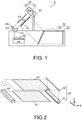
- FIG. 1 is a block diagram showing a configuration of the input device 1 of Embodiment 1.
- the input device 1 includes an optical sensor 10, an optical member 20, a display unit 30, a processing unit 40, an incidence suppression member 50, a first support member 61, and a second support member 62.
- the optical sensor 10 emits light traveling in a planar shape and senses an object on the plane where the emitted light travels. More specifically, the optical sensor 10 detects the position of an object on the plane where the emitted light travels.
- the optical sensor 10 may be implemented by an optical proximity sensor described in patent literature 2 for example, may be implemented by an optical operation device described in patent literature 3 for example, or may be implemented by other configurations.
- the optical sensor 10 is implemented by the optical proximity sensor described in patent literature 2.
- the optical member 20 changes a path of the light emitted from the optical sensor 10. More specifically, the optical member 20 includes a first optical element 21 which changes the path of light and a second optical element 22 which changes the path of light.
- the first optical element 21 and the second optical element 22 may be implemented by, for example, a mirror, a prism, or other configurations.
- the first optical element 21 and the second optical element 22 are configured by mirrors.
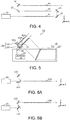
- FIG. 2 is a schematic diagram showing a state in which the optical member 20 changes the path of the light emitted from the optical sensor 10.
- the first optical element 21 has a mirror surface that is tilted 45 degrees to the positive direction of a Z-axis from a plane defined by an X-axis direction and a Y-axis direction shown in FIG. 2 .
- the second optical element 22 has a mirror surface that is tilted 135 degrees to the positive direction of the Z-axis from the plane defined by the X-axis direction and the Y-axis direction shown in FIG. 2 .
- the optical sensor 10 emits light traveling in a planar shape in the positive direction of the X-axis on the plane defined by the X-axis direction and the Y-axis direction shown in FIG. 2 .
- the light emitted from the optical sensor 10 is reflected by the first optical element 21, and travels in the positive direction of the Z-axis on a plane defined by the Z-axis direction and the Y-axis direction shown in FIG. 2 . That is, the path of the light emitted from the optical sensor 10 and traveling in a planar shape is changed from the positive direction of the X-axis to the positive direction of the Z-axis by the first optical element 21. Then, the light whose path has been changed by the first optical element 21 is reflected by the second optical element 22, and travels in the negative direction of the X-axis on the plane defined by the X-axis direction and the Y-axis direction shown in FIG. 2 . That is, the path of the light traveling in a planar shape whose path has been changed by the first optical element 21 is changed from the positive direction of the Z-axis to the negative direction of the X-axis by the second optical element 22.
- the optical sensor 10 and the optical member 20 form a first sensing surface 41 and a second sensing surface 42, the first sensing surface 41 consisting of a plane on which the light emitted from the optical sensor 10 whose path has not been changed by the optical member 20 travels, the second sensing surface 42 consisting of a plane on which the light emitted from the optical sensor 10 whose path has been changed one or more times (twice in this embodiment) by the optical member 20 travels.
- the second sensing surface 42 is located farther from the optical sensor 10 than the first sensing surface 41.
- the first sensing surface 41 and the second sensing surface 42 are both planes defined by the X-axis direction and the Y-axis direction shown in FIG. 2 . Therefore, the first sensing surface 41 and the second sensing surface 42 are substantially parallel to each other.
- the position of the first sensing surface 41 in the Z-axis direction shown in FIG. 2 is set as z1
- the position of the second sensing surface 42 in the Z-axis direction is set as z2.
- the display unit 30 displays an image on the display surface 31. More specifically, the display unit 30 includes a display 32 and an aerial imaging optical element 33, and the aerial imaging optical element 33 is used to perform aerial imaging on the image output from the display 32 to thereby display the image on the surface 31.
- the display unit 30 is not necessarily limited to the above configuration as long as it can display the image on the display surface 31.
- the display unit 30 may also be implemented by a configuration in which the display unit 30 includes a display, a half mirror and a retroreflective sheet, and the half mirror and the retroreflective sheet are used to perform aerial imaging on the image output from the display by a retroreflective method to thereby display the image on the display surface 31.
- the display surface 31 is substantially parallel to at least one of the first sensing surface 41 and the second sensing surface 42.
- the display surface 31 is substantially parallel to the first sensing surface 41 and the second sensing surface 42.
- the display surface 31 may be formed on the first sensing surface 41 or the second sensing surface.
- the incidence suppression member 50 is disposed on the path of the light whose path has been changed by the optical member 20, and suppresses the light whose path has been changed by the optical member 20 from being directly incident on the optical sensor 10 without contacting the object to be sensed. That is, the incidence suppression member 50 suppresses the light emitted from the optical sensor 10 from being incident on the optical sensor 10 without contacting the object to be sensed.
- the incidence suppression member 50 may be implemented by, for example, a light absorption material that absorbs light in a frequency band of the light emitted from the optical sensor 10, a mirror that reflects light in a direction in which the light is not incident on the optical sensor 10, or other configurations.
- the first support member 61 is a member that supports the optical member 20.
- the second support member 62 is a member that supports the incidence suppressing member 50.
- the processing unit 40 performs input processing based on the first sensing result of the optical sensor 10 on the first sensing surface 41 and the second sensing result of the optical sensor 10 on the second sensing surface 42.
- the processing unit 40 may include a processor and a memory and perform the input processing by the processor executing a program stored in the memory.
- click input processing for receiving a click operation of clicking an icon displayed on the display surface 31 from the user who uses the input device 1 is described with reference to the drawings.
- the display surface 31 is substantially parallel to the first sensing surface 41 and the second sensing surface 42, and the position of the display surface 31 in the Z-axis direction shown in FIG. 2 is z0.
- the display surface 31 is not necessarily limited to the example in which the display surface 31 is substantially parallel to the first sensing surface 41 and the second sensing surface 42.
- FIG. 3A and FIG. 3B are schematic diagrams showing a state in which the user uses a finger to perform the click operation.
- FIG. 3A is a schematic diagram at time t0
- FIG. 3B is a schematic diagram at time t1 (t1>t0).
- the display unit 30 displays an icon 70 to be clicked on the display surface 31 during the click input processing.
- the optical sensor 10 detects an X-axis coordinate x2 and a Y-axis coordinate y2 indicating the position of the finger 90 on the second sensing surface 42. Then, the processing unit 40 acquires the x2 and y2 detected by the optical sensor 10. Then, the processing unit 40 stores the acquired x2 and y2 in association with z2 indicating the position of the second sensing surface 42 in the Z-axis direction. At this time, the processing unit 40 may display a graphic 80A indicating the finger 90 at a position on the display surface 31 corresponding to the acquired x2 and y2.
- the processing unit 40 may output a sound indicating that the finger 90 enters the second sensing surface 42. In this way, by notifying the user that the click input processing is started through vision, hearing or the like, the user can recognize that the input processing is started.
- the optical sensor 10 detects an X-axis coordinate x1 and a Y-axis coordinate y1 indicating the position of the finger 90 on the first sensing surface 41. Then, the processing unit 40 acquires the x1 and y1 detected by the optical sensor 10. Then, the processing unit 40 stores the acquired x1 and y1 in association with z1 indicating the position of the first sensing surface 41 in the Z-axis direction. At this time, the processing unit 40 may display a graphic 80B indicating the finger 90 at a position on the display surface 31 corresponding to the acquired x1 and y1.
- the processing unit 40 may output a sound indicating that the finger 90 enters the first sensing surface 41. In this way, by notifying the user that the finger 90 of the user is closer to the input device 1 through vision, hearing or the like, the user can pay attention not to touch the input device 1 with the finger 90 or the like.
- the processing unit 40 estimates the position on the display surface 31 to which the finger 90 points. More specifically, the processing unit 40 linearly complements and extends a first vector in which the position indicated by x2, y2, and z2 on the second sensing surface 42 is used as a start point and the position indicated by x1, y1, and z1 on the first sensing surface 41 is used as an end point so that the end point position is on the display surface 31 to perform the linear interpolation and extend, thereby calculating a second vector in which the position indicated by x2, y2, and z2 on the second sensing surface 42 is used as a start point and the position indicated by x0, y0, and z0 on the display surface 31 is used as an end point. Then, the X-axis coordinate x0 and the Y-axis coordinate y0 indicating the end point position of the second vector are estimated as the position on the display surface 31 to which the finger 90 points.
- the processing unit 40 determines that the finger 90 has clicked the icon 70. Then, the processing unit 40 receives the click operation performed by the user in which the icon 70 displayed on the display surface 31 is clicked.
- the click operation performed by the user using a finger is described as an example, but the click operation is not necessarily performed using a finger.
- the click operation may be performed using any object to be sensed by the optical sensor 10, for example, an indicator bar or a pen.
- the input device 1 having the above configuration, in addition to the position on the plane substantially parallel to the display surface 31, the position in a direction perpendicular to the display surface 31 of the object to be sensed by the optical sensor 10 can also be detected.
- the non-contact input operation can be precisely received.
- the input device of Variant 1 is configured from the input device 1 by changing the optical member 20 to an optical member of Variant 1. More specifically, the optical member of Variant 1 is changed and configured from the optical member 20 so as to further have a third optical element of Variant 1 that changes the path of the light and a fourth optical element of Variant 1 that changes the path of the light in addition to the first optical element 21 and the second optical element 22.
- the third optical element of Variant 1 and the fourth optical element of Variant 1 may be implemented by, for example, a mirror, a prism, or other configurations.
- the third optical element of Variant 1 and the fourth optical element of Variant 1 are configured by mirrors.
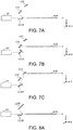
- FIG. 4 is a schematic diagram showing a state in which the optical member of Variant 1 changes the path of the light emitted from the optical sensor 10.
- the optical member of Variant 1 includes a third optical element 23 and a fourth optical element 24 in addition to the first optical element 21 and the second optical element 22.
- the third optical element 23 has a mirror surface that is tilted 45 degrees to the negative direction of the Z-axis from a plane defined by the X-axis direction and the Y-axis direction shown in FIG. 4 .
- the fourth optical element 24 has a mirror surface that is tilted 135 degrees to the negative direction of the Z-axis from the plane defined by the X-axis direction and the Y-axis direction shown in FIG. 4 .
- the light whose path has been changed by the second optical element 21 is reflected by the third optical element 23, and travels in the positive direction of the Z-axis on the plane defined by the Z-axis direction and the Y-axis direction shown in FIG. 4 . That is, the path of the light emitted from the optical sensor 10 and traveling in a planar shape is changed from the negative direction of the X-axis to the positive direction of the Z-axis by the third optical element 23. Then, the light whose path has been changed by the third optical element 23 is reflected by the fourth optical element 24, and travels in the positive direction of the X-axis on the plane defined by the X-axis direction and the Y-axis direction shown in FIG. 4 . That is, the path of the light traveling in a planar shape whose path has been changed by the third optical element 23 is changed from the positive direction of the Z-axis to the positive direction of the X-axis by the fourth optical element 24.
- the optical sensor 10 and the optical member of Variant 1 further form a third sensing surface 43 consisting of a plane on which the light whose path has been changed one or more times (three times in this variant) by the optical member of Variant 1 travels. Therefore, the processing unit 40 can perform the input processing based further on a third sensing result of the optical sensor 10 on the sensing surface 43 in addition to the first sensing result of the optical sensor 10 on the first sensing surface 41 and the second sensing result of the optical sensor 10 on the second sensing surface 42.
- the non-contact input operation can be more precisely received.
- Embodiment 2 in which a part of the configuration is changed from the input device 1 of Embodiment 1 is described.
- FIG. 5 is a block diagram showing a configuration of an input device 1A of Embodiment 2.
- the same components of the input device 1A as those of the input device 1 are denoted by the same reference numerals and a detailed description thereof is omitted and regarded as already described, and differences from the input device 1 are mainly described.
- the input device 1A is different from the input device 1 of Embodiment 1 in that the optical member 20 is changed to an optical member 120, the first support member 61 is changed to a first support member 61A, and the incidence suppression member 50 and the second support member 62 are removed.
- the optical member 120 changes the path of the light emitted from the optical sensor 10. More specifically, the optical member 120 includes a rotatable first optical element 121 that changes the path of light and a second optical element 122 that changes the path of light.
- the first optical element 121 and the second optical element 122 may be implemented by, for example, a mirror, a prism, or other configurations.
- the first optical element 121 and the second optical element 122 are configured by mirrors.
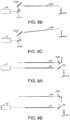
- FIGS. 6A and 6B are schematic diagrams showing a state in which the optical member 120 changes the path of the light emitted from the optical sensor 10.
- the first optical element 121 has a mirror surface, and can be rotated to a first angle at which the mirror surface is substantially parallel to a plane defined by the X-axis direction and the Y-axis direction shown in FIGS. 6A and 6B , and a second angle at which the mirror surface is substantially parallel to a plane tilted 45 degrees to the positive direction of the Z-axis from the plane defined by the X-axis direction and the Y-axis direction shown in FIGS. 6A and 6B .
- the second optical element 122 has a mirror surface that is tilted 135 degrees to the negative direction of the Z-axis from the plane defined by the X-axis direction and the Y-axis direction shown in FIGS. 6A and 6B .
- the optical sensor 10 and the optical member 120 form a first sensing surface 41A consisting of a plane on which the light emitted from the optical sensor 10 whose path has not been changed by the optical member 120 travels.
- the first optical element 121 when the first optical element 121 is at the second angle, the light emitted from the optical sensor 10 and traveling in a planar shape is reflected by the first optical element 121, and travels in the positive direction of the Z-axis on the plane defined by the Z-axis direction and the Y-axis direction shown in FIG. 6B . That is, the path of the light emitted from the optical sensor 10 and traveling in a planar shape is changed from the positive direction of the X-axis to the positive direction of the Z-axis by the first optical element 121.
- the light whose path has been changed by the first optical element 121 is reflected by the second optical element 122, and travels in the positive direction of the X-axis on the plane defined by the X-axis direction and the Y-axis direction shown in FIG. 6B . That is, the path of the light traveling in a planar shape whose path has been changed by the first optical element 121 is changed by the second optical element 122 from the positive direction of the Z-axis to the positive direction of the X-axis. Therefore, the optical sensor 10 and the optical member 120 form a second sensing surface 42A consisting of a plane on which the light emitted from the optical sensor 10 whose path has been changed one or more times by the optical member 20 travels.
- the optical sensor 10 and the optical member 120 form the first sensing surface 41A and the second sensing surface 42A by a time-division of a first period in which the first optical element 121 is at the first angle and a second period in which the first optical element 121 is at the second angle.
- the first support member 61A is a member that supports the optical member 120.
- the input device 1A having the above configuration, similar to Embodiment 1, in addition to the position of the object to be sensed by the optical sensor 10 on the plane substantially parallel to the display surface 31, the position in a direction perpendicular to the display surface 31 can also be detected. Thus, according to the input device 1A, the non-contact input operation can be precisely received.
- the optical member 120 and the first support member 61A are disposed in front of the first sensing surface 41A when viewed from the optical sensor 10. Thereby, according to the input device 1A, it is possible to reduce the frequency at which the user comes into contact with the input device 1A when the user who uses the input device 1A performs an input operation.
- the input device of Variant 2 is configured from the input device 1A by changing the optical member 120 to an optical member of Variant 2. More specifically, the optical member of Variant 2 is configured from the optical member 120 by changing the first optical element 121 to a rotatable first optical element of Variant 2 that changes the path of light and further changing to have a third optical element of Variant 2 that changes the path of light.
- the first optical element of Variant 2 and the third optical element of Variant 2 may be implemented by, for example, a mirror, a prism, or other configurations.
- the first optical element of Variant 2 and the third optical element of Variant 2 are configured by mirrors.
- FIGS. 7A to 7C are schematic diagrams showing a state in which the optical member of Variant 2 changes the path of the light emitted from the optical sensor 10.
- the optical member of Variant 2 includes a first optical element 121A and a third optical element 123 in addition to the second optical element 22.
- the first optical element 121A has a mirror surface, and can be rotated to a first angle at which the mirror surface is substantially parallel to a plane defined by the X-axis direction and the Y-axis direction shown in FIGS. 7A to 7C , a second angle at which the mirror surface is substantially parallel to a plane that is tilted 45 degrees to the positive direction of the Z-axis from the plane defined by the X-axis direction and the Y-axis direction shown in FIGS. 7A to 7C , and a third angle at which the mirror surface is substantially parallel to a plane that is tilted 35 degrees to the positive direction of the Z-axis from the plane defined by the X-axis direction and the Y-axis direction shown in FIGS. 7A to 7C .
- the third optical element 123 has a mirror surface that is tilted 145 degrees to the negative direction of the Z-axis from the plane defined by the X-axis direction and the Y-axis direction shown in FIGS. 7A to 7C .
- the optical sensor 10 and the optical member of Variant 2 form a first sensing surface 41A consisting of a plane on which the light emitted from the optical sensor 10 whose path has not been changed by the optical member of Variant 2 travels.
- the optical sensor 10 and the optical device of Variant 2 form a second sensing surface 42A consisting of a plane on which the light emitted from the optical sensor 10 whose path has been changed one or more times (twice in this variant) by the optical member of Variant 2 travels.
- the first optical element 121A when the first optical element 121A is at the third angle, the light emitted from the optical sensor 10 and traveling in a planar shape is reflected by the first optical element 121A, and travels in a first direction on the positive side of the Z-axis on a first plane that is tilted 70 degrees to the positive direction of the Z-axis from the plane defined by the X-axis direction and the Y-axis direction shown in FIG. 7C . That is, the path of the light emitted from the optical sensor 10 and traveling in a planar shape is changed from the positive direction of the X-axis to the first direction on the first plane by the first optical element 121A.
- the light whose path has been changed by the first optical element 121A is reflected by the third optical element 123, and travels in the positive direction of the X-axis on the plane defined by the X-axis direction and the Y-axis direction shown in FIG. 7C . That is, the path of the light traveling in a planar shape whose path has been changed by the first optical element 121 is changed by the third optical element 123 from the first direction on the first plane to the positive direction of the X-axis.
- the optical sensor 10 and the optical member of Variant 2 form a third sensing surface 43A consisting of a plane on which the light emitted from the optical sensor 10 whose path has been changed one or more times (twice in this variant) by the optical member of Variant 2 travels.
- the optical sensor 10 and the optical member of Variant 2 form the first sensing surface 41A, the second sensing surface 42A, and the third sensing surface 43A by a time-division of a first period in which the first optical element 121A is at the first angle, a second period in which the first optical element 121A is at the second angle, and a third period in which the first optical element 121A is at the third angle. Therefore, the processing unit 40 can perform the input processing based further on a third sensing result of the optical sensor 10 on the third sensing surface 43A in addition to the first sensing result of the optical sensor 10 on the first sensing surface 41A and the second sensing result of the optical sensor 10 on the second sensing surface 42A.
- the non-contact input operation can be more precisely received.
- the input device of Variant 3 is configured from the input device 1A by changing the optical member 120 to an optical member of Variant 3. More specifically, the optical member of Variant 3 is configured from the optical member 120 by changing the first optical element 121 to a rotatable first optical element of Variant 3 that changes the path of light and changing the second optical element 122 to a second optical element of Variant 3 that changes the path of light.
- the first optical element of Variant 3 and the second optical element of Variant 3 may be implemented by, for example, a mirror, a prism, or other configurations. Here, as an example, the first optical element of Variant 3 and the second optical element of Variant 3 are configured by mirrors.
- FIGS. 8A to 8C are schematic diagrams showing a state in which the optical member of Variant 3 changes the path of the light emitted from the optical sensor 10.
- the optical member of Variant 3 includes a first optical element 121B and a second optical element 122B.
- the first optical element 121B has a mirror surface, and can be rotated to a first angle at which the mirror surface is substantially parallel to a plane defined by the X-axis direction and the Y-axis direction shown in FIGS. 8A to 8C , a second angle at which the mirror surface is substantially parallel to a plane that is tilted 45 degrees to the positive direction of the Z-axis from the plane defined by the X-axis direction and the Y-axis direction shown in FIGS. 8A to 8C , and a third angle at which the mirror surface is substantially parallel to a plane that is tilted 40 degrees to the positive direction of the Z-axis from the plane defined by the X-axis direction and the Y-axis direction shown in FIGS. 8A to 8C .
- the second optical element 122B has the same configuration as that of the second optical element 122 of Embodiment 2 except that the mirror surface area of the second optical element 122B is increased. That is, the second optical element 122B is configured from the second optical element 122 of Embodiment 2 in a manner that the mirror surface area of the second optical element 122B is increased.
- the optical sensor 10 and the optical member of Variant 3 form a first sensing surface 41A consisting of a plane on which the light emitted from the optical sensor 10 whose path has not been changed by the optical member of Variant 3 travels.
- the optical sensor 10 and the optical device of Variant 3 form a second sensing surface 42A consisting of a plane on which the light emitted from the optical sensor 10 whose path has been changed one or more times by the optical member of Variant 3 travels.
- the first optical element 121B when the first optical element 121B is at the third angle, the light emitted from the optical sensor 10 and traveling in a planar shape is reflected by the first optical element 121B, and travels in a first direction on the positive side of the Z-axis on a second plane that is tilted 80 degrees to the positive direction of the Z-axis from the plane defined by the X-axis direction and the Y-axis direction shown in FIG. 8C . That is, the path of the light emitted from the optical sensor 10 and traveling in a planar shape is changed from the positive direction of the X-axis to the first direction on the second plane by the first optical element 121B.
- the light whose path has been changed by the first optical element 121B is reflected by the second optical element 122B, and travels in the first direction on the positive side of the Z-axis on a third plane that is tilted 10 degrees to the positive direction of the Z-axis from the plane defined by the X-axis direction and the Y-axis direction shown in FIG. 8C . That is, the path of the light traveling in a planar shape whose path has been changed by the first optical element 121 is changed from the first direction on the second plane to the first direction on the third plane by the second optical element 122B.
- the optical sensor 10 and the optical member of Variant 3 form a third sensing surface 43B consisting of a plane on which the light emitted from the optical sensor 10 whose path has been changed one or more times (twice in this variant) by the optical member of Variant 3 travels.
- the optical sensor 10 and the optical member of Variant 3 form the first sensing surface 41A, the second sensing surface 42A, and the third sensing surface 43B by a time-division of a first period in which the first optical element 121B is at the first angle, a second period in which the first optical element 121B is at the second angle, and a third period in which the first optical element 121B is at the third angle. Therefore, the processing unit 40 can perform the input processing based further on a third sensing result of the optical sensor 10 on the third sensing surface 43B in addition to the first sensing result of the optical sensor 10 on the first sensing surface 41A and the second sensing result of the optical sensor 10 on the second sensing surface 42A.
- the non-contact input operation can be more precisely received.
- the input device of Variant 4 is configured from the input device 1 by changing the optical member 20 to an optical member of Variant 4. More specifically, the optical member of Variant 4 is configured from the optical member 20 by changing the second optical element 22 to a movable second optical element of Variant 4 that changes the path of light.
- the second optical element of Variant 4 may be implemented by, for example, a mirror, a prism, or other configurations. Here, as an example, the second optical element of Variant 4 is configured by a mirror.
- FIGS. 9A and 9B are schematic diagrams showing a state in which the optical member of Variant 4 changes the path of the light emitted from the optical sensor 10.
- the optical member of Variant 4 includes a second optical element 22A in addition to the first optical element 21.
- the second optical element 22A has a mirror surface that is tilted 135 degrees to the positive direction of the Z-axis from a plane defined by the X-axis direction and the Y-axis direction shown in FIGS. 9A and 9B , and can slide in the Z-axis direction between a first position (the position of the second optical element 22A in FIG. 9A ) and a second position (the position of the second optical element 22A in FIG. 9B ) on the same plane defined by the X-axis direction and the Y-axis direction.
- the optical sensor 10 and the optical member of Variant 4 form the first sensing surface 41 and the second sensing surface 42.
- the second optical element 22A when the second optical element 22A is at the second position, the light emitted from the optical sensor 10 and traveling in a planar shape is reflected by the first optical element 21, and travels in the positive direction of the Z-axis on the plane defined by the Z-axis direction and the Y-axis direction shown in FIG. 9B . That is, the path of the light emitted from the optical sensor 10 and traveling in a planar shape is changed from the positive direction of the X-axis to the positive direction of the Z-axis by the first optical element 21.
- the light whose path has been changed by the first optical element 21 is reflected by the second optical element 22A, and travels in the negative direction of the X-axis on the plane defined by the X-axis direction and the Y-axis direction shown in FIG. 9B . That is, the light traveling in a planar shape whose path has been changed by the first optical element 21 is changed from the positive direction of the Z-axis to the negative direction of the X-axis by the second optical element 22A. Therefore, the optical sensor 10 and the optical member of Variant 4 form a third sensing surface 43C consisting of a plane on which the light emitted from the optical sensor 10 whose path has been changed one or more times by the optical member of Variant 4 travels.
- the optical sensor 10 and the optical member of Variant 4 constantly form the first sensing surface 41, and also form the second sensing surface 42 and the third sensing surface 43C by a time-division of a first period in which the second optical element 22A is at the first position and a second period in which the second optical element 22A is at the second position. Therefore, the processing unit 40 can perform the input processing based further on a third sensing result of the optical sensor 10 on the third sensing surface 43C in addition to the first sensing result of the optical sensor 10 on the first sensing surface 41 and the second sensing result of the optical sensor 10 on the second sensing surface 42.
- the non-contact input operation can be more precisely received.
- the input device of Variant 5 is configured from the input device 1 by changing the optical member 20 to an optical member of Variant 5. More specifically, the optical member of Variant 5 is configured from the optical member 20 by removing the second optical element 22 and changing the first optical element 21 to a rotatable first optical element of Variant 5 that changes the path of light.
- the first optical element of Variant 5 may be implemented by, for example, a mirror, a prism, or other configurations. Here, as an example, the first optical element of Variant 5 is configured by a mirror.
- FIGS. 10A to 10C are schematic diagrams showing a state in which the optical member of Variant 5 changes the path of the light emitted from the optical sensor 10.
- the optical member of Variant 5 includes a first optical element 21B.
- the first optical element 21B has a mirror surface, and can be rotated to a first angle at which the mirror surface is substantially parallel to a plane defined by the X-axis direction and the Y-axis direction shown in FIGS. 10A to 10C , a second angle at which the mirror surface is substantially parallel to a plane that is tilted 70 degrees to the positive direction of the Z-axis from a plane defined by the X-axis direction and the Y-axis direction shown in FIGS. 10A to 10C , and a third angle at which the mirror surface is substantially parallel to a plane that is tilted 80 degrees to the positive direction of the Z-axis from the plane defined by the X-axis direction and the Y-axis direction shown in FIGS. 10A to 10C .
- the optical sensor 10 and the optical member of Variant 5 form a first sensing surface 41 consisting of a plane on which the light emitted from the optical sensor 10 whose path has not been changed by the optical member of Variant 5 travels.
- the light emitted from the optical sensor 10 is reflected by the first optical element 21B, and travels in the first direction on the positive direction side of the Z-axis on a fourth plane that is tilted 140 degrees to the positive direction of the Z-axis from the plane defined by the X-axis direction and the Y-axis direction shown in FIG. 10B . That is, the path of the light emitted from the optical sensor 10 and traveling in a planar shape is changed from the positive direction of the X-axis to the first direction on the fourth plane by the first optical element 21B.
- the optical sensor 10 and the optical member of Variant 5 form a second sensing surface 42D consisting of a plane on which the light emitted from the optical sensor 10 whose path has been changed one or more times (once in this variant) by the optical member of Variant 5 travels.
- the light emitted from the optical sensor 10 is reflected by the first optical element 21B, and travels in the first direction on the positive direction side of the Z-axis on a fifth plane that is tilted 160 degrees to the positive direction of the Z-axis from the plane defined by the X-axis direction and the Y-axis direction shown in FIG. 10C . That is, the path of the light emitted from the optical sensor 10 and traveling in a planar shape is changed from the positive direction of the X-axis to the first direction on the fifth plane by the first optical element 21B.
- the optical sensor 10 and the optical member of Variant 5 form a third sensing surface 43D consisting of a plane on which the light emitted from the optical sensor 10 whose path has been changed one or more times (once in this variant) by the optical member of Variant 5 travels.
- the optical sensor 10 and the optical member of Variant 5 constantly form the first sensing surface 41, and also form the second sensing surface 42D and the third sensing surface 43D by a time-division of a first period in which the first optical element 21B is at the first position and a second period in which the first optical element 21B is at the second position. Therefore, the processing unit 40 can perform the input processing based further on a third sensing result of the optical sensor 10 on the third sensing surface 43D in addition to the first sensing result of the optical sensor 10 on the first sensing surface 41 and the second sensing result of the optical sensor 10 on the second sensing surface 42D.
- the non-contact input operation can be more precisely received.
- the input device of Variant 6 is configured from the input device 1A by changing the optical member 120 to an optical member of Variant 6. More specifically, the optical member of Variant 6 is configured from the optical member 120 by removing the second optical element 122 and changing the first optical element 121 to a rotatable first optical element of Variant 6 that changes the path of light.
- the first optical element of Variant 6 may be implemented by, for example, a mirror, a prism, or other configurations. Here, as an example, the first optical element of Variant 6 is configured by a mirror.
- FIGS. 11A to 11C are schematic diagrams showing a state in which the optical member of Variant 6 changes the path of the light emitted from the optical sensor 10.
- the optical member of Variant 6 includes a first optical element 121C.
- the first optical element 121C has a mirror surface, and can be rotated to a first angle at which the mirror surface is substantially parallel to a plane defined by the X-axis direction and the Y-axis direction shown in FIGS. 11A to 11C , a second angle at which the mirror surface is substantially parallel to a plane that is tilted 10 degrees to the positive direction of the Z-axis from the plane defined by the X-axis direction and the Y-axis direction shown in FIGS. 11A to 11C , and a third angle at which the mirror surface is substantially parallel to a plane that is tilted 20 degrees to the positive direction of the Z-axis from the plane defined by the X-axis direction and the Y-axis direction shown in FIGS. 11A to 11C .
- the optical sensor 10 and the optical member of Variant 6 form a first sensing surface 41A consisting of a plane on which the light emitted from the optical sensor 10 whose path has not been changed by the optical member of Variant 6 travels.
- the first optical element 121C when the first optical element 121C is at the second angle, the light emitted from the optical sensor 10 and traveling in a planar shape is reflected by the first optical element 121C, and travels in the first direction on the positive side of the Z-axis on a sixth plane that is tilted 20 degrees to the positive direction of the Z-axis from the plane defined by the X-axis direction and the Y-axis direction shown in FIG. 11B . That is, the path of the light emitted from the optical sensor 10 and traveling in a planar shape is changed from the positive direction of the X-axis to the first direction on the sixth plane by the first optical element 121C.
- the optical sensor 10 and the optical member of Variant 6 form a second sensing surface 42E consisting of a plane on which the light emitted from the optical sensor 10 whose path has been changed one or more times (once in this variant) by the optical member of Variant 6 travels.
- the first optical element 121C when the first optical element 121C is at the third angle, the light emitted from the optical sensor 10 and traveling in a planar shape is reflected by the first optical element 121C, and travels in the first direction on the positive side of the Z-axis on a seventh plane that is tilted 40 degrees to the positive direction of the Z-axis from the plane defined by the X-axis direction and the Y-axis direction shown in FIG. 11C . That is, the path of the light emitted from the optical sensor 10 and traveling in a planar shape is changed from the positive direction of the X-axis to the first direction on the seventh plane by the first optical element 121C.
- the optical sensor 10 and the optical member of Variant 6 form a third sensing surface 43E consisting of a plane on which the light emitted from the optical sensor 10 whose path has been changed one or more times (once in this variant) by the optical member of Variant 6 travels.
- the optical sensor 10 and the optical member of Variant 6 constantly form the first sensing surface 41A, and also form the second sensing surface 42E and the third sensing surface 43E by a time-division of a first period in which the first optical element 121C is at the first position and a second period in which the first optical element 121C is at the second position. Therefore, the processing unit 40 can perform the input processing based further on a third sensing result of the optical sensor 10 on the third sensing surface 43E in addition to the first sensing result of the optical sensor 10 on the first sensing surface 41A and the second sensing result of the optical sensor 10 on the second sensing surface 42E.
- the non-contact input operation can be more precisely received.
- the input device of Embodiment 1 has a configuration in which the first optical element 21 has a mirror surface that is tilted 45 degrees to the positive direction of the Z-axis from the plane defined by the X-axis direction and the Y-axis direction shown in FIG. 2 , and the second optical element 22 has a mirror surface that is tilted 135 degrees to the positive direction of the Z-axis from the plane defined by the X-axis direction and the Y-axis direction shown in FIG. 2 .
- the input device of Variant 7 has a configuration in which a first optical element of Variant 7 has a mirror surface that is tilted 45 degrees to the positive direction of the Z-axis from the plane defined by the X-axis direction and the Y-axis direction shown in FIG. 2 and further rotated counterclockwise by an angle ⁇ about the Z-axis, and a second optical element of Variant 7 has a mirror surface that is tilted 135 degrees to the positive direction of the Z-axis from the plane defined by the X-axis direction and the Y-axis direction shown in FIG. 2 and further rotated counterclockwise by the angle ⁇ about the Z-axis.
- FIG. 12 is a schematic diagram showing a state in which the optical member of Variant 7 changes the path of the light emitted from the optical sensor 10.
- the optical member of Variant 7 includes a first optical element 21F and a second optical element 22F.
- the optical sensor 10 emits the light traveling in a planar shape in the positive direction of the X-axis on a plane defined by the X-axis direction and the Y-axis direction shown in FIG. 12 . Therefore, similar to the input device 1 of Embodiment 1, the optical sensor 10 and the optical member of Variant 7 form the first sensing surface 41.
- the light emitted from the optical sensor 10 and traveling in a planar shape is reflected by the first optical element 21F and the second optical element 22F, and travels in a direction tilted by an angle 2 ⁇ counterclockwise from the X-axis direction on the plane defined by the X-axis direction and the Y-axis direction shown in FIG. 2 . Therefore, the optical sensor 10 and the optical member of Variant 7 form a second sensing surface 42F from the light traveling in the direction tilted by the angle 2 ⁇ counterclockwise from the X-axis direction on the plane defined by the X-axis direction and the Y-axis direction shown in FIG. 2 .
- a second object that cannot be sensed by the optical sensor 10 on the first sensing surface 41 due to occlusion of the first object can be sensed by the optical sensor 10 on the second sensing surface 42F.
- Embodiment 3 in which a part of the configuration is changed from the input device 1 of Embodiment 1 is described.
- FIG. 13 is a block diagram showing a configuration of an input device 1B of Embodiment 3.
- the same components of the input device 1B as those of the input device 1 are denoted by the same reference numerals and a detailed description thereof is omitted as already described, and differences from the input device 1 are mainly described.
- the input device 1B is different from the input device 1 of Embodiment 1 in that the display unit 30 is changed to a display unit 30A.
- the display unit 30A displays an image on a display surface 31A without aerial imaging.
- the display unit 30A may be implemented by, for example, a liquid crystal display using a liquid crystal surface thereof as the display surface 31A, a projector that projects an image on a screen serving as the display surface 31A, or other configurations.
- the display unit 30A is disposed in a manner that the display surface 31A is closer to the main body side of the input device 1B than the first sensing surface 41 and the second sensing surface 42. Thereby, a user who uses the input device 1B can perform an input operation without touching the display unit 30A.
- the display surface 31A is substantially parallel to at least one of the first sensing surface 41 and the second sensing surface 42.
- the display surface 31A is substantially parallel to the first sensing surface 41 and the second sensing surface 42.
- the input device 1B having the above configuration, similar to Embodiment 1, in addition to the position of the object to be sensed by the optical sensor 10 on the plane substantially parallel to the display surface 31A, the position in a direction perpendicular to the display surface 31A can also be detected. Thus, according to the input device 1B, the non-contact input operation can be precisely received.
- the image is displayed on the display surface 31A without aerial imaging. Accordingly, the input device 1B can be implemented by a relatively simple configuration.
- the input device of the disclosure is described above based on Embodiments 1 to 3 and Variants 1 to 7, but the disclosure is limited to these embodiments and variants. Configurations obtained by applying various modification conceived by those skilled in the art to the above embodiments or variants in a range not departing from the gist of the disclosure, or forms configured by combining the components in different embodiments or variants may be included in the scope of the aspect of the disclosure.
- the disclosure can be widely used in devices capable of performing a non-contact input operation.
Landscapes
- Engineering & Computer Science (AREA)
- General Engineering & Computer Science (AREA)
- Theoretical Computer Science (AREA)
- Physics & Mathematics (AREA)
- General Physics & Mathematics (AREA)
- Human Computer Interaction (AREA)
- Spectroscopy & Molecular Physics (AREA)
- Position Input By Displaying (AREA)
- User Interface Of Digital Computer (AREA)
Abstract
Description
- The disclosure relates to an input device.
- Conventionally, an input device in which aerial imaging and a sensor are combined and which is capable of performing a non-contact input operation is known (for example, see patent literature 1).
-
- [Patent literature 1] Japanese Patent Laid-open No.
2018-88027 - [Patent literature 2] Japanese Patent No.
6029640 - [Patent literature 3] Japanese Patent No.
5229704 - In the conventional input device described in patent literature 1, it is difficult to precisely detect the position of an object to be detected by the sensor in a direction perpendicular to a plane on which an aerial image is displayed. Therefore, in the above conventional input device, there is a constant limit in the precision for receiving the non-contact input operation.
- In order to achieve the input device of one aspect of the disclosure includes an optical sensor which emits light traveling in a planar shape and senses an object on the plane where the emitted light travels, an optical member which changes a path of the light emitted from the optical sensor, and a processing unit which performs input processing based on sensing results of the optical sensor; the optical sensor and the optical member form a first sensing surface consisting of a planar region in which the light emitted from the optical sensor travels and a second sensing surface that is farther from the optical sensor than the first sensing surface, and the processing unit performs the input processing based on a first sensing result of the optical sensor on the first sensing surface and a second sensing result of the optical sensor on the second sensing surface.
-
-
FIG. 1 is a block diagram showing a configuration of an input device of Embodiment 1. -
FIG. 2 is a schematic diagram showing a state in which an optical member of Embodiment 1 changes a path of light emitted from an optical sensor of Embodiment 1. -
FIG. 3A is a schematic diagram showing a state in which a user uses a finger to perform a click operation. -
FIG. 3B is a schematic diagram showing a state in which the user uses a finger to perform the click operation. -
FIG. 4 is a schematic diagram showing a state in which an optical member of Variant 1 changes a path of light emitted from an optical sensor of Variant 1. -
FIG. 5 is a block diagram showing a configuration of an input device of Embodiment 2. -
FIG. 6A is a schematic diagram showing a state in which an optical member of Embodiment 2 changes a path of light emitted from an optical sensor of Embodiment 2. -
FIG. 6B is a schematic diagram showing a state in which the optical member of Embodiment 2 changes the path of the light emitted from the optical sensor of Embodiment 2. -
FIG. 7A is a schematic diagram showing a state in which an optical member of Variant 2 changes a path of light emitted from an optical sensor of Variant 2. -
FIG. 7B is a schematic diagram showing a state in which the optical member of Variant 2 changes the path of the light emitted from the optical sensor of Variant 2. -
FIG. 7C is a schematic diagram showing a state in which the optical member of Variant 2 changes the path of the light emitted from the optical sensor of Variant 2. -
FIG. 8A is a schematic diagram showing a state in which an optical member of Variant 3 changes a path of light emitted from an optical sensor of Variant 3. -
FIG. 8B is a schematic diagram showing a state in which the optical member of Variant 3 changes the path of the light emitted from the optical sensor of Variant 3. -
FIG. 8C is a schematic diagram showing a state in which the optical member of Variant 3 changes the path of the light emitted from the optical sensor of Variant 3. -
FIG. 9A is a schematic diagram showing a state in which an optical member of Variant 4 changes a path of light emitted from an optical sensor of Variant 4. -
FIG. 9B is a schematic diagram showing a state in which the optical member of Variant 4 changes the path of the light emitted from the optical sensor of Variant 4. -
FIG. 10A is a schematic diagram showing a state in which an optical member of Variant 5 changes a path of light emitted from an optical sensor of Variant 5. -
FIG. 10B is a schematic diagram showing a state in which the optical member of Variant 5 changes the path of the light emitted from the optical sensor of Variant 5. -
FIG. 10C is a schematic diagram showing a state in which the optical member of Variant 5 changes the path of the light emitted from the optical sensor of Variant 5. -
FIG. 11A is a schematic diagram showing a state in which an optical member of Variant 6 changes a path of light emitted from an optical sensor of Variant 6. -
FIG. 11B is a schematic diagram showing a state in which the optical member of Variant 6 changes the path of the light emitted from the optical sensor of Variant 6. -
FIG. 11C is a schematic diagram showing a state in which the optical member of Variant 6 changes the path of the light emitted from the optical sensor of Variant 6 -
FIG. 12 is a schematic diagram showing a state in which an optical member of Variant 7 changes a path of light emitted from an optical sensor of Variant 7. -
FIG. 13 is a block diagram showing a configuration of an input device of Embodiment 3. - One of the embodiments of the disclosure is to provide an input device capable of precisely receiving a non-contact input operation.
- According to the input device having the above configuration, in addition to the position of the object to be sensed by the optical sensor on a plane substantially parallel to a display surface, the position in a direction perpendicular to the display surface can also be detected.
- Thus, according to the input device having the above configuration, the non-contact input operation can be precisely received.
- For example, the light traveling on the second sensing surface may be the light traveling on the first sensing surface whose path has been changed by the optical member.
- Thereby, the first sensing surface and the second sensing surface can be formed simultaneously.
- For example, the optical member may include a rotatable optical element capable of changing the path of the light emitted from the optical sensor; the first sensing surface may be formed when the rotation angle of the optical element is a first angle, and the second sensing surface may be formed when the rotation angle of the optical element is a second angle.
- Thereby, the first sensing surface and the second sensing surface can be formed by controlling the rotation angle of the optical element.
- For example, the optical member may include a movable optical element capable of changing the path of the light emitted from the optical sensor; the first sensing surface may be formed when the position of the optical element is a first position, and the second sensing surface may be formed when the position of the optical element is a second position.
- Thereby, the first sensing surface and the second sensing surface can be formed by controlling the position of the optical element.
- For example, the first sensing surface and the second sensing surface may be substantially parallel. Here, "substantially parallel" refers to not only a strictly parallel state but also an essentially parallel state.
- Thereby, the position of the object to be sensed by the optical sensor in the direction perpendicular to the display surface can be more precisely detected.
- For example, the optical member may include a mirror.
- Thereby, an optical member can be implemented by a relatively simple configuration.
- For example, a display unit which displays an image on the display surface may be further included.
- Thereby, the display surface can be displayed.
- For example, the display surface may be substantially parallel to at least one of the first sensing surface and the second sensing surface.
- Thereby, the sensing precision of the optical sensor can be improved.
- For example, the display unit may display the image on the display surface by aerial imaging, and the display surface may be formed on the first sensing surface or the second sensing surface.
- Thereby, the frequency at which a user performing the input operation comes into contact with the display unit can be reduced.
- For example, an incidence suppression member which suppresses the light emitted from the optical sensor from being incident on the optical sensor without contacting the object to be sensed may be further included.
- Thereby, the sensing precision of the optical sensor can be improved.
- For example, the display unit may include an icon in the displayed image, and the processing unit may detect, based on the first sensing result and the second sensing result, a click movement of clicking the icon from a user who uses the input device and perform the input processing based on the detection.
- Thereby, the input operation performed by the movement of clicking the icon from the user can be received.
- According to the disclosure, an input device capable of precisely receiving a non-contact input operation is provided.
- Hereinafter, embodiments of the disclosure are described in detail with reference to the drawings. Besides, each of the embodiments described below shows a comprehensive or specific example. Numerical values, shapes, materials, components, arrangement positions and connection forms of the components, and the like shown in the following embodiments are merely examples and are not intended to limit the disclosure. In addition, components not described in the independent claims within the components in the following embodiments are described as arbitrary components.
- An input device of Embodiment 1 is described below with reference to the drawings. The input device displays an image formed by aerial imaging, and receives a non-contact input operation on the displayed image from a user who uses the input device.
-
FIG. 1 is a block diagram showing a configuration of the input device 1 of Embodiment 1. - As shown in
FIG. 1 , the input device 1 includes anoptical sensor 10, anoptical member 20, adisplay unit 30, aprocessing unit 40, anincidence suppression member 50, afirst support member 61, and asecond support member 62. - The
optical sensor 10 emits light traveling in a planar shape and senses an object on the plane where the emitted light travels. More specifically, theoptical sensor 10 detects the position of an object on the plane where the emitted light travels. Theoptical sensor 10 may be implemented by an optical proximity sensor described in patent literature 2 for example, may be implemented by an optical operation device described in patent literature 3 for example, or may be implemented by other configurations. Here, as an example, theoptical sensor 10 is implemented by the optical proximity sensor described in patent literature 2. - The
optical member 20 changes a path of the light emitted from theoptical sensor 10. More specifically, theoptical member 20 includes a firstoptical element 21 which changes the path of light and a secondoptical element 22 which changes the path of light. The firstoptical element 21 and the secondoptical element 22 may be implemented by, for example, a mirror, a prism, or other configurations. Here, as an example, the firstoptical element 21 and the secondoptical element 22 are configured by mirrors. -
FIG. 2 is a schematic diagram showing a state in which theoptical member 20 changes the path of the light emitted from theoptical sensor 10. - As shown in
FIG. 2 , the firstoptical element 21 has a mirror surface that is tilted 45 degrees to the positive direction of a Z-axis from a plane defined by an X-axis direction and a Y-axis direction shown inFIG. 2 . - The second
optical element 22 has a mirror surface that is tilted 135 degrees to the positive direction of the Z-axis from the plane defined by the X-axis direction and the Y-axis direction shown inFIG. 2 . - The
optical sensor 10 emits light traveling in a planar shape in the positive direction of the X-axis on the plane defined by the X-axis direction and the Y-axis direction shown inFIG. 2 . - As shown in
FIG. 2 , the light emitted from theoptical sensor 10 is reflected by the firstoptical element 21, and travels in the positive direction of the Z-axis on a plane defined by the Z-axis direction and the Y-axis direction shown inFIG. 2 . That is, the path of the light emitted from theoptical sensor 10 and traveling in a planar shape is changed from the positive direction of the X-axis to the positive direction of the Z-axis by the firstoptical element 21. Then, the light whose path has been changed by the firstoptical element 21 is reflected by the secondoptical element 22, and travels in the negative direction of the X-axis on the plane defined by the X-axis direction and the Y-axis direction shown inFIG. 2 . That is, the path of the light traveling in a planar shape whose path has been changed by the firstoptical element 21 is changed from the positive direction of the Z-axis to the negative direction of the X-axis by the secondoptical element 22. - As shown in
FIGS. 1 and 2 , theoptical sensor 10 and theoptical member 20 form afirst sensing surface 41 and asecond sensing surface 42, thefirst sensing surface 41 consisting of a plane on which the light emitted from theoptical sensor 10 whose path has not been changed by theoptical member 20 travels, thesecond sensing surface 42 consisting of a plane on which the light emitted from theoptical sensor 10 whose path has been changed one or more times (twice in this embodiment) by theoptical member 20 travels. Here, thesecond sensing surface 42 is located farther from theoptical sensor 10 than thefirst sensing surface 41. - As described above, the
first sensing surface 41 and thesecond sensing surface 42 are both planes defined by the X-axis direction and the Y-axis direction shown inFIG. 2 . Therefore, thefirst sensing surface 41 and thesecond sensing surface 42 are substantially parallel to each other. In the following description, the position of thefirst sensing surface 41 in the Z-axis direction shown inFIG. 2 is set as z1, and the position of thesecond sensing surface 42 in the Z-axis direction is set as z2. - The
optical sensor 10 detects the position on the first sensing surface of the object on thefirst sensing surface 41. That is, theoptical sensor 10 detects the positions of the object to be sensed in the X-axis direction and in the Y-axis direction at positions where Z=z1. - In addition, the
optical sensor 10 detects the position on the second sensing surface of the object on thesecond sensing surface 42. That is, theoptical sensor 10 detects the positions of the object to be sensed in the X-axis direction and in the Y-axis direction at positions where Z=z2. In this case, Z=z2 is farther from theoptical sensor 10 than Z=z1. - The
display unit 30 displays an image on thedisplay surface 31. More specifically, thedisplay unit 30 includes adisplay 32 and an aerial imagingoptical element 33, and the aerial imagingoptical element 33 is used to perform aerial imaging on the image output from thedisplay 32 to thereby display the image on thesurface 31. Besides, thedisplay unit 30 is not necessarily limited to the above configuration as long as it can display the image on thedisplay surface 31. For example, thedisplay unit 30 may also be implemented by a configuration in which thedisplay unit 30 includes a display, a half mirror and a retroreflective sheet, and the half mirror and the retroreflective sheet are used to perform aerial imaging on the image output from the display by a retroreflective method to thereby display the image on thedisplay surface 31. - The
display surface 31 is substantially parallel to at least one of thefirst sensing surface 41 and thesecond sensing surface 42. Here, since thefirst sensing surface 41 and thesecond sensing surface 42 are substantially parallel to each other, thedisplay surface 31 is substantially parallel to thefirst sensing surface 41 and thesecond sensing surface 42. Thedisplay surface 31 may be formed on thefirst sensing surface 41 or the second sensing surface. - The
incidence suppression member 50 is disposed on the path of the light whose path has been changed by theoptical member 20, and suppresses the light whose path has been changed by theoptical member 20 from being directly incident on theoptical sensor 10 without contacting the object to be sensed. That is, theincidence suppression member 50 suppresses the light emitted from theoptical sensor 10 from being incident on theoptical sensor 10 without contacting the object to be sensed. Theincidence suppression member 50 may be implemented by, for example, a light absorption material that absorbs light in a frequency band of the light emitted from theoptical sensor 10, a mirror that reflects light in a direction in which the light is not incident on theoptical sensor 10, or other configurations. - The
first support member 61 is a member that supports theoptical member 20. - The
second support member 62 is a member that supports theincidence suppressing member 50. - The
processing unit 40 performs input processing based on the first sensing result of theoptical sensor 10 on thefirst sensing surface 41 and the second sensing result of theoptical sensor 10 on thesecond sensing surface 42. For example, theprocessing unit 40 may include a processor and a memory and perform the input processing by the processor executing a program stored in the memory. - Hereinafter, as a specific example of the input processing performed by the
processing unit 40, click input processing for receiving a click operation of clicking an icon displayed on thedisplay surface 31 from the user who uses the input device 1 is described with reference to the drawings. In the following description, it is assumed that thedisplay surface 31 is substantially parallel to thefirst sensing surface 41 and thesecond sensing surface 42, and the position of thedisplay surface 31 in the Z-axis direction shown inFIG. 2 is z0. However, thedisplay surface 31 is not necessarily limited to the example in which thedisplay surface 31 is substantially parallel to thefirst sensing surface 41 and thesecond sensing surface 42. -
FIG. 3A and FIG. 3B are schematic diagrams showing a state in which the user uses a finger to perform the click operation.FIG. 3A is a schematic diagram at time t0, andFIG. 3B is a schematic diagram at time t1 (t1>t0). - As shown in
FIGS. 3A and 3B , thedisplay unit 30 displays anicon 70 to be clicked on thedisplay surface 31 during the click input processing. - When the user starts the click operation and enters the
second sensing surface 42 at time t0 with afinger 90 of user so as to click theicon 70 displayed on thedisplay surface 31, theoptical sensor 10 detects an X-axis coordinate x2 and a Y-axis coordinate y2 indicating the position of thefinger 90 on thesecond sensing surface 42. Then, theprocessing unit 40 acquires the x2 and y2 detected by theoptical sensor 10. Then, theprocessing unit 40 stores the acquired x2 and y2 in association with z2 indicating the position of thesecond sensing surface 42 in the Z-axis direction. At this time, theprocessing unit 40 may display a graphic 80A indicating thefinger 90 at a position on thedisplay surface 31 corresponding to the acquired x2 and y2. In addition, at this time, when the input device 1 includes a speaker, theprocessing unit 40 may output a sound indicating that thefinger 90 enters thesecond sensing surface 42. In this way, by notifying the user that the click input processing is started through vision, hearing or the like, the user can recognize that the input processing is started. - Next, when the
finger 90 of the user enters thefirst sensing surface 41 at time t1, theoptical sensor 10 detects an X-axis coordinate x1 and a Y-axis coordinate y1 indicating the position of thefinger 90 on thefirst sensing surface 41. Then, theprocessing unit 40 acquires the x1 and y1 detected by theoptical sensor 10. Then, theprocessing unit 40 stores the acquired x1 and y1 in association with z1 indicating the position of thefirst sensing surface 41 in the Z-axis direction. At this time, theprocessing unit 40 may display a graphic 80B indicating thefinger 90 at a position on thedisplay surface 31 corresponding to the acquired x1 and y1. In addition, at this time, when the input device 1 includes a speaker, theprocessing unit 40 may output a sound indicating that thefinger 90 enters thefirst sensing surface 41. In this way, by notifying the user that thefinger 90 of the user is closer to the input device 1 through vision, hearing or the like, the user can pay attention not to touch the input device 1 with thefinger 90 or the like. - Next, based on the acquired x2, y2, x1, and y1, the
processing unit 40 estimates the position on thedisplay surface 31 to which thefinger 90 points. More specifically, theprocessing unit 40 linearly complements and extends a first vector in which the position indicated by x2, y2, and z2 on thesecond sensing surface 42 is used as a start point and the position indicated by x1, y1, and z1 on thefirst sensing surface 41 is used as an end point so that the end point position is on thedisplay surface 31 to perform the linear interpolation and extend, thereby calculating a second vector in which the position indicated by x2, y2, and z2 on thesecond sensing surface 42 is used as a start point and the position indicated by x0, y0, and z0 on thedisplay surface 31 is used as an end point. Then, the X-axis coordinate x0 and the Y-axis coordinate y0 indicating the end point position of the second vector are estimated as the position on thedisplay surface 31 to which thefinger 90 points. - When the estimated position on the
display surface 31 matches the display position of theicon 70, theprocessing unit 40 determines that thefinger 90 has clicked theicon 70. Then, theprocessing unit 40 receives the click operation performed by the user in which theicon 70 displayed on thedisplay surface 31 is clicked. - Besides, in this embodiment, the click operation performed by the user using a finger is described as an example, but the click operation is not necessarily performed using a finger. The click operation may be performed using any object to be sensed by the
optical sensor 10, for example, an indicator bar or a pen. - According to the input device 1 having the above configuration, in addition to the position on the plane substantially parallel to the
display surface 31, the position in a direction perpendicular to thedisplay surface 31 of the object to be sensed by theoptical sensor 10 can also be detected. Thus, according to the input device 1, the non-contact input operation can be precisely received. - Hereinafter, an input device of Variant 1 in which a part of the configuration is changed from the input device 1 of Embodiment 1 is described.
- The input device of Variant 1 is configured from the input device 1 by changing the
optical member 20 to an optical member of Variant 1. More specifically, the optical member of Variant 1 is changed and configured from theoptical member 20 so as to further have a third optical element of Variant 1 that changes the path of the light and a fourth optical element of Variant 1 that changes the path of the light in addition to the firstoptical element 21 and the secondoptical element 22. The third optical element of Variant 1 and the fourth optical element of Variant 1 may be implemented by, for example, a mirror, a prism, or other configurations. Here, as an example, similar to the firstoptical element 21 and the secondoptical element 22, the third optical element of Variant 1 and the fourth optical element of Variant 1 are configured by mirrors. -
FIG. 4 is a schematic diagram showing a state in which the optical member of Variant 1 changes the path of the light emitted from theoptical sensor 10. - As shown in
FIG. 4 , the optical member of Variant 1 includes a thirdoptical element 23 and a fourthoptical element 24 in addition to the firstoptical element 21 and the secondoptical element 22. - The third
optical element 23 has a mirror surface that is tilted 45 degrees to the negative direction of the Z-axis from a plane defined by the X-axis direction and the Y-axis direction shown inFIG. 4 . - The fourth
optical element 24 has a mirror surface that is tilted 135 degrees to the negative direction of the Z-axis from the plane defined by the X-axis direction and the Y-axis direction shown inFIG. 4 . - As shown in
FIG. 4 , the light whose path has been changed by the secondoptical element 21 is reflected by the thirdoptical element 23, and travels in the positive direction of the Z-axis on the plane defined by the Z-axis direction and the Y-axis direction shown inFIG. 4 . That is, the path of the light emitted from theoptical sensor 10 and traveling in a planar shape is changed from the negative direction of the X-axis to the positive direction of the Z-axis by the thirdoptical element 23. Then, the light whose path has been changed by the thirdoptical element 23 is reflected by the fourthoptical element 24, and travels in the positive direction of the X-axis on the plane defined by the X-axis direction and the Y-axis direction shown inFIG. 4 . That is, the path of the light traveling in a planar shape whose path has been changed by the thirdoptical element 23 is changed from the positive direction of the Z-axis to the positive direction of the X-axis by the fourthoptical element 24. - According to the above configuration, in addition to the
first sensing surface 41 and thesecond sensing surface 42, theoptical sensor 10 and the optical member of Variant 1 further form athird sensing surface 43 consisting of a plane on which the light whose path has been changed one or more times (three times in this variant) by the optical member of Variant 1 travels. Therefore, theprocessing unit 40 can perform the input processing based further on a third sensing result of theoptical sensor 10 on thesensing surface 43 in addition to the first sensing result of theoptical sensor 10 on thefirst sensing surface 41 and the second sensing result of theoptical sensor 10 on thesecond sensing surface 42. Thus, according to the input device of Variant 1, the non-contact input operation can be more precisely received. - Hereinafter, an input device of Embodiment 2 in which a part of the configuration is changed from the input device 1 of Embodiment 1 is described.
-
FIG. 5 is a block diagram showing a configuration of aninput device 1A of Embodiment 2. Hereinafter, the same components of theinput device 1A as those of the input device 1 are denoted by the same reference numerals and a detailed description thereof is omitted and regarded as already described, and differences from the input device 1 are mainly described. - As shown in
FIG. 5 , theinput device 1A is different from the input device 1 of Embodiment 1 in that theoptical member 20 is changed to anoptical member 120, thefirst support member 61 is changed to afirst support member 61A, and theincidence suppression member 50 and thesecond support member 62 are removed. - The
optical member 120 changes the path of the light emitted from theoptical sensor 10. More specifically, theoptical member 120 includes a rotatable firstoptical element 121 that changes the path of light and a secondoptical element 122 that changes the path of light. The firstoptical element 121 and the secondoptical element 122 may be implemented by, for example, a mirror, a prism, or other configurations. Here, as an example, the firstoptical element 121 and the secondoptical element 122 are configured by mirrors. -
FIGS. 6A and 6B are schematic diagrams showing a state in which theoptical member 120 changes the path of the light emitted from theoptical sensor 10. - As shown in
FIGS. 6A and 6B , the firstoptical element 121 has a mirror surface, and can be rotated to a first angle at which the mirror surface is substantially parallel to a plane defined by the X-axis direction and the Y-axis direction shown inFIGS. 6A and 6B , and a second angle at which the mirror surface is substantially parallel to a plane tilted 45 degrees to the positive direction of the Z-axis from the plane defined by the X-axis direction and the Y-axis direction shown inFIGS. 6A and 6B . - As shown in
FIGS. 6A and 6B , the secondoptical element 122 has a mirror surface that is tilted 135 degrees to the negative direction of the Z-axis from the plane defined by the X-axis direction and the Y-axis direction shown inFIGS. 6A and 6B . - As shown in
FIG. 6A , when the firstoptical element 121 is at the first angle, the light emitted from theoptical sensor 10 and traveling in a planar shape directly travels straight without being reflected by the firstoptical element 121. Therefore, theoptical sensor 10 and theoptical member 120 form afirst sensing surface 41A consisting of a plane on which the light emitted from theoptical sensor 10 whose path has not been changed by theoptical member 120 travels. - As shown in
FIG. 6B , when the firstoptical element 121 is at the second angle, the light emitted from theoptical sensor 10 and traveling in a planar shape is reflected by the firstoptical element 121, and travels in the positive direction of the Z-axis on the plane defined by the Z-axis direction and the Y-axis direction shown inFIG. 6B . That is, the path of the light emitted from theoptical sensor 10 and traveling in a planar shape is changed from the positive direction of the X-axis to the positive direction of the Z-axis by the firstoptical element 121. - Then, the light whose path has been changed by the first
optical element 121 is reflected by the secondoptical element 122, and travels in the positive direction of the X-axis on the plane defined by the X-axis direction and the Y-axis direction shown inFIG. 6B . That is, the path of the light traveling in a planar shape whose path has been changed by the firstoptical element 121 is changed by the secondoptical element 122 from the positive direction of the Z-axis to the positive direction of the X-axis. Therefore, theoptical sensor 10 and theoptical member 120 form asecond sensing surface 42A consisting of a plane on which the light emitted from theoptical sensor 10 whose path has been changed one or more times by theoptical member 20 travels. - In this way, the
optical sensor 10 and theoptical member 120 form thefirst sensing surface 41A and thesecond sensing surface 42A by a time-division of a first period in which the firstoptical element 121 is at the first angle and a second period in which the firstoptical element 121 is at the second angle. - The
first support member 61A is a member that supports theoptical member 120. - According to the
input device 1A having the above configuration, similar to Embodiment 1, in addition to the position of the object to be sensed by theoptical sensor 10 on the plane substantially parallel to thedisplay surface 31, the position in a direction perpendicular to thedisplay surface 31 can also be detected. Thus, according to theinput device 1A, the non-contact input operation can be precisely received. - In addition, according to the
input device 1A, theoptical member 120 and thefirst support member 61A are disposed in front of thefirst sensing surface 41A when viewed from theoptical sensor 10. Thereby, according to theinput device 1A, it is possible to reduce the frequency at which the user comes into contact with theinput device 1A when the user who uses theinput device 1A performs an input operation. - Hereinafter, an input device of Variant 2 in which a part of the configuration is changed from the
input device 1A of Embodiment 2 is described. - The input device of Variant 2 is configured from the
input device 1A by changing theoptical member 120 to an optical member of Variant 2. More specifically, the optical member of Variant 2 is configured from theoptical member 120 by changing the firstoptical element 121 to a rotatable first optical element of Variant 2 that changes the path of light and further changing to have a third optical element of Variant 2 that changes the path of light. The first optical element of Variant 2 and the third optical element of Variant 2 may be implemented by, for example, a mirror, a prism, or other configurations. Here, as an example, similar to the secondoptical element 122, the first optical element of Variant 2 and the third optical element of Variant 2 are configured by mirrors. -
FIGS. 7A to 7C are schematic diagrams showing a state in which the optical member of Variant 2 changes the path of the light emitted from theoptical sensor 10. - As shown in
FIGS. 7A to 7C , the optical member of Variant 2 includes a firstoptical element 121A and a thirdoptical element 123 in addition to the secondoptical element 22. - The first
optical element 121A has a mirror surface, and can be rotated to a first angle at which the mirror surface is substantially parallel to a plane defined by the X-axis direction and the Y-axis direction shown inFIGS. 7A to 7C , a second angle at which the mirror surface is substantially parallel to a plane that is tilted 45 degrees to the positive direction of the Z-axis from the plane defined by the X-axis direction and the Y-axis direction shown inFIGS. 7A to 7C , and a third angle at which the mirror surface is substantially parallel to a plane that is tilted 35 degrees to the positive direction of the Z-axis from the plane defined by the X-axis direction and the Y-axis direction shown inFIGS. 7A to 7C . - The third
optical element 123 has a mirror surface that is tilted 145 degrees to the negative direction of the Z-axis from the plane defined by the X-axis direction and the Y-axis direction shown inFIGS. 7A to 7C . - As shown in
FIG. 7A , when the firstoptical element 121A is at the first angle, similar to theinput device 1A of Embodiment 2, the light emitted from theoptical sensor 10 and traveling in a planar shape directly travels straight without being reflected by the firstoptical element 121A. Therefore, theoptical sensor 10 and the optical member of Variant 2 form afirst sensing surface 41A consisting of a plane on which the light emitted from theoptical sensor 10 whose path has not been changed by the optical member of Variant 2 travels. - As shown in
FIG. 7B , when the firstoptical element 121A is at the second angle, similar to the case of theinput device 1A of Embodiment 2, theoptical sensor 10 and the optical device of Variant 2 form asecond sensing surface 42A consisting of a plane on which the light emitted from theoptical sensor 10 whose path has been changed one or more times (twice in this variant) by the optical member of Variant 2 travels. - As shown in
FIG. 7C , when the firstoptical element 121A is at the third angle, the light emitted from theoptical sensor 10 and traveling in a planar shape is reflected by the firstoptical element 121A, and travels in a first direction on the positive side of the Z-axis on a first plane that is tilted 70 degrees to the positive direction of the Z-axis from the plane defined by the X-axis direction and the Y-axis direction shown inFIG. 7C . That is, the path of the light emitted from theoptical sensor 10 and traveling in a planar shape is changed from the positive direction of the X-axis to the first direction on the first plane by the firstoptical element 121A. - Then, the light whose path has been changed by the first
optical element 121A is reflected by the thirdoptical element 123, and travels in the positive direction of the X-axis on the plane defined by the X-axis direction and the Y-axis direction shown inFIG. 7C . That is, the path of the light traveling in a planar shape whose path has been changed by the firstoptical element 121 is changed by the thirdoptical element 123 from the first direction on the first plane to the positive direction of the X-axis. Therefore, theoptical sensor 10 and the optical member of Variant 2 form athird sensing surface 43A consisting of a plane on which the light emitted from theoptical sensor 10 whose path has been changed one or more times (twice in this variant) by the optical member of Variant 2 travels. - In this way, the
optical sensor 10 and the optical member of Variant 2 form thefirst sensing surface 41A, thesecond sensing surface 42A, and thethird sensing surface 43A by a time-division of a first period in which the firstoptical element 121A is at the first angle, a second period in which the firstoptical element 121A is at the second angle, and a third period in which the firstoptical element 121A is at the third angle. Therefore, theprocessing unit 40 can perform the input processing based further on a third sensing result of theoptical sensor 10 on thethird sensing surface 43A in addition to the first sensing result of theoptical sensor 10 on thefirst sensing surface 41A and the second sensing result of theoptical sensor 10 on thesecond sensing surface 42A. Thus, according to the input device of Variant 2, the non-contact input operation can be more precisely received. - Hereinafter, an input device of Variant 3 in which a part of the configuration is changed from the
input device 1A of Embodiment 2 is described. - The input device of Variant 3 is configured from the
input device 1A by changing theoptical member 120 to an optical member of Variant 3. More specifically, the optical member of Variant 3 is configured from theoptical member 120 by changing the firstoptical element 121 to a rotatable first optical element of Variant 3 that changes the path of light and changing the secondoptical element 122 to a second optical element of Variant 3 that changes the path of light. The first optical element of Variant 3 and the second optical element of Variant 3 may be implemented by, for example, a mirror, a prism, or other configurations. Here, as an example, the first optical element of Variant 3 and the second optical element of Variant 3 are configured by mirrors. -
FIGS. 8A to 8C are schematic diagrams showing a state in which the optical member of Variant 3 changes the path of the light emitted from theoptical sensor 10. - As shown in
FIGS. 8A to 8C , the optical member of Variant 3 includes a firstoptical element 121B and a secondoptical element 122B. - The first
optical element 121B has a mirror surface, and can be rotated to a first angle at which the mirror surface is substantially parallel to a plane defined by the X-axis direction and the Y-axis direction shown inFIGS. 8A to 8C , a second angle at which the mirror surface is substantially parallel to a plane that is tilted 45 degrees to the positive direction of the Z-axis from the plane defined by the X-axis direction and the Y-axis direction shown inFIGS. 8A to 8C , and a third angle at which the mirror surface is substantially parallel to a plane that is tilted 40 degrees to the positive direction of the Z-axis from the plane defined by the X-axis direction and the Y-axis direction shown inFIGS. 8A to 8C . - The second
optical element 122B has the same configuration as that of the secondoptical element 122 of Embodiment 2 except that the mirror surface area of the secondoptical element 122B is increased. That is, the secondoptical element 122B is configured from the secondoptical element 122 of Embodiment 2 in a manner that the mirror surface area of the secondoptical element 122B is increased. - As shown in
FIG. 8A , when the firstoptical element 121B is at the first angle, similar to theinput device 1A of Embodiment 2, the light emitted from theoptical sensor 10 and traveling in a planar shape directly travels straight without being reflected by the firstoptical element 121B. Therefore, theoptical sensor 10 and the optical member of Variant 3 form afirst sensing surface 41A consisting of a plane on which the light emitted from theoptical sensor 10 whose path has not been changed by the optical member of Variant 3 travels. - As shown in
FIG. 8B , when the firstoptical element 121B is at the second angle, similar to the case of theinput device 1A of Embodiment 2, theoptical sensor 10 and the optical device of Variant 3 form asecond sensing surface 42A consisting of a plane on which the light emitted from theoptical sensor 10 whose path has been changed one or more times by the optical member of Variant 3 travels. - As shown in
FIG. 8C , when the firstoptical element 121B is at the third angle, the light emitted from theoptical sensor 10 and traveling in a planar shape is reflected by the firstoptical element 121B, and travels in a first direction on the positive side of the Z-axis on a second plane that is tilted 80 degrees to the positive direction of the Z-axis from the plane defined by the X-axis direction and the Y-axis direction shown inFIG. 8C . That is, the path of the light emitted from theoptical sensor 10 and traveling in a planar shape is changed from the positive direction of the X-axis to the first direction on the second plane by the firstoptical element 121B. - Then, the light whose path has been changed by the first
optical element 121B is reflected by the secondoptical element 122B, and travels in the first direction on the positive side of the Z-axis on a third plane that is tilted 10 degrees to the positive direction of the Z-axis from the plane defined by the X-axis direction and the Y-axis direction shown inFIG. 8C . That is, the path of the light traveling in a planar shape whose path has been changed by the firstoptical element 121 is changed from the first direction on the second plane to the first direction on the third plane by the secondoptical element 122B. Therefore, theoptical sensor 10 and the optical member of Variant 3 form athird sensing surface 43B consisting of a plane on which the light emitted from theoptical sensor 10 whose path has been changed one or more times (twice in this variant) by the optical member of Variant 3 travels. - In this way, the
optical sensor 10 and the optical member of Variant 3 form thefirst sensing surface 41A, thesecond sensing surface 42A, and thethird sensing surface 43B by a time-division of a first period in which the firstoptical element 121B is at the first angle, a second period in which the firstoptical element 121B is at the second angle, and a third period in which the firstoptical element 121B is at the third angle. Therefore, theprocessing unit 40 can perform the input processing based further on a third sensing result of theoptical sensor 10 on thethird sensing surface 43B in addition to the first sensing result of theoptical sensor 10 on thefirst sensing surface 41A and the second sensing result of theoptical sensor 10 on thesecond sensing surface 42A. Thus, according to the input device of Variant 3, the non-contact input operation can be more precisely received. - Hereinafter, an input device of Variant 4 in which a part of the configuration is changed from the input device 1 of Embodiment 1 is described.
- The input device of Variant 4 is configured from the input device 1 by changing the
optical member 20 to an optical member of Variant 4. More specifically, the optical member of Variant 4 is configured from theoptical member 20 by changing the secondoptical element 22 to a movable second optical element of Variant 4 that changes the path of light. The second optical element of Variant 4 may be implemented by, for example, a mirror, a prism, or other configurations. Here, as an example, the second optical element of Variant 4 is configured by a mirror. -
FIGS. 9A and 9B are schematic diagrams showing a state in which the optical member of Variant 4 changes the path of the light emitted from theoptical sensor 10. - As shown in
FIGS. 9A and 9B , the optical member of Variant 4 includes a secondoptical element 22A in addition to the firstoptical element 21. - The second
optical element 22A has a mirror surface that is tilted 135 degrees to the positive direction of the Z-axis from a plane defined by the X-axis direction and the Y-axis direction shown inFIGS. 9A and 9B , and can slide in the Z-axis direction between a first position (the position of the secondoptical element 22A inFIG. 9A ) and a second position (the position of the secondoptical element 22A inFIG. 9B ) on the same plane defined by the X-axis direction and the Y-axis direction. - As shown in
FIG. 9A , when the secondoptical element 22A is at the first position, similar to the input device 1 of Embodiment 1, theoptical sensor 10 and the optical member of Variant 4 form thefirst sensing surface 41 and thesecond sensing surface 42. - As shown in
FIG. 9B , when the secondoptical element 22A is at the second position, the light emitted from theoptical sensor 10 and traveling in a planar shape is reflected by the firstoptical element 21, and travels in the positive direction of the Z-axis on the plane defined by the Z-axis direction and the Y-axis direction shown inFIG. 9B . That is, the path of the light emitted from theoptical sensor 10 and traveling in a planar shape is changed from the positive direction of the X-axis to the positive direction of the Z-axis by the firstoptical element 21. Then, the light whose path has been changed by the firstoptical element 21 is reflected by the secondoptical element 22A, and travels in the negative direction of the X-axis on the plane defined by the X-axis direction and the Y-axis direction shown inFIG. 9B . That is, the light traveling in a planar shape whose path has been changed by the firstoptical element 21 is changed from the positive direction of the Z-axis to the negative direction of the X-axis by the secondoptical element 22A. Therefore, theoptical sensor 10 and the optical member of Variant 4 form athird sensing surface 43C consisting of a plane on which the light emitted from theoptical sensor 10 whose path has been changed one or more times by the optical member of Variant 4 travels. - In this way, the
optical sensor 10 and the optical member of Variant 4 constantly form thefirst sensing surface 41, and also form thesecond sensing surface 42 and thethird sensing surface 43C by a time-division of a first period in which the secondoptical element 22A is at the first position and a second period in which the secondoptical element 22A is at the second position. Therefore, theprocessing unit 40 can perform the input processing based further on a third sensing result of theoptical sensor 10 on thethird sensing surface 43C in addition to the first sensing result of theoptical sensor 10 on thefirst sensing surface 41 and the second sensing result of theoptical sensor 10 on thesecond sensing surface 42. Thus, according to the input device of Variant 4, the non-contact input operation can be more precisely received. - Hereinafter, an input device of Variant 5 in which a part of the configuration is changed from the input device 1 of Embodiment 1 is described.
- The input device of Variant 5 is configured from the input device 1 by changing the
optical member 20 to an optical member of Variant 5. More specifically, the optical member of Variant 5 is configured from theoptical member 20 by removing the secondoptical element 22 and changing the firstoptical element 21 to a rotatable first optical element of Variant 5 that changes the path of light. The first optical element of Variant 5 may be implemented by, for example, a mirror, a prism, or other configurations. Here, as an example, the first optical element of Variant 5 is configured by a mirror. -
FIGS. 10A to 10C are schematic diagrams showing a state in which the optical member of Variant 5 changes the path of the light emitted from theoptical sensor 10. - As shown in
FIGS. 10A to 10C , the optical member of Variant 5 includes a firstoptical element 21B. - The first
optical element 21B has a mirror surface, and can be rotated to a first angle at which the mirror surface is substantially parallel to a plane defined by the X-axis direction and the Y-axis direction shown inFIGS. 10A to 10C , a second angle at which the mirror surface is substantially parallel to a plane that is tilted 70 degrees to the positive direction of the Z-axis from a plane defined by the X-axis direction and the Y-axis direction shown inFIGS. 10A to 10C , and a third angle at which the mirror surface is substantially parallel to a plane that is tilted 80 degrees to the positive direction of the Z-axis from the plane defined by the X-axis direction and the Y-axis direction shown inFIGS. 10A to 10C . - As shown in
FIG. 10A , when the firstoptical element 21B is at the first angle, the light emitted from theoptical sensor 10 directly travels straight without being reflected by the firstoptical element 21B. Therefore, theoptical sensor 10 and the optical member of Variant 5 form afirst sensing surface 41 consisting of a plane on which the light emitted from theoptical sensor 10 whose path has not been changed by the optical member of Variant 5 travels. - As shown in
FIG. 10B , when the firstoptical element 21B is at the second angle, the light emitted from theoptical sensor 10 is reflected by the firstoptical element 21B, and travels in the first direction on the positive direction side of the Z-axis on a fourth plane that is tilted 140 degrees to the positive direction of the Z-axis from the plane defined by the X-axis direction and the Y-axis direction shown inFIG. 10B . That is, the path of the light emitted from theoptical sensor 10 and traveling in a planar shape is changed from the positive direction of the X-axis to the first direction on the fourth plane by the firstoptical element 21B. Therefore, theoptical sensor 10 and the optical member of Variant 5 form asecond sensing surface 42D consisting of a plane on which the light emitted from theoptical sensor 10 whose path has been changed one or more times (once in this variant) by the optical member of Variant 5 travels. - As shown in
FIG. 10C , when the firstoptical element 21B is at the third angle, the light emitted from theoptical sensor 10 is reflected by the firstoptical element 21B, and travels in the first direction on the positive direction side of the Z-axis on a fifth plane that is tilted 160 degrees to the positive direction of the Z-axis from the plane defined by the X-axis direction and the Y-axis direction shown inFIG. 10C . That is, the path of the light emitted from theoptical sensor 10 and traveling in a planar shape is changed from the positive direction of the X-axis to the first direction on the fifth plane by the firstoptical element 21B. Therefore, theoptical sensor 10 and the optical member of Variant 5 form athird sensing surface 43D consisting of a plane on which the light emitted from theoptical sensor 10 whose path has been changed one or more times (once in this variant) by the optical member of Variant 5 travels. - In this way, the
optical sensor 10 and the optical member of Variant 5 constantly form thefirst sensing surface 41, and also form thesecond sensing surface 42D and thethird sensing surface 43D by a time-division of a first period in which the firstoptical element 21B is at the first position and a second period in which the firstoptical element 21B is at the second position. Therefore, theprocessing unit 40 can perform the input processing based further on a third sensing result of theoptical sensor 10 on thethird sensing surface 43D in addition to the first sensing result of theoptical sensor 10 on thefirst sensing surface 41 and the second sensing result of theoptical sensor 10 on thesecond sensing surface 42D. Thus, according to the input device of Variant 5, the non-contact input operation can be more precisely received. - Hereinafter, an input device of Variant 6 in which a part of the configuration is changed from the
input device 1A of Embodiment 2 is described. - The input device of Variant 6 is configured from the
input device 1A by changing theoptical member 120 to an optical member of Variant 6. More specifically, the optical member of Variant 6 is configured from theoptical member 120 by removing the secondoptical element 122 and changing the firstoptical element 121 to a rotatable first optical element of Variant 6 that changes the path of light. The first optical element of Variant 6 may be implemented by, for example, a mirror, a prism, or other configurations. Here, as an example, the first optical element of Variant 6 is configured by a mirror. -
FIGS. 11A to 11C are schematic diagrams showing a state in which the optical member of Variant 6 changes the path of the light emitted from theoptical sensor 10. - As shown in
FIGS. 11A to 11C , the optical member of Variant 6 includes a firstoptical element 121C. - The first
optical element 121C has a mirror surface, and can be rotated to a first angle at which the mirror surface is substantially parallel to a plane defined by the X-axis direction and the Y-axis direction shown inFIGS. 11A to 11C , a second angle at which the mirror surface is substantially parallel to a plane that is tilted 10 degrees to the positive direction of the Z-axis from the plane defined by the X-axis direction and the Y-axis direction shown inFIGS. 11A to 11C , and a third angle at which the mirror surface is substantially parallel to a plane that is tilted 20 degrees to the positive direction of the Z-axis from the plane defined by the X-axis direction and the Y-axis direction shown inFIGS. 11A to 11C . - As shown in
FIG. 11A , when the firstoptical element 121C is at the first angle, similar to theinput device 1A of Embodiment 2, the light emitted from theoptical sensor 10 and traveling in a planar shape directly travels straight without being reflected by the firstoptical element 121C. Therefore, theoptical sensor 10 and the optical member of Variant 6 form afirst sensing surface 41A consisting of a plane on which the light emitted from theoptical sensor 10 whose path has not been changed by the optical member of Variant 6 travels. - As shown in
FIG. 11B , when the firstoptical element 121C is at the second angle, the light emitted from theoptical sensor 10 and traveling in a planar shape is reflected by the firstoptical element 121C, and travels in the first direction on the positive side of the Z-axis on a sixth plane that is tilted 20 degrees to the positive direction of the Z-axis from the plane defined by the X-axis direction and the Y-axis direction shown inFIG. 11B . That is, the path of the light emitted from theoptical sensor 10 and traveling in a planar shape is changed from the positive direction of the X-axis to the first direction on the sixth plane by the firstoptical element 121C. Therefore, theoptical sensor 10 and the optical member of Variant 6 form asecond sensing surface 42E consisting of a plane on which the light emitted from theoptical sensor 10 whose path has been changed one or more times (once in this variant) by the optical member of Variant 6 travels. - As shown in
FIG. 11C , when the firstoptical element 121C is at the third angle, the light emitted from theoptical sensor 10 and traveling in a planar shape is reflected by the firstoptical element 121C, and travels in the first direction on the positive side of the Z-axis on a seventh plane that is tilted 40 degrees to the positive direction of the Z-axis from the plane defined by the X-axis direction and the Y-axis direction shown inFIG. 11C . That is, the path of the light emitted from theoptical sensor 10 and traveling in a planar shape is changed from the positive direction of the X-axis to the first direction on the seventh plane by the firstoptical element 121C. Therefore, theoptical sensor 10 and the optical member of Variant 6 form athird sensing surface 43E consisting of a plane on which the light emitted from theoptical sensor 10 whose path has been changed one or more times (once in this variant) by the optical member of Variant 6 travels. - In this way, the
optical sensor 10 and the optical member of Variant 6 constantly form thefirst sensing surface 41A, and also form thesecond sensing surface 42E and thethird sensing surface 43E by a time-division of a first period in which the firstoptical element 121C is at the first position and a second period in which the firstoptical element 121C is at the second position. Therefore, theprocessing unit 40 can perform the input processing based further on a third sensing result of theoptical sensor 10 on thethird sensing surface 43E in addition to the first sensing result of theoptical sensor 10 on thefirst sensing surface 41A and the second sensing result of theoptical sensor 10 on thesecond sensing surface 42E. Thus, according to the input device of Variant 6, the non-contact input operation can be more precisely received. - Hereinafter, an input device of Variant 7 in which a part of the configuration is changed from the input device 1 of Embodiment 1 is described.
- The input device of Embodiment 1 has a configuration in which the first
optical element 21 has a mirror surface that is tilted 45 degrees to the positive direction of the Z-axis from the plane defined by the X-axis direction and the Y-axis direction shown inFIG. 2 , and the secondoptical element 22 has a mirror surface that is tilted 135 degrees to the positive direction of the Z-axis from the plane defined by the X-axis direction and the Y-axis direction shown inFIG. 2 . On the other hand, the input device of Variant 7 has a configuration in which a first optical element of Variant 7 has a mirror surface that is tilted 45 degrees to the positive direction of the Z-axis from the plane defined by the X-axis direction and the Y-axis direction shown inFIG. 2 and further rotated counterclockwise by an angle α about the Z-axis, and a second optical element of Variant 7 has a mirror surface that is tilted 135 degrees to the positive direction of the Z-axis from the plane defined by the X-axis direction and the Y-axis direction shown inFIG. 2 and further rotated counterclockwise by the angle α about the Z-axis. -
FIG. 12 is a schematic diagram showing a state in which the optical member of Variant 7 changes the path of the light emitted from theoptical sensor 10. - As shown in
FIG. 12 , the optical member of Variant 7 includes a firstoptical element 21F and a secondoptical element 22F. - As shown in
FIG. 12 , similar to Embodiment 1, theoptical sensor 10 emits the light traveling in a planar shape in the positive direction of the X-axis on a plane defined by the X-axis direction and the Y-axis direction shown inFIG. 12 . Therefore, similar to the input device 1 of Embodiment 1, theoptical sensor 10 and the optical member of Variant 7 form thefirst sensing surface 41. - The light emitted from the
optical sensor 10 and traveling in a planar shape is reflected by the firstoptical element 21F and the secondoptical element 22F, and travels in a direction tilted by an angle 2α counterclockwise from the X-axis direction on the plane defined by the X-axis direction and the Y-axis direction shown inFIG. 2 . Therefore, theoptical sensor 10 and the optical member of Variant 7 form a second sensing surface 42F from the light traveling in the direction tilted by the angle 2α counterclockwise from the X-axis direction on the plane defined by the X-axis direction and the Y-axis direction shown inFIG. 2 . - According to the input device of Variant 7 having the above configuration, a second object that cannot be sensed by the
optical sensor 10 on thefirst sensing surface 41 due to occlusion of the first object can be sensed by theoptical sensor 10 on the second sensing surface 42F. - Hereinafter, an input device of Embodiment 3 in which a part of the configuration is changed from the input device 1 of Embodiment 1 is described.
-
FIG. 13 is a block diagram showing a configuration of aninput device 1B of Embodiment 3. - Hereinafter, the same components of the
input device 1B as those of the input device 1 are denoted by the same reference numerals and a detailed description thereof is omitted as already described, and differences from the input device 1 are mainly described. - As shown in
FIG. 13 , theinput device 1B is different from the input device 1 of Embodiment 1 in that thedisplay unit 30 is changed to adisplay unit 30A. - The
display unit 30A displays an image on adisplay surface 31A without aerial imaging. Thedisplay unit 30A may be implemented by, for example, a liquid crystal display using a liquid crystal surface thereof as thedisplay surface 31A, a projector that projects an image on a screen serving as thedisplay surface 31A, or other configurations. - The
display unit 30A is disposed in a manner that thedisplay surface 31A is closer to the main body side of theinput device 1B than thefirst sensing surface 41 and thesecond sensing surface 42. Thereby, a user who uses theinput device 1B can perform an input operation without touching thedisplay unit 30A. - The
display surface 31A is substantially parallel to at least one of thefirst sensing surface 41 and thesecond sensing surface 42. Here, since thefirst sensing surface 41 and thesecond sensing surface 42 are substantially parallel to each other, thedisplay surface 31A is substantially parallel to thefirst sensing surface 41 and thesecond sensing surface 42. - According to the
input device 1B having the above configuration, similar to Embodiment 1, in addition to the position of the object to be sensed by theoptical sensor 10 on the plane substantially parallel to thedisplay surface 31A, the position in a direction perpendicular to thedisplay surface 31A can also be detected. Thus, according to theinput device 1B, the non-contact input operation can be precisely received. - In addition, according to the
input device 1B, the image is displayed on thedisplay surface 31A without aerial imaging. Accordingly, theinput device 1B can be implemented by a relatively simple configuration. - The input device of the disclosure is described above based on Embodiments 1 to 3 and Variants 1 to 7, but the disclosure is limited to these embodiments and variants. Configurations obtained by applying various modification conceived by those skilled in the art to the above embodiments or variants in a range not departing from the gist of the disclosure, or forms configured by combining the components in different embodiments or variants may be included in the scope of the aspect of the disclosure.
- The disclosure can be widely used in devices capable of performing a non-contact input operation.
-
- 1, 1A, 1B
- input device
- 10
- optical sensor
- 20, 120
- optical member
- 21, 21B, 21F, 121, 121A, 121B, 121C
- first optical element
- 22, 22A, 22F, 122, 122B
- second optical element
- 23, 123
- third optical element
- 24
- fourth optical element
- 30, 30A
- display unit
- 31, 31A
- display surface
- 32
- display
- 33
- aerial imaging optical element
- 40
- processing unit
- 41, 41A
- first sensing surface
- 42, 42A, 42D, 42E, 42F
- second sensing surface
- 43, 43A, 43B, 43C, 43D, 43E
- third sensing surface
- 50
- incidence suppression member
- 70
- icon
Claims (11)
- An input device, comprising:an optical sensor (10) which emits light traveling in a planar shape and senses an object on the plane where the emitted light travels,an optical member (20, 120) which changes a path of the light emitted from the optical sensor (10), anda processing unit (40) which performs input processing based on sensing results of the optical sensor (10);wherein the optical sensor (10) and the optical member (20, 120) form a first sensing surface (41, 41A) consisting of a planar region in which the light emitted from the optical sensor (10) travels and a second sensing surface (42, 42A, 42D, 42E, 42F) that is farther from the optical sensor (10) than the first sensing surface (41, 41A), andthe processing unit (40) performs the input processing based on a first sensing result of the optical sensor (10) on the first sensing surface (41, 41A) and a second sensing result of the optical sensor (10) on the second sensing surface (42, 42A, 42D, 42E, 42F).
- The input device according to claim 1,
wherein the light traveling on the second sensing surface (42, 42A, 42D, 42E, 42F) is the light traveling on the first sensing surface (41, 41A) whose path has been changed by the optical member (20, 120). - The input device according to claim 1,
wherein the optical member (20, 120) comprises a rotatable optical element (21, 21B, 21F, 121, 121A, 121B, 121C) capable of changing the path of the light emitted from the optical sensor (10),
the first sensing surface (41, 41A) is formed when the rotation angle of the optical element (21, 21B, 21F, 121, 121A, 121B, 121C) is a first angle, and
the second sensing surface (42, 42A, 42D, 42E, 42F) is formed when the rotation angle of the optical element (21, 21B, 21F, 121, 121A, 121B, 121C) is a second angle. - The input device according to claim 1,
wherein the optical member (20, 120) comprises a movable optical element (22, 22A, 22F, 122, 122B) capable of changing the path of the light emitted from the optical sensor (10),
the first sensing surface (41, 41A) is formed when the position of the optical element (22, 22A, 22F, 122, 122B) is a first position, and
the second sensing surface (42, 42A, 42D, 42E, 42F) is formed when the position of the optical element (22, 22A, 22F, 122, 122B) is a second position. - The input device according to any one of claims 1 to 4,
wherein the first sensing surface (41, 41A) and the second sensing surface (42, 42A, 42D, 42E, 42F) are substantially parallel. - The input device according to any one of claims 1 to 5,
wherein the optical member (20, 120) comprises a mirror. - The input device according to any one of claims 1 to 6, further comprising
a display unit (30) which displays an image on a display surface (31, 31A). - The input device according to claim 7,
wherein the display surface (31, 31A) is substantially parallel to at least one of the first sensing surface (41, 41A) and the second sensing surface (42, 42A, 42D, 42E, 42F). - The input device according to claim 7 or 8,
wherein the display unit (30) displays the image on the display surface (31, 31A) by aerial imaging, and
the display surface (31, 31A) is formed on the first sensing surface (41, 41A) or the second sensing surface (42, 42A, 42D, 42E, 42F). - The input device according to any one of claims 1 to 9, further comprising
an incidence suppression member (50) which suppresses the light emitted from the optical sensor (10) from being incident on the optical sensor (10) without contacting the object to be sensed. - The input device according to any one of claims 1 to 10,
wherein the display unit (30) comprises an icon (70) in the displayed image, and
the processing unit (40) detects, based on the first sensing result and the second sensing result, a click movement of clicking the icon (70) from a user who uses the input device and performs the input processing based on the detection.
Applications Claiming Priority (1)
| Application Number | Priority Date | Filing Date | Title |
|---|---|---|---|
| JP2019070653A JP2020170302A (en) | 2019-04-02 | 2019-04-02 | Input device |
Publications (1)
| Publication Number | Publication Date |
|---|---|
| EP3719619A1 true EP3719619A1 (en) | 2020-10-07 |
Family
ID=69743099
Family Applications (1)
| Application Number | Title | Priority Date | Filing Date |
|---|---|---|---|
| EP20160340.4A Withdrawn EP3719619A1 (en) | 2019-04-02 | 2020-03-02 | Input device |
Country Status (4)
| Country | Link |
|---|---|
| US (1) | US11194406B2 (en) |
| EP (1) | EP3719619A1 (en) |
| JP (1) | JP2020170302A (en) |
| CN (1) | CN111796693A (en) |
Families Citing this family (9)
| Publication number | Priority date | Publication date | Assignee | Title |
|---|---|---|---|---|
| US9164625B2 (en) | 2012-10-14 | 2015-10-20 | Neonode Inc. | Proximity sensor for determining two-dimensional coordinates of a proximal object |
| CN114585892A (en) * | 2019-10-31 | 2022-06-03 | 索尼集团公司 | Sensor device |
| EP4085321A4 (en) | 2019-12-31 | 2024-01-24 | Neonode Inc. | CONTACTLESS TOUCHLESS INPUT SYSTEM |
| JP7686391B2 (en) * | 2020-12-21 | 2025-06-02 | マクセル株式会社 | Space-floating image display device |
| US20240019715A1 (en) * | 2020-12-21 | 2024-01-18 | Maxell, Ltd. | Air floating video display apparatus |
| JP7570293B2 (en) * | 2021-06-30 | 2024-10-21 | マクセル株式会社 | Space-floating image display device |
| JP2022138016A (en) * | 2021-03-09 | 2022-09-22 | 株式会社アスコ | Touch panel, touch panel system, and control method for touch panel system |
| WO2023016352A1 (en) * | 2021-08-13 | 2023-02-16 | 安徽省东超科技有限公司 | Positioning sensing method, positioning sensing apparatus, and input terminal device |
| JP7517710B2 (en) * | 2022-03-11 | 2024-07-17 | Necプラットフォームズ株式会社 | Non-contact input device, non-contact input method, and non-contact input program |
Citations (11)
| Publication number | Priority date | Publication date | Assignee | Title |
|---|---|---|---|---|
| JPS5229704B2 (en) | 1972-11-10 | 1977-08-03 | ||
| JPS6029640B2 (en) | 1975-07-18 | 1985-07-11 | パイロツトプレシジヨン株式会社 | Sharp pencil lead feeding mechanism |
| US20090058832A1 (en) * | 2007-08-30 | 2009-03-05 | John Newton | Low Profile Touch Panel Systems |
| US20100321344A1 (en) * | 2009-06-23 | 2010-12-23 | Meng-Shin Yen | Optical touch system and operating method thereof |
| US20110102374A1 (en) * | 2008-06-23 | 2011-05-05 | Ola Wassvik | Detecting the location of an object on a touch surcace |
| US20110181551A1 (en) * | 2005-08-31 | 2011-07-28 | Microsoft Corporation | Input method for surface of interactive display |
| KR20130086727A (en) * | 2012-01-26 | 2013-08-05 | (주)옵티스 | Touch sensor module for display and optical device containing the same |
| US20160306500A1 (en) * | 2015-02-06 | 2016-10-20 | Huizhou Tcl Mobile Communication Co., Ltd. | 3d infrared touch system and terminal thereof |
| JP2018088027A (en) | 2016-11-28 | 2018-06-07 | パナソニックIpマネジメント株式会社 | Sensor system |
| US20180217670A1 (en) * | 2015-06-30 | 2018-08-02 | Lg Electronics Inc. | Vehicle display device and vehicle |
| WO2018216619A1 (en) * | 2017-05-26 | 2018-11-29 | コニカミノルタ株式会社 | Contactless input device |
Family Cites Families (14)
| Publication number | Priority date | Publication date | Assignee | Title |
|---|---|---|---|---|
| JPH0561607A (en) * | 1991-08-30 | 1993-03-12 | Hitachi Ltd | Operation response control mechanism |
| JPH05229704A (en) | 1992-02-15 | 1993-09-07 | Daido Steel Sheet Corp | Strip looper |
| JPH0629640A (en) | 1992-07-08 | 1994-02-04 | Nippondenso Co Ltd | Mounting structure for cylindrical chip parts |
| JPH0916710A (en) * | 1995-07-03 | 1997-01-17 | Casio Comput Co Ltd | Character input device and system |
| JP3481435B2 (en) * | 1997-10-24 | 2003-12-22 | 株式会社デジタル | Display device and image display system using the display device |
| JP4023979B2 (en) * | 2000-04-04 | 2007-12-19 | 株式会社 ニューコム | Optical digitizer |
| JP2006018567A (en) * | 2004-07-01 | 2006-01-19 | Canon Inc | Shading type coordinate input device |
| EP2535759B1 (en) | 2006-10-12 | 2020-06-17 | National Institute of Advanced Industrial Science and Technology | Optical scanning device |
| CN102156593B (en) * | 2011-04-13 | 2013-01-16 | 中国科学院深圳先进技术研究院 | Optical touch screen and touch positioning method thereof |
| JP2015060295A (en) * | 2013-09-17 | 2015-03-30 | 船井電機株式会社 | Input device |
| JP6029640B2 (en) | 2014-11-14 | 2016-11-24 | ダンロップスポーツ株式会社 | Golf club grip and golf club |
| JP2016149089A (en) * | 2015-02-13 | 2016-08-18 | キヤノン株式会社 | Coordinate input device, light projecting / receiving device, and control method thereof |
| JP5945999B1 (en) * | 2015-07-31 | 2016-07-05 | パナソニックIpマネジメント株式会社 | Driving support device, driving support system, driving support method, driving support program, and autonomous driving vehicle |
| JP6663736B2 (en) * | 2016-02-08 | 2020-03-13 | 株式会社アスカネット | Non-contact display input device and method |
-
2019
- 2019-04-02 JP JP2019070653A patent/JP2020170302A/en active Pending
-
2020
- 2020-02-26 CN CN202010120485.3A patent/CN111796693A/en active Pending
- 2020-03-02 EP EP20160340.4A patent/EP3719619A1/en not_active Withdrawn
- 2020-03-17 US US16/822,000 patent/US11194406B2/en not_active Expired - Fee Related
Patent Citations (11)
| Publication number | Priority date | Publication date | Assignee | Title |
|---|---|---|---|---|
| JPS5229704B2 (en) | 1972-11-10 | 1977-08-03 | ||
| JPS6029640B2 (en) | 1975-07-18 | 1985-07-11 | パイロツトプレシジヨン株式会社 | Sharp pencil lead feeding mechanism |
| US20110181551A1 (en) * | 2005-08-31 | 2011-07-28 | Microsoft Corporation | Input method for surface of interactive display |
| US20090058832A1 (en) * | 2007-08-30 | 2009-03-05 | John Newton | Low Profile Touch Panel Systems |
| US20110102374A1 (en) * | 2008-06-23 | 2011-05-05 | Ola Wassvik | Detecting the location of an object on a touch surcace |
| US20100321344A1 (en) * | 2009-06-23 | 2010-12-23 | Meng-Shin Yen | Optical touch system and operating method thereof |
| KR20130086727A (en) * | 2012-01-26 | 2013-08-05 | (주)옵티스 | Touch sensor module for display and optical device containing the same |
| US20160306500A1 (en) * | 2015-02-06 | 2016-10-20 | Huizhou Tcl Mobile Communication Co., Ltd. | 3d infrared touch system and terminal thereof |
| US20180217670A1 (en) * | 2015-06-30 | 2018-08-02 | Lg Electronics Inc. | Vehicle display device and vehicle |
| JP2018088027A (en) | 2016-11-28 | 2018-06-07 | パナソニックIpマネジメント株式会社 | Sensor system |
| WO2018216619A1 (en) * | 2017-05-26 | 2018-11-29 | コニカミノルタ株式会社 | Contactless input device |
Also Published As
| Publication number | Publication date |
|---|---|
| JP2020170302A (en) | 2020-10-15 |
| US11194406B2 (en) | 2021-12-07 |
| US20200319720A1 (en) | 2020-10-08 |
| CN111796693A (en) | 2020-10-20 |
Similar Documents
| Publication | Publication Date | Title |
|---|---|---|
| US11194406B2 (en) | Non-contact input device | |
| US8305344B2 (en) | Projector and projector accessory | |
| US9971455B2 (en) | Spatial coordinate identification device | |
| US11836303B2 (en) | Method for correcting gap between pen coordinate and display position of pointer | |
| US10126854B2 (en) | Providing touch position information | |
| US8421752B2 (en) | Portable electronic device and method therefor | |
| US9665216B2 (en) | Display control device, display control method and program | |
| US20070070046A1 (en) | Sensor-based touchscreen assembly, handheld portable electronic device having assembly, and method of determining touch location on a display panel | |
| EP2690528A1 (en) | Electronic apparatus, control method and control program | |
| JP4094796B2 (en) | Coordinate input system, method for controlling coordinate input system, and computer-readable recording medium recording program for causing computer to execute the method | |
| USRE49489E1 (en) | Touch panel device and touch panel control program for ignoring invalid touch | |
| JP2015064724A (en) | Information processor | |
| US6981333B2 (en) | Ergonomic, interference signal-reducing position measurement probe for mutual alignment of bodies | |
| US10496221B2 (en) | Position detection device, image display device and image display system | |
| US9274657B2 (en) | Self-capacitive touch panel | |
| JP2014241033A (en) | Input processor, information processor, information processing system, input processing method, information processing method, input processing program and information processing program | |
| US20150293598A1 (en) | Method for processing information and electronic device | |
| JP2013210956A (en) | Display device | |
| WO2012141040A1 (en) | Information processing device, memory medium, and information processing method | |
| US9268430B2 (en) | Information processing apparatus, information processing method, program, and information storage medium | |
| CN110502166A (en) | A kind of interactive controls dispositions method and device | |
| JP6639745B2 (en) | Touch operation determination device and touch operation validity determination method | |
| JP4238402B2 (en) | Length measuring device that eliminates errors due to attitude error of moving table | |
| JP2006323454A (en) | Three-dimensional instruction input system, three-dimensional instruction input device, three-dimensional instruction input method, and program | |
| JP5273676B2 (en) | Wide-area infrared light source multi-touch screen |
Legal Events
| Date | Code | Title | Description |
|---|---|---|---|
| PUAI | Public reference made under article 153(3) epc to a published international application that has entered the european phase |
Free format text: ORIGINAL CODE: 0009012 |
|
| STAA | Information on the status of an ep patent application or granted ep patent |
Free format text: STATUS: THE APPLICATION HAS BEEN PUBLISHED |
|
| AK | Designated contracting states |
Kind code of ref document: A1 Designated state(s): AL AT BE BG CH CY CZ DE DK EE ES FI FR GB GR HR HU IE IS IT LI LT LU LV MC MK MT NL NO PL PT RO RS SE SI SK SM TR |
|
| AX | Request for extension of the european patent |
Extension state: BA ME |
|
| STAA | Information on the status of an ep patent application or granted ep patent |
Free format text: STATUS: REQUEST FOR EXAMINATION WAS MADE |
|
| 17P | Request for examination filed |
Effective date: 20201028 |
|
| RBV | Designated contracting states (corrected) |
Designated state(s): AL AT BE BG CH CY CZ DE DK EE ES FI FR GB GR HR HU IE IS IT LI LT LU LV MC MK MT NL NO PL PT RO RS SE SI SK SM TR |
|
| STAA | Information on the status of an ep patent application or granted ep patent |
Free format text: STATUS: EXAMINATION IS IN PROGRESS |
|
| 17Q | First examination report despatched |
Effective date: 20210715 |
|
| STAA | Information on the status of an ep patent application or granted ep patent |
Free format text: STATUS: THE APPLICATION IS DEEMED TO BE WITHDRAWN |
|
| 18D | Application deemed to be withdrawn |
Effective date: 20241001 |