EP3716700B1 - Control method and wireless module applied to wireless device - Google Patents
Control method and wireless module applied to wireless device Download PDFInfo
- Publication number
- EP3716700B1 EP3716700B1 EP20161791.7A EP20161791A EP3716700B1 EP 3716700 B1 EP3716700 B1 EP 3716700B1 EP 20161791 A EP20161791 A EP 20161791A EP 3716700 B1 EP3716700 B1 EP 3716700B1
- Authority
- EP
- European Patent Office
- Prior art keywords
- wireless module
- receiver
- upper limit
- power
- gain
- Prior art date
- Legal status (The legal status is an assumption and is not a legal conclusion. Google has not performed a legal analysis and makes no representation as to the accuracy of the status listed.)
- Active
Links
Images

Classifications
-
- H—ELECTRICITY
- H04—ELECTRIC COMMUNICATION TECHNIQUE
- H04B—TRANSMISSION
- H04B1/00—Details of transmission systems, not covered by a single one of groups H04B3/00 - H04B13/00; Details of transmission systems not characterised by the medium used for transmission
- H04B1/02—Transmitters
- H04B1/04—Circuits
-
- H—ELECTRICITY
- H04—ELECTRIC COMMUNICATION TECHNIQUE
- H04W—WIRELESS COMMUNICATION NETWORKS
- H04W52/00—Power management, e.g. Transmission Power Control [TPC] or power classes
- H04W52/04—Transmission power control [TPC]
- H04W52/52—Transmission power control [TPC] using AGC [Automatic Gain Control] circuits or amplifiers
-
- H—ELECTRICITY
- H04—ELECTRIC COMMUNICATION TECHNIQUE
- H04B—TRANSMISSION
- H04B1/00—Details of transmission systems, not covered by a single one of groups H04B3/00 - H04B13/00; Details of transmission systems not characterised by the medium used for transmission
- H04B1/38—Transceivers, i.e. devices in which transmitter and receiver form a structural unit and in which at least one part is used for functions of transmitting and receiving
- H04B1/40—Circuits
-
- H—ELECTRICITY
- H04—ELECTRIC COMMUNICATION TECHNIQUE
- H04B—TRANSMISSION
- H04B1/00—Details of transmission systems, not covered by a single one of groups H04B3/00 - H04B13/00; Details of transmission systems not characterised by the medium used for transmission
- H04B1/38—Transceivers, i.e. devices in which transmitter and receiver form a structural unit and in which at least one part is used for functions of transmitting and receiving
- H04B1/40—Circuits
- H04B1/401—Circuits for selecting or indicating operating mode
-
- H—ELECTRICITY
- H04—ELECTRIC COMMUNICATION TECHNIQUE
- H04W—WIRELESS COMMUNICATION NETWORKS
- H04W52/00—Power management, e.g. Transmission Power Control [TPC] or power classes
- H04W52/04—Transmission power control [TPC]
- H04W52/18—TPC being performed according to specific parameters
- H04W52/24—TPC being performed according to specific parameters using SIR [Signal to Interference Ratio] or other wireless path parameters
- H04W52/243—TPC being performed according to specific parameters using SIR [Signal to Interference Ratio] or other wireless path parameters taking into account interferences
-
- H—ELECTRICITY
- H04—ELECTRIC COMMUNICATION TECHNIQUE
- H04W—WIRELESS COMMUNICATION NETWORKS
- H04W52/00—Power management, e.g. Transmission Power Control [TPC] or power classes
- H04W52/04—Transmission power control [TPC]
- H04W52/38—TPC being performed in particular situations
-
- H—ELECTRICITY
- H04—ELECTRIC COMMUNICATION TECHNIQUE
- H04B—TRANSMISSION
- H04B1/00—Details of transmission systems, not covered by a single one of groups H04B3/00 - H04B13/00; Details of transmission systems not characterised by the medium used for transmission
- H04B1/02—Transmitters
- H04B1/04—Circuits
- H04B2001/0408—Circuits with power amplifiers
Definitions
- the current wireless device generally comprises at least two wireless modules such as Wi-Fi module and Bluetooth (BT) module.
- the wireless modules may select non-overlapping channels and use frequency division duplex (FDD) method to transmit/receive data.
- FDD frequency division duplex
- a transmitting signal of one wireless module will degrade a receiving signal of another wireless module, even if the wireless modules work on non-overlapping channels.
- a power of the transmitting signal and a gain of the receiver may be designed lower. However, lowering the power of the transmitting signal will decrease a transmitting range, and lowering the gain of the receiver will degrade the sensitivity and cause a near-far issue.
- TX-RX isolation becomes smaller in the current wireless device, and the smaller TX-RX isolation introduces worse signal-to-noise ratio (SNR) and the limits of the power of the transmitting signal and the gain of the receiver are designed lower.
- WCP wireless communication protocols
- US2011/312288A1 discloses a wireless device having a central control entity that coordinates multiple radio transceivers co-located within the same device platform to mitigate coexistence interference.
- the wireless device comprises an LTE transceiver, a WiFi transceiver, a BT transceiver, or a GNSS receiver.
- US2016/336984A1 discloses a device implementing adaptive gain table selection based at least on coexistence signalling.
- US8,781,519B2 discloses a method of modulating transmission power to facilitate in-device coexistence between wireless communication technologies.
- a control method of a wireless device comprising a first wireless module and a second wireless module, the first wireless module is one of a Wi-Fi module and a Bluetooth module, and the second wireless module is the other one of the Wi-Fi module and the Bluetooth module, and the control method comprises the steps of: obtaining first receiver time information that a receiver of the first wireless module receives and processes a receiving signal; and referring to the first receiver time information to determine an upper limit of a power of a transmitting signal transmitted by a transmitter of the second wireless module obtaining second receiver time information that a receiver of the second wireless module receives and processes a receiving signal, and referring to the second receiver time information to determine an upper limit of a power of a transmitting signal transmitted by a transmitter of the first wireless module.
- FIG. 1 is a diagram illustrating a wireless device 100.
- the wireless device 100 comprises two wireless modules 110 and 120 and a processor 130, where the wireless module 110 comprises a receiver 112, a transmitter 114 and a control circuit 116, and the wireless module 120 comprises a receiver 122, a transmitter 124 and a control circuit 126.
- the wireless device 100 can be any electronic device capable of wirelessly communicating with one or more electronic devices such as the electronic device 102, and the wireless modules 110 and 120 may be Wi-Fi module and BT module, respectively.
- the control circuits 116 and 126 can be implemented by hardware or software, that is the control circuits 116 and 126 may be implemented by using the processor to execute software code.
- the receiver 112 comprises at least one amplifier for amplifying a receiving signal V1 to generate an amplified receiving signal V1', and the amplified receiving signal V1' is transmitted to the processor 130 after being processed by other elements, wherein the gain of the receiver 112 (i.e. the gain of at least one amplifier within the receiver 112) is controlled by the control circuit 116.
- the transmitter 114 comprises at least one amplifier for amplifying a transmitting signal V2 from the processor 130 to generate an amplified transmitting signal V2', and the amplified transmitting signal V2' is broadcasted via an antenna of the wireless device 100, wherein the gain of the transmitter 114 (i.e.
- the gain of at least one amplifier within the transmitter 114) is controlled by the control circuit 116.
- the receiver 122 comprises at least one amplifier for amplifying a receiving signal V3 to generate an amplified receiving signal V3', and the amplified receiving signal V3' is transmitted to the processor 130 after being processed by other elements, wherein the gain of the receiver 122 (i.e. the gain of at least one amplifier within the receiver 122) is controlled by the control circuit 126.
- the transmitter 124 comprises at least one amplifier for amplifying a transmitting signal V4 from the processor 130 to generate an amplified transmitting signal V4', and the amplified transmitting signal V4' is broadcasted via an antenna of the wireless device 100, wherein the gain of the transmitter 124 (i.e. the gain of at least one amplifier within the transmitter 124) is controlled by the control circuit 126.
- TX power of the wireless module 110/120 is used to indicate the power of the amplified transmitting signal V2'/V4', or the gain of the transmitter 114/124, or the gain of one or more amplifiers within the transmitter 114/124, or any other value capable of representing the strength/power/amplitude of the amplified transmitting signal V2'/V4'; and "RX gain” of the wireless module 110/120 is used to indicate the gain of the receiver 112/122, or the gain of one or more amplifiers within the receiver 112/122, or any other amplifying factor contributed by the receiver 112/122.
- the wireless module 110 obtains the transmitter time information provided by the wireless module 120 in a real-time manner, wherein the transmitter time information of the wireless module 120 indicates that when the transmitter 124 of the wireless module 120 transmits the amplified transmitting signal V4'.
- the control circuit 116 refers to the transmitter time information of the wireless module 120 to determine an upper limit of the RX gain of the wireless module 110, so that the control circuit 116 generates the control signal Vc1 to control the RX gain of the wireless module 110 (i.e. the RX gain can be any suitable value lower than the upper limit).
- the control circuit 116 can align the timing of the amplified transmitting signal V4' to determine the upper limit of the RX gain of the wireless module 110, that is the control circuit 116 can lower the upper limit of the RX gain when the transmitter 124 transmits the amplified transmitting signal V4' to mitigate the performance degradation, and the control circuit 116 does not limit the RX gain of the wireless module 110 or uses a predetermined upper limit of the RX gain when the transmitter 124 does not transmit the amplified transmitting signal V4' to maintain the sensitivity.
- the upper limit of the RX gain of the wireless device 110 is determined lower if the wireless device 120 has higher TX power. Taking FIG.
- the upper limit of the RX gain of the wireless module 110 is set to be a predetermined upper limit G0 or the control circuit 116 does not set the upper limit (e.g. the upper limit is released when it is detected that the wireless module 120 stops transmitting the transmitting signal); if the TX power of the wireless module 120 is small, the control circuit 116 determines the upper limit G1 of the RX gain of the wireless module 110; and if the TX power of the wireless module 120 is large, the control circuit 116 determines the lower upper limit G2 of the RX gain of the wireless module 110.
- the wireless module 110 obtains receiver time information provided by the wireless module 120 in a real-time manner, wherein the receiver time information of the wireless module 120 indicates that when the receiver 122 of the wireless module 120 receives and processes the receiving signal V3.
- the control circuit 116 refers to the receiver time information of the wireless module 120 to determine an upper limit of the TX power of the wireless module 110, so that the control circuit 116 generates the control signal Vc2 to control the TX power of the wireless module 110 (i.e. the TX power can be any suitable value lower than the upper limit).
- the control circuit 116 can align the timing of the receiving signal V3 to determine the upper limit of the TX power of the wireless module 1 10, that is the control circuit 116 can lower the upper limit of the TX power when the receiver 122 receives and processes the receiving signal V3 to mitigate the performance degradation of the wireless module 120, and the control circuit 116 does not limit the TX power of the wireless module 120 or uses a predetermined upper limit of the TX power when the receiver 122 does not receive and process the receiving signal V3 to maintain the sensitivity of the wireless module 120.
- the upper limit of the TX power of the wireless device 110 is determined lower if the wireless device 120 has higher RX gain. Taking FIG.
- the upper limit of the TX power of the wireless module 110 is set to be a predetermined upper limit G3 or the control circuit 126 does not set the upper limit; if the RX gain of the wireless module 120 is small, the control circuit 126 determines the upper limit G4 of the TX power of the wireless module 110; and if the RX gain of the wireless module 120 is large, the control circuit 126 determines the lower upper limit G5 of the TX power of the wireless module 110.
- the wireless module 120 obtains the transmitter time information provided by the wireless module 110 in a real-time manner, wherein the transmitter time information of the wireless module 110 indicates that when the transmitter 114 of the wireless module 110 transmits the amplified transmitting signal V2'.
- the control circuit 126 After receiving the transmitter time information of the wireless module 110, the control circuit 126 refers to the transmitter time information of the wireless module 110 to determine an upper limit of the RX gain of the wireless module 120, so that the control circuit 126 generates the control signal Vc3 to control the RX gain of the wireless module 120 (i.e. the RX gain can be any suitable value lower than the upper limit).
- the control circuit 126 can align the timing of the amplified transmitting signal V2' to determine the upper limit of the RX gain of the wireless module 120, that is the control circuit 126 can lower the upper limit of the RX gain when the transmitter 114 transmits the amplified transmitting signal V2' to mitigate the performance degradation, and the control circuit 126 does not limit the RX gain of the wireless module 120 or uses a predetermined upper limit of the RX gain when the transmitter 114 does not transmit the amplified transmitting signal V2' to maintain the sensitivity.
- the upper limit of the RX gain of the wireless device 120 is determined lower if the wireless device 110 has higher TX power, which is similar to the embodiment shown in FIG. 2 .
- the wireless module 120 obtains receiver time information provided by the wireless module 110 in a real-time manner, wherein the receiver time information of the wireless module 110 indicates that when the receiver 112 of the wireless module 110 receives and processes the receiving signal V1.
- the control circuit 126 refers to the receiver time information of the wireless module 110 to determine an upper limit of the TX power of the wireless module 120, so that the control circuit 126 generates the control signal Vc4 to control the TX power of the wireless module 120 (i.e. the TX power can be any suitable value lower than the upper limit).
- the control circuit 126 can align the timing of the receiving signal V1 to determine the upper limit of the TX power of the wireless module 120, that is the control circuit 126 can lower the upper limit of the TX power when the receiver 112 receives and processes the receiving signal V1 to mitigate the performance degradation of the wireless module 120, and the control circuit 126 does not limit the TX power of the wireless module 120 or uses a predetermined upper limit of the TX power when the receiver 112 does not receive and process the receiving signal V1 to maintain the sensitivity of the wireless module 110.
- the upper limit of the TX power of the wireless device 120 is determined lower if the wireless device 110 has higher RX gain, which is similar to the embodiment shown in FIG. 3 .
- the wireless module 110 and/or the wireless module 120 can determine the appropriate upper limit of the RX gain and/or the upper limit TX power at the appropriate time, to balance the efficiency of the receiver 112/122 and the transmitter 114/124.
Landscapes
- Engineering & Computer Science (AREA)
- Computer Networks & Wireless Communication (AREA)
- Signal Processing (AREA)
- Transmitters (AREA)
- Mobile Radio Communication Systems (AREA)
- Circuits Of Receivers In General (AREA)
- Transceivers (AREA)
Description
- This application claims the priority of
US Provisional Application No. 62/823,057, filed on March 25th, 2019 - The current wireless device generally comprises at least two wireless modules such as Wi-Fi module and Bluetooth (BT) module. To avoid signal collision, the wireless modules may select non-overlapping channels and use frequency division duplex (FDD) method to transmit/receive data. In the FDD coexistence of the wireless modules, a transmitting signal of one wireless module will degrade a receiving signal of another wireless module, even if the wireless modules work on non-overlapping channels. To mitigate the performance degradation of the receiver, a power of the transmitting signal and a gain of the receiver may be designed lower. However, lowering the power of the transmitting signal will decrease a transmitting range, and lowering the gain of the receiver will degrade the sensitivity and cause a near-far issue. In addition, the transmitter-receiver (TX-RX) isolation becomes smaller in the current wireless device, and the smaller TX-RX isolation introduces worse signal-to-noise ratio (SNR) and the limits of the power of the transmitting signal and the gain of the receiver are designed lower.
US10,098,136B1
US2011/312288A1 discloses a wireless device having a central control entity that coordinates multiple radio transceivers co-located within the same device platform to mitigate coexistence interference. The wireless device comprises an LTE transceiver, a WiFi transceiver, a BT transceiver, or a GNSS receiver.
US2016/336984A1 discloses a device implementing adaptive gain table selection based at least on coexistence signalling.
US8,781,519B2 discloses a method of modulating transmission power to facilitate in-device coexistence between wireless communication technologies. - According to an embodiment of the present invention, a control method of a wireless device is provided, wherein the wireless device comprises a first wireless module and a second wireless module, the first wireless module is one of a Wi-Fi module and a Bluetooth module, and the second wireless module is the other one of the Wi-Fi module and the Bluetooth module, and the control method comprises the steps of: obtaining first receiver time information that a receiver of the first wireless module receives and processes a receiving signal; and referring to the first receiver time information to determine an upper limit of a power of a transmitting signal transmitted by a transmitter of the second wireless module obtaining second receiver time information that a receiver of the second wireless module receives and processes a receiving signal, and referring to the second receiver time information to determine an upper limit of a power of a transmitting signal transmitted by a transmitter of the first wireless module.
-
-
FIG. 1 is a diagram illustrating a wireless device. -
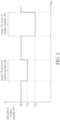
FIG. 2 is a diagram illustrating a RX gain control of the wireless module. -
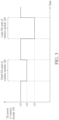
FIG. 3 is a diagram illustrating a TX power control of the wireless module. - Certain terms are used throughout the following description and claims to refer to particular system components. As one skilled in the art will appreciate, manufacturers may refer to a component by different names. This document does not intend to distinguish between components that differ in name but not function. In the following discussion and in the claims, the terms "including" and "comprising" are used in an open-ended fashion, and thus should be interpreted to mean "including, but not limited to ...". The terms "couple" and "couples" are intended to mean either an indirect or a direct electrical connection. Thus, if a first device couples to a second device, that connection may be through a direct electrical connection, or through an indirect electrical connection via other devices and connections.
-
FIG. 1 is a diagram illustrating awireless device 100. As shown inFIG. 1 , thewireless device 100 comprises twowireless modules processor 130, where thewireless module 110 comprises a receiver 112, atransmitter 114 and acontrol circuit 116, and thewireless module 120 comprises areceiver 122, a transmitter 124 and acontrol circuit 126. In this embodiment, thewireless device 100 can be any electronic device capable of wirelessly communicating with one or more electronic devices such as theelectronic device 102, and thewireless modules control circuits control circuits - In the
wireless module 110, the receiver 112 comprises at least one amplifier for amplifying a receiving signal V1 to generate an amplified receiving signal V1', and the amplified receiving signal V1' is transmitted to theprocessor 130 after being processed by other elements, wherein the gain of the receiver 112 (i.e. the gain of at least one amplifier within the receiver 112) is controlled by thecontrol circuit 116. In addition, thetransmitter 114 comprises at least one amplifier for amplifying a transmitting signal V2 from theprocessor 130 to generate an amplified transmitting signal V2', and the amplified transmitting signal V2' is broadcasted via an antenna of thewireless device 100, wherein the gain of the transmitter 114 (i.e. the gain of at least one amplifier within the transmitter 114) is controlled by thecontrol circuit 116. Similarly, in thewireless module 120, thereceiver 122 comprises at least one amplifier for amplifying a receiving signal V3 to generate an amplified receiving signal V3', and the amplified receiving signal V3' is transmitted to theprocessor 130 after being processed by other elements, wherein the gain of the receiver 122 (i.e. the gain of at least one amplifier within the receiver 122) is controlled by thecontrol circuit 126. In addition, the transmitter 124 comprises at least one amplifier for amplifying a transmitting signal V4 from theprocessor 130 to generate an amplified transmitting signal V4', and the amplified transmitting signal V4' is broadcasted via an antenna of thewireless device 100, wherein the gain of the transmitter 124 (i.e. the gain of at least one amplifier within the transmitter 124) is controlled by thecontrol circuit 126. Hereinafter, "TX power" of thewireless module 110/120 is used to indicate the power of the amplified transmitting signal V2'/V4', or the gain of thetransmitter 114/124, or the gain of one or more amplifiers within thetransmitter 114/124, or any other value capable of representing the strength/power/amplitude of the amplified transmitting signal V2'/V4'; and "RX gain" of thewireless module 110/120 is used to indicate the gain of the receiver 112/122, or the gain of one or more amplifiers within the receiver 112/122, or any other amplifying factor contributed by the receiver 112/122. - In
FIG. 1 , thewireless module 110 obtains the transmitter time information provided by thewireless module 120 in a real-time manner, wherein the transmitter time information of thewireless module 120 indicates that when the transmitter 124 of thewireless module 120 transmits the amplified transmitting signal V4'. After receiving the transmitter time information of thewireless module 120, thecontrol circuit 116 refers to the transmitter time information of thewireless module 120 to determine an upper limit of the RX gain of thewireless module 110, so that thecontrol circuit 116 generates the control signal Vc1 to control the RX gain of the wireless module 110 (i.e. the RX gain can be any suitable value lower than the upper limit). Specifically, thecontrol circuit 116 can align the timing of the amplified transmitting signal V4' to determine the upper limit of the RX gain of thewireless module 110, that is thecontrol circuit 116 can lower the upper limit of the RX gain when the transmitter 124 transmits the amplified transmitting signal V4' to mitigate the performance degradation, and thecontrol circuit 116 does not limit the RX gain of thewireless module 110 or uses a predetermined upper limit of the RX gain when the transmitter 124 does not transmit the amplified transmitting signal V4' to maintain the sensitivity. Preferably, the upper limit of the RX gain of thewireless device 110 is determined lower if thewireless device 120 has higher TX power. TakingFIG. 2 as an example, if thewireless module 120 does not transmit any signal, the upper limit of the RX gain of thewireless module 110 is set to be a predetermined upper limit G0 or thecontrol circuit 116 does not set the upper limit (e.g. the upper limit is released when it is detected that thewireless module 120 stops transmitting the transmitting signal); if the TX power of thewireless module 120 is small, thecontrol circuit 116 determines the upper limit G1 of the RX gain of thewireless module 110; and if the TX power of thewireless module 120 is large, thecontrol circuit 116 determines the lower upper limit G2 of the RX gain of thewireless module 110. - Preferably, the
wireless module 110 obtains receiver time information provided by thewireless module 120 in a real-time manner, wherein the receiver time information of thewireless module 120 indicates that when thereceiver 122 of thewireless module 120 receives and processes the receiving signal V3. After receiving the receiver time information of thewireless module 120, thecontrol circuit 116 refers to the receiver time information of thewireless module 120 to determine an upper limit of the TX power of thewireless module 110, so that thecontrol circuit 116 generates the control signal Vc2 to control the TX power of the wireless module 110 (i.e. the TX power can be any suitable value lower than the upper limit). Specifically, thecontrol circuit 116 can align the timing of the receiving signal V3 to determine the upper limit of the TX power of the wireless module 1 10, that is thecontrol circuit 116 can lower the upper limit of the TX power when thereceiver 122 receives and processes the receiving signal V3 to mitigate the performance degradation of thewireless module 120, and thecontrol circuit 116 does not limit the TX power of thewireless module 120 or uses a predetermined upper limit of the TX power when thereceiver 122 does not receive and process the receiving signal V3 to maintain the sensitivity of thewireless module 120. Preferably, the upper limit of the TX power of thewireless device 110 is determined lower if thewireless device 120 has higher RX gain. TakingFIG. 3 as an example, if thewireless module 120 does not receive and process any signal, the upper limit of the TX power of thewireless module 110 is set to be a predetermined upper limit G3 or thecontrol circuit 126 does not set the upper limit; if the RX gain of thewireless module 120 is small, thecontrol circuit 126 determines the upper limit G4 of the TX power of thewireless module 110; and if the RX gain of thewireless module 120 is large, thecontrol circuit 126 determines the lower upper limit G5 of the TX power of thewireless module 110. - Regarding the
wireless module 120, preferably, thewireless module 120 obtains the transmitter time information provided by thewireless module 110 in a real-time manner, wherein the transmitter time information of thewireless module 110 indicates that when thetransmitter 114 of thewireless module 110 transmits the amplified transmitting signal V2'. After receiving the transmitter time information of thewireless module 110, thecontrol circuit 126 refers to the transmitter time information of thewireless module 110 to determine an upper limit of the RX gain of thewireless module 120, so that thecontrol circuit 126 generates the control signal Vc3 to control the RX gain of the wireless module 120 (i.e. the RX gain can be any suitable value lower than the upper limit). Specifically, thecontrol circuit 126 can align the timing of the amplified transmitting signal V2' to determine the upper limit of the RX gain of thewireless module 120, that is thecontrol circuit 126 can lower the upper limit of the RX gain when thetransmitter 114 transmits the amplified transmitting signal V2' to mitigate the performance degradation, and thecontrol circuit 126 does not limit the RX gain of thewireless module 120 or uses a predetermined upper limit of the RX gain when thetransmitter 114 does not transmit the amplified transmitting signal V2' to maintain the sensitivity. Preferably, the upper limit of the RX gain of thewireless device 120 is determined lower if thewireless device 110 has higher TX power, which is similar to the embodiment shown inFIG. 2 . - Preferably, the
wireless module 120 obtains receiver time information provided by thewireless module 110 in a real-time manner, wherein the receiver time information of thewireless module 110 indicates that when the receiver 112 of thewireless module 110 receives and processes the receiving signal V1. After receiving the receiver time information of thewireless module 110, thecontrol circuit 126 refers to the receiver time information of thewireless module 110 to determine an upper limit of the TX power of thewireless module 120, so that thecontrol circuit 126 generates the control signal Vc4 to control the TX power of the wireless module 120 (i.e. the TX power can be any suitable value lower than the upper limit). Specifically, thecontrol circuit 126 can align the timing of the receiving signal V1 to determine the upper limit of the TX power of thewireless module 120, that is thecontrol circuit 126 can lower the upper limit of the TX power when the receiver 112 receives and processes the receiving signal V1 to mitigate the performance degradation of thewireless module 120, and thecontrol circuit 126 does not limit the TX power of thewireless module 120 or uses a predetermined upper limit of the TX power when the receiver 112 does not receive and process the receiving signal V1 to maintain the sensitivity of thewireless module 110. Preferably, the upper limit of the TX power of thewireless device 120 is determined lower if thewireless device 110 has higher RX gain, which is similar to the embodiment shown inFIG. 3 . - By synchronizing the transmitter time information and the receiver time information to each other in a real time manner (i.e. per-packet control), the
wireless module 110 and/or thewireless module 120 can determine the appropriate upper limit of the RX gain and/or the upper limit TX power at the appropriate time, to balance the efficiency of the receiver 112/122 and thetransmitter 114/124. - Those skilled in the art will readily observe that numerous modifications and alterations of the device and method may be made while retaining the teachings of the invention. The intended limitations are defined by the appended claims.
Claims (6)
- A control method of a wireless device, wherein the wireless device (100) comprises a first wireless module (110) and a second wireless module (120), the first wireless module (110) is one of a Wi-Fi module and a Bluetooth module, and the second wireless module (120) is the other one of the Wi-Fi module and the Bluetooth module, and the control method comprises:obtaining first receiver time information that a receiver (112) of the first wireless module (110) receives and processes a receiving signal (V1);characterized by:referring to the first receiver time information to determine an upper limit of a power of a transmitting signal (V4) transmitted by a transmitter (124) of the second wireless module (120);obtaining second receiver time information that a receiver (122) of the second wireless module (120) receives and processes a receiving signal (V3); andreferring to the second receiver time information to determine an upper limit of a power of a transmitting signal (V2) transmitted by a transmitter (114) of the first wireless module (110).
- The control method of claim 1, wherein the step of referring to the first receiver time information to determine the upper limit of the power of the transmitting signal (V4) transmitted by the transmitter (124) of the second wireless module (120) comprises:referring to the first receiver time information to lower the upper limit of the power of the transmitting signal (V4) transmitted by the transmitter (124) of the second wireless module (120) only when the receiver (112) of the first wireless module (110) receives the receiving signal (V1); andwhen the receiver of the first wireless module does not receive any receiving signal (V1), not lowering the upper limit of the power of the transmitting signal (V4) transmitted by transmitter (124) of the second wireless module (120), or using a predetermined upper limit of the power of the transmitting signal (V4).
- The control method of claim 1 or 2, further comprising:obtaining a gain of the receiver (112) of the first wireless module (110); andthe step of referring to the first receiver time information to determine the upper limit of the power of the transmitting signal (V4) transmitted by the transmitter (124) of the second wireless module (120) comprises:
referring to the first receiver time information and the gain of the receiver (112) of the first wireless module (110) to determine the upper limit of the power of the transmitting signal (V4). - The control method of claim 3, wherein the step of referring to the first receiver time
information and the gain of the receiver (112) of the first wireless module (110) to determine the upper limit of the power of the transmitting signal (V4) comprises:when the gain of the receiver (112) of the first wireless module (110) corresponds to a first value, determining a first upper limit of the power of the transmitting signal (V4); andwhen the gain of the receiver (112) of the first wireless module (110) corresponds to a second value greater than the first value, determining a second upper limit of the power of the transmitting signal (V4). - The control method of claim 3 or 4, wherein the gain of the receiver (112) of the first wireless module (110) is obtained in a real-time manner for determining the upper limit of the power of the transmitting signal (V4).
- The control method of any one of claims 1 to 5, further comprisingobtaining transmitter time information that a transmitter (114) of the first wireless module (110) transmits a transmitting signal (V2); andreferring to the transmitter time information to determine an upper limit of a gain of a receiver (122) of the second wireless module (120).
Applications Claiming Priority (2)
| Application Number | Priority Date | Filing Date | Title |
|---|---|---|---|
| US201962823057P | 2019-03-25 | 2019-03-25 | |
| US16/727,942 US11165450B2 (en) | 2019-03-25 | 2019-12-27 | Control method and wireless module applied to wireless device |
Publications (2)
| Publication Number | Publication Date |
|---|---|
| EP3716700A1 EP3716700A1 (en) | 2020-09-30 |
| EP3716700B1 true EP3716700B1 (en) | 2023-10-18 |
Family
ID=69784159
Family Applications (1)
| Application Number | Title | Priority Date | Filing Date |
|---|---|---|---|
| EP20161791.7A Active EP3716700B1 (en) | 2019-03-25 | 2020-03-09 | Control method and wireless module applied to wireless device |
Country Status (4)
| Country | Link |
|---|---|
| US (1) | US11165450B2 (en) |
| EP (1) | EP3716700B1 (en) |
| CN (1) | CN111817740B (en) |
| TW (1) | TWI729745B (en) |
Citations (2)
| Publication number | Priority date | Publication date | Assignee | Title |
|---|---|---|---|---|
| US8781519B2 (en) * | 2012-09-26 | 2014-07-15 | Apple Inc. | Transmission power modulation to facilitate in-device coexistence between wireless communication technologies |
| US20160336984A1 (en) * | 2015-05-12 | 2016-11-17 | Broadcom Corporation | Coexistence signaling for adaptive gain table selection |
Family Cites Families (14)
| Publication number | Priority date | Publication date | Assignee | Title |
|---|---|---|---|---|
| US8026845B2 (en) | 2007-04-16 | 2011-09-27 | Qualcomm Incorporated | Positioning and transmitting system |
| US8023886B2 (en) * | 2007-09-28 | 2011-09-20 | Broadcom Corporation | Method and system for repeater with gain control and isolation via polarization |
| KR101201202B1 (en) | 2008-12-11 | 2012-11-15 | 한국전자통신연구원 | Apparatus for transmitting/receiving rf signal in a wireless communication system |
| US8750926B2 (en) | 2010-06-18 | 2014-06-10 | Mediatek Inc. | System and method for coordinating multiple radio transceivers within the same device platform |
| US8571595B2 (en) * | 2011-04-07 | 2013-10-29 | Blackberry Limited | Method and system for adjusting WLAN radio receiver gain in a wireless device |
| US9297697B2 (en) * | 2012-06-05 | 2016-03-29 | Apple Inc. | In-device coexistence between radios |
| US9723620B2 (en) * | 2012-06-20 | 2017-08-01 | Qualcomm Technologies International, Ltd. | Power-aware coexistence |
| CN103037493B (en) | 2012-12-14 | 2016-08-03 | 中兴通讯股份有限公司 | Dynamically adjust and launch the method and device of power, intelligent terminal |
| US9844057B2 (en) * | 2013-10-21 | 2017-12-12 | Qualcomm Incorporated | Channel usage beacon signal design for cooperative communication systems |
| US9801126B2 (en) * | 2014-10-28 | 2017-10-24 | Alcatel Lucent | Configurable communication modules for flexible communications within an energy-limited wireless system |
| US10098038B2 (en) | 2016-05-31 | 2018-10-09 | Mediatek Inc. | Wireless module and method of reducing interference between multiple wireless antennas |
| CN108322237B (en) | 2017-01-14 | 2020-09-29 | 鸿富锦精密工业(深圳)有限公司 | Interference suppression system and method |
| US10098136B1 (en) | 2017-06-29 | 2018-10-09 | Amazon Technologies, Inc. | Transmit power and receive gain adjustments in multi-radio devices |
| US10135550B1 (en) * | 2017-11-07 | 2018-11-20 | Peraso Technologies Inc. | Wireless transmitter calibration |
-
2019
- 2019-12-27 US US16/727,942 patent/US11165450B2/en active Active
-
2020
- 2020-03-09 EP EP20161791.7A patent/EP3716700B1/en active Active
- 2020-03-24 CN CN202010215078.0A patent/CN111817740B/en active Active
- 2020-03-25 TW TW109109891A patent/TWI729745B/en active
Patent Citations (2)
| Publication number | Priority date | Publication date | Assignee | Title |
|---|---|---|---|---|
| US8781519B2 (en) * | 2012-09-26 | 2014-07-15 | Apple Inc. | Transmission power modulation to facilitate in-device coexistence between wireless communication technologies |
| US20160336984A1 (en) * | 2015-05-12 | 2016-11-17 | Broadcom Corporation | Coexistence signaling for adaptive gain table selection |
Also Published As
| Publication number | Publication date |
|---|---|
| EP3716700A1 (en) | 2020-09-30 |
| CN111817740A (en) | 2020-10-23 |
| TW202037094A (en) | 2020-10-01 |
| US11165450B2 (en) | 2021-11-02 |
| US20200313702A1 (en) | 2020-10-01 |
| TWI729745B (en) | 2021-06-01 |
| CN111817740B (en) | 2022-10-14 |
Similar Documents
| Publication | Publication Date | Title |
|---|---|---|
| CN111327344B (en) | Radio frequency system and electronic equipment | |
| US8260234B2 (en) | Apparatus and method for calibration in multi-antenna system | |
| US20130044695A1 (en) | Fast link establishment for wireless stations operating in millimeter-wave band | |
| US9871641B2 (en) | Apparatus and method for selecting an antenna for uplink communication | |
| CN103843257A (en) | Front-end circuit, impedance adjustment method | |
| US10615839B2 (en) | High-frequency-signal transceiver circuit | |
| US10880021B2 (en) | Wireless communication device and operation method of the same | |
| CN112956140A (en) | Radio frequency communication system with coexistence management based on digital observation data | |
| EP2496027A1 (en) | Method, control equipment and communication system for dynamically adjusting transmission power | |
| EP3485575B1 (en) | Activating interference signal rejection filter path based on detection of an interference signal in a wireless distribution system (wds) | |
| CN101834626B (en) | Mobile terminal, base station and communication system | |
| US20240244540A1 (en) | Transmission power determination for forwarding nodes in wireless communication systems | |
| US20160164496A1 (en) | Methods and systems for dynamically adjusting frequency offsets for mitigating interference | |
| CN110504984A (en) | A kind of electronic equipment | |
| US20180212642A1 (en) | Mobile terminal and system with multichannel transceiver | |
| US10091742B2 (en) | Wireless communication device | |
| US8107890B2 (en) | Multiple frequency band multiple standard device with reduced blocker | |
| US12562774B2 (en) | Radio frequency circuit, communication device, and control method | |
| US20160119016A1 (en) | Antenna switching in a communication circuit | |
| EP3716700A1 (en) | Control method and wireless module applied to wireless device | |
| US10594341B2 (en) | High-frequency-signal transceiver circuit | |
| WO2016185871A1 (en) | Wireless communication device | |
| EP2913936A1 (en) | Integrated receiving apparatus | |
| US20250112666A1 (en) | Radio frequency circuit | |
| CN103762997A (en) | Anti-jamming circuit and radio frequency processing circuit |
Legal Events
| Date | Code | Title | Description |
|---|---|---|---|
| PUAI | Public reference made under article 153(3) epc to a published international application that has entered the european phase |
Free format text: ORIGINAL CODE: 0009012 |
|
| STAA | Information on the status of an ep patent application or granted ep patent |
Free format text: STATUS: THE APPLICATION HAS BEEN PUBLISHED |
|
| AK | Designated contracting states |
Kind code of ref document: A1 Designated state(s): AL AT BE BG CH CY CZ DE DK EE ES FI FR GB GR HR HU IE IS IT LI LT LU LV MC MK MT NL NO PL PT RO RS SE SI SK SM TR |
|
| AX | Request for extension of the european patent |
Extension state: BA ME |
|
| STAA | Information on the status of an ep patent application or granted ep patent |
Free format text: STATUS: REQUEST FOR EXAMINATION WAS MADE |
|
| STAA | Information on the status of an ep patent application or granted ep patent |
Free format text: STATUS: EXAMINATION IS IN PROGRESS |
|
| 17P | Request for examination filed |
Effective date: 20210323 |
|
| RBV | Designated contracting states (corrected) |
Designated state(s): AL AT BE BG CH CY CZ DE DK EE ES FI FR GB GR HR HU IE IS IT LI LT LU LV MC MK MT NL NO PL PT RO RS SE SI SK SM TR |
|
| 17Q | First examination report despatched |
Effective date: 20210413 |
|
| GRAP | Despatch of communication of intention to grant a patent |
Free format text: ORIGINAL CODE: EPIDOSNIGR1 |
|
| RIN1 | Information on inventor provided before grant (corrected) |
Inventor name: HUANG, CHE-WEI Inventor name: HSU, CHANG-YI Inventor name: HSIA, EN-CHIEH Inventor name: HUANG, PO-HSUN Inventor name: SUN, JUEI-TING Inventor name: WEN, YU-MING |
|
| STAA | Information on the status of an ep patent application or granted ep patent |
Free format text: STATUS: GRANT OF PATENT IS INTENDED |
|
| INTG | Intention to grant announced |
Effective date: 20230511 |
|
| P01 | Opt-out of the competence of the unified patent court (upc) registered |
Effective date: 20230607 |
|
| GRAS | Grant fee paid |
Free format text: ORIGINAL CODE: EPIDOSNIGR3 |
|
| GRAA | (expected) grant |
Free format text: ORIGINAL CODE: 0009210 |
|
| STAA | Information on the status of an ep patent application or granted ep patent |
Free format text: STATUS: THE PATENT HAS BEEN GRANTED |
|
| AK | Designated contracting states |
Kind code of ref document: B1 Designated state(s): AL AT BE BG CH CY CZ DE DK EE ES FI FR GB GR HR HU IE IS IT LI LT LU LV MC MK MT NL NO PL PT RO RS SE SI SK SM TR |
|
| REG | Reference to a national code |
Ref country code: GB Ref legal event code: FG4D |
|
| REG | Reference to a national code |
Ref country code: CH Ref legal event code: EP |
|
| REG | Reference to a national code |
Ref country code: IE Ref legal event code: FG4D |
|
| REG | Reference to a national code |
Ref country code: DE Ref legal event code: R096 Ref document number: 602020019306 Country of ref document: DE |
|
| REG | Reference to a national code |
Ref country code: LT Ref legal event code: MG9D |
|
| REG | Reference to a national code |
Ref country code: NL Ref legal event code: MP Effective date: 20231018 |
|
| REG | Reference to a national code |
Ref country code: AT Ref legal event code: MK05 Ref document number: 1623599 Country of ref document: AT Kind code of ref document: T Effective date: 20231018 |
|
| PG25 | Lapsed in a contracting state [announced via postgrant information from national office to epo] |
Ref country code: NL Free format text: LAPSE BECAUSE OF FAILURE TO SUBMIT A TRANSLATION OF THE DESCRIPTION OR TO PAY THE FEE WITHIN THE PRESCRIBED TIME-LIMIT Effective date: 20231018 |
|
| PG25 | Lapsed in a contracting state [announced via postgrant information from national office to epo] |
Ref country code: GR Free format text: LAPSE BECAUSE OF FAILURE TO SUBMIT A TRANSLATION OF THE DESCRIPTION OR TO PAY THE FEE WITHIN THE PRESCRIBED TIME-LIMIT Effective date: 20240119 |
|
| PG25 | Lapsed in a contracting state [announced via postgrant information from national office to epo] |
Ref country code: IS Free format text: LAPSE BECAUSE OF FAILURE TO SUBMIT A TRANSLATION OF THE DESCRIPTION OR TO PAY THE FEE WITHIN THE PRESCRIBED TIME-LIMIT Effective date: 20240218 |
|
| PG25 | Lapsed in a contracting state [announced via postgrant information from national office to epo] |
Ref country code: LT Free format text: LAPSE BECAUSE OF FAILURE TO SUBMIT A TRANSLATION OF THE DESCRIPTION OR TO PAY THE FEE WITHIN THE PRESCRIBED TIME-LIMIT Effective date: 20231018 |
|
| PG25 | Lapsed in a contracting state [announced via postgrant information from national office to epo] |
Ref country code: AT Free format text: LAPSE BECAUSE OF FAILURE TO SUBMIT A TRANSLATION OF THE DESCRIPTION OR TO PAY THE FEE WITHIN THE PRESCRIBED TIME-LIMIT Effective date: 20231018 |
|
| PG25 | Lapsed in a contracting state [announced via postgrant information from national office to epo] |
Ref country code: ES Free format text: LAPSE BECAUSE OF FAILURE TO SUBMIT A TRANSLATION OF THE DESCRIPTION OR TO PAY THE FEE WITHIN THE PRESCRIBED TIME-LIMIT Effective date: 20231018 |
|
| PG25 | Lapsed in a contracting state [announced via postgrant information from national office to epo] |
Ref country code: LT Free format text: LAPSE BECAUSE OF FAILURE TO SUBMIT A TRANSLATION OF THE DESCRIPTION OR TO PAY THE FEE WITHIN THE PRESCRIBED TIME-LIMIT Effective date: 20231018 Ref country code: IS Free format text: LAPSE BECAUSE OF FAILURE TO SUBMIT A TRANSLATION OF THE DESCRIPTION OR TO PAY THE FEE WITHIN THE PRESCRIBED TIME-LIMIT Effective date: 20240218 Ref country code: GR Free format text: LAPSE BECAUSE OF FAILURE TO SUBMIT A TRANSLATION OF THE DESCRIPTION OR TO PAY THE FEE WITHIN THE PRESCRIBED TIME-LIMIT Effective date: 20240119 Ref country code: ES Free format text: LAPSE BECAUSE OF FAILURE TO SUBMIT A TRANSLATION OF THE DESCRIPTION OR TO PAY THE FEE WITHIN THE PRESCRIBED TIME-LIMIT Effective date: 20231018 Ref country code: BG Free format text: LAPSE BECAUSE OF FAILURE TO SUBMIT A TRANSLATION OF THE DESCRIPTION OR TO PAY THE FEE WITHIN THE PRESCRIBED TIME-LIMIT Effective date: 20240118 Ref country code: AT Free format text: LAPSE BECAUSE OF FAILURE TO SUBMIT A TRANSLATION OF THE DESCRIPTION OR TO PAY THE FEE WITHIN THE PRESCRIBED TIME-LIMIT Effective date: 20231018 Ref country code: PT Free format text: LAPSE BECAUSE OF FAILURE TO SUBMIT A TRANSLATION OF THE DESCRIPTION OR TO PAY THE FEE WITHIN THE PRESCRIBED TIME-LIMIT Effective date: 20240219 |
|
| PG25 | Lapsed in a contracting state [announced via postgrant information from national office to epo] |
Ref country code: SE Free format text: LAPSE BECAUSE OF FAILURE TO SUBMIT A TRANSLATION OF THE DESCRIPTION OR TO PAY THE FEE WITHIN THE PRESCRIBED TIME-LIMIT Effective date: 20231018 Ref country code: RS Free format text: LAPSE BECAUSE OF FAILURE TO SUBMIT A TRANSLATION OF THE DESCRIPTION OR TO PAY THE FEE WITHIN THE PRESCRIBED TIME-LIMIT Effective date: 20231018 Ref country code: PL Free format text: LAPSE BECAUSE OF FAILURE TO SUBMIT A TRANSLATION OF THE DESCRIPTION OR TO PAY THE FEE WITHIN THE PRESCRIBED TIME-LIMIT Effective date: 20231018 Ref country code: NO Free format text: LAPSE BECAUSE OF FAILURE TO SUBMIT A TRANSLATION OF THE DESCRIPTION OR TO PAY THE FEE WITHIN THE PRESCRIBED TIME-LIMIT Effective date: 20240118 Ref country code: LV Free format text: LAPSE BECAUSE OF FAILURE TO SUBMIT A TRANSLATION OF THE DESCRIPTION OR TO PAY THE FEE WITHIN THE PRESCRIBED TIME-LIMIT Effective date: 20231018 Ref country code: HR Free format text: LAPSE BECAUSE OF FAILURE TO SUBMIT A TRANSLATION OF THE DESCRIPTION OR TO PAY THE FEE WITHIN THE PRESCRIBED TIME-LIMIT Effective date: 20231018 |
|
| PG25 | Lapsed in a contracting state [announced via postgrant information from national office to epo] |
Ref country code: DK Free format text: LAPSE BECAUSE OF FAILURE TO SUBMIT A TRANSLATION OF THE DESCRIPTION OR TO PAY THE FEE WITHIN THE PRESCRIBED TIME-LIMIT Effective date: 20231018 |
|
| REG | Reference to a national code |
Ref country code: DE Ref legal event code: R097 Ref document number: 602020019306 Country of ref document: DE |
|
| PG25 | Lapsed in a contracting state [announced via postgrant information from national office to epo] |
Ref country code: CZ Free format text: LAPSE BECAUSE OF FAILURE TO SUBMIT A TRANSLATION OF THE DESCRIPTION OR TO PAY THE FEE WITHIN THE PRESCRIBED TIME-LIMIT Effective date: 20231018 |
|
| PG25 | Lapsed in a contracting state [announced via postgrant information from national office to epo] |
Ref country code: SK Free format text: LAPSE BECAUSE OF FAILURE TO SUBMIT A TRANSLATION OF THE DESCRIPTION OR TO PAY THE FEE WITHIN THE PRESCRIBED TIME-LIMIT Effective date: 20231018 |
|
| PG25 | Lapsed in a contracting state [announced via postgrant information from national office to epo] |
Ref country code: SM Free format text: LAPSE BECAUSE OF FAILURE TO SUBMIT A TRANSLATION OF THE DESCRIPTION OR TO PAY THE FEE WITHIN THE PRESCRIBED TIME-LIMIT Effective date: 20231018 Ref country code: SK Free format text: LAPSE BECAUSE OF FAILURE TO SUBMIT A TRANSLATION OF THE DESCRIPTION OR TO PAY THE FEE WITHIN THE PRESCRIBED TIME-LIMIT Effective date: 20231018 Ref country code: RO Free format text: LAPSE BECAUSE OF FAILURE TO SUBMIT A TRANSLATION OF THE DESCRIPTION OR TO PAY THE FEE WITHIN THE PRESCRIBED TIME-LIMIT Effective date: 20231018 Ref country code: IT Free format text: LAPSE BECAUSE OF FAILURE TO SUBMIT A TRANSLATION OF THE DESCRIPTION OR TO PAY THE FEE WITHIN THE PRESCRIBED TIME-LIMIT Effective date: 20231018 Ref country code: EE Free format text: LAPSE BECAUSE OF FAILURE TO SUBMIT A TRANSLATION OF THE DESCRIPTION OR TO PAY THE FEE WITHIN THE PRESCRIBED TIME-LIMIT Effective date: 20231018 Ref country code: DK Free format text: LAPSE BECAUSE OF FAILURE TO SUBMIT A TRANSLATION OF THE DESCRIPTION OR TO PAY THE FEE WITHIN THE PRESCRIBED TIME-LIMIT Effective date: 20231018 Ref country code: CZ Free format text: LAPSE BECAUSE OF FAILURE TO SUBMIT A TRANSLATION OF THE DESCRIPTION OR TO PAY THE FEE WITHIN THE PRESCRIBED TIME-LIMIT Effective date: 20231018 |
|
| PLBE | No opposition filed within time limit |
Free format text: ORIGINAL CODE: 0009261 |
|
| STAA | Information on the status of an ep patent application or granted ep patent |
Free format text: STATUS: NO OPPOSITION FILED WITHIN TIME LIMIT |
|
| 26N | No opposition filed |
Effective date: 20240719 |
|
| PG25 | Lapsed in a contracting state [announced via postgrant information from national office to epo] |
Ref country code: SI Free format text: LAPSE BECAUSE OF FAILURE TO SUBMIT A TRANSLATION OF THE DESCRIPTION OR TO PAY THE FEE WITHIN THE PRESCRIBED TIME-LIMIT Effective date: 20231018 |
|
| PG25 | Lapsed in a contracting state [announced via postgrant information from national office to epo] |
Ref country code: SI Free format text: LAPSE BECAUSE OF FAILURE TO SUBMIT A TRANSLATION OF THE DESCRIPTION OR TO PAY THE FEE WITHIN THE PRESCRIBED TIME-LIMIT Effective date: 20231018 |
|
| REG | Reference to a national code |
Ref country code: CH Ref legal event code: PL |
|
| PG25 | Lapsed in a contracting state [announced via postgrant information from national office to epo] |
Ref country code: LU Free format text: LAPSE BECAUSE OF NON-PAYMENT OF DUE FEES Effective date: 20240309 |
|
| PG25 | Lapsed in a contracting state [announced via postgrant information from national office to epo] |
Ref country code: MC Free format text: LAPSE BECAUSE OF FAILURE TO SUBMIT A TRANSLATION OF THE DESCRIPTION OR TO PAY THE FEE WITHIN THE PRESCRIBED TIME-LIMIT Effective date: 20231018 |
|
| PG25 | Lapsed in a contracting state [announced via postgrant information from national office to epo] |
Ref country code: MC Free format text: LAPSE BECAUSE OF FAILURE TO SUBMIT A TRANSLATION OF THE DESCRIPTION OR TO PAY THE FEE WITHIN THE PRESCRIBED TIME-LIMIT Effective date: 20231018 Ref country code: LU Free format text: LAPSE BECAUSE OF NON-PAYMENT OF DUE FEES Effective date: 20240309 |
|
| REG | Reference to a national code |
Ref country code: BE Ref legal event code: MM Effective date: 20240331 |
|
| PG25 | Lapsed in a contracting state [announced via postgrant information from national office to epo] |
Ref country code: BE Free format text: LAPSE BECAUSE OF NON-PAYMENT OF DUE FEES Effective date: 20240331 |
|
| PG25 | Lapsed in a contracting state [announced via postgrant information from national office to epo] |
Ref country code: IE Free format text: LAPSE BECAUSE OF NON-PAYMENT OF DUE FEES Effective date: 20240309 |
|
| PG25 | Lapsed in a contracting state [announced via postgrant information from national office to epo] |
Ref country code: IE Free format text: LAPSE BECAUSE OF NON-PAYMENT OF DUE FEES Effective date: 20240309 Ref country code: BE Free format text: LAPSE BECAUSE OF NON-PAYMENT OF DUE FEES Effective date: 20240331 Ref country code: CH Free format text: LAPSE BECAUSE OF NON-PAYMENT OF DUE FEES Effective date: 20240331 |
|
| PG25 | Lapsed in a contracting state [announced via postgrant information from national office to epo] |
Ref country code: CY Free format text: LAPSE BECAUSE OF FAILURE TO SUBMIT A TRANSLATION OF THE DESCRIPTION OR TO PAY THE FEE WITHIN THE PRESCRIBED TIME-LIMIT; INVALID AB INITIO Effective date: 20200309 |
|
| PG25 | Lapsed in a contracting state [announced via postgrant information from national office to epo] |
Ref country code: HU Free format text: LAPSE BECAUSE OF FAILURE TO SUBMIT A TRANSLATION OF THE DESCRIPTION OR TO PAY THE FEE WITHIN THE PRESCRIBED TIME-LIMIT; INVALID AB INITIO Effective date: 20200309 |
|
| PG25 | Lapsed in a contracting state [announced via postgrant information from national office to epo] |
Ref country code: FI Free format text: LAPSE BECAUSE OF FAILURE TO SUBMIT A TRANSLATION OF THE DESCRIPTION OR TO PAY THE FEE WITHIN THE PRESCRIBED TIME-LIMIT Effective date: 20231019 |
|
| PG25 | Lapsed in a contracting state [announced via postgrant information from national office to epo] |
Ref country code: TR Free format text: LAPSE BECAUSE OF FAILURE TO SUBMIT A TRANSLATION OF THE DESCRIPTION OR TO PAY THE FEE WITHIN THE PRESCRIBED TIME-LIMIT Effective date: 20231018 |
|
| PGFP | Annual fee paid to national office [announced via postgrant information from national office to epo] |
Ref country code: FR Payment date: 20251231 Year of fee payment: 7 |
|
| PGFP | Annual fee paid to national office [announced via postgrant information from national office to epo] |
Ref country code: GB Payment date: 20260106 Year of fee payment: 7 |
|
| PGFP | Annual fee paid to national office [announced via postgrant information from national office to epo] |
Ref country code: DE Payment date: 20260102 Year of fee payment: 7 |