EP3714496B1 - Overcharge protection device with uneven terminal pads - Google Patents
Overcharge protection device with uneven terminal pads Download PDFInfo
- Publication number
- EP3714496B1 EP3714496B1 EP18815485.0A EP18815485A EP3714496B1 EP 3714496 B1 EP3714496 B1 EP 3714496B1 EP 18815485 A EP18815485 A EP 18815485A EP 3714496 B1 EP3714496 B1 EP 3714496B1
- Authority
- EP
- European Patent Office
- Prior art keywords
- terminal pad
- terminal
- overcharge protection
- cover assembly
- protection device
- Prior art date
- Legal status (The legal status is an assumption and is not a legal conclusion. Google has not performed a legal analysis and makes no representation as to the accuracy of the status listed.)
- Active
Links
Images

Classifications
-
- H—ELECTRICITY
- H01—ELECTRIC ELEMENTS
- H01M—PROCESSES OR MEANS, e.g. BATTERIES, FOR THE DIRECT CONVERSION OF CHEMICAL ENERGY INTO ELECTRICAL ENERGY
- H01M50/00—Constructional details or processes of manufacture of the non-active parts of electrochemical cells other than fuel cells, e.g. hybrid cells
- H01M50/10—Primary casings; Jackets or wrappings
- H01M50/147—Lids or covers
-
- H—ELECTRICITY
- H01—ELECTRIC ELEMENTS
- H01M—PROCESSES OR MEANS, e.g. BATTERIES, FOR THE DIRECT CONVERSION OF CHEMICAL ENERGY INTO ELECTRICAL ENERGY
- H01M50/00—Constructional details or processes of manufacture of the non-active parts of electrochemical cells other than fuel cells, e.g. hybrid cells
- H01M50/50—Current conducting connections for cells or batteries
- H01M50/572—Means for preventing undesired use or discharge
- H01M50/574—Devices or arrangements for the interruption of current
- H01M50/578—Devices or arrangements for the interruption of current in response to pressure
-
- H—ELECTRICITY
- H01—ELECTRIC ELEMENTS
- H01M—PROCESSES OR MEANS, e.g. BATTERIES, FOR THE DIRECT CONVERSION OF CHEMICAL ENERGY INTO ELECTRICAL ENERGY
- H01M10/00—Secondary cells; Manufacture thereof
- H01M10/42—Methods or arrangements for servicing or maintenance of secondary cells or secondary half-cells
- H01M10/44—Methods for charging or discharging
-
- H—ELECTRICITY
- H01—ELECTRIC ELEMENTS
- H01M—PROCESSES OR MEANS, e.g. BATTERIES, FOR THE DIRECT CONVERSION OF CHEMICAL ENERGY INTO ELECTRICAL ENERGY
- H01M50/00—Constructional details or processes of manufacture of the non-active parts of electrochemical cells other than fuel cells, e.g. hybrid cells
- H01M50/10—Primary casings; Jackets or wrappings
- H01M50/172—Arrangements of electric connectors penetrating the casing
-
- H—ELECTRICITY
- H01—ELECTRIC ELEMENTS
- H01M—PROCESSES OR MEANS, e.g. BATTERIES, FOR THE DIRECT CONVERSION OF CHEMICAL ENERGY INTO ELECTRICAL ENERGY
- H01M50/00—Constructional details or processes of manufacture of the non-active parts of electrochemical cells other than fuel cells, e.g. hybrid cells
- H01M50/50—Current conducting connections for cells or batteries
- H01M50/543—Terminals
-
- H—ELECTRICITY
- H01—ELECTRIC ELEMENTS
- H01M—PROCESSES OR MEANS, e.g. BATTERIES, FOR THE DIRECT CONVERSION OF CHEMICAL ENERGY INTO ELECTRICAL ENERGY
- H01M2200/00—Safety devices for primary or secondary batteries
- H01M2200/20—Pressure-sensitive devices
-
- H—ELECTRICITY
- H01—ELECTRIC ELEMENTS
- H01M—PROCESSES OR MEANS, e.g. BATTERIES, FOR THE DIRECT CONVERSION OF CHEMICAL ENERGY INTO ELECTRICAL ENERGY
- H01M50/00—Constructional details or processes of manufacture of the non-active parts of electrochemical cells other than fuel cells, e.g. hybrid cells
- H01M50/50—Current conducting connections for cells or batteries
- H01M50/543—Terminals
- H01M50/547—Terminals characterised by the disposition of the terminals on the cells
- H01M50/55—Terminals characterised by the disposition of the terminals on the cells on the same side of the cell
-
- H—ELECTRICITY
- H01—ELECTRIC ELEMENTS
- H01M—PROCESSES OR MEANS, e.g. BATTERIES, FOR THE DIRECT CONVERSION OF CHEMICAL ENERGY INTO ELECTRICAL ENERGY
- H01M50/00—Constructional details or processes of manufacture of the non-active parts of electrochemical cells other than fuel cells, e.g. hybrid cells
- H01M50/50—Current conducting connections for cells or batteries
- H01M50/543—Terminals
- H01M50/552—Terminals characterised by their shape
- H01M50/553—Terminals adapted for prismatic, pouch or rectangular cells
-
- Y—GENERAL TAGGING OF NEW TECHNOLOGICAL DEVELOPMENTS; GENERAL TAGGING OF CROSS-SECTIONAL TECHNOLOGIES SPANNING OVER SEVERAL SECTIONS OF THE IPC; TECHNICAL SUBJECTS COVERED BY FORMER USPC CROSS-REFERENCE ART COLLECTIONS [XRACs] AND DIGESTS
- Y02—TECHNOLOGIES OR APPLICATIONS FOR MITIGATION OR ADAPTATION AGAINST CLIMATE CHANGE
- Y02E—REDUCTION OF GREENHOUSE GAS [GHG] EMISSIONS, RELATED TO ENERGY GENERATION, TRANSMISSION OR DISTRIBUTION
- Y02E60/00—Enabling technologies; Technologies with a potential or indirect contribution to GHG emissions mitigation
- Y02E60/10—Energy storage using batteries
Definitions
- the present disclosure relates generally to the field of batteries and battery cells. More specifically, the present disclosure relates to features of a battery cell that may protect a battery cell from thermal runaway during an overcharge event.
- This section is intended to introduce the reader to various aspects of art that may be related to various aspects of the present disclosure, which are described below. This discussion is believed to be helpful in providing the reader with background information to facilitate a better understanding of the various aspects of the present disclosure. Accordingly, it should be understood that these statements are to be read in this light, and not as admissions of prior art.
- Li-ion batteries When charging a rechargeable battery cell, the chemical reactions within the battery cell may cause an increase in temperature.
- Some types of battery cells such as those of lithium-ion (Li-ion) batteries, may be susceptible to thermal runaway, in which the temperature increase caused by the charge cycle causes a further increase in temperature. Thermal runaway can compromise or destroy the battery cell, but also cause damage to the charger and the housing and/or device in which the battery cell is located.
- the document EP 2 299 512 A1 relates to a rechargeable battery that includes an electrode assembly including a first electrode, a second electrode, and a separator disposed between the first and second electrodes.
- the battery further includes a case housing the electrode assembly, and a cap assembly connected to the case.
- the cap assembly includes a first short-circuit tab electrically connected to the first electrode, a second short-circuit tab electrically connected to the second electrode, a deformable plate electrically connecting the first short circuit tab to the second short circuit tab by being transformed upon the pressure increase, and a connection member formed between the short-circuit tab and the deformable plate or formed between the short-circuit tab and the electrode assembly.
- the present invention relates to an overcharge protection device cover assembly according to independent claims 1 and 8, wherein further developments of the invention are provided in the sub-claims, respectively.
- the present disclosure relates to an overcharge protection device cover assembly for use with a battery cell housing, the battery cell housing having a first terminal and a second terminal, the overcharge protection device cover assembly comprising: a first terminal pad having a first length, the first terminal pad being contactable with the first terminal of the battery cell housing; a second terminal pad having a second length that is greater than the first length, the second terminal pad being contactable with the second terminal of the battery cell housing; a reversal device that is deflectable toward the first and second terminal pads; and a conductive element between the reversal device and the first and second terminal pads.
- the present disclosure also relates to an overcharge protection device cover assembly, the overcharge protection device cover assembly having a base plate including a reversal device, the reversal device being transitionable between a first configuration and a second configuration; a first terminal pad having a first length; a second terminal pad having a second length that is greater than the first length; a conductive element between the reversal device and the first and second terminal pads; and a spacer plate between the base plate and the first terminal pad.
- the first terminal pad is a first distance from the base plate when the reversal device is in the first configuration and the second terminal pad is a second distance from the base plate when the reversal device is in the first configuration, the first distance being greater than the second distance.
- the present disclosure also relates to a battery cell having a battery cell housing, the battery cell housing including first terminal and a second terminal; and an overcharge protection device cover assembly affixable to the battery cell housing.
- the overcharge protection device cover assembly includes a base plate coupled to the battery cell housing between the first and second terminals, the base plate having a reversal device that is transitionable between a first configuration and a second configuration; a first terminal pad having a first end portion, a second end portion opposite the first end portion, and a first length, the first end portion of the first terminal pad being in contact with the first terminal; a second terminal pad having a first end portion, a second end portion opposite the first end portion, and a second length that is greater than the first length, the first end portion of the second terminal pad being in contact with the second terminal.
- the battery cell also includes a conductive element between the reversal device and the first and second terminal pads; and a spacer plate between the base plate and the first terminal pad, the first terminal pad being a first distance from the base plate when the reversal device is in the first configuration and the second terminal pad being a second distance from the base plate when the reversal device is in the first configuration, the first distance being greater than the second distance.
- an overcharge protection device cover assembly 10 constructed in accordance with the principles of the present disclosure is shown in FIGS. 1-5 .
- the overcharge protection device cover assembly 10 is shown coupled to a battery cell housing 12 in FIG. 1 .
- the overcharge protection device cover assembly 10 and the battery cell housing 12 are collectively referred to herein as a battery cell 14.
- the overcharge protection device cover assembly 10 includes a base plate 16 configured to be in contact with, adjacent, or coupled to the battery cell housing 12, a first (or negative) terminal pad 18 in contact with a first (or negative) terminal 20, a second (or positive) terminal pad 22 in contact with a second (or positive) terminal 24, a reversal device 26 (reversal device 26 is not visible in FIG.
- the conductive element 28 is in the shape of disk, but other shapes can be used depending in design requirements, e.g., rectangle, square, etc.
- the reversal device 26 is shaped in the form of a disk, but other shapes can be implemented depending on design requirements.
- the reversal device is formed of a metal or polymer that allows the inner portion of the deflection device 26 to deflect from a first position to a second position, the second position allowing activation of the overcharging protection by electrically short-circuiting the battery terminals.
- the overcharge protection device cover assembly 10 is configured to be coupled to a surface of the battery cell housing 12 between the first 20 and second 24 terminals.
- the reversal device 26 is integrated with, defined by, or coupled to the base plate 16, and at least a portion of the reversal device 26 is deflectable.
- the reversal device 26 may be composed of a more flexible material or may be thinner than the base plate 16, such that internal pressure within the battery cell housing 12 is able to deflect the reversal device 26 but not the base plate 16.
- the conductive element 28 is movable, at least in a linear direction that is orthogonal to, or at least substantially orthogonal to, the base plate 16.
- the overcharge protection device cover assembly 10 also includes a vent aperture 30 configured to be aligned with a vent (not shown) in the battery cell housing 12 when the overcharge protection device cover assembly 10 is coupled to the battery cell housing 12.
- the overcharge protection device cover assembly 10 also includes an electrolyte aperture 32 to enable the addition of electrolyte to battery cell within the battery cell housing 12.
- the overcharge protection device cover assembly 10 includes asymmetric first 18 and second 22 terminal pads.
- the second terminal pad 22 has a length L SP that is less than a length L FP of the first terminal pad 18 (for example, as shown in FIG. 2 ).
- the first terminal pad 18 may have a length L FP that is less than the length L SP of the second terminal pad 22.
- the first 18 and second 22 terminal pads are in contact with or coupled to the first 20 and second 24 terminals, respectively.
- the first terminal pad 18 includes a first end portion 34 that is in contact with or coupled to the first terminal 20 and a second end portion 36 opposite the first end portion 34.
- the second end portion 36 is not coupled to any other component of the overcharge protection device cover assembly 10, and is freely movable relative to the base plate 16 in a linear direction that is crosswise (e.g., orthogonal) to the base plate 16.
- the first end portion 34 of the first terminal pad 18 includes a pivot point 38 at the first terminal 20 about which the first terminal pad 18 may move.
- the second terminal pad 22 includes a first end portion 40 that is in contact with or coupled to the second terminal 24 and a second end portion 42 opposite the first end portion 40.
- the second end portion 42 is not coupled to any other component of the overcharge protection device cover assembly 10, and is freely movable relative to the base plate 16 in a linear direction that is orthogonal to, or at least substantially orthogonal to, the base plate 16.
- the first end portion 40 of the second terminal pad 22 includes a pivot point 44 at the second terminal 24 about which the second terminal pad 22 may move.
- the overcharge protection device cover assembly 10 is transitionable from a first configuration (for example, as in a normal operating condition, as shown in FIGS. 2 and 4 ) to a second configuration (for example, as in an electrical short circuit condition, as shown in FIGS. 3 and 5 ).
- the second end portions 36, 42 are disclosed herein as being movable in a linear direction relative to the base plate 16, it will be understood that the second end portions 36, 42 will move about their corresponding pivot points in an arc, albeit a small arc.
- the reversal device 26 is deflectable or transitionable between a first (inverted) configuration and a second (everted) configuration, and transition of the reversal device 26 between the first and second configurations causes the overcharge protection device cover assembly 10 as a whole to transition between the first and second configurations.
- the first 18 and second 22 terminal pads are uneven in height, although they each lie in a plane that is parallel to, or at least substantially parallel to, the plane in which the base plate 16 lies.
- the first terminal pad 18 includes a first (or upper) surface 46 and a second (or lower) surface 48 opposite the first surface 46.
- the second terminal pad 22 includes a first (or upper) surface 50 and a second (or lower) surface 52 opposite the first surface 50.
- the overcharge protection device cover assembly 10 also includes a spacer plate 54 between the base plate 16 and the first terminal pad 18, thereby positioning the first terminal pad 18 at a greater distance from the base plate 16, the reversal device 26, and the conductive element 28.
- the spacer plate 54 lies in a plane that is parallel to, or at least substantially parallel to, the base plate 16. The cross-sectional view of FIG. 2 shows that the first terminal pad 18 and the second terminal pad 22 are not coplanar when the overcharge protection device cover assembly 10 is in the normal operating condition.
- each terminal pad 18, 22 has a working thickness T.
- the working thickness T is the thickness of at least the second end portion 36, 54 of each terminal pad 18, 34 proximate the conductive element 28, at the location with which the conductive element 28 comes into contact with each terminal pad 18, 34 when the overcharge protection device cover assembly 10 is in the short condition.
- the working thickness T of each terminal pad 18, 22 is the same.
- the reversal device 26 As the second terminal pad 22 is located closer to the base plate 16, the reversal device 26, and the conductive element 28 (due to the lack of a spacer plate 54 between the base plate 16 and the second terminal pad 22), deflection of the reversal device 26 will cause the conductive element 28 to come into contact with the second surface 52 of the second terminal pad 22 before the second surface 48 of the first terminal pad 18.
- the second terminal pad 22 has a greater length L SP than the length L FP of the first terminal pad 18, the second terminal pad 22 is more easily pivoted at its pivot point 44 and moved linearly until at least a portion of the second end portion 42 of the second terminal pad 22 is at the same distance from the base plate 16 as at least a portion of the second end portion 36 of the first terminal pad 18 (for example, as shown in FIG. 3 ).
- at least a portion of the second surface 48 of the first terminal pad 18 and at least a portion of the second surface 52 of the second terminal pad 22 are aligned, as they are both in contact with the conductive element 28 when the overcharge protection device cover assembly 10 is in the electrical short circuit condition.
- the conductive element 28 In the electrical short circuit condition, the conductive element 28 is in contact with both the first terminal pad 18 and the second terminal pad 22, establishing a short circuit to prevent the battery cell from overcharging.
- the second terminal pad 22 When the conductive element 28 is in contact with both terminal pads 18, 22, the second terminal pad 22 may be pivoted about its pivot point 44, thereby creating an angle between the plane in which the base plate 16 lies and the plane in which the second terminal pad 22 lies. This angle may be very small, such as approximately 10° or less in some embodiments.
- terminal pads 18, 22 are not coplanar when the overcharge protection device cover assembly 10 is in the normal operating condition, and that at least a portion of each of the first surfaces 46, 50 of the terminal pads 18, 22 are aligned when the overcharge protection device cover assembly 10 is in the electrical short circuit condition, the terminal pads 18, 22 may be configured differently that that shown, provided the conductive element 28 contacts one of the terminal pads 18, 22 before the other when the reversal device 26 deflects to move the conductive element 28 toward the terminal pads 18, 22.
- FIGS. 4 and 5 a second embodiment of an overcharge protection device cover assembly 10 is shown.
- the second embodiment of the overcharge protection device cover assembly 10 of FIGS. 4 and 5 is similar to the first embodiment of the overcharge protection device cover assembly 10 of FIGS. 2 and 3 and, therefore, the same references numbers are used.
- the second embodiment of the overcharge protection device cover assembly 10 includes first 18 and second 22 terminal pads with different working thicknesses T FP and T SP at the second end portion 36 of the first terminal pad 18 proximate the conductive element 28 and at the second end portion 42 of the second terminal pad 22 proximate the conductive element 28.
- the second terminal pad 22 has a working thickness T SP that is greater than the working thickness T FP of the first terminal pad 18.
- the first 18 and second 22 terminal pads are uneven in height. That is, the first surface 46 of the first terminal pad 18 and the first surface 50 of the second terminal pad 22 are located at different distances from the base plate 16, the reversal device 26, and the conductive element 28.
- the second surface 48 of the first terminal pad 18 and the second surface 52 of the second terminal pad 22 are also located at different distances from the base plate 16, the reversal device 26, and the conductive element 28.
- the second surface 48 of the first terminal pad 18 is located a first distance D FP from the base plate 16 and the second surface 52 of the second terminal pad 22 is located a second distance D SP from the base plate 16.
- the overcharge protection device cover assembly 10 includes s spacer plate 54 between the base plate 16 and the first terminal pad 18.
- the cross-sectional view of FIG. 5 shows that the first terminal pad 18 and the second terminal pad 22 are not coplanar when the overcharge protection device cover assembly 10 is in the normal operating condition.
- deflection of the reversal device 26 exerts a force against the conductive element 28, moving the conductive element 28 toward and into contact with the second surface 48 of the first terminal pad 18 and the second surface 52 of the second terminal pad 22.
- the second terminal pad 22 is located closer to the base plate 16, the reversal device 26, and the conductive element 28 (due to the lack of a spacer plate 54 between the base plate 16 and the second terminal pad 22), deflection of the reversal device 26 will case the conductive element 28 to come into contact with the second surface 52 of the second terminal pad 22 before the second surface 48 of the first terminal pad 18.
- the second terminal pad 22 has a greater length L SP than the length L FP of the first terminal pad 18, the second terminal pad 22 is more easily pivoted at its pivot point 44 and moved linearly until at least a portion of the second end portion 42 of the second terminal pad 22 is at the same distance from the base plate 16 as at least a portion of the second end portion 36 of the first terminal pad 18 (for example, as shown in FIG. 3 ).
- at least a portion of the second surface 48 of the first terminal pad 18 and at least a portion of the second surface 52 of the second terminal pad 22 are aligned, as they are both in contact with the conductive element 28 when the overcharge protection device cover assembly 10 is in the electrical short circuit condition.
- the conductive element 28 In the electrical short circuit condition, the conductive element 28 is in contact with both the first terminal pad 18 and the second terminal pad 22, establishing a short circuit to prevent the battery cell from overcharging.
- the second terminal pad 22 may be pivoted about its pivot point 44. Further, as the second end portion 36 of the first terminal pad 18 and second end portion 42 of the second terminal pad 22 are aligned when the overcharge protection device cover assembly 10 is in the electrical short circuit condition and reversal device 26 is fully deflected (everted), with the conductive element 28 is at the its furthest distance from the base plate 16, rather than when the overcharge protection device cover assembly 10 is in the normal operating condition, much less precision is required during manufacture and assembly.
- the configuration of the first 18 and second 22 terminal pads ensures the conductive element 28 will reliably contact both terminal pads 18, 22 to establish a short circuit when overcharge protection is needed. It will be understood that although FIG. 2 shows that the terminal pads 18, 22 are not coplanar when the overcharge protection device cover assembly 10 is in the normal operating condition, and that at least a portion of each of the first surfaces 46, 50 of the terminal pads 18, 22 are aligned when the overcharge protection device cover assembly 10 is in the electrical short circuit condition, the terminal pads 18, 22 may be configured differently that that shown, provided the conductive element 28 contacts one of the terminal pads 18, 22 before the other when the reversal device 26 deflects to move the conductive element 28 toward the terminal pads 18, 22.
- an overcharge protection device cover assembly constructed in accordance with the principles of the present disclosure provides certain benefits over currently known overcharge protection devices.
- the overcharge protection device cover assemblies 10 disclosed herein each include terminal pads 18, 22 of unequal heights from the base plate 16 and conductive element 28 when the overcharge protection device cover assembly 10 is in a normal operating condition. This reduces manufacturing cost and complexity, as the terminal pads 18, 22 do not require precise alignment during assembly.
- the terminal pads 18, 22 also are of unequal lengths (that is, the second terminal pads 22 are longer than the first terminal pads 18) to allow the longer terminal pad 22 to pivot more easily on its pivot point 44.
- deflection of the reversal device 26 causes the conductive element 28 to contact the longer second terminal pad 22 before the shorter first terminal pad 18.
- an overcharge protection device cover assembly 10 for use with a battery cell housing 12 having first terminal 20 and a second terminal 24 includes a first terminal pad 18 having a first length L FP , the first terminal pad 18 being contactable with the first terminal 20 of the battery cell housing 12, and a second terminal pad 22 having a second length L SP that is greater than the first length L FP , the second terminal pad 22 being contactable with the second terminal 24 of the battery cell housing 12.
- the overcharge protection device cover assembly 10 also includes a reversal device 26 that is deflectable toward the first 18 and second 22 terminal pads and a conductive element 28 between the reversal device 26 and the first 18 and second 22 terminal pads.
- the first terminal pad 18 includes a first end portion 34 and a second end portion 36 opposite the first end portion 34 and the second terminal pad 22 includes a first end portion 40 and a second end portion 42 opposite the first end portion 40, the first end portion 40 of the first terminal pad 18 being contactable with the first terminal 20 of the battery cell housing 12 and the first end portion 40 of the second terminal pad 22 being contactable with the second terminal 24 of the battery cell housing 12.
- the first terminal pad 18 includes a first pivot point 38 about which the first terminal pad 18 is pivotable and the second terminal pad 22 includes a second pivot point 44 about which the second terminal pad 22 is pivotable.
- the overcharge protection device cover assembly 10 further includes a base plate 16, the base plate 16 defining the reversal device 26, and a spacer plate 54 between the base plate 16 and the first terminal pad 18.
- the second end portion 36 of the first terminal pad 18 and the second end portion 42 of the second terminal pad 22 are each movable in a direction that is orthogonal to a plant of the base plate 16.
- the reversal device 26 is transitionable between a first configuration and a second configuration.
- the first terminal pad 18 is a first distance from the reversal device 26 when the reversal device 26 is in the first configuration and the second terminal pad 22 is a second distance from the reversal device 26 when the reversal device 26 is in the first configuration, the first distance being greater than the second distance.
- each of the first and second terminal pads includes a working thickness T, the working thickness T of the first terminal pad and the working thickness T of the second terminal pad being the same.
- the first terminal pad 18 includes a first working thickness T FP and the second terminal pad 22 includes a second working thickness T SP that is greater than the first working thickness T FP .
- transition of the reversal device 26 from the first configuration to the second configuration causes the conductive element 28 to contact the second terminal pad 22 before the conductive element 28 contacts the first terminal pad 18.
- an overcharge protection device cover assembly 10 includes a base plate 16 including a reversal device 26, the reversal device 26 being transitionable between a first configuration and a second configuration, a first terminal pad 18 having a first length L FP , a second terminal pad 22 having a second length L SP that is greater than the first length L FP , a conductive element 28 between the reversal device 26 and the first 18 and second 22 terminal pads, and a spacer plate 54 between the base plate 16 and the first terminal pad 18.
- the first terminal pad 18 is a first distance from the base plate 16 when the reversal device 26 is in the first configuration and the second terminal pad 22 is a second distance from the base plate 16 when the reversal device 26 is in the first configuration, the first distance being greater than the second distance.
- each of the first and second terminal pads includes a working thickness T, the working thickness T of the first terminal pad and the working thickness T of the second terminal pad being the same.
- the first terminal pad 18 includes a first working thickness T FP and the second terminal pad 22 includes a second working thickness T SP that is greater than the first working thickness T FP .
- transition of the reversal device 26 from the first configuration to the second configuration causes the conductive element 28 to contact the second terminal pad 22 before the conductive element 28 contacts the first terminal pad 18.
- a battery cell 14 includes a battery cell housing 12, the battery cell housing 12 including first terminal 20 and a second terminal 24, and an overcharge protection device cover assembly 10 affixable to the battery cell housing 12.
- the overcharge protection device cover assembly 10 includes: a base plate 16 coupled to the battery cell housing 12 between the first 32 and second 36 terminals, the base plate 16 having a reversal device 26 that is transitionable between a first configuration and a second configuration; a first terminal pad 18 having a first end portion 34, a second end portion 36 opposite the first end portion 34, and a first length L FP , the first end portion 34 of the first terminal pad 18 being in contact with the first terminal 20; a second terminal pad 22 having a first end portion 40, a second end portion 42 opposite the first end portion 40, and a second length L SP that is greater than the second length L FP , the first end portion 40 of the second terminal pad 22 being in contact with the second terminal 24; a conductive element 28 between the reversal device 26 and the first 30 and second 34 terminal
- the first terminal pad 18 is a first distance from the base plate 16 when the reversal device 26 is in the first configuration and the second terminal pad 22 is a second distance from the base plate 16 when the reversal device 26 is in the first configuration, the first distance being greater than the second distance.
- the second end portion of each of the first and second terminal pads includes a working thickness T, the working thickness T of the second end portion of each of the first terminal pad and the working thickness T of the second terminal pad being the same.
- the second end portion of the first terminal pad 18 has a first working thickness T FP and the second end portion of the second terminal pad 22 has a second working thickness T SP that is greater than the first working thickness T FP .
- transition of the reversal device 26 from the first configuration to the second configuration causes the conductive element 28 to contact the second terminal pad 22 before the conductive element 28 contacts the first terminal pad 18.
- the conductive element 28 is in contact with the first 30 and second 34 terminal pads when the conductive element 28 is in the second configuration. In one aspect of the embodiment, a short circuit is established in the battery cell 14 when the conductive element 28 is in the second configuration.
- the disclosed embodiments may provide one or more technical effects useful in the manufacture of battery cells, and portions of battery cells.
- the disclosed embodiments relate to battery cells that include an overcharge protection assembly.
- the overcharge protection assembly may include a reversal device that is activated when a pressure in a casing of the battery cell reaches a threshold value. The activation of the reversal device may cause electrical contact between terminals of the battery cell, which may create an external circuit by electrically coupling the positive terminal and the negative terminal of the battery cell. Such an external short circuit may discharge the battery cell, but the external short circuit may prevent thermal runaway and/or permanent damage to the battery cell.
- the short circuit may cause a large amount of current to be transmitted through an internal current collector of the battery cell, which may cause the current collector to melt and thereby cut the flow of electric current.
Landscapes
- Chemical & Material Sciences (AREA)
- Chemical Kinetics & Catalysis (AREA)
- Electrochemistry (AREA)
- General Chemical & Material Sciences (AREA)
- Engineering & Computer Science (AREA)
- Manufacturing & Machinery (AREA)
- Connection Of Batteries Or Terminals (AREA)
Description
- The present disclosure relates generally to the field of batteries and battery cells. More specifically, the present disclosure relates to features of a battery cell that may protect a battery cell from thermal runaway during an overcharge event. This section is intended to introduce the reader to various aspects of art that may be related to various aspects of the present disclosure, which are described below. This discussion is believed to be helpful in providing the reader with background information to facilitate a better understanding of the various aspects of the present disclosure. Accordingly, it should be understood that these statements are to be read in this light, and not as admissions of prior art.
- When charging a rechargeable battery cell, the chemical reactions within the battery cell may cause an increase in temperature. Some types of battery cells, such as those of lithium-ion (Li-ion) batteries, may be susceptible to thermal runaway, in which the temperature increase caused by the charge cycle causes a further increase in temperature. Thermal runaway can compromise or destroy the battery cell, but also cause damage to the charger and the housing and/or device in which the battery cell is located.
- As technology continues to evolve, there is a need to provide improved power sources, particularly battery cells and battery modules, for such systems that may be powered by or store their energy using battery technologies. For example, certain types of battery modules may undergo overcharge testing to determine boundaries and/or limits of the battery module and its individual battery cells. Additionally, in certain instances, for example due to changing environmental conditions or other operating conditions, battery cells may be subject to overcharging. Overcharge tests and overcharging may lead to thermal runaway. Therefore, it is recognized that a need exists for devices that may prevent or block thermal runaway.
- The document
EP 2 299 512 A1 relates to a rechargeable battery that includes an electrode assembly including a first electrode, a second electrode, and a separator disposed between the first and second electrodes. The battery further includes a case housing the electrode assembly, and a cap assembly connected to the case. The cap assembly includes a first short-circuit tab electrically connected to the first electrode, a second short-circuit tab electrically connected to the second electrode, a deformable plate electrically connecting the first short circuit tab to the second short circuit tab by being transformed upon the pressure increase, and a connection member formed between the short-circuit tab and the deformable plate or formed between the short-circuit tab and the electrode assembly. - The present invention relates to an overcharge protection device cover assembly according to independent claims 1 and 8, wherein further developments of the invention are provided in the sub-claims, respectively.
- A summary of certain embodiments disclosed herein is set forth below. It should be understood that these aspects are presented merely to provide the reader with a brief summary of these certain embodiments and that these aspects are not intended to limit the scope of this disclosure. Indeed, this disclosure may encompass a variety of aspects that may not be set forth below.
- The present disclosure relates to an overcharge protection device cover assembly for use with a battery cell housing, the battery cell housing having a first terminal and a second terminal, the overcharge protection device cover assembly comprising: a first terminal pad having a first length, the first terminal pad being contactable with the first terminal of the battery cell housing; a second terminal pad having a second length that is greater than the first length, the second terminal pad being contactable with the second terminal of the battery cell housing; a reversal device that is deflectable toward the first and second terminal pads; and a conductive element between the reversal device and the first and second terminal pads.
- The present disclosure also relates to an overcharge protection device cover assembly, the overcharge protection device cover assembly having a base plate including a reversal device, the reversal device being transitionable between a first configuration and a second configuration; a first terminal pad having a first length; a second terminal pad having a second length that is greater than the first length; a conductive element between the reversal device and the first and second terminal pads; and a spacer plate between the base plate and the first terminal pad. The first terminal pad is a first distance from the base plate when the reversal device is in the first configuration and the second terminal pad is a second distance from the base plate when the reversal device is in the first configuration, the first distance being greater than the second distance.
- The present disclosure also relates to a battery cell having a battery cell housing, the battery cell housing including first terminal and a second terminal; and an overcharge protection device cover assembly affixable to the battery cell housing. The overcharge protection device cover assembly includes a base plate coupled to the battery cell housing between the first and second terminals, the base plate having a reversal device that is transitionable between a first configuration and a second configuration; a first terminal pad having a first end portion, a second end portion opposite the first end portion, and a first length, the first end portion of the first terminal pad being in contact with the first terminal; a second terminal pad having a first end portion, a second end portion opposite the first end portion, and a second length that is greater than the first length, the first end portion of the second terminal pad being in contact with the second terminal. The battery cell also includes a conductive element between the reversal device and the first and second terminal pads; and a spacer plate between the base plate and the first terminal pad, the first terminal pad being a first distance from the base plate when the reversal device is in the first configuration and the second terminal pad being a second distance from the base plate when the reversal device is in the first configuration, the first distance being greater than the second distance.
- Various aspects of this disclosure may be better understood upon reading the following detailed description and upon reference to the drawings in which:
-
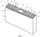
FIG. 1 is a perspective view of a battery cell having an overcharge protection device cover assembly in accordance with the present disclosure; -
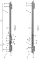
FIG. 2 is a cross-sectional view of a first embodiment of the overcharge protection device cover assembly in a normal operating condition in accordance with the present disclosure; -
FIG. 3 is a cross-sectional view of the first embodiment of the overcharge protection device cover assembly in an electrical short circuit condition in accordance with the present disclosure; -
FIG. 4 is a cross-sectional view of a second embodiment of an overcharge protection device cover assembly in a normal operating condition in accordance with the present disclosure; and -
FIG. 5 is a cross-sectional view of the second embodiment of the overcharge protection device cover assembly in an electrical short circuit condition in accordance with the present disclosure. - One or more specific embodiments will be described below. In an effort to provide a concise description of these embodiments, not all features of an actual implementation are described in the specification. It should be appreciated that in the development of any such actual implementation, as in any engineering or design project, numerous implementation-specific decisions must be made to achieve the developers' specific goals, such as compliance with system-related and business-related constraints, which may vary from one implementation to another. Moreover, it should be appreciated that such a development effort might be complex and time consuming, but would nevertheless be a routine undertaking of design, fabrication, and manufacture for those of ordinary skill having the benefit of this disclosure.
- Referring now to the drawings, an overcharge protection
device cover assembly 10 constructed in accordance with the principles of the present disclosure is shown inFIGS. 1-5 . The overcharge protectiondevice cover assembly 10 is shown coupled to abattery cell housing 12 inFIG. 1 . The overcharge protectiondevice cover assembly 10 and thebattery cell housing 12 are collectively referred to herein as abattery cell 14. In one embodiment, the overcharge protectiondevice cover assembly 10 includes abase plate 16 configured to be in contact with, adjacent, or coupled to thebattery cell housing 12, a first (or negative)terminal pad 18 in contact with a first (or negative)terminal 20, a second (or positive)terminal pad 22 in contact with a second (or positive)terminal 24, a reversal device 26 (reversal device 26 is not visible inFIG. 2 ), and aconductive element 28 between thereversal device 26 and the first 18 and second 22 terminal pads. In some embodiments theconductive element 28 is in the shape of disk, but other shapes can be used depending in design requirements, e.g., rectangle, square, etc. In some embodiments, thereversal device 26 is shaped in the form of a disk, but other shapes can be implemented depending on design requirements. In some embodiments, the reversal device is formed of a metal or polymer that allows the inner portion of thedeflection device 26 to deflect from a first position to a second position, the second position allowing activation of the overcharging protection by electrically short-circuiting the battery terminals. In one embodiment, the overcharge protectiondevice cover assembly 10 is configured to be coupled to a surface of thebattery cell housing 12 between the first 20 and second 24 terminals. In one embodiment, thereversal device 26 is integrated with, defined by, or coupled to thebase plate 16, and at least a portion of thereversal device 26 is deflectable. Further, thereversal device 26 may be composed of a more flexible material or may be thinner than thebase plate 16, such that internal pressure within thebattery cell housing 12 is able to deflect thereversal device 26 but not thebase plate 16. Theconductive element 28 is movable, at least in a linear direction that is orthogonal to, or at least substantially orthogonal to, thebase plate 16. However, it will be understood that thefirst terminal pad 18 andfirst terminal 20 may instead be a positive terminal pad and positive terminal, and thesecond terminal pad 22 andsecond terminal 24 may instead be a negative terminal pad and negative terminal. In some embodiments, the overcharge protectiondevice cover assembly 10 also includes avent aperture 30 configured to be aligned with a vent (not shown) in thebattery cell housing 12 when the overcharge protectiondevice cover assembly 10 is coupled to thebattery cell housing 12. In some embodiments, the overcharge protectiondevice cover assembly 10 also includes anelectrolyte aperture 32 to enable the addition of electrolyte to battery cell within thebattery cell housing 12. - The overcharge protection
device cover assembly 10 includes asymmetric first 18 and second 22 terminal pads. In one embodiment, thesecond terminal pad 22 has a length LSP that is less than a length LFP of the first terminal pad 18 (for example, as shown inFIG. 2 ). Alternatively, the firstterminal pad 18 may have a length LFP that is less than the length LSP of thesecond terminal pad 22. Further, the first 18 and second 22 terminal pads are in contact with or coupled to the first 20 and second 24 terminals, respectively. In one embodiment, thefirst terminal pad 18 includes afirst end portion 34 that is in contact with or coupled to thefirst terminal 20 and asecond end portion 36 opposite thefirst end portion 34. Thesecond end portion 36 is not coupled to any other component of the overcharge protectiondevice cover assembly 10, and is freely movable relative to thebase plate 16 in a linear direction that is crosswise (e.g., orthogonal) to thebase plate 16. Thus, thefirst end portion 34 of thefirst terminal pad 18 includes apivot point 38 at thefirst terminal 20 about which thefirst terminal pad 18 may move. Likewise, thesecond terminal pad 22 includes afirst end portion 40 that is in contact with or coupled to thesecond terminal 24 and asecond end portion 42 opposite thefirst end portion 40. Thesecond end portion 42 is not coupled to any other component of the overcharge protectiondevice cover assembly 10, and is freely movable relative to thebase plate 16 in a linear direction that is orthogonal to, or at least substantially orthogonal to, thebase plate 16. Thus, thefirst end portion 40 of thesecond terminal pad 22 includes apivot point 44 at thesecond terminal 24 about which thesecond terminal pad 22 may move. As such, the overcharge protectiondevice cover assembly 10 is transitionable from a first configuration (for example, as in a normal operating condition, as shown inFIGS. 2 and4 ) to a second configuration (for example, as in an electrical short circuit condition, as shown inFIGS. 3 and5 ). Although thesecond end portions base plate 16, it will be understood that thesecond end portions - Referring now to
FIGS. 2 and 3 , a first embodiment of an overcharge protectiondevice cover assembly 10 is shown. Thereversal device 26 is deflectable or transitionable between a first (inverted) configuration and a second (everted) configuration, and transition of thereversal device 26 between the first and second configurations causes the overcharge protectiondevice cover assembly 10 as a whole to transition between the first and second configurations. In a normal operating condition (e.g., before thereversal device 26 is deflected from an increase in internal pressure within the battery cell), as shown inFIG. 3 , the first 18 and second 22 terminal pads are uneven in height, although they each lie in a plane that is parallel to, or at least substantially parallel to, the plane in which thebase plate 16 lies. Thefirst terminal pad 18 includes a first (or upper)surface 46 and a second (or lower)surface 48 opposite thefirst surface 46. Likewise, thesecond terminal pad 22 includes a first (or upper)surface 50 and a second (or lower)surface 52 opposite thefirst surface 50. When the overcharge protectiondevice cover assembly 10 is in a normal operating condition (for example, as shown inFIG. 2 ), thefirst surface 46 of thefirst terminal pad 18 and thefirst surface 50 of thesecond terminal pad 22 are located at different distances from thebase plate 16, thereversal device 26, and theconductive element 28. Thesecond surface 48 of thefirst terminal pad 18 and thesecond surface 52 of thesecond terminal pad 22 are also located at different distances from thebase plate 16, thereversal device 26, and theconductive element 28. For example, thesecond surface 48 of thefirst terminal pad 18 is located a first distance DFP from thebase plate 16 and thesecond surface 52 of thesecond terminal pad 22 is located a second distance DSP from thebase plate 16. To accomplish this, the overcharge protectiondevice cover assembly 10 also includes a spacer plate 54 between thebase plate 16 and thefirst terminal pad 18, thereby positioning thefirst terminal pad 18 at a greater distance from thebase plate 16, thereversal device 26, and theconductive element 28. In one embodiment, the spacer plate 54 lies in a plane that is parallel to, or at least substantially parallel to, thebase plate 16. The cross-sectional view ofFIG. 2 shows that thefirst terminal pad 18 and thesecond terminal pad 22 are not coplanar when the overcharge protectiondevice cover assembly 10 is in the normal operating condition. - Further, each
terminal pad second end portion 36, 54 of eachterminal pad conductive element 28, at the location with which theconductive element 28 comes into contact with eachterminal pad device cover assembly 10 is in the short condition. In the embodiment shown inFIGS. 2 and 3 , the working thickness T of eachterminal pad - In an electrical short circuit condition (that is, after the
reversal device 26 is deflected from an increase in internal pressure within the battery cell), as shown inFIG. 3 , deflection of thereversal device 26 exerts a force against theconductive element 28, moving theconductive element 28 toward and into contact with thesecond surface 48 of thefirst terminal pad 18 and then thesecond surface 52 of thesecond terminal pad 22. As thesecond terminal pad 22 is located closer to thebase plate 16, thereversal device 26, and the conductive element 28 (due to the lack of a spacer plate 54 between thebase plate 16 and the second terminal pad 22), deflection of thereversal device 26 will cause theconductive element 28 to come into contact with thesecond surface 52 of thesecond terminal pad 22 before thesecond surface 48 of thefirst terminal pad 18. Additionally, as thesecond terminal pad 22 has a greater length LSP than the length LFP of thefirst terminal pad 18, thesecond terminal pad 22 is more easily pivoted at itspivot point 44 and moved linearly until at least a portion of thesecond end portion 42 of thesecond terminal pad 22 is at the same distance from thebase plate 16 as at least a portion of thesecond end portion 36 of the first terminal pad 18 (for example, as shown inFIG. 3 ). In one embodiment, at least a portion of thesecond surface 48 of thefirst terminal pad 18 and at least a portion of thesecond surface 52 of thesecond terminal pad 22 are aligned, as they are both in contact with theconductive element 28 when the overcharge protectiondevice cover assembly 10 is in the electrical short circuit condition. In the electrical short circuit condition, theconductive element 28 is in contact with both thefirst terminal pad 18 and thesecond terminal pad 22, establishing a short circuit to prevent the battery cell from overcharging. When theconductive element 28 is in contact with bothterminal pads second terminal pad 22 may be pivoted about itspivot point 44, thereby creating an angle between the plane in which thebase plate 16 lies and the plane in which thesecond terminal pad 22 lies. This angle may be very small, such as approximately 10° or less in some embodiments. Further, as thesecond end portion 36 of thefirst terminal pad 18 andsecond end portion 42 of thesecond terminal pad 22 are aligned when the overcharge protectiondevice cover assembly 10 is in the electrical short circuit condition andreversal device 26 is fully deflected (everted), with theconductive element 28 is at the its furthest distance from thebase plate 16, rather than when the overcharge protectiondevice cover assembly 10 is in the normal operating condition, much less precision is required during manufacture and assembly. Further, the configuration of the first 18 and second 22 terminal pads ensures theconductive element 28 will reliably contact bothterminal pads FIG. 3 shows that theterminal pads device cover assembly 10 is in the normal operating condition, and that at least a portion of each of thefirst surfaces terminal pads device cover assembly 10 is in the electrical short circuit condition, theterminal pads conductive element 28 contacts one of theterminal pads reversal device 26 deflects to move theconductive element 28 toward theterminal pads - Referring now to
FIGS. 4 and 5 , a second embodiment of an overcharge protectiondevice cover assembly 10 is shown. The second embodiment of the overcharge protectiondevice cover assembly 10 ofFIGS. 4 and 5 is similar to the first embodiment of the overcharge protectiondevice cover assembly 10 ofFIGS. 2 and 3 and, therefore, the same references numbers are used. However, unlike the first embodiment of the overcharge protectiondevice cover assembly 10, the second embodiment of the overcharge protectiondevice cover assembly 10 includes first 18 and second 22 terminal pads with different working thicknesses TFP and TSP at thesecond end portion 36 of thefirst terminal pad 18 proximate theconductive element 28 and at thesecond end portion 42 of thesecond terminal pad 22 proximate theconductive element 28. In one embodiment, thesecond terminal pad 22 has a working thickness TSP that is greater than the working thickness TFP of thefirst terminal pad 18. - When the overcharge protection
device cover assembly 10 is in the normal operating condition, the first 18 and second 22 terminal pads are uneven in height. That is, thefirst surface 46 of thefirst terminal pad 18 and thefirst surface 50 of thesecond terminal pad 22 are located at different distances from thebase plate 16, thereversal device 26, and theconductive element 28. Thesecond surface 48 of thefirst terminal pad 18 and thesecond surface 52 of thesecond terminal pad 22 are also located at different distances from thebase plate 16, thereversal device 26, and theconductive element 28. For example, thesecond surface 48 of thefirst terminal pad 18 is located a first distance DFP from thebase plate 16 and thesecond surface 52 of thesecond terminal pad 22 is located a second distance DSP from thebase plate 16. To accomplish this, the overcharge protectiondevice cover assembly 10 includes s spacer plate 54 between thebase plate 16 and thefirst terminal pad 18. The cross-sectional view ofFIG. 5 shows that thefirst terminal pad 18 and thesecond terminal pad 22 are not coplanar when the overcharge protectiondevice cover assembly 10 is in the normal operating condition. - In the electrical short circuit condition, as shown in
FIG. 5 , deflection of thereversal device 26 exerts a force against theconductive element 28, moving theconductive element 28 toward and into contact with thesecond surface 48 of thefirst terminal pad 18 and thesecond surface 52 of thesecond terminal pad 22. As thesecond terminal pad 22 is located closer to thebase plate 16, thereversal device 26, and the conductive element 28 (due to the lack of a spacer plate 54 between thebase plate 16 and the second terminal pad 22), deflection of thereversal device 26 will case theconductive element 28 to come into contact with thesecond surface 52 of thesecond terminal pad 22 before thesecond surface 48 of thefirst terminal pad 18. Additionally, as thesecond terminal pad 22 has a greater length LSP than the length LFP of thefirst terminal pad 18, thesecond terminal pad 22 is more easily pivoted at itspivot point 44 and moved linearly until at least a portion of thesecond end portion 42 of thesecond terminal pad 22 is at the same distance from thebase plate 16 as at least a portion of thesecond end portion 36 of the first terminal pad 18 (for example, as shown inFIG. 3 ). In one embodiment, at least a portion of thesecond surface 48 of thefirst terminal pad 18 and at least a portion of thesecond surface 52 of thesecond terminal pad 22 are aligned, as they are both in contact with theconductive element 28 when the overcharge protectiondevice cover assembly 10 is in the electrical short circuit condition. In the electrical short circuit condition, theconductive element 28 is in contact with both thefirst terminal pad 18 and thesecond terminal pad 22, establishing a short circuit to prevent the battery cell from overcharging. When theconductive element 28 is in contact with bothterminal pads second terminal pad 22 may be pivoted about itspivot point 44. Further, as thesecond end portion 36 of thefirst terminal pad 18 andsecond end portion 42 of thesecond terminal pad 22 are aligned when the overcharge protectiondevice cover assembly 10 is in the electrical short circuit condition andreversal device 26 is fully deflected (everted), with theconductive element 28 is at the its furthest distance from thebase plate 16, rather than when the overcharge protectiondevice cover assembly 10 is in the normal operating condition, much less precision is required during manufacture and assembly. Further, the configuration of the first 18 and second 22 terminal pads ensures theconductive element 28 will reliably contact bothterminal pads FIG. 2 shows that theterminal pads device cover assembly 10 is in the normal operating condition, and that at least a portion of each of thefirst surfaces terminal pads device cover assembly 10 is in the electrical short circuit condition, theterminal pads conductive element 28 contacts one of theterminal pads reversal device 26 deflects to move theconductive element 28 toward theterminal pads - An overcharge protection device cover assembly constructed in accordance with the principles of the present disclosure provides certain benefits over currently known overcharge protection devices. For example, the overcharge protection
device cover assemblies 10 disclosed herein each includeterminal pads base plate 16 andconductive element 28 when the overcharge protectiondevice cover assembly 10 is in a normal operating condition. This reduces manufacturing cost and complexity, as theterminal pads terminal pads second terminal pads 22 are longer than the first terminal pads 18) to allow thelonger terminal pad 22 to pivot more easily on itspivot point 44. During an electrical short circuit condition, deflection of thereversal device 26 causes theconductive element 28 to contact the longersecond terminal pad 22 before the shorterfirst terminal pad 18. When thereversal device 26 is fully deflected and theconductive element 28 has been moved to its farthest position from thebase plate 16, the first 18 and second 22 terminal pads are aligned. This configuration ensures that theconductive element 28 will reliably contact both the first 18 and second 22 terminal pads to establish a short circuit when overcharge protection is needed. In contrast, prior art overcharge protection devices require precisely aligned terminal pads for reliable overcharge protection, which increases manufacturing cost and complexity. - In one embodiment, an overcharge protection
device cover assembly 10 for use with abattery cell housing 12 havingfirst terminal 20 and asecond terminal 24 includes afirst terminal pad 18 having a first length LFP, thefirst terminal pad 18 being contactable with thefirst terminal 20 of thebattery cell housing 12, and asecond terminal pad 22 having a second length LSP that is greater than the first length LFP, thesecond terminal pad 22 being contactable with thesecond terminal 24 of thebattery cell housing 12. The overcharge protectiondevice cover assembly 10 also includes areversal device 26 that is deflectable toward the first 18 and second 22 terminal pads and aconductive element 28 between thereversal device 26 and the first 18 and second 22 terminal pads. - In one aspect of the embodiment, the
first terminal pad 18 includes afirst end portion 34 and asecond end portion 36 opposite thefirst end portion 34 and thesecond terminal pad 22 includes afirst end portion 40 and asecond end portion 42 opposite thefirst end portion 40, thefirst end portion 40 of thefirst terminal pad 18 being contactable with thefirst terminal 20 of thebattery cell housing 12 and thefirst end portion 40 of thesecond terminal pad 22 being contactable with thesecond terminal 24 of thebattery cell housing 12. In one aspect of the embodiment, thefirst terminal pad 18 includes afirst pivot point 38 about which thefirst terminal pad 18 is pivotable and thesecond terminal pad 22 includes asecond pivot point 44 about which thesecond terminal pad 22 is pivotable. In one aspect of the embodiment, the overcharge protectiondevice cover assembly 10 further includes abase plate 16, thebase plate 16 defining thereversal device 26, and a spacer plate 54 between thebase plate 16 and thefirst terminal pad 18. In one aspect of the embodiment, thesecond end portion 36 of thefirst terminal pad 18 and thesecond end portion 42 of thesecond terminal pad 22 are each movable in a direction that is orthogonal to a plant of thebase plate 16. - In one aspect of the embodiment, the
reversal device 26 is transitionable between a first configuration and a second configuration. In one aspect of the embodiment, thefirst terminal pad 18 is a first distance from thereversal device 26 when thereversal device 26 is in the first configuration and thesecond terminal pad 22 is a second distance from thereversal device 26 when thereversal device 26 is in the first configuration, the first distance being greater than the second distance. - In one aspect of the embodiment, each of the first and second terminal pads includes a working thickness T, the working thickness T of the first terminal pad and the working thickness T of the second terminal pad being the same.
- In one aspect of the embodiment, the
first terminal pad 18 includes a first working thickness TFP and thesecond terminal pad 22 includes a second working thickness TSP that is greater than the first working thickness TFP. - In one aspect of the embodiment, transition of the
reversal device 26 from the first configuration to the second configuration causes theconductive element 28 to contact thesecond terminal pad 22 before theconductive element 28 contacts thefirst terminal pad 18. - In one embodiment, an overcharge protection
device cover assembly 10 includes abase plate 16 including areversal device 26, thereversal device 26 being transitionable between a first configuration and a second configuration, afirst terminal pad 18 having a first length LFP, asecond terminal pad 22 having a second length LSP that is greater than the first length LFP, aconductive element 28 between thereversal device 26 and the first 18 and second 22 terminal pads, and a spacer plate 54 between thebase plate 16 and thefirst terminal pad 18. Thefirst terminal pad 18 is a first distance from thebase plate 16 when thereversal device 26 is in the first configuration and thesecond terminal pad 22 is a second distance from thebase plate 16 when thereversal device 26 is in the first configuration, the first distance being greater than the second distance. - In one aspect of the embodiment, each of the first and second terminal pads includes a working thickness T, the working thickness T of the first terminal pad and the working thickness T of the second terminal pad being the same.
- In one aspect of the embodiment, the
first terminal pad 18 includes a first working thickness TFP and thesecond terminal pad 22 includes a second working thickness TSP that is greater than the first working thickness TFP. - In one aspect of the embodiment, transition of the
reversal device 26 from the first configuration to the second configuration causes theconductive element 28 to contact thesecond terminal pad 22 before theconductive element 28 contacts thefirst terminal pad 18. - In one embodiment, a
battery cell 14 includes abattery cell housing 12, thebattery cell housing 12 includingfirst terminal 20 and asecond terminal 24, and an overcharge protectiondevice cover assembly 10 affixable to thebattery cell housing 12. The overcharge protectiondevice cover assembly 10 includes: abase plate 16 coupled to thebattery cell housing 12 between the first 32 and second 36 terminals, thebase plate 16 having areversal device 26 that is transitionable between a first configuration and a second configuration; afirst terminal pad 18 having afirst end portion 34, asecond end portion 36 opposite thefirst end portion 34, and a first length LFP, thefirst end portion 34 of thefirst terminal pad 18 being in contact with thefirst terminal 20; asecond terminal pad 22 having afirst end portion 40, asecond end portion 42 opposite thefirst end portion 40, and a second length LSP that is greater than the second length LFP, thefirst end portion 40 of thesecond terminal pad 22 being in contact with thesecond terminal 24; aconductive element 28 between thereversal device 26 and the first 30 and second 34 terminal pads; and a spacer plate 54 between thebase plate 16 and thefirst terminal pad 18. Thefirst terminal pad 18 is a first distance from thebase plate 16 when thereversal device 26 is in the first configuration and thesecond terminal pad 22 is a second distance from thebase plate 16 when thereversal device 26 is in the first configuration, the first distance being greater than the second distance. - In one aspect of the embodiment, the second end portion of each of the first and second terminal pads includes a working thickness T, the working thickness T of the second end portion of each of the first terminal pad and the working thickness T of the second terminal pad being the same.
- In one aspect of the embodiment, the second end portion of the
first terminal pad 18 has a first working thickness TFP and the second end portion of thesecond terminal pad 22 has a second working thickness TSP that is greater than the first working thickness TFP. - In one aspect of the embodiment, transition of the
reversal device 26 from the first configuration to the second configuration causes theconductive element 28 to contact thesecond terminal pad 22 before theconductive element 28 contacts thefirst terminal pad 18. - In one aspect of the embodiment, the
conductive element 28 is in contact with the first 30 and second 34 terminal pads when theconductive element 28 is in the second configuration. In one aspect of the embodiment, a short circuit is established in thebattery cell 14 when theconductive element 28 is in the second configuration. - One or more of the disclosed embodiments, alone or in combination, may provide one or more technical effects useful in the manufacture of battery cells, and portions of battery cells. The disclosed embodiments relate to battery cells that include an overcharge protection assembly. The overcharge protection assembly may include a reversal device that is activated when a pressure in a casing of the battery cell reaches a threshold value. The activation of the reversal device may cause electrical contact between terminals of the battery cell, which may create an external circuit by electrically coupling the positive terminal and the negative terminal of the battery cell. Such an external short circuit may discharge the battery cell, but the external short circuit may prevent thermal runaway and/or permanent damage to the battery cell. Additionally or alternatively, the short circuit may cause a large amount of current to be transmitted through an internal current collector of the battery cell, which may cause the current collector to melt and thereby cut the flow of electric current. It should be noted that the embodiments described in the specification may have other technical effects and can solve other technical problems.
The specific embodiments described above have been shown by way of example, and it should be understood that these embodiments may be susceptible to various modifications and alternative forms within the scope as defined by the appended claims. It should be further understood that the claims are not intended to be limited to the particular forms disclosed.
Claims (13)
- An overcharge protection device cover assembly (10) for use with a battery cell housing, the battery cell housing (12) having a first terminal (20) and a second terminal (24), the overcharge protection device cover assembly (10) comprising:- a first terminal pad (18) having a first length (LFP), the first terminal pad (18) being contactable with the first terminal (20) of the battery cell housing (12);- a second terminal pad (22) having a second length (LSP) that is greater than the first length (LFP), the second terminal pad (22) being contactable with the second terminal (24) of the battery cell housing (12);- a reversal device (26) that is deflectable toward the first and second terminal pads (18, 22); and- a conductive element (28) between the reversal device (26) and the first and second terminal pads (18, 22),wherein the reversal device (26) is configured to transition between a first configuration and a second configuration, wherein the first terminal pad (18) is a first distance (DFP) from the reversal device (26) when the reversal device (26) is in the first configuration and the second terminal pad (22) is a second distance (DSP) from the reversal device (26) when the reversal device (26) is in the first configuration, the first distance (DFP) being greater than the second distance (DSP),wherein transition of the reversal device (26) from the first configuration to the second configuration causes the conductive element (28) to contact the second terminal pad (22) before the conductive element (28) contacts the first terminal pad (18).
- The overcharge protection device cover assembly (10) of claim 1, wherein:- the first terminal pad (18) includes a first end portion (34) and a second end portion (36) opposite the first end portion (34);- the second terminal pad (22) includes a first end portion (40) and a second end portion (42) opposite the first end portion (40),- the first end portion (34) of the first terminal pad (18) being contactable with the first terminal (20) of the battery cell housing (12) and the first end portion (40) of the second terminal pad (22) being contactable with the second terminal (24) of the battery cell housing (12).
- The overcharge protection device cover assembly (10) of claim 2,
wherein the first terminal pad (18) includes a first pivot point (38) about which the first terminal pad (18) is pivotable and the second terminal pad (22) includes a second pivot point (44) about which the second terminal pad (22) is pivotable. - The overcharge protection device cover assembly (10) of claim 3, further comprising:- a base plate (16), the base plate (16) defining the reversal device (26); and- a spacer plate (54) between the base plate (16) and the first terminal pad (18).
- The overcharge protection device cover assembly (10) of claim 4,
wherein the second end portion (36) of the first terminal pad (18) and the second end portion (42) of the second terminal pad (22) are each movable in a direction that is orthogonal to a plane of the base plate (16). - The overcharge protection device cover assembly (10) of claim 1,
wherein each of the first and second terminal pads (18, 22) includes a working thickness (T), the working thickness (T) of the first terminal pad (18) and the working thickness (T) of the second terminal pad (22) being the same. - The overcharge protection device cover assembly (10) of claim 1,
wherein the first terminal pad (18) includes a first working thickness (TFP) and the second terminal pad (22) includes a second working thickness (TSP) that is greater than the first working thickness (TFP). - An overcharge protection device cover assembly (10), the overcharge protection device cover assembly (10) comprising:- a base plate (16) including a reversal device (26), the reversal device (26) being transitionable between a first configuration and a second configuration;- a first terminal pad (18) having a first length (LFP);- a second terminal pad (22) having a second length (LSP) that is greater than the first length (LFP);- a conductive element (28) between the reversal device (26) and the first and second terminal pads (18, 22); and- a spacer plate (54) between the base plate (16) and the first terminal pad (18), thereby positioning the first terminal pad (18) at a greater distance from the base plate (16), the reversal device (26), and the conductive element (28), the first terminal pad (18) being a first distance (DFP) from the base plate (16) when the reversal device (26) is in the first configuration and the second terminal pad (22) being a second distance (DSP) from the base plate (16) when the reversal device (26) is in the first configuration, the first distance (DFP) being greater than the second distance (DSP),wherein transition of the reversal device (26) from the first configuration to the second configuration causes the conductive element (28) to contact the second terminal pad (22) before the conductive element (28) contacts the first terminal pad (18).
- The overcharge protection device cover assembly (10) of claim 8,
wherein each of the first and second terminal pads (18, 22) includes a working thickness (T), the working thickness (T) of the first terminal pad (18) and the working thickness (T) of the second terminal pad (22) being the same. - The overcharge protection device cover assembly (10) of claim 8,
wherein the first terminal pad (18) includes a first working thickness (TFP) and the second terminal pad (22) includes a second working thickness (TSP) that is greater than the first working thickness (TFP). - A battery cell (14) comprising:- a battery cell housing (12), the battery cell housing (12) including first terminal (20) and a second terminal (24); and- an overcharge protection device cover assembly (10) affixable to the battery cell housing (12), the overcharge protection device cover assembly (10) being an overcharge protection device cover assembly (10) according to any one of claims 8 to 10.
- The battery cell (14) of claim 11,
wherein the conductive element (28) is in contact with the first and second terminal pads (18, 22) when the conductive element (28) is in the second configuration. - The battery cell of claim 12,
wherein a short circuit is established in the battery cell (14) when the conductive element (28) is in the second configuration.
Applications Claiming Priority (2)
| Application Number | Priority Date | Filing Date | Title |
|---|---|---|---|
| US201762588581P | 2017-11-20 | 2017-11-20 | |
| PCT/US2018/062121 WO2019100076A1 (en) | 2017-11-20 | 2018-11-20 | Overcharge protection device with uneven terminal pads |
Publications (2)
| Publication Number | Publication Date |
|---|---|
| EP3714496A1 EP3714496A1 (en) | 2020-09-30 |
| EP3714496B1 true EP3714496B1 (en) | 2025-04-23 |
Family
ID=64650572
Family Applications (1)
| Application Number | Title | Priority Date | Filing Date |
|---|---|---|---|
| EP18815485.0A Active EP3714496B1 (en) | 2017-11-20 | 2018-11-20 | Overcharge protection device with uneven terminal pads |
Country Status (4)
| Country | Link |
|---|---|
| US (2) | US11539103B2 (en) |
| EP (1) | EP3714496B1 (en) |
| CN (2) | CN116799384A (en) |
| WO (1) | WO2019100076A1 (en) |
Families Citing this family (1)
| Publication number | Priority date | Publication date | Assignee | Title |
|---|---|---|---|---|
| WO2019100076A1 (en) | 2017-11-20 | 2019-05-23 | Johnson Controls Technology Company | Overcharge protection device with uneven terminal pads |
Family Cites Families (18)
| Publication number | Priority date | Publication date | Assignee | Title |
|---|---|---|---|---|
| JP3081847B1 (en) * | 1999-02-01 | 2000-08-28 | エヌイーシーモバイルエナジー株式会社 | Sealed battery |
| JP2002043366A (en) * | 2000-07-21 | 2002-02-08 | Canon Inc | Semiconductor device |
| JP4629952B2 (en) * | 2002-02-13 | 2011-02-09 | パナソニック株式会社 | Manufacturing method of secondary battery |
| KR100920207B1 (en) * | 2006-11-27 | 2009-10-06 | 주식회사 엘지화학 | Power switching module for manufacturing battery module assembly |
| US8877361B2 (en) * | 2009-09-01 | 2014-11-04 | Samsung Sdi Co., Ltd. | Rechargeable battery |
| US20120015242A1 (en) * | 2010-07-16 | 2012-01-19 | Coda Automotive, Inc. | Battery with improved terminals |
| US9112292B2 (en) * | 2012-03-16 | 2015-08-18 | Makita Corporation | Terminal structure |
| CN203039014U (en) * | 2013-01-21 | 2013-07-03 | 宁德新能源科技有限公司 | Power battery |
| DE102013204319A1 (en) * | 2013-03-13 | 2014-09-18 | Robert Bosch Gmbh | Safety device for a galvanic cell |
| KR20140115756A (en) * | 2013-03-22 | 2014-10-01 | 삼성에스디아이 주식회사 | Protection apparatus of battery pack and method for manufacturing the same and battery pack having the same |
| CN203165987U (en) * | 2013-04-09 | 2013-08-28 | 宁德时代新能源科技有限公司 | Lithium-ion battery and safety overturning valve for over-charging safety protection device of lithium-ion battery |
| KR20150042618A (en) * | 2013-10-11 | 2015-04-21 | 삼성에스디아이 주식회사 | Rechargeable battery |
| US20150104672A1 (en) | 2013-10-16 | 2015-04-16 | Ningde Contemporary Amperex Technology Limited | Safety device of lithium-ion battery |
| JP2016081714A (en) * | 2014-10-16 | 2016-05-16 | 株式会社東芝 | Storage battery device and thermostat |
| US9741997B2 (en) * | 2014-11-05 | 2017-08-22 | Samsung Sdi Co., Ltd. | Rechargeable battery |
| CN206134740U (en) * | 2016-08-11 | 2017-04-26 | 宁德时代新能源科技股份有限公司 | Power battery and power battery safety top cover |
| CN106450475B (en) * | 2016-11-15 | 2019-08-02 | 宁德时代新能源科技股份有限公司 | Secondary battery and battery module |
| WO2019100076A1 (en) | 2017-11-20 | 2019-05-23 | Johnson Controls Technology Company | Overcharge protection device with uneven terminal pads |
-
2018
- 2018-11-20 WO PCT/US2018/062121 patent/WO2019100076A1/en not_active Ceased
- 2018-11-20 CN CN202310858932.9A patent/CN116799384A/en active Pending
- 2018-11-20 US US16/764,324 patent/US11539103B2/en active Active
- 2018-11-20 CN CN201880072984.0A patent/CN111344882B/en active Active
- 2018-11-20 EP EP18815485.0A patent/EP3714496B1/en active Active
-
2022
- 2022-12-26 US US18/088,737 patent/US12107302B2/en active Active
Also Published As
| Publication number | Publication date |
|---|---|
| CN111344882A (en) | 2020-06-26 |
| EP3714496A1 (en) | 2020-09-30 |
| CN116799384A (en) | 2023-09-22 |
| CN111344882B (en) | 2023-07-25 |
| US12107302B2 (en) | 2024-10-01 |
| US20230126939A1 (en) | 2023-04-27 |
| WO2019100076A1 (en) | 2019-05-23 |
| US11539103B2 (en) | 2022-12-27 |
| US20200280046A1 (en) | 2020-09-03 |
Similar Documents
| Publication | Publication Date | Title |
|---|---|---|
| JP7190712B2 (en) | battery module | |
| JP5415888B2 (en) | battery pack | |
| KR102066198B1 (en) | Battery pack | |
| KR102317503B1 (en) | Battery Pack | |
| JP2009231138A (en) | Battery pack | |
| KR20050095949A (en) | Cap assembly and secondary battery thereof | |
| US8658294B2 (en) | Protective circuit module and secondary battery having the same | |
| KR20140137180A (en) | Rechargeable battery | |
| CN107799709B (en) | rechargeable battery | |
| US8778518B2 (en) | Battery pack | |
| KR20160020284A (en) | Battery pack | |
| EP2600434A1 (en) | Battery module | |
| KR20170040636A (en) | Battery module and battery pack including the same | |
| US12107302B2 (en) | Overcharge protection device with uneven terminal pads | |
| KR20140081105A (en) | Cap Assembly Having Electrode Terminal Protection Member and Battery Cell Comprising the Same | |
| CN109891636B (en) | Battery module and battery pack including the same | |
| CN107170947B (en) | Secondary battery and secondary battery assembly | |
| KR20010095528A (en) | Secondary battery having protective case | |
| EP4087012A1 (en) | Battery module, and battery pack and vehicle which comprise same | |
| EP3531478B1 (en) | Current blocking structure applied to pouch type secondary battery | |
| KR102703641B1 (en) | Current short device, secondary battery including the same and battery module | |
| KR20160147346A (en) | Prismatic Battery Pack Having External Input Output Positive Electrode Protruded Outside | |
| EP4336639B1 (en) | Battery module and battery pack and vehicle comprising same | |
| KR20220102023A (en) | Battery pack including a member capable of preventing poor contact with the device |
Legal Events
| Date | Code | Title | Description |
|---|---|---|---|
| STAA | Information on the status of an ep patent application or granted ep patent |
Free format text: STATUS: UNKNOWN |
|
| STAA | Information on the status of an ep patent application or granted ep patent |
Free format text: STATUS: THE INTERNATIONAL PUBLICATION HAS BEEN MADE |
|
| PUAI | Public reference made under article 153(3) epc to a published international application that has entered the european phase |
Free format text: ORIGINAL CODE: 0009012 |
|
| STAA | Information on the status of an ep patent application or granted ep patent |
Free format text: STATUS: REQUEST FOR EXAMINATION WAS MADE |
|
| 17P | Request for examination filed |
Effective date: 20200612 |
|
| AK | Designated contracting states |
Kind code of ref document: A1 Designated state(s): AL AT BE BG CH CY CZ DE DK EE ES FI FR GB GR HR HU IE IS IT LI LT LU LV MC MK MT NL NO PL PT RO RS SE SI SK SM TR |
|
| AX | Request for extension of the european patent |
Extension state: BA ME |
|
| DAV | Request for validation of the european patent (deleted) | ||
| DAX | Request for extension of the european patent (deleted) | ||
| STAA | Information on the status of an ep patent application or granted ep patent |
Free format text: STATUS: EXAMINATION IS IN PROGRESS |
|
| 17Q | First examination report despatched |
Effective date: 20240531 |
|
| REG | Reference to a national code |
Ref country code: DE Ref legal event code: R079 Free format text: PREVIOUS MAIN CLASS: H01M0002340000 Ipc: H01M0050578000 Ref country code: DE Ref legal event code: R079 Ref document number: 602018081355 Country of ref document: DE Free format text: PREVIOUS MAIN CLASS: H01M0002340000 Ipc: H01M0050578000 |
|
| GRAP | Despatch of communication of intention to grant a patent |
Free format text: ORIGINAL CODE: EPIDOSNIGR1 |
|
| STAA | Information on the status of an ep patent application or granted ep patent |
Free format text: STATUS: GRANT OF PATENT IS INTENDED |
|
| RIC1 | Information provided on ipc code assigned before grant |
Ipc: H01M 50/578 20210101AFI20241218BHEP |
|
| INTG | Intention to grant announced |
Effective date: 20250109 |
|
| GRAS | Grant fee paid |
Free format text: ORIGINAL CODE: EPIDOSNIGR3 |
|
| GRAA | (expected) grant |
Free format text: ORIGINAL CODE: 0009210 |
|
| STAA | Information on the status of an ep patent application or granted ep patent |
Free format text: STATUS: THE PATENT HAS BEEN GRANTED |
|
| AK | Designated contracting states |
Kind code of ref document: B1 Designated state(s): AL AT BE BG CH CY CZ DE DK EE ES FI FR GB GR HR HU IE IS IT LI LT LU LV MC MK MT NL NO PL PT RO RS SE SI SK SM TR |
|
| REG | Reference to a national code |
Ref country code: GB Ref legal event code: FG4D |
|
| REG | Reference to a national code |
Ref country code: CH Ref legal event code: EP |
|
| REG | Reference to a national code |
Ref country code: DE Ref legal event code: R096 Ref document number: 602018081355 Country of ref document: DE |
|
| REG | Reference to a national code |
Ref country code: IE Ref legal event code: FG4D |
|
| REG | Reference to a national code |
Ref country code: NL Ref legal event code: MP Effective date: 20250423 |
|
| PG25 | Lapsed in a contracting state [announced via postgrant information from national office to epo] |
Ref country code: NL Free format text: LAPSE BECAUSE OF FAILURE TO SUBMIT A TRANSLATION OF THE DESCRIPTION OR TO PAY THE FEE WITHIN THE PRESCRIBED TIME-LIMIT Effective date: 20250423 |
|
| REG | Reference to a national code |
Ref country code: AT Ref legal event code: MK05 Ref document number: 1788733 Country of ref document: AT Kind code of ref document: T Effective date: 20250423 |
|
| PG25 | Lapsed in a contracting state [announced via postgrant information from national office to epo] |
Ref country code: PT Free format text: LAPSE BECAUSE OF FAILURE TO SUBMIT A TRANSLATION OF THE DESCRIPTION OR TO PAY THE FEE WITHIN THE PRESCRIBED TIME-LIMIT Effective date: 20250825 Ref country code: FI Free format text: LAPSE BECAUSE OF FAILURE TO SUBMIT A TRANSLATION OF THE DESCRIPTION OR TO PAY THE FEE WITHIN THE PRESCRIBED TIME-LIMIT Effective date: 20250423 Ref country code: ES Free format text: LAPSE BECAUSE OF FAILURE TO SUBMIT A TRANSLATION OF THE DESCRIPTION OR TO PAY THE FEE WITHIN THE PRESCRIBED TIME-LIMIT Effective date: 20250423 |
|
| REG | Reference to a national code |
Ref country code: LT Ref legal event code: MG9D |
|
| PG25 | Lapsed in a contracting state [announced via postgrant information from national office to epo] |
Ref country code: NO Free format text: LAPSE BECAUSE OF FAILURE TO SUBMIT A TRANSLATION OF THE DESCRIPTION OR TO PAY THE FEE WITHIN THE PRESCRIBED TIME-LIMIT Effective date: 20250723 Ref country code: GR Free format text: LAPSE BECAUSE OF FAILURE TO SUBMIT A TRANSLATION OF THE DESCRIPTION OR TO PAY THE FEE WITHIN THE PRESCRIBED TIME-LIMIT Effective date: 20250724 |
|
| PG25 | Lapsed in a contracting state [announced via postgrant information from national office to epo] |
Ref country code: PL Free format text: LAPSE BECAUSE OF FAILURE TO SUBMIT A TRANSLATION OF THE DESCRIPTION OR TO PAY THE FEE WITHIN THE PRESCRIBED TIME-LIMIT Effective date: 20250423 |
|
| PG25 | Lapsed in a contracting state [announced via postgrant information from national office to epo] |
Ref country code: BG Free format text: LAPSE BECAUSE OF FAILURE TO SUBMIT A TRANSLATION OF THE DESCRIPTION OR TO PAY THE FEE WITHIN THE PRESCRIBED TIME-LIMIT Effective date: 20250423 |
|
| PG25 | Lapsed in a contracting state [announced via postgrant information from national office to epo] |
Ref country code: HR Free format text: LAPSE BECAUSE OF FAILURE TO SUBMIT A TRANSLATION OF THE DESCRIPTION OR TO PAY THE FEE WITHIN THE PRESCRIBED TIME-LIMIT Effective date: 20250423 |
|
| PG25 | Lapsed in a contracting state [announced via postgrant information from national office to epo] |
Ref country code: AT Free format text: LAPSE BECAUSE OF FAILURE TO SUBMIT A TRANSLATION OF THE DESCRIPTION OR TO PAY THE FEE WITHIN THE PRESCRIBED TIME-LIMIT Effective date: 20250423 |
|
| PG25 | Lapsed in a contracting state [announced via postgrant information from national office to epo] |
Ref country code: RS Free format text: LAPSE BECAUSE OF FAILURE TO SUBMIT A TRANSLATION OF THE DESCRIPTION OR TO PAY THE FEE WITHIN THE PRESCRIBED TIME-LIMIT Effective date: 20250723 |
|
| PG25 | Lapsed in a contracting state [announced via postgrant information from national office to epo] |
Ref country code: IS Free format text: LAPSE BECAUSE OF FAILURE TO SUBMIT A TRANSLATION OF THE DESCRIPTION OR TO PAY THE FEE WITHIN THE PRESCRIBED TIME-LIMIT Effective date: 20250823 |
|
| PG25 | Lapsed in a contracting state [announced via postgrant information from national office to epo] |
Ref country code: LV Free format text: LAPSE BECAUSE OF FAILURE TO SUBMIT A TRANSLATION OF THE DESCRIPTION OR TO PAY THE FEE WITHIN THE PRESCRIBED TIME-LIMIT Effective date: 20250423 |
|
| PGFP | Annual fee paid to national office [announced via postgrant information from national office to epo] |
Ref country code: DE Payment date: 20251128 Year of fee payment: 8 |
|
| PGFP | Annual fee paid to national office [announced via postgrant information from national office to epo] |
Ref country code: GB Payment date: 20251127 Year of fee payment: 8 |
|
| PG25 | Lapsed in a contracting state [announced via postgrant information from national office to epo] |
Ref country code: SM Free format text: LAPSE BECAUSE OF FAILURE TO SUBMIT A TRANSLATION OF THE DESCRIPTION OR TO PAY THE FEE WITHIN THE PRESCRIBED TIME-LIMIT Effective date: 20250423 Ref country code: DK Free format text: LAPSE BECAUSE OF FAILURE TO SUBMIT A TRANSLATION OF THE DESCRIPTION OR TO PAY THE FEE WITHIN THE PRESCRIBED TIME-LIMIT Effective date: 20250423 |
|
| PGFP | Annual fee paid to national office [announced via postgrant information from national office to epo] |
Ref country code: FR Payment date: 20251125 Year of fee payment: 8 |
|
| PG25 | Lapsed in a contracting state [announced via postgrant information from national office to epo] |
Ref country code: CZ Free format text: LAPSE BECAUSE OF FAILURE TO SUBMIT A TRANSLATION OF THE DESCRIPTION OR TO PAY THE FEE WITHIN THE PRESCRIBED TIME-LIMIT Effective date: 20250423 |
|
| PG25 | Lapsed in a contracting state [announced via postgrant information from national office to epo] |
Ref country code: EE Free format text: LAPSE BECAUSE OF FAILURE TO SUBMIT A TRANSLATION OF THE DESCRIPTION OR TO PAY THE FEE WITHIN THE PRESCRIBED TIME-LIMIT Effective date: 20250423 |
|
| REG | Reference to a national code |
Ref country code: DE Ref legal event code: R097 Ref document number: 602018081355 Country of ref document: DE |
|
| PG25 | Lapsed in a contracting state [announced via postgrant information from national office to epo] |
Ref country code: SK Free format text: LAPSE BECAUSE OF FAILURE TO SUBMIT A TRANSLATION OF THE DESCRIPTION OR TO PAY THE FEE WITHIN THE PRESCRIBED TIME-LIMIT Effective date: 20250423 Ref country code: RO Free format text: LAPSE BECAUSE OF FAILURE TO SUBMIT A TRANSLATION OF THE DESCRIPTION OR TO PAY THE FEE WITHIN THE PRESCRIBED TIME-LIMIT Effective date: 20250423 |
|
| PG25 | Lapsed in a contracting state [announced via postgrant information from national office to epo] |
Ref country code: IT Free format text: LAPSE BECAUSE OF FAILURE TO SUBMIT A TRANSLATION OF THE DESCRIPTION OR TO PAY THE FEE WITHIN THE PRESCRIBED TIME-LIMIT Effective date: 20250423 |
|
| PLBE | No opposition filed within time limit |
Free format text: ORIGINAL CODE: 0009261 |
|
| STAA | Information on the status of an ep patent application or granted ep patent |
Free format text: STATUS: NO OPPOSITION FILED WITHIN TIME LIMIT |
|
| REG | Reference to a national code |
Ref country code: CH Ref legal event code: L10 Free format text: ST27 STATUS EVENT CODE: U-0-0-L10-L00 (AS PROVIDED BY THE NATIONAL OFFICE) Effective date: 20260304 |
|
| 26N | No opposition filed |
Effective date: 20260126 |