EP3713222A1 - Image sensor and manufacture method therefor and electronic device - Google Patents
Image sensor and manufacture method therefor and electronic device Download PDFInfo
- Publication number
- EP3713222A1 EP3713222A1 EP19813403.3A EP19813403A EP3713222A1 EP 3713222 A1 EP3713222 A1 EP 3713222A1 EP 19813403 A EP19813403 A EP 19813403A EP 3713222 A1 EP3713222 A1 EP 3713222A1
- Authority
- EP
- European Patent Office
- Prior art keywords
- circuit
- pixel array
- module
- signal processing
- image sensor
- Prior art date
- Legal status (The legal status is an assumption and is not a legal conclusion. Google has not performed a legal analysis and makes no representation as to the accuracy of the status listed.)
- Ceased
Links
Images



Classifications
-
- H—ELECTRICITY
- H10—SEMICONDUCTOR DEVICES; ELECTRIC SOLID-STATE DEVICES NOT OTHERWISE PROVIDED FOR
- H10F—INORGANIC SEMICONDUCTOR DEVICES SENSITIVE TO INFRARED RADIATION, LIGHT, ELECTROMAGNETIC RADIATION OF SHORTER WAVELENGTH OR CORPUSCULAR RADIATION
- H10F39/00—Integrated devices, or assemblies of multiple devices, comprising at least one element covered by group H10F30/00, e.g. radiation detectors comprising photodiode arrays
- H10F39/80—Constructional details of image sensors
- H10F39/809—Constructional details of image sensors of hybrid image sensors
-
- H—ELECTRICITY
- H04—ELECTRIC COMMUNICATION TECHNIQUE
- H04N—PICTORIAL COMMUNICATION, e.g. TELEVISION
- H04N25/00—Circuitry of solid-state image sensors [SSIS]; Control thereof
- H04N25/70—SSIS architectures; Circuits associated therewith
- H04N25/76—Addressed sensors, e.g. MOS or CMOS sensors
- H04N25/78—Readout circuits for addressed sensors, e.g. output amplifiers or A/D converters
-
- H—ELECTRICITY
- H04—ELECTRIC COMMUNICATION TECHNIQUE
- H04N—PICTORIAL COMMUNICATION, e.g. TELEVISION
- H04N25/00—Circuitry of solid-state image sensors [SSIS]; Control thereof
- H04N25/70—SSIS architectures; Circuits associated therewith
- H04N25/79—Arrangements of circuitry being divided between different or multiple substrates, chips or circuit boards, e.g. stacked image sensors
-
- H—ELECTRICITY
- H10—SEMICONDUCTOR DEVICES; ELECTRIC SOLID-STATE DEVICES NOT OTHERWISE PROVIDED FOR
- H10F—INORGANIC SEMICONDUCTOR DEVICES SENSITIVE TO INFRARED RADIATION, LIGHT, ELECTROMAGNETIC RADIATION OF SHORTER WAVELENGTH OR CORPUSCULAR RADIATION
- H10F39/00—Integrated devices, or assemblies of multiple devices, comprising at least one element covered by group H10F30/00, e.g. radiation detectors comprising photodiode arrays
- H10F39/011—Manufacture or treatment of image sensors covered by group H10F39/12
- H10F39/018—Manufacture or treatment of image sensors covered by group H10F39/12 of hybrid image sensors
-
- H—ELECTRICITY
- H10—SEMICONDUCTOR DEVICES; ELECTRIC SOLID-STATE DEVICES NOT OTHERWISE PROVIDED FOR
- H10F—INORGANIC SEMICONDUCTOR DEVICES SENSITIVE TO INFRARED RADIATION, LIGHT, ELECTROMAGNETIC RADIATION OF SHORTER WAVELENGTH OR CORPUSCULAR RADIATION
- H10F39/00—Integrated devices, or assemblies of multiple devices, comprising at least one element covered by group H10F30/00, e.g. radiation detectors comprising photodiode arrays
- H10F39/80—Constructional details of image sensors
- H10F39/811—Interconnections
Definitions
- the present application relate to the field of image sensor, and in particular, to an image sensor, a manufacturing method thereof and an electronic device.
- the cost per unit area of the chip is determined by the portion corresponding to the highest cost per unit area.
- a pixel array (pixel array) unit and a signal processing unit are included, where the pixel array unit occupies most of the area of the chip, while the signal processing unit occupies a small area.
- the pixel array unit has a small device type and a low process requirement, and thus the cost per unit area corresponding to the pixel array unit is relatively low.
- the signal processing unit includes a variety of device types, which requires a more complicated process, and thus the cost per unit area corresponding to the signal processing unit is relatively high.
- the cost per unit area of the chip is generally determined by the cost per unit area of the signal processing unit, and the total cost of the chip is high.
- Embodiments of the present application provide an image sensor and a manufacturing method thereof, and an electronic device, which is capable of reducing the cost of the image sensor.
- an image sensor including: a pixel array module disposed on a first wafer; a signal processing module disposed on a second wafer; an electrical connection module connecting the pixel array module and the signal processing module; where the pixel array module is configured to receive an optical signal and convert the optical signal into an electrical signal, and the signal processing module is configured to process the electrical signal.
- devices of the image sensor are disposed on two wafers, and the connection is realized by electrical connection between the two wafers, which can reduce the cost of the image sensor.
- devices in the pixel array module consist of analog devices, and devices in the signal processing module includes digital devices.
- the pixel array module consisting of analog devices is disposed on a single wafer, which may reduce the cost of the module.
- the pixel array module includes a first metal interconnect layer of a first predetermined number, the first metal interconnect layer is configured for interconnection of the devices in the pixel array module, and the first predetermined number is less than or equal to 4.
- the first metal interconnect layer is connected to the electrical connection module.
- the signal processing module includes a second metal interconnect layer of a first predetermined number, the second metal interconnect layer is configured for interconnection of the devices in the signal processing module, and the second predetermined number is greater than or equal to 4.
- the second metal interconnect layer is connected to the electrical connection module.
- the pixel array module includes a pixel array circuit including a plurality of pixel sensitive units configured to receive the optical signal and convert the optical signal into the electrical signal.
- the pixel array module further includes a row and column control circuit configured to receive a control signal generated by the signal processing module, and to control the plurality of pixel sensitive units for receiving the optical signal and converting the optical signal to the electrical signal.
- the pixel array module further includes a readout circuit configured to receive the electrical signal output by the plurality of pixel sensitive units and send the electrical signal to the signal processing module.
- the readout circuit includes an amplifying circuit configured to amplify the electrical signal output by the plurality of pixel sensitive units.
- the signal processing module includes an analog to digital conversion circuit configured to receive the electrical signal generated by the pixel array module and convert the electrical signal into a digital electrical signal.
- the signal processing module further includes a digital processing circuit configured to receive the digital electrical signal generated by the analog to digital conversion circuit and process the digital electrical signal.
- the signal processing module further includes a logic control circuit configured to generate a control signal.
- the signal processing module further includes a storage circuit configured to store a particular signal, where the particular signal includes a signal processed by the digital processing circuit.
- the analog to digital conversion circuit is connected to the amplifying circuit through the electrical connection module, and the logic control circuit is connected to the row and column control circuit and the readout circuit through the electrical connection module.
- the electrical connection module between the two wafers is disposed between the analog to digital conversion circuit and the amplifying circuit, and between the logic control circuit and the row and column control circuit and the readout circuit. With this arrangement, the implementation complexity of the electrical connection module between the two wafers can be reduced.
- the electrical connection module is configured to transmit the electrical signal generated by the pixel array module and a control signal generated by the signal processing module.
- the electrical connection module includes a wire bonding apparatus.
- the first wafer and the second wafer are epitaxial wafers or standard wafers.
- the first wafer and the second wafer are disposed in stack.
- a manufacturing method of an image sensor including:
- devices in the pixel array module consist of analog devices, and devices in the signal processing module include digital devices.
- the pixel array module includes a first metal interconnect layer of a first predetermined number, the devices in the pixel array module are interconnected through the first metal interconnect layer, and the first predetermined number is less than or equal to 4.
- the pixel array module is connected to the electrical connection module through the first metal interconnect layer.
- the pixel array module includes a pixel array circuit including a plurality of pixel sensitive units.
- the pixel array module includes a row control circuit and a column control circuit, where the row control circuit is connected to a pixel sensitive unit row in the pixel array circuit through the first metal interconnect layer, and the column control circuit is connected to a pixel sensitive unit column in the pixel array circuit through the first metal interconnect layer.
- the row control circuit and the column control circuit are connected to the electrical connection module through the first metal interconnect layer.
- the pixel array module further includes a readout circuit connected to the column control circuit and the electrical connection module through the first metal interconnect layer.
- the readout circuit includes an amplifying circuit connected to the column control circuit and the electrical connection module through the first metal interconnect layer.
- the signal processing module includes a second metal interconnect layer of a second predetermined number, the devices in the signal processing module are interconnected through the second metal interconnect layer, and the second predetermined number is greater than or equal to 4.
- the signal processing module is connected to the electrical connection module through the second metal interconnect layer.
- the signal processing module includes an analog to digital conversion circuit connected to the electrical connection module through the second metal interconnect layer.
- the signal processing module further includes a digital processing circuit connected to the analog to digital conversion circuit through the second metal interconnect layer.
- the signal processing module further includes a logic control circuit connected to the analog to digital conversion circuit, the digital processing circuit, the storage circuit, and the electrical connection module through the second metal interconnect layer.
- the signal processing module further includes a storage circuit configured to be connected to the digital processing circuit through the second metal interconnect layer.
- the analog to digital conversion signal is connected to the readout circuit through the electrical connection module, and the logic control circuit is connected to the row control circuit, the column control circuit, and the readout circuit through the electrical connection module.
- the electrical connection module includes a wire bonding apparatus.
- the first wafer and the second wafer are epitaxial wafers or standard wafers.
- the first wafer and the second wafer are disposed in stack.
- an electronic device including: the image sensor of the first aspect or any one of its implementation manners.
- sequence number of each process does not mean the order of execution, and the order of execution of each process should be determined by its function and internal logic, and should not set any limitation to the implementation process of the embodiments of the present application.
- the image sensor provided in embodiments of the present application may be applied to a smart phone, a camera, a tablet computer and another mobile terminal having an imaging function or another terminal device.
- FIG. 1 shows a schematic diagram of an example of a complementary metal oxide semiconductor (complementary metal oxide semiconductor, CMOS) image sensor 10.
- the CMOS image sensor 10 is a CMOS image sensor chip, including: a CMOS pixel array 110, an analog to digital conversion circuit 120, a signal processing circuit 130, a digital processing circuit 140, and a logic control circuit 150.
- the CMOS pixel array 110 receives an optical signal and converts the optical signal into an electrical signal and transmits the electrical signal to the signal processing circuit 130 and the analog to digital conversion circuit 120. After being processed by the analog to digital conversion circuit 120, a digital signal is obtained, and the digital signal is transmitted to the digital processing circuit 140 for digital signal processing to obtain an image signal.
- the logic control circuit 150 provides timing and other various control signals for the CMOS pixel array 110, the analog to digital conversion circuit 120, the signal processing circuit 130, and the digital processing circuit 140.
- the total number of pixels of the CMOS pixel array 110 is one of the main technical indicators for measuring the CMOS image sensor, and determines various factors such as the photographic performance, resolution, and the like of the CMOS image sensor.
- the CMOS pixel array 110 occupies a large portion of the chip area, generally more than 70% of the total chip area.
- an array consists of a plurality of pixel sensitive units is mainly included, and each of the pixel sensitive units consists of one photo diode and one or more CMOS switching transistors, so that the CMOS pixel array has a small device type, the circuit structure is relatively simple, and the device process requirements are relatively low.
- CMOS image sensor 10 except for the CMOS pixel array 110, other functional circuits occupy a relatively small portion of the chip area, typically less than 30% of the total chip area. But among these functional circuits, such as the digital processing circuit 140, the circuit structure is relatively complex with a great many of device types and high integration due to the need for implementing more complex functions, and therefore the process requirements are relatively high.
- the manufacturing cost of the chip includes the cost of the wafer, the test, the package, and the mask.
- the cost of the mask is the cost required to manufacture the chip by using different process technologies, and it is greatly increased for those circuit with high integration and high requirements on device process. Since the overall process requirement of the chip is determined by the circuit unit having the highest process requirement in the chip, the mask cost per chip area of the chip is the mask cost per unit area of the circuit unit having the highest process requirement.
- the cost of the entire CMOS image sensor 10 is CB ⁇ S.
- the digital processing circuit 140 only occupies a small chip area in the entire CMOS image sensor 10; however due to the high process requirements for the digital processing circuit 140, the process cost of the chip is greatly increased, resulting in waste of cost.
- FIG. 2 is a schematic structural diagram of an image sensor 20 according to an embodiment of the present application.
- the image sensor 20 includes a pixel array module 200, a signal processing module 300, and an electrical connection module 400.
- the pixel array module 200 is disposed on a first wafer 211
- the signal processing module 300 is disposed on a second wafer 311
- the electrical connection module 400 connects the pixel array module 200 and the signal processing module 300.
- the pixel array module 200 is configured to receive an optical signal and convert the optical signal into an electrical signal
- the signal processing module 300 is configured to process the electrical signal.
- the pixel array module 200 may include the CMOS pixel array 110 of FIG. 1
- the signal processing module 300 may include the analog to digital conversion circuit 120, the signal processing circuit 130, the digital processing circuit 140, and the logic control circuit 150 in FIG. 1 .
- the image sensor 20 is a complementary metal oxide semiconductor image sensor (CMOS image sensor, CIS), such as a CMOS passive pixel sensor (passive pixel sensor, CMOS-PPS), a CMOS active pixel sensor (active pixel sensor, CMOS-APS), and a CMOS digital pixel sensor (digital pixel sensor, CMOS-DPS).
- CMOS image sensor CIS
- CMOS-PPS complementary metal oxide semiconductor image sensor
- CMOS active pixel sensor active pixel sensor
- CMOS-APS CMOS digital pixel sensor
- digital pixel sensor digital pixel sensor
- the image sensor 20 is a charge coupled device (charge coupled device, CCD) image sensor.
- the pixel array module 200 includes a metal oxide semiconductor (metal oxide semiconductor, MOS) photosensitive element array, where one MOS photosensitive element array is a MOS capacitor.
- MOS metal oxide semiconductor
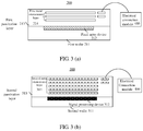
- FIG. 3 is a schematic cross-sectional diagram of a pixel array module 200 and a signal processing module 300 of an image sensor 20 according to an embodiment of the present application.
- FIG. 3 (a) is a schematic cross-sectional diagram of a pixel array module 200 of an embodiment of the present application
- FIG. 3 (b) is a schematic cross-sectional diagram of a signal processing module 300 of an embodiment of the present application.
- the pixel array module 200 is disposed on a first wafer 211, and includes a pixel array device 212, a first passivation layer 213, and a first metal interconnect layer 214 of a first predetermined number.
- the pixel array device 212 is an analog device, and the analog device is a device in an analog circuit for processing an analog signal, such as a resistor, a capacitor, an inductor, a diode, a transistor, a field effect transistor, an analog amplifier, etc.
- a supply voltage of the analog circuit may be 3.3V.
- the pixel array device 212 includes devices such as a photo diode (photo diode), a metal oxide semiconductor field effect transistor (metal oxide semiconductor field effect transistor, MOSFET), etc.
- the first metal interconnect layer 214 of the first predetermined number is used for interconnection between the pixel array devices 212 in the pixel array module 200.
- the first predetermined number is less than or equal to 4, and may generally be 2 or 3.
- the first metal interconnect layer 214 includes three metal interconnect layers. Multiple layers in the first metal interconnect layer 214 may be connected to the pixel array device 212.
- one or more layer of the first metal interconnect layer 214 may also be used to electrically connect with other modules in the image sensor 20, such as with the electrical connection module 400.
- the multiple layers of metals in the first metal interconnect layer 214 may be the same metal or different metals, and may be pure metals or alloys. For example, aluminum or copper.
- the first passivation layer 213 is used for isolating the pixel array device 212 from the first metal interconnect layer 214 and isolating the multiple layers of metals in the first metal interconnect layer 214 so as to prevent interference of electrical signals, and also for passivation of the metal layer in contact with the air in the first metal interconnect layer 214 so that a surface of the metal layer turns into a stable state.
- the first passivation layer 213 includes a plurality of passivation layers, which may be passivation layers of different materials, or may be passivation layers of the same material, for example, the first passivation layer 213 is a silicon nitride passivation layer.
- the first metal interconnect layer 214, the pixel array device 212, and the first passivation layer 213 form a pixel array circuit in the pixel array module 200.
- the signal processing module 300 is disposed on a second wafer 311, and includes a signal processing device 312, a second passivation layer 313, and a second metal interconnect layer 314 of a second predetermined number.
- the signal processing device 312 includes a digital device.
- the signal processing device 312 also includes an analog device.
- the digital device is a device in a digital circuit for processing digital signals, the digital circuit including various gate circuits, flip-flops, and various combinational logic circuits and sequential logic circuits composed of them.
- the supply voltage of the digital circuit may be 1.8V
- the signal processing device 312 includes: an analog to digital converter (analog to digital converter, ADC), a digital signal processor (digital signal processing, DSP), a memory (memory), and the like.
- ADC analog to digital converter
- DSP digital signal processing
- memory memory
- the pixel array device 212 is an analog device and the signal processing device 312 is a digital device, the requirements for device fabrication process of the two are different.
- the signal processing device 312 has more devices types than those of the pixel array device 212, and the spacing between devices is small with higher device performance requirements. Therefore, the fabrication process requirement of the signal processing device 312 is higher than that of the pixel array device 212, so that the cost of the signal processing device 312 is higher than that of the pixel array device 212.
- the second metal interconnect layer 314 of the second predetermined number is used for interconnection between the signal processing devices 312 in the signal processing module 300.
- the second predetermined number is greater than or equal to 4, and may generally be 5 or 6.
- the second metal interconnect layer 314 includes five metal interconnect layers. Multiple layers in the second metal interconnect layer 314 may be connected to the signal processing device 312.
- one or more layers of the second metal interconnect layer 314 may also be used to electrically connect with other modules in the image sensor, such as with the electrical connection module 400.
- the multiple layers of metals in the second metal interconnect layer 314 may be the same metal or different metals, and may be pure metals or alloys. For example, aluminum or copper.
- the second metal interconnect layer 314 is connected to the signal processing device 312, the first metal interconnect layer 214 is connected to the pixel array device 212, but the device spacing of the signal processing device 312 is smaller than that of the pixel array device 212, and the performance requirement of the signal processing device 312 is higher than that of the pixel array device 212. Therefore, the process requirements such as the line and space width of the second metal interconnect layer 314 are lower than those of the first metal interconnect layer 214, and the second metal interconnect layer 314 has more layers than those of the first metal interconnect layer 214, so that the cost of the second metal interconnect layer 314 is higher than that of the first metal interconnect layer 214.
- the second passivation layer 313 is used for isolating the signal processing device 312 from the second metal interconnect layer 314 and isolating the multiple layers of metals in the second metal interconnect layer 314, and also for passivation of the metal layer in contact with the air in the second metal interconnect layer 314.
- the second passivation layer 313 includes a plurality of passivation layers, which may be passivation layers of different materials, or may be passivation layers of the same material, for example, the second passivation layer 313 is a silicon nitride (Si 3 N 4 ) passivation layer.
- the second metal interconnect layer 314, the signal processing device 312, and the second passivation layer 313 form a signal processing circuit in the signal processing module 300.
- the pixel array module 200 and the signal processing module 300 are respectively disposed on different wafers. Therefore, the pixel array module 200 and the signal processing module 300 may be separately prepared, thereby performing process control on the two modules separately.
- the signal processing module 300 has more device types and more complicated circuit structures than those of the pixel array module 200, and the corresponding process requirement and mask cost are also higher.
- the high process requirement of the signal processing module 300 affects that of the pixel array module 200, so that the pixel array module 200 is also prepared by a high process requirement. This results in a waste of process cost for the pixel array module 200. Therefore, in the embodiment of the present application, the process requirement of separately preparing the pixel array module 200 and the reduction in the mask cost help to reduce the cost of the image sensor 20 as a whole.
- the pixel array module 200 and the signal processing module 300 may be two independent chips, which are respectively packaged in separate chips, or may be exposed chip modules grown on two wafers, and the two exposed chip modules are packaged to form one chip.
- the image sensor 20 may further include a plurality of other functional modules, which may be disposed on a plurality of wafers such as a third wafer, which is not limited in this embodiment.
- the electrical connection module 400 is any apparatus that implements electrical connection, and may be a wire bonding (wire bonding, WB) apparatus.
- the electrical connection module 400 may be a bonding wire (bonding wire) of Au (Au).
- the electrical connection may also be a micro metal connection post or other electrical connection manners such as a connector, as long as electrical connection between the two electrical modules may be achieved, which is not limited by the embodiment of the present application.
- the first wafer 211 and the second wafer 311 may be horizontally separated, that is, the first wafer 211 and the second wafer 311 are located on the same horizontal plane without overlapping with each other, and this connection process is of simple implementation and low cost.
- the first wafer 211 and the second wafer 311 may be disposed in stack, that is, the first wafer 211 and the second wafer 311 are stacked on top of each other.
- the first wafer 211 is disposed above the second wafer 311.
- a photosensitive circuit that is, the pixel array module 200
- a non-photosensitive circuit that is, the signal processing module 300
- the first wafer 211 and the second wafer 311 may be an epitaxial wafer (epitaxial wafer, Epi-wafer), that is, a single crystal material having a same lattice arrangement with the substrate, which is grown on a single crystal silicon (Si) substrate by an epitaxial process.
- the epitaxial layer may be a homoepitaxial layer of silicon (Si) or a heteroepitaxial layer of silicon germanium (SiGe) or silicon carbide (SiC). The performance of the epitaxial wafer is superior but the cost is high.
- the first wafer 211 and the second wafer 311 may also be a general standard wafer, that is, a silicon wafer that is produced not by an epitaxial process.
- the standard wafer costs less than the epitaxial wafer.
- the first wafer 211 is a low cost standard wafer.
- the pixel array module 200 is manufactured by using a simple and low-demand process, and the signal processing module 300 is manufactured by using a precise and high-demand process, where the cost per unit area of the pixel array module 200 is lower than that of the signal processing module 300.
- the cost per unit area of the pixel array module 200 is CA
- the area ratio of the pixel array module 200 and the signal processing module 300 in the image sensor the more cost reduction by adopting the apparatus and the method of separating the pixel array module 200 and the signal processing module 300 in the embodiment of the present application.
- the area ratio of the pixel array module 200 to the signal processing module 300 is greater than or equal to 7:3.
- the cost of connecting the pixel array module 200 and the connection module 230 of the signal processing module 300 is small compared with the cost of manufacturing the pixel array module 200.
- the cost of the connection module 230 is CC
- the wafer area of the image sensor 20 is S.
- the area of the pixel array module 200 is 0.7S and the cost per unit area thereof is CA
- the wafer area of the signal processing module 300 is 0.3S and the cost per unit area thereof is CB
- CB 1.5CA
- FIG. 4 is a schematic functional structural diagram of a pixel array module 200 and a signal processing module 300 according to an embodiment of the present application.
- FIG. 4 (a) is a schematic functional structural diagram of a pixel array module 200 of an embodiment of the present application
- FIG. 4 (b) is a schematic functional structural diagram of a signal processing module 300 of an embodiment of the present application.
- the pixel array module 200 includes a pixel array circuit 221 including a plurality of pixel sensitive units 222 configured to receive an optical signal and convert the optical signal into an electrical signal.
- the pixel sensitive unit 222 is a passive pixel sensitive unit composed of a photo diode and a field effect switch transistor.
- the pixel sensitive unit 222 is an active pixel sensitive unit composed of a photo diode, a field effect switch transistor and an amplifier.
- the photo diode in the pixel sensitive unit is configured to receive an optical signal and convert the optical signal into an electrical signal.
- a plurality of the pixel sensitive units 222 are arranged in M rows ⁇ N columns, where M, N are positive integers.
- the total number of pixels in the image sensor is M ⁇ N.
- the pixel array module 200 further includes: a row and column control circuit, where the row and column control circuit includes a row control circuit 223 and a column control circuit 224.
- the row control circuit 223 is connected to the pixel sensitive unit row in the pixel array circuit 221 for controlling and driving the pixel sensitive unit row in the pixel array circuit 221 so as to start conversion of the received optical signal.
- the row control circuit 223 is connected to the M-row pixel sensitive unit rows in the pixel array circuit 221 for controlling and driving each of the M rows of pixel sensitive unit row so as to start receiving and converting the optical signal.
- the row control circuit 223 is connected to a gate of the field effect switch transistor of each pixel sensitive unit 222 of the M rows of pixel sensitive unit row in the pixel array circuit 221, and the photo diode is driven to start receiving and converting the optical signal by switching on the field effect switching transistor.
- the row control circuit 223 includes a shift register.
- the row control circuit 223 includes a decoder.
- the row control circuit 223 is connected to the electrical connection module 400 for receiving a first control signal and driving the ith row of the pixel sensitive unit row in the M rows of pixel sensitive unit row with the action of the first control signal, where i is a positive integer and 1 ⁇ i ⁇ M.
- the first control signal is a timing control signal generated by another module in the image sensor, such as a logic control circuit in the signal processing module, and is transmitted to the row control circuit 223 through the electrical connection module 400.
- the column control circuit 224 is connected to the pixel sensitive unit column in the pixel array circuit 221 for driving the transmission of the electrical signal of the pixel sensitive unit column in the pixel array circuit 221.
- the column control circuit 224 is connected to the N columns of pixel sensitive unit column in the pixel array circuit 221 for driving the transmission of each column of electrical signals in the N columns of pixel sensitive unit column.
- the column control circuit 224 is connected to a gate of the field effect switch transistor of each pixel sensitive unit 222 of the N columns of pixel sensitive unit column in the pixel array circuit 221, and controls output of the electrical signal converted by the photo diode.
- the column control circuit 224 includes a shift register.
- the column control circuit 224 includes a decoder.
- the column control circuit 224 includes a multiplexer connected to the electrical connection module 400 for receiving a second control signal and selecting the j row of the pixel sensitive unit row in the N rows of pixel sensitive unit rows for the output of an electrical signal with the action of the second control signal, where j is a positive integer and 1 ⁇ j ⁇ M.
- the second control signal is a control signal generated by another module in the image sensor, such as a signal processing module, and is transmitted to the multiplexer of the column control circuit 224 through the electrical connection module 400.
- the pixel array module 200 further includes: a readout circuit 225 for receiving an electrical signal output with the control of the column control circuit 224 and transmitting the electrical signal through the electrical connection module 400 to the signal processing module 300.
- the readout circuit 225 includes an amplifying circuit 226 connected to the column control circuit 224 and the electrical connection module 400.
- the amplifying circuit 226 is configured to amplify the electrical signal output with the control of the column control circuit 224 and transmit the electrical signal to the signal processing module 300 through the electrical connection module 400.
- the amplifying circuit 226 is a programmable gain amplifier (programmable gain amplifier, PGA) circuit configured to receive a third control signal, amplify by different degrees the electrical signal output by the pixel array circuit 221 with the action of the third control signal, and transmit the electrical signal to the signal processing module 300, where the third control signal is a control signal generated by another module in the image sensor, such as the signal processing module, and is transmitted to the programmable gain amplifier through the electrical connection module 400.
- PGA programmable gain amplifier
- the signal processing module 300 includes an analog to digital converter (analog to digital converter, ADC) circuit 321 connected to the electrical connection module 400 for receiving an electrical signal generated by the pixel array module 200 and converting the electrical signal into a digital signal.
- ADC analog to digital converter
- the electrical signal is an analog electrical signal, which can be an analog voltage signal.
- the analog to digital conversion circuit samples, holds, quantizes, and encodes the analog voltage signal, and converts the analog voltage signal into a digital signal proportional thereto.
- the analog to digital conversion circuit 321 includes a parallel comparison ADC circuit, a successive approximation ADC circuit, a double integral ADC circuit, and the like.
- the parallel comparison ADC circuit includes a resistor divider, a voltage comparator, a register and an encoder.
- the parallel comparison ADC circuit has the advantage that the conversion time is short, which can be as short as several tens of nanoseconds, but more components are used. For example, an n-bit converter uses 2 n -1 comparators.
- the successive approximation ADC circuit includes a comparator, a ring divider, a control gate, a register, and a digital to analog converter, and the conversion time is about 1 microsecond.
- the double integral ADC circuit includes a comparator, a counter, an integrator and a logic control circuit.
- the advantage of the double integral ADC circuit is that the working performance is relatively stable and the anti-interference ability is strong, and the conversion time is about 1 to 2 milliseconds.
- the signal processing module 300 further includes: a digital signal processing circuit 322 connected to the analog to digital conversion circuit 321 for receiving a digital signal generated by the analog to digital conversion circuit 321 and processing the digital signal.
- the digital signal processing circuit 322 may include a digital signal processor (digital signal processor, DSP) or other programmable logic devices for processing a digital signal, discrete gate or transistor logic devices, and discrete hardware components.
- DSP digital signal processor
- the digital signal processing circuit can be used for signal processing such as digital filtering, adaptive filtering, fast Fourier transform, and the like. It can also be used for graphic image processing such as 2D and 3D graphics processing, image compression and transmission, image enhancement, and data encryption.
- the signal processing module 300 further includes: a storage circuit 323 connected to the digital processing circuit 322 for storing a particular signal, the particular signal including a signal processed by the digital processing circuit 322 which can be an image signal.
- the storage circuit 323 may include: a random access memory (random access memory, RAM) and a non-volatile memory (non-volatile memory, NVM).
- the RAM is, for example, a static random access memory (static SRAM)
- the NVM is, for example, a flash memory FLASH. It should be noted that the memories in the embodiments of the present application aim to include but are not limited to these memories and any memory of another proper type.
- the signal processing module 300 further includes: a logic control circuit 324 connected to the analog to digital conversion circuit 321, the digital processing circuit 322, the storage circuit 323, and the electrical connection module 400.
- the logic control circuit 324 is configured to generate a control signal and to transmit the control signal to the analog to digital conversion circuit 321, the digital processing circuit 322, the storage circuit 323, and the electrical connection module 400.
- the logic control circuit 324 may include a micro controller unit (micro controller unit, MCU) or a central processing unit (central processing unit, CPU) and the like.
- MCU micro controller unit
- CPU central processing unit
- the logic control circuit 324 is a main control circuit of the image sensor 20, coordinates the operation of other parts of the circuit, and provides control signals such as timing control signals for the row control circuit 223, the column control circuit 224, the readout circuit 225, the analog to digital conversion circuit 321, the digital processing circuit 322, and the storage circuit 323.
- the logic control circuit also controls the row control circuit 223 for driving the pixel sensitive unit row in the pixel array circuit 221, and controls the column control circuit 224 for controlling and outputting the electrical signal of the pixel sensitive unit column in the pixel array circuit 221, controls the readout circuit 225 for amplifying an electrical signal by different degrees, and controls the analog to digital conversion circuit 321 for converting the electrical signal into a digital signal, and controls the digital processing circuit 322 and the storage circuit 323 for processing the digital signal and store the processed image signal.
- the logic control circuit 324 is connected to the electrical connection module 400, and transmits a control signal to the row control circuit 223, the column control circuit 224, and the readout circuit 225 in the pixel array module through the electrical connection module 400.
- the signal processing module 300 further includes: a clock circuit 325 connected to the analog to the digital conversion circuit 321, the digital processing circuit 322, and the storage circuit 323, and is configured to provide a unified reference clock source for each circuit in the signal processing module 300 so that the circuit timing of each part is uniform.
- the clock circuit 325 may include a phase locked loop (phase locked loop, PLL) circuit, an on chip oscillator (on chip oscillator, OSC), and the like.
- PLL phase locked loop
- OSC on chip oscillator
- FIG. 5 illustrates a schematic connection diagram of an image sensor 20 according to an embodiment of the present application.
- an electrical connection module 400 includes a first electrical connection module 410 and a second electrical connection module 420.
- a logic control circuit in a signal processing module 300 is connected to a row control circuit 223, a column control circuit 224, and a readout circuit 225 in a pixel array module 200 through the first electrical connection module 410.
- the readout circuit 225 in the pixel array module 200 is connected to an analog to digital conversion circuit 321 in the signal processing module 300 through the second electrical connection module 420.
- the analog to digital conversion circuit 321 is connected to an amplifying circuit 226 in the readout circuit 225 through the second electrical connection module 420.
- the first electrical connection module 410 is configured to transmit a control signal generated by the logic control circuit 324 to the row control circuit 223, the column control circuit 224, and the readout circuit 225.
- the second electrical connection module 420 is configured to transmit an electrical signal output by the readout circuit 225 to the analog to digital conversion circuit 321.
- the first electrical connection module 410 and the second electrical connection module 420 can also transmit other signals generated by the other pixel array module 200 and the signal processing module 300.
- signal transmission between the pixel array module 200 and the signal processing module 300 can be completed through the first electrical connection module 410 and the second electrical connection module 420, with a small signal type, and the implementation between the first electrical connection module 410 and the second electrical connection module 420 is simple.
- FIG. 6 illustrates a schematic flowchart of a method 600 for manufacturing an image sensor according to an embodiment of the present application.
- the image sensor of the foregoing embodiments of the present application can be manufactured with this method 600.
- devices in the pixel array module consist of analog devices.
- the pixel array module includes a first metal interconnect layer of a first predetermined number, the devices in the pixel array module are interconnected through the first metal interconnect layer, and the first predetermined number is less than or equal to 4.
- the first predetermined number is 3.
- the pixel array module includes a pixel array circuit including a plurality of pixel sensitive units.
- the pixel array module includes a row control circuit and a column control circuit, where the row control circuit is connected to a pixel sensitive unit row in the pixel array circuit through the first metal interconnect layer, and the column control circuit is connected to a pixel sensitive unit column in the pixel array circuit through the first metal interconnect layer.
- the pixel array module further includes a readout circuit connected to the column control circuit through the first metal interconnect layer.
- the readout circuit includes an amplifying circuit connected to the column control circuit through the first metal interconnect layer.
- S620 preparing a signal processing module on a second wafer.
- devices in the pixel array module consist of analog devices.
- the signal processing module includes a second metal interconnect layer of a second predetermined number, the devices in the signal processing module are interconnected through the second metal interconnect layer, and the second predetermined number is greater than or equal to 4.
- the second predetermined number is 5.
- the signal processing module includes an analog to digital conversion circuit connected to the electrical connection module through the second metal interconnect layer.
- the signal processing module further includes a digital processing circuit.
- the signal processing module further includes a logic control circuit connected to the analog to digital conversion circuit, the digital processing circuit, and the storage circuit through the second metal interconnect layer.
- the signal processing module further includes a storage circuit configured to be connected to the digital processing circuit through the second metal interconnect layer.
- the pixel array module is connected to the electrical connection module through the first metal interconnect layer.
- a row control circuit, a column control circuit, and a readout circuit in the pixel array module are connected to the electrical connection module through the first metal interconnect layer.
- the signal processing module is connected to the electrical connection module through the second metal interconnect layer.
- a logic control circuit and an analog to digital conversion circuit in the signal processing module are connected to the electrical connection module through the second metal interconnect layer.
- the analog to digital conversion circuit in the signal processing module is connected to the readout circuit in the pixel array module through the electrical connection module.
- the logic control circuit in the signal processing module is connected to the row control circuit, the column control circuit, and the readout circuit in the pixel array module through the electrical connection module.
- the electrical connection module includes a wire bonding apparatus.
- the first wafer and the second wafer are epitaxial wafers or standard wafers.
- the first wafer and the second wafer are disposed in stack.
- the embodiment of the present application also provides an electronic device 30, which may include an image sensor 310, and the image sensor 310 may be the image sensor 20 in the foregoing apparatus embodiment.
- the image sensor 30 can be obtained using the method described in FIG. 6 , which will not be repeatedly described here for brevity.
- the disclosed system, apparatus, and method may be implemented in another manner.
- the described apparatus embodiment is merely an example.
- the unit division is merely logical function division and may be other division in actual implementation.
- a plurality of units or components may be combined or integrated into another system, or some features may be ignored or not performed.
- the displayed or discussed mutual couplings or direct couplings or communication connections may be implemented by using some interfaces.
- the indirect couplings or communication connections between the apparatuses or units may be implemented in electrical, mechanical, or other forms.
- the units described as separate components may or may not be physically separate, and components displayed as units may or may not be physical units, may be located in one position, or may be distributed on multiple network units. Some or all of the units may be selected according to actual requirements to achieve the objectives of the solutions of the embodiments.
Landscapes
- Engineering & Computer Science (AREA)
- Multimedia (AREA)
- Signal Processing (AREA)
- Solid State Image Pick-Up Elements (AREA)
Abstract
Description
- The present application relate to the field of image sensor, and in particular, to an image sensor, a manufacturing method thereof and an electronic device.
- With the development of semiconductor and integrated circuit technology, the device types of chips are becoming more and more abundant, with more process requirements and a greater number of process layers, so the cost of chips is getting higher and higher. Since the overall chip cost is affected by the device type and process complexity of each part of the chip, the cost per unit area of the chip is determined by the portion corresponding to the highest cost per unit area.
- In an image sensor (image sensor) chip, a pixel array (pixel array) unit and a signal processing unit are included, where the pixel array unit occupies most of the area of the chip, while the signal processing unit occupies a small area. Generally, the pixel array unit has a small device type and a low process requirement, and thus the cost per unit area corresponding to the pixel array unit is relatively low. While the signal processing unit includes a variety of device types, which requires a more complicated process, and thus the cost per unit area corresponding to the signal processing unit is relatively high. In the existing image sensor chip, the cost per unit area of the chip is generally determined by the cost per unit area of the signal processing unit, and the total cost of the chip is high.
- Embodiments of the present application provide an image sensor and a manufacturing method thereof, and an electronic device, which is capable of reducing the cost of the image sensor.
- In a first aspect, an image sensor is provided, including: a pixel array module disposed on a first wafer; a signal processing module disposed on a second wafer; an electrical connection module connecting the pixel array module and the signal processing module; where the pixel array module is configured to receive an optical signal and convert the optical signal into an electrical signal, and the signal processing module is configured to process the electrical signal.
- In the technical solution of the embodiment of the present application, devices of the image sensor are disposed on two wafers, and the connection is realized by electrical connection between the two wafers, which can reduce the cost of the image sensor.
- In one possible implementation manner, devices in the pixel array module consist of analog devices, and devices in the signal processing module includes digital devices.
- The pixel array module consisting of analog devices is disposed on a single wafer, which may reduce the cost of the module.
- In one possible implementation manner, the pixel array module includes a first metal interconnect layer of a first predetermined number, the first metal interconnect layer is configured for interconnection of the devices in the pixel array module, and the first predetermined number is less than or equal to 4.
- In one possible implementation manner, the first metal interconnect layer is connected to the electrical connection module.
- In one possible implementation manner, the signal processing module includes a second metal interconnect layer of a first predetermined number, the second metal interconnect layer is configured for interconnection of the devices in the signal processing module, and the second predetermined number is greater than or equal to 4.
- In one possible implementation manner, the second metal interconnect layer is connected to the electrical connection module.
- In one possible implementation manner, the pixel array module includes a pixel array circuit including a plurality of pixel sensitive units configured to receive the optical signal and convert the optical signal into the electrical signal.
- In one possible implementation manner, the pixel array module further includes a row and column control circuit configured to receive a control signal generated by the signal processing module, and to control the plurality of pixel sensitive units for receiving the optical signal and converting the optical signal to the electrical signal.
- In one possible implementation manner, the pixel array module further includes a readout circuit configured to receive the electrical signal output by the plurality of pixel sensitive units and send the electrical signal to the signal processing module.
- In one possible implementation manner, the readout circuit includes an amplifying circuit configured to amplify the electrical signal output by the plurality of pixel sensitive units.
- In one possible implementation manner, the signal processing module includes an analog to digital conversion circuit configured to receive the electrical signal generated by the pixel array module and convert the electrical signal into a digital electrical signal.
- In one possible implementation manner, the signal processing module further includes a digital processing circuit configured to receive the digital electrical signal generated by the analog to digital conversion circuit and process the digital electrical signal.
- In one possible implementation manner, the signal processing module further includes a logic control circuit configured to generate a control signal.
- In one possible implementation manner, the signal processing module further includes a storage circuit configured to store a particular signal, where the particular signal includes a signal processed by the digital processing circuit.
- In one possible implementation manner, the analog to digital conversion circuit is connected to the amplifying circuit through the electrical connection module, and the logic control circuit is connected to the row and column control circuit and the readout circuit through the electrical connection module.
- That is to say, the electrical connection module between the two wafers is disposed between the analog to digital conversion circuit and the amplifying circuit, and between the logic control circuit and the row and column control circuit and the readout circuit. With this arrangement, the implementation complexity of the electrical connection module between the two wafers can be reduced.
- In one possible implementation manner, the electrical connection module is configured to transmit the electrical signal generated by the pixel array module and a control signal generated by the signal processing module.
- In one possible implementation manner, the electrical connection module includes a wire bonding apparatus.
- In one possible implementation manner, the first wafer and the second wafer are epitaxial wafers or standard wafers.
- In one possible implementation manner, the first wafer and the second wafer are disposed in stack.
- In a second aspect, a manufacturing method of an image sensor is provided, including:
- preparing a pixel array module on a first wafer;
- preparing a signal processing module on a second wafer; and
- connecting the pixel array module and the signal processing module by preparing an electrical connection module.
- In one possible implementation manner, devices in the pixel array module consist of analog devices, and devices in the signal processing module include digital devices.
- In one possible implementation manner, the pixel array module includes a first metal interconnect layer of a first predetermined number, the devices in the pixel array module are interconnected through the first metal interconnect layer, and the first predetermined number is less than or equal to 4.
- In one possible implementation manner, the pixel array module is connected to the electrical connection module through the first metal interconnect layer.
- In one possible implementation manner, the pixel array module includes a pixel array circuit including a plurality of pixel sensitive units.
- In one possible implementation manner, the pixel array module includes a row control circuit and a column control circuit, where the row control circuit is connected to a pixel sensitive unit row in the pixel array circuit through the first metal interconnect layer, and the column control circuit is connected to a pixel sensitive unit column in the pixel array circuit through the first metal interconnect layer.
- In one possible implementation manner, the row control circuit and the column control circuit are connected to the electrical connection module through the first metal interconnect layer.
- In one possible implementation manner, the pixel array module further includes a readout circuit connected to the column control circuit and the electrical connection module through the first metal interconnect layer.
- In one possible implementation manner, the readout circuit includes an amplifying circuit connected to the column control circuit and the electrical connection module through the first metal interconnect layer.
- In one possible implementation manner, the signal processing module includes a second metal interconnect layer of a second predetermined number, the devices in the signal processing module are interconnected through the second metal interconnect layer, and the second predetermined number is greater than or equal to 4.
- In one possible implementation manner, the signal processing module is connected to the electrical connection module through the second metal interconnect layer.
- In one possible implementation manner, the signal processing module includes an analog to digital conversion circuit connected to the electrical connection module through the second metal interconnect layer.
- In one possible implementation manner, the signal processing module further includes a digital processing circuit connected to the analog to digital conversion circuit through the second metal interconnect layer.
- In one possible implementation manner, the signal processing module further includes a logic control circuit connected to the analog to digital conversion circuit, the digital processing circuit, the storage circuit, and the electrical connection module through the second metal interconnect layer.
- In one possible implementation manner, the signal processing module further includes a storage circuit configured to be connected to the digital processing circuit through the second metal interconnect layer.
- In one possible implementation manner, the analog to digital conversion signal is connected to the readout circuit through the electrical connection module, and the logic control circuit is connected to the row control circuit, the column control circuit, and the readout circuit through the electrical connection module.
- In one possible implementation, the electrical connection module includes a wire bonding apparatus.
- In one possible implementation manner, the first wafer and the second wafer are epitaxial wafers or standard wafers.
- In one possible implementation manner, the first wafer and the second wafer are disposed in stack.
- In a third aspect, an electronic device is provided, including: the image sensor of the first aspect or any one of its implementation manners.
-
-
FIG. 1 is a schematic diagram of an image sensor according to an embodiment of the present application. -
FIG. 2 is a schematic structural diagram of an image sensor according to another embodiment of the present application. -
FIG. 3 (a) is a schematic cross-sectional diagram of a pixel array module of an image sensor according to an embodiment of the present application. -
FIG. 3 (b) is a schematic cross-sectional diagram of a signal processing module of an image sensor according to an embodiment of the present application. -
FIG. 4 (a) is a schematic functional structural diagram of a pixel array module of an image sensor according to an embodiment of the present application. -
FIG. 4 (b) is a schematic functional structural diagram of a signal processing module of an image sensor according to an embodiment of the present application. -
FIG. 5 is a schematic connection diagram of an image sensor according to an embodiment of the present application. -
FIG. 6 is a schematic flowchart of a manufacturing method of an image sensor according to an embodiment of the present application. -
FIG. 7 is a schematic block diagram of an electronic device according to an embodiment of the present application. - The technical solutions in embodiments of the present application will be described hereinafter in conjunction with the accompanying drawings.
- It should be understood that specific examples in embodiments of the present application are just for helping those skilled in the art better understand the embodiments of the present application, rather than for limiting the scope of the present application.
- It should be further understood that, in various embodiments of the present application, the sequence number of each process does not mean the order of execution, and the order of execution of each process should be determined by its function and internal logic, and should not set any limitation to the implementation process of the embodiments of the present application.
- It should be understood that the various embodiments described in the present specification may be implemented separately or in combination, which is not limited by the embodiments of the present application.
- The technical solutions of the embodiments of the present application can be applied to various image sensors, such as a biometric image sensor, which is not limited by the embodiments of the present application.
- As a common application scenario, the image sensor provided in embodiments of the present application may be applied to a smart phone, a camera, a tablet computer and another mobile terminal having an imaging function or another terminal device.
-
FIG. 1 shows a schematic diagram of an example of a complementary metal oxide semiconductor (complementary metal oxide semiconductor, CMOS)image sensor 10. As shown inFIG. 1 , theCMOS image sensor 10 is a CMOS image sensor chip, including: aCMOS pixel array 110, an analog todigital conversion circuit 120, asignal processing circuit 130, adigital processing circuit 140, and alogic control circuit 150. TheCMOS pixel array 110 receives an optical signal and converts the optical signal into an electrical signal and transmits the electrical signal to thesignal processing circuit 130 and the analog todigital conversion circuit 120. After being processed by the analog todigital conversion circuit 120, a digital signal is obtained, and the digital signal is transmitted to thedigital processing circuit 140 for digital signal processing to obtain an image signal. Thelogic control circuit 150 provides timing and other various control signals for theCMOS pixel array 110, the analog todigital conversion circuit 120, thesignal processing circuit 130, and thedigital processing circuit 140. - In the
CMOS image sensor 10, the total number of pixels of theCMOS pixel array 110 is one of the main technical indicators for measuring the CMOS image sensor, and determines various factors such as the photographic performance, resolution, and the like of the CMOS image sensor. Thus, theCMOS pixel array 110 occupies a large portion of the chip area, generally more than 70% of the total chip area. In theCMOS pixel array 110, an array consists of a plurality of pixel sensitive units is mainly included, and each of the pixel sensitive units consists of one photo diode and one or more CMOS switching transistors, so that the CMOS pixel array has a small device type, the circuit structure is relatively simple, and the device process requirements are relatively low. - In the
CMOS image sensor 10, except for theCMOS pixel array 110, other functional circuits occupy a relatively small portion of the chip area, typically less than 30% of the total chip area. But among these functional circuits, such as thedigital processing circuit 140, the circuit structure is relatively complex with a great many of device types and high integration due to the need for implementing more complex functions, and therefore the process requirements are relatively high. - In the semiconductor integrated circuit process, the manufacturing cost of the chip includes the cost of the wafer, the test, the package, and the mask. The cost of the mask is the cost required to manufacture the chip by using different process technologies, and it is greatly increased for those circuit with high integration and high requirements on device process. Since the overall process requirement of the chip is determined by the circuit unit having the highest process requirement in the chip, the mask cost per chip area of the chip is the mask cost per unit area of the circuit unit having the highest process requirement.
- For example, if the area of the
CMOS image sensor 10 is S, where the circuit with the highest process requirement is thedigital processing circuit 140, and the cost per unit area of thedigital processing circuit 140 is CB, then the cost of the entireCMOS image sensor 10 is CB∗S. Thedigital processing circuit 140 only occupies a small chip area in the entireCMOS image sensor 10; however due to the high process requirements for thedigital processing circuit 140, the process cost of the chip is greatly increased, resulting in waste of cost. - Hereinafter, an image sensor according to an embodiment of the present application will be described in detail with reference to
FIGS. 2 to 5 . - It should be noted that in the embodiments illustrated below, the same structure is denoted by the same reference numeral for ease of understanding, and detailed description of the same structure is omitted for brevity.
-
FIG. 2 is a schematic structural diagram of animage sensor 20 according to an embodiment of the present application. As shown inFIG. 2 , theimage sensor 20 includes apixel array module 200, asignal processing module 300, and anelectrical connection module 400. Thepixel array module 200 is disposed on afirst wafer 211, thesignal processing module 300 is disposed on asecond wafer 311, and theelectrical connection module 400 connects thepixel array module 200 and thesignal processing module 300. Thepixel array module 200 is configured to receive an optical signal and convert the optical signal into an electrical signal, and thesignal processing module 300 is configured to process the electrical signal. In the embodiment of the present application, thepixel array module 200 may include theCMOS pixel array 110 ofFIG. 1 , and thesignal processing module 300 may include the analog todigital conversion circuit 120, thesignal processing circuit 130, thedigital processing circuit 140, and thelogic control circuit 150 inFIG. 1 . - Optionally, the
image sensor 20 is a complementary metal oxide semiconductor image sensor (CMOS image sensor, CIS), such as a CMOS passive pixel sensor (passive pixel sensor, CMOS-PPS), a CMOS active pixel sensor (active pixel sensor, CMOS-APS), and a CMOS digital pixel sensor (digital pixel sensor, CMOS-DPS). Correspondingly, thepixel array module 200 includes a pixel sensitive unit array, where the pixel sensitive unit column can be a passive pixel (passive pixel) sensitive unit or an active pixel (active pixel) sensitive unit. - Optionally, the
image sensor 20 is a charge coupled device (charge coupled device, CCD) image sensor. Correspondingly, thepixel array module 200 includes a metal oxide semiconductor (metal oxide semiconductor, MOS) photosensitive element array, where one MOS photosensitive element array is a MOS capacitor. -
FIG. 3 is a schematic cross-sectional diagram of apixel array module 200 and asignal processing module 300 of animage sensor 20 according to an embodiment of the present application.FIG. 3 (a) is a schematic cross-sectional diagram of apixel array module 200 of an embodiment of the present application, andFIG. 3 (b) is a schematic cross-sectional diagram of asignal processing module 300 of an embodiment of the present application. - As shown in
FIG. 3 (a) , thepixel array module 200 is disposed on afirst wafer 211, and includes apixel array device 212, afirst passivation layer 213, and a firstmetal interconnect layer 214 of a first predetermined number. - The
pixel array device 212 is an analog device, and the analog device is a device in an analog circuit for processing an analog signal, such as a resistor, a capacitor, an inductor, a diode, a transistor, a field effect transistor, an analog amplifier, etc. In the embodiment of the present application, a supply voltage of the analog circuit may be 3.3V. - Specifically, the
pixel array device 212 includes devices such as a photo diode (photo diode), a metal oxide semiconductor field effect transistor (metal oxide semiconductor field effect transistor, MOSFET), etc. - The first
metal interconnect layer 214 of the first predetermined number is used for interconnection between thepixel array devices 212 in thepixel array module 200. - Optionally, the first predetermined number is less than or equal to 4, and may generally be 2 or 3. For example, as shown in
FIG. 3 (a) , the firstmetal interconnect layer 214 includes three metal interconnect layers. Multiple layers in the firstmetal interconnect layer 214 may be connected to thepixel array device 212. - Optionally, one or more layer of the first
metal interconnect layer 214 may also be used to electrically connect with other modules in theimage sensor 20, such as with theelectrical connection module 400. - Optionally, the multiple layers of metals in the first
metal interconnect layer 214 may be the same metal or different metals, and may be pure metals or alloys. For example, aluminum or copper. - The
first passivation layer 213 is used for isolating thepixel array device 212 from the firstmetal interconnect layer 214 and isolating the multiple layers of metals in the firstmetal interconnect layer 214 so as to prevent interference of electrical signals, and also for passivation of the metal layer in contact with the air in the firstmetal interconnect layer 214 so that a surface of the metal layer turns into a stable state. - Optionally, the
first passivation layer 213 includes a plurality of passivation layers, which may be passivation layers of different materials, or may be passivation layers of the same material, for example, thefirst passivation layer 213 is a silicon nitride passivation layer. - In the embodiment of the present application, the first
metal interconnect layer 214, thepixel array device 212, and thefirst passivation layer 213 form a pixel array circuit in thepixel array module 200. - As shown in
FIG. 3 (b) , thesignal processing module 300 is disposed on asecond wafer 311, and includes asignal processing device 312, asecond passivation layer 313, and a secondmetal interconnect layer 314 of a second predetermined number. - The
signal processing device 312 includes a digital device. Optionally, thesignal processing device 312 also includes an analog device. The digital device is a device in a digital circuit for processing digital signals, the digital circuit including various gate circuits, flip-flops, and various combinational logic circuits and sequential logic circuits composed of them. In the embodiment of the present application, the supply voltage of the digital circuit may be 1.8V - Specifically, the
signal processing device 312 includes: an analog to digital converter (analog to digital converter, ADC), a digital signal processor (digital signal processing, DSP), a memory (memory), and the like. - Since the
pixel array device 212 is an analog device and thesignal processing device 312 is a digital device, the requirements for device fabrication process of the two are different. In the embodiment of the present application, thesignal processing device 312 has more devices types than those of thepixel array device 212, and the spacing between devices is small with higher device performance requirements. Therefore, the fabrication process requirement of thesignal processing device 312 is higher than that of thepixel array device 212, so that the cost of thesignal processing device 312 is higher than that of thepixel array device 212. - The second
metal interconnect layer 314 of the second predetermined number is used for interconnection between thesignal processing devices 312 in thesignal processing module 300. - Optionally, the second predetermined number is greater than or equal to 4, and may generally be 5 or 6. For example, as shown in
FIG. 3 (b) , the secondmetal interconnect layer 314 includes five metal interconnect layers. Multiple layers in the secondmetal interconnect layer 314 may be connected to thesignal processing device 312. - Optionally, one or more layers of the second
metal interconnect layer 314 may also be used to electrically connect with other modules in the image sensor, such as with theelectrical connection module 400. - Optionally, the multiple layers of metals in the second
metal interconnect layer 314 may be the same metal or different metals, and may be pure metals or alloys. For example, aluminum or copper. - The second
metal interconnect layer 314 is connected to thesignal processing device 312, the firstmetal interconnect layer 214 is connected to thepixel array device 212, but the device spacing of thesignal processing device 312 is smaller than that of thepixel array device 212, and the performance requirement of thesignal processing device 312 is higher than that of thepixel array device 212. Therefore, the process requirements such as the line and space width of the secondmetal interconnect layer 314 are lower than those of the firstmetal interconnect layer 214, and the secondmetal interconnect layer 314 has more layers than those of the firstmetal interconnect layer 214, so that the cost of the secondmetal interconnect layer 314 is higher than that of the firstmetal interconnect layer 214. - The
second passivation layer 313 is used for isolating thesignal processing device 312 from the secondmetal interconnect layer 314 and isolating the multiple layers of metals in the secondmetal interconnect layer 314, and also for passivation of the metal layer in contact with the air in the secondmetal interconnect layer 314. - Optionally, the
second passivation layer 313 includes a plurality of passivation layers, which may be passivation layers of different materials, or may be passivation layers of the same material, for example, thesecond passivation layer 313 is a silicon nitride (Si3N4) passivation layer. - In the embodiment of the present application, the second
metal interconnect layer 314, thesignal processing device 312, and thesecond passivation layer 313 form a signal processing circuit in thesignal processing module 300. - The
pixel array module 200 and thesignal processing module 300 are respectively disposed on different wafers. Therefore, thepixel array module 200 and thesignal processing module 300 may be separately prepared, thereby performing process control on the two modules separately. Thesignal processing module 300 has more device types and more complicated circuit structures than those of thepixel array module 200, and the corresponding process requirement and mask cost are also higher. When thepixel array module 200 and thesignal processing module 300 are fabricated together on a same wafer, the high process requirement of thesignal processing module 300 affects that of thepixel array module 200, so that thepixel array module 200 is also prepared by a high process requirement. This results in a waste of process cost for thepixel array module 200. Therefore, in the embodiment of the present application, the process requirement of separately preparing thepixel array module 200 and the reduction in the mask cost help to reduce the cost of theimage sensor 20 as a whole. - It should be understood that the
pixel array module 200 and thesignal processing module 300 may be two independent chips, which are respectively packaged in separate chips, or may be exposed chip modules grown on two wafers, and the two exposed chip modules are packaged to form one chip. - It should be understood that the
image sensor 20 may further include a plurality of other functional modules, which may be disposed on a plurality of wafers such as a third wafer, which is not limited in this embodiment. - Optionally, the
electrical connection module 400 is any apparatus that implements electrical connection, and may be a wire bonding (wire bonding, WB) apparatus. For example, theelectrical connection module 400 may be a bonding wire (bonding wire) of Au (Au). - It should be understood that the electrical connection may also be a micro metal connection post or other electrical connection manners such as a connector, as long as electrical connection between the two electrical modules may be achieved, which is not limited by the embodiment of the present application.
- Optionally, the
first wafer 211 and thesecond wafer 311 may be horizontally separated, that is, thefirst wafer 211 and thesecond wafer 311 are located on the same horizontal plane without overlapping with each other, and this connection process is of simple implementation and low cost. - Optionally, the
first wafer 211 and thesecond wafer 311 may be disposed in stack, that is, thefirst wafer 211 and thesecond wafer 311 are stacked on top of each other. Preferably, thefirst wafer 211 is disposed above thesecond wafer 311. In this manner a photosensitive circuit, that is, thepixel array module 200, is disposed above a non-photosensitive circuit, that is, thesignal processing module 300, so that the area ratio of thepixel array module 200 in theimage sensor 20 can be enlarged, that is, the photosensitive area of theimage sensor 20 can be enlarged. - Optionally, the
first wafer 211 and thesecond wafer 311 may be an epitaxial wafer (epitaxial wafer, Epi-wafer), that is, a single crystal material having a same lattice arrangement with the substrate, which is grown on a single crystal silicon (Si) substrate by an epitaxial process. The epitaxial layer may be a homoepitaxial layer of silicon (Si) or a heteroepitaxial layer of silicon germanium (SiGe) or silicon carbide (SiC). The performance of the epitaxial wafer is superior but the cost is high. - Optionally, the
first wafer 211 and thesecond wafer 311 may also be a general standard wafer, that is, a silicon wafer that is produced not by an epitaxial process. The standard wafer costs less than the epitaxial wafer. Preferably, thefirst wafer 211 is a low cost standard wafer. - In the solution of the embodiment of the present application, the
pixel array module 200 is manufactured by using a simple and low-demand process, and thesignal processing module 300 is manufactured by using a precise and high-demand process, where the cost per unit area of thepixel array module 200 is lower than that of thesignal processing module 300. For example, in the embodiment of the present application, the cost per unit area of thepixel array module 200 is CA, and that of thesignal processing module 300 is CB, CB=1.5CA∼2CA. - The larger the area ratio of the
pixel array module 200 and thesignal processing module 300 in the image sensor, the more cost reduction by adopting the apparatus and the method of separating thepixel array module 200 and thesignal processing module 300 in the embodiment of the present application. For example, in the embodiment of the present application, the area ratio of thepixel array module 200 to thesignal processing module 300 is greater than or equal to 7:3. - With the method in the embodiment of the present application, in which the
pixel array module 200 and thesignal processing module 300 are separated, the cost of connecting thepixel array module 200 and the connection module 230 of thesignal processing module 300 is small compared with the cost of manufacturing thepixel array module 200. For example, in the embodiment of the present application, the cost of the connection module 230 is CC, and the area of thepixel array module 200 is 0.7S, where S is the wafer area of theimage sensor 20, and CC=0.05CA∗S. - If the
pixel array module 200 and thesignal processing module 300 are on the same wafer, the wafer area of theimage sensor 20 is S. The area of thepixel array module 200 is 0.7S and the cost per unit area thereof is CA, the wafer area of thesignal processing module 300 is 0.3S and the cost per unit area thereof is CB, and CB=1.5CA, and then the cost of theimage sensor 20 is P1=CB∗S = 1.5 CA ∗ S. - As shown in
FIG. 2 , in the embodiment of the present application, thepixel array module 200 and thesignal processing module 300 are connected through the connection module 230. The cost of the connection module 230 is CC=0.05CA∗S, and then the cost of theimage sensor 20 is P2=CA∗0.7S+CB∗0.3S+CC=1.2CA∗S. - Therefore, in the embodiment of the present application, the cost saved by the
image sensor 20 is ΔP=P1-P2=0.3CA∗S, that is, the cost is reduced by 20% compared with the case where thepixel array module 200 and thesignal processing module 300 are on the same wafer. -
FIG. 4 is a schematic functional structural diagram of apixel array module 200 and asignal processing module 300 according to an embodiment of the present application.FIG. 4 (a) is a schematic functional structural diagram of apixel array module 200 of an embodiment of the present application, andFIG. 4 (b) is a schematic functional structural diagram of asignal processing module 300 of an embodiment of the present application. - As shown in
FIG. 4 (a) , thepixel array module 200 includes apixel array circuit 221 including a plurality of pixelsensitive units 222 configured to receive an optical signal and convert the optical signal into an electrical signal. - Optionally, the pixel
sensitive unit 222 is a passive pixel sensitive unit composed of a photo diode and a field effect switch transistor. - Optionally, the pixel
sensitive unit 222 is an active pixel sensitive unit composed of a photo diode, a field effect switch transistor and an amplifier. - Specifically, the photo diode in the pixel sensitive unit is configured to receive an optical signal and convert the optical signal into an electrical signal.
- Optionally, a plurality of the pixel
sensitive units 222 are arranged in M rows × N columns, where M, N are positive integers. The total number of pixels in the image sensor is M × N. - Optionally, as shown in
FIG. 4 (a) , thepixel array module 200 further includes: a row and column control circuit, where the row and column control circuit includes arow control circuit 223 and acolumn control circuit 224. Therow control circuit 223 is connected to the pixel sensitive unit row in thepixel array circuit 221 for controlling and driving the pixel sensitive unit row in thepixel array circuit 221 so as to start conversion of the received optical signal. For example, therow control circuit 223 is connected to the M-row pixel sensitive unit rows in thepixel array circuit 221 for controlling and driving each of the M rows of pixel sensitive unit row so as to start receiving and converting the optical signal. Specifically, therow control circuit 223 is connected to a gate of the field effect switch transistor of each pixelsensitive unit 222 of the M rows of pixel sensitive unit row in thepixel array circuit 221, and the photo diode is driven to start receiving and converting the optical signal by switching on the field effect switching transistor. - Optionally, the
row control circuit 223 includes a shift register. - Optionally, the
row control circuit 223 includes a decoder. - Optionally, the
row control circuit 223 is connected to theelectrical connection module 400 for receiving a first control signal and driving the ith row of the pixel sensitive unit row in the M rows of pixel sensitive unit row with the action of the first control signal, where i is a positive integer and 1 ≤ i ≤ M. The first control signal is a timing control signal generated by another module in the image sensor, such as a logic control circuit in the signal processing module, and is transmitted to therow control circuit 223 through theelectrical connection module 400. - Optionally, as shown in
FIG. 4(a) , thecolumn control circuit 224 is connected to the pixel sensitive unit column in thepixel array circuit 221 for driving the transmission of the electrical signal of the pixel sensitive unit column in thepixel array circuit 221. For example, thecolumn control circuit 224 is connected to the N columns of pixel sensitive unit column in thepixel array circuit 221 for driving the transmission of each column of electrical signals in the N columns of pixel sensitive unit column. Specifically, thecolumn control circuit 224 is connected to a gate of the field effect switch transistor of each pixelsensitive unit 222 of the N columns of pixel sensitive unit column in thepixel array circuit 221, and controls output of the electrical signal converted by the photo diode. - Optionally, the
column control circuit 224 includes a shift register. - Optionally, the
column control circuit 224 includes a decoder. - Optionally, the
column control circuit 224 includes a multiplexer connected to theelectrical connection module 400 for receiving a second control signal and selecting the j row of the pixel sensitive unit row in the N rows of pixel sensitive unit rows for the output of an electrical signal with the action of the second control signal, where j is a positive integer and 1 ≤ j ≤ M. The second control signal is a control signal generated by another module in the image sensor, such as a signal processing module, and is transmitted to the multiplexer of thecolumn control circuit 224 through theelectrical connection module 400. - Optionally, as shown in
FIG. 4 (a) , thepixel array module 200 further includes: areadout circuit 225 for receiving an electrical signal output with the control of thecolumn control circuit 224 and transmitting the electrical signal through theelectrical connection module 400 to thesignal processing module 300. - Optionally, the
readout circuit 225 includes an amplifying circuit 226 connected to thecolumn control circuit 224 and theelectrical connection module 400. The amplifying circuit 226 is configured to amplify the electrical signal output with the control of thecolumn control circuit 224 and transmit the electrical signal to thesignal processing module 300 through theelectrical connection module 400. - Optionally, the amplifying circuit 226 is a programmable gain amplifier (programmable gain amplifier, PGA) circuit configured to receive a third control signal, amplify by different degrees the electrical signal output by the
pixel array circuit 221 with the action of the third control signal, and transmit the electrical signal to thesignal processing module 300, where the third control signal is a control signal generated by another module in the image sensor, such as the signal processing module, and is transmitted to the programmable gain amplifier through theelectrical connection module 400. - As shown in
FIG. 4 (b) , thesignal processing module 300 includes an analog to digital converter (analog to digital converter, ADC)circuit 321 connected to theelectrical connection module 400 for receiving an electrical signal generated by thepixel array module 200 and converting the electrical signal into a digital signal. - The electrical signal is an analog electrical signal, which can be an analog voltage signal. The analog to digital conversion circuit samples, holds, quantizes, and encodes the analog voltage signal, and converts the analog voltage signal into a digital signal proportional thereto.
- Optionally, the analog to
digital conversion circuit 321 includes a parallel comparison ADC circuit, a successive approximation ADC circuit, a double integral ADC circuit, and the like. Among them, the parallel comparison ADC circuit includes a resistor divider, a voltage comparator, a register and an encoder. The parallel comparison ADC circuit has the advantage that the conversion time is short, which can be as short as several tens of nanoseconds, but more components are used. For example, an n-bit converter uses 2n-1 comparators. The successive approximation ADC circuit includes a comparator, a ring divider, a control gate, a register, and a digital to analog converter, and the conversion time is about 1 microsecond. The double integral ADC circuit includes a comparator, a counter, an integrator and a logic control circuit. The advantage of the double integral ADC circuit is that the working performance is relatively stable and the anti-interference ability is strong, and the conversion time is about 1 to 2 milliseconds. - Optionally, as shown in
FIG. 4 (b) , thesignal processing module 300 further includes: a digitalsignal processing circuit 322 connected to the analog todigital conversion circuit 321 for receiving a digital signal generated by the analog todigital conversion circuit 321 and processing the digital signal. - Optionally, the digital
signal processing circuit 322 may include a digital signal processor (digital signal processor, DSP) or other programmable logic devices for processing a digital signal, discrete gate or transistor logic devices, and discrete hardware components. - Specifically, the digital signal processing circuit can be used for signal processing such as digital filtering, adaptive filtering, fast Fourier transform, and the like. It can also be used for graphic image processing such as 2D and 3D graphics processing, image compression and transmission, image enhancement, and data encryption.
- Optionally, as shown in
FIG. 4 (b) , thesignal processing module 300 further includes: astorage circuit 323 connected to thedigital processing circuit 322 for storing a particular signal, the particular signal including a signal processed by thedigital processing circuit 322 which can be an image signal. - Optionally, the
storage circuit 323 may include: a random access memory (random access memory, RAM) and a non-volatile memory (non-volatile memory, NVM). The RAM is, for example, a static random access memory (static SRAM), and the NVM is, for example, a flash memory FLASH. It should be noted that the memories in the embodiments of the present application aim to include but are not limited to these memories and any memory of another proper type. - Optionally, as shown in
FIG. 4 (b) , thesignal processing module 300 further includes: alogic control circuit 324 connected to the analog todigital conversion circuit 321, thedigital processing circuit 322, thestorage circuit 323, and theelectrical connection module 400. Thelogic control circuit 324 is configured to generate a control signal and to transmit the control signal to the analog todigital conversion circuit 321, thedigital processing circuit 322, thestorage circuit 323, and theelectrical connection module 400. - Specifically, the
logic control circuit 324 may include a micro controller unit (micro controller unit, MCU) or a central processing unit (central processing unit, CPU) and the like. - Specifically, the
logic control circuit 324 is a main control circuit of theimage sensor 20, coordinates the operation of other parts of the circuit, and provides control signals such as timing control signals for therow control circuit 223, thecolumn control circuit 224, thereadout circuit 225, the analog todigital conversion circuit 321, thedigital processing circuit 322, and thestorage circuit 323. The logic control circuit also controls therow control circuit 223 for driving the pixel sensitive unit row in thepixel array circuit 221, and controls thecolumn control circuit 224 for controlling and outputting the electrical signal of the pixel sensitive unit column in thepixel array circuit 221, controls thereadout circuit 225 for amplifying an electrical signal by different degrees, and controls the analog todigital conversion circuit 321 for converting the electrical signal into a digital signal, and controls thedigital processing circuit 322 and thestorage circuit 323 for processing the digital signal and store the processed image signal. - Specifically, the
logic control circuit 324 is connected to theelectrical connection module 400, and transmits a control signal to therow control circuit 223, thecolumn control circuit 224, and thereadout circuit 225 in the pixel array module through theelectrical connection module 400. - Optionally, the
signal processing module 300 further includes: aclock circuit 325 connected to the analog to thedigital conversion circuit 321, thedigital processing circuit 322, and thestorage circuit 323, and is configured to provide a unified reference clock source for each circuit in thesignal processing module 300 so that the circuit timing of each part is uniform. - Optionally, the
clock circuit 325 may include a phase locked loop (phase locked loop, PLL) circuit, an on chip oscillator (on chip oscillator, OSC), and the like. -
FIG. 5 illustrates a schematic connection diagram of animage sensor 20 according to an embodiment of the present application. - As shown in
FIG. 5 , anelectrical connection module 400 includes a firstelectrical connection module 410 and a secondelectrical connection module 420. A logic control circuit in asignal processing module 300 is connected to arow control circuit 223, acolumn control circuit 224, and areadout circuit 225 in apixel array module 200 through the firstelectrical connection module 410. Thereadout circuit 225 in thepixel array module 200 is connected to an analog todigital conversion circuit 321 in thesignal processing module 300 through the secondelectrical connection module 420. - Optionally, the analog to
digital conversion circuit 321 is connected to an amplifying circuit 226 in thereadout circuit 225 through the secondelectrical connection module 420. - Optionally, the first
electrical connection module 410 is configured to transmit a control signal generated by thelogic control circuit 324 to therow control circuit 223, thecolumn control circuit 224, and thereadout circuit 225. - Optionally, the second
electrical connection module 420 is configured to transmit an electrical signal output by thereadout circuit 225 to the analog todigital conversion circuit 321. - By way of example and not limitation, the first
electrical connection module 410 and the secondelectrical connection module 420 can also transmit other signals generated by the otherpixel array module 200 and thesignal processing module 300. - In the embodiment of the present application, signal transmission between the
pixel array module 200 and thesignal processing module 300 can be completed through the firstelectrical connection module 410 and the secondelectrical connection module 420, with a small signal type, and the implementation between the firstelectrical connection module 410 and the secondelectrical connection module 420 is simple. -
FIG. 6 illustrates a schematic flowchart of a method 600 for manufacturing an image sensor according to an embodiment of the present application. The image sensor of the foregoing embodiments of the present application can be manufactured with this method 600. - S610: preparing a pixel array module on a first wafer.
- Optionally, devices in the pixel array module consist of analog devices.
- Optionally, the pixel array module includes a first metal interconnect layer of a first predetermined number, the devices in the pixel array module are interconnected through the first metal interconnect layer, and the first predetermined number is less than or equal to 4. For example, as shown in
FIG. 3 (a) , the first predetermined number is 3. - Optionally, as shown in
FIG 4 (a) , the pixel array module includes a pixel array circuit including a plurality of pixel sensitive units. - Optionally, the pixel array module includes a row control circuit and a column control circuit, where the row control circuit is connected to a pixel sensitive unit row in the pixel array circuit through the first metal interconnect layer, and the column control circuit is connected to a pixel sensitive unit column in the pixel array circuit through the first metal interconnect layer.
- Optionally, the pixel array module further includes a readout circuit connected to the column control circuit through the first metal interconnect layer.
- Optionally, the readout circuit includes an amplifying circuit connected to the column control circuit through the first metal interconnect layer.
- S620: preparing a signal processing module on a second wafer.
- Optionally, devices in the pixel array module consist of analog devices.
- Optionally, the signal processing module includes a second metal interconnect layer of a second predetermined number, the devices in the signal processing module are interconnected through the second metal interconnect layer, and the second predetermined number is greater than or equal to 4. For example, as shown in
FIG. 3 (b) , the second predetermined number is 5. - Optionally, the signal processing module includes an analog to digital conversion circuit connected to the electrical connection module through the second metal interconnect layer.
- Optionally, the signal processing module further includes a digital processing circuit.
- Optionally, as shown in
FIG. 4 (b) , the signal processing module further includes a logic control circuit connected to the analog to digital conversion circuit, the digital processing circuit, and the storage circuit through the second metal interconnect layer. - Optionally, the signal processing module further includes a storage circuit configured to be connected to the digital processing circuit through the second metal interconnect layer.
- S630: connecting the pixel array module and the signal processing module by preparing an electrical connection module.
- Optionally, the pixel array module is connected to the electrical connection module through the first metal interconnect layer.
- Specifically, as shown in
FIG. 4 (a) , a row control circuit, a column control circuit, and a readout circuit in the pixel array module are connected to the electrical connection module through the first metal interconnect layer. - Optionally, the signal processing module is connected to the electrical connection module through the second metal interconnect layer.
- Specifically, as shown in
FIG. 4 (b) , a logic control circuit and an analog to digital conversion circuit in the signal processing module are connected to the electrical connection module through the second metal interconnect layer. - Specifically, as shown in
FIG. 5 , the analog to digital conversion circuit in the signal processing module is connected to the readout circuit in the pixel array module through the electrical connection module. - The logic control circuit in the signal processing module is connected to the row control circuit, the column control circuit, and the readout circuit in the pixel array module through the electrical connection module.
- Optionally, the electrical connection module includes a wire bonding apparatus.
- Optionally, the first wafer and the second wafer are epitaxial wafers or standard wafers.
- Optionally, the first wafer and the second wafer are disposed in stack.
- It should be understood that although a design of two wafers is described above as an example. The technical solutions of the embodiments of the present application are not limited to two wafers. For the case of more than two wafers, the design of the two wafers described above may be used between every two wafers.
- As shown in
FIG. 7 , the embodiment of the present application also provides anelectronic device 30, which may include animage sensor 310, and theimage sensor 310 may be theimage sensor 20 in the foregoing apparatus embodiment. Theimage sensor 30 can be obtained using the method described inFIG. 6 , which will not be repeatedly described here for brevity. - In the several embodiments provided in the present application, it should be understood that the disclosed system, apparatus, and method may be implemented in another manner. For example, the described apparatus embodiment is merely an example. For example, the unit division is merely logical function division and may be other division in actual implementation. For example, a plurality of units or components may be combined or integrated into another system, or some features may be ignored or not performed. In addition, the displayed or discussed mutual couplings or direct couplings or communication connections may be implemented by using some interfaces. The indirect couplings or communication connections between the apparatuses or units may be implemented in electrical, mechanical, or other forms.
- The units described as separate components may or may not be physically separate, and components displayed as units may or may not be physical units, may be located in one position, or may be distributed on multiple network units. Some or all of the units may be selected according to actual requirements to achieve the objectives of the solutions of the embodiments.
- In addition, functional units in the embodiments of this application may be integrated into one processing unit, or each of the units may exist alone physically, or two or more units are integrated into one unit.
- The foregoing descriptions are merely specific embodiments of the present application, but the protection scope of the present application is not limited thereto, persons skilled in the art who are familiar with the art could readily think of variations or substitutions within the technical scope disclosed by the present application, and these variations or substitutions shall fall within the protection scope of the present application. Therefore, the protection scope of this application shall be subject to the protection scope of the claims.
Claims (39)
- An image sensor, comprising:a pixel array module disposed on a first wafer;a signal processing module disposed on a second wafer; andan electrical connection module connecting the pixel array module and the signal processing module;wherein the pixel array module is configured to receive an optical signal and convert the optical signal into an electrical signal, and the signal processing module is configured to process the electrical signal.
- The image sensor according to claim 1, wherein
devices in the pixel array module consist of analog devices, and devices in the signal processing module comprise digital devices. - The image sensor according to claim 1 or claim 2, wherein
the pixel array module comprises a first metal interconnect layer of a first predetermined number, the first metal interconnect layer is configured for interconnection of the devices in the pixel array module, and the first predetermined number is less than or equal to 4. - The image sensor according to claim 3, wherein
the first metal interconnect layer is connected to the electrical connection module. - The image sensor according to any one of claims 1 to 4, wherein
the signal processing module comprises a second metal interconnect layer of a second predetermined number, the second metal interconnect layer is configured for interconnection of the devices in the signal processing module, and the second predetermined number is greater than or equal to 4. - The image sensor according to claim 5, wherein
the second metal interconnect layer is connected to the electrical connection module. - The image sensor according to any one of claims 1 to 6, wherein
the pixel array module comprises a pixel array circuit comprising a plurality of pixel sensitive units configured to receive the optical signal and convert the optical signal into the electrical signal. - The image sensor according to claim 7, wherein
the pixel array module further comprises a row and column control circuit configured to receive a control signal generated by the signal processing module and control the plurality of pixel sensitive units for receiving the optical signal and converting the optical signal to the electrical signal. - The image sensor according to claim 8, wherein
the pixel array module further comprises a readout circuit configured to receive the electrical signal output by the plurality of pixel sensitive units and send the electrical signal to the signal processing module. - The image sensor according to claim 9, wherein
the readout circuit comprises an amplifying circuit configured to amplify the electrical signal output by the plurality of pixel sensitive units. - The image sensor according to any one of claims 1 to 10, wherein
the signal processing module comprises an analog to digital conversion circuit configured to receive the electrical signal generated by the pixel array module and convert the electrical signal into a digital electrical signal. - The image sensor according to claim 11, wherein
the signal processing module further comprises a digital processing circuit configured to receive the digital electrical signal generated by the analog to digital conversion circuit and process the digital electrical signal. - The image sensor according to claim 12, wherein
the signal processing module further comprises a logic control circuit configured to generate a control signal. - The image sensor according to claim 13, wherein
the signal processing module further comprises a storage circuit configured to store a signal processed by the digital processing circuit. - The image sensor according to claim 13 or claim 14, wherein
the analog to digital conversion circuit is connected to the amplifying circuit through the electrical connection module; and
the logic control circuit is connected to the row and column control circuit and the readout circuit through the electrical connection module. - The image sensor according to any one of claims 1 to 15, wherein
the electrical connection module is configured to transmit the electrical signal generated by the pixel array module and a control signal generated by the signal processing module. - The image sensor according to any one of claims 1 to 16, wherein
the electrical connection module comprises a wire bonding apparatus. - The image sensor according to any one of claims 1 to 17, wherein
the first wafer and the second wafer are epitaxial wafers or standard wafers. - The image sensor according to any one of claims 1 to 18, wherein
the first wafer and the second wafer are disposed in stack. - A manufacturing method for an image sensor, comprising:preparing a pixel array module on a first wafer;preparing a signal processing module on a second wafer; andconnecting the pixel array module and the signal processing module by preparing an electrical connection module.
- The method according to claim 20, wherein
devices in the pixel array module consist of analog devices, and devices in the signal processing module comprise digital devices. - The method according to claim 20 or claim 21, wherein
the pixel array module comprises a first metal interconnect layer of a first predetermined number, the devices in the pixel array module are interconnected through the first metal interconnect layer, and the first predetermined number is less than or equal to 4. - The method according to claim 22, wherein
the pixel array module is connected to the electrical connection module through the first metal interconnect layer. - The method according to claim 22 or claim 23, wherein
the pixel array module comprises a pixel array circuit comprising a plurality of pixel sensitive units. - The method according to claim 24, wherein
the pixel array module comprises a row control circuit and a column control circuit, wherein the row control circuit is connected to a pixel sensitive unit row in the pixel array circuit through the first metal interconnect layer; and
the column control circuit is connected to a pixel sensitive unit column in the pixel array circuit through the first metal interconnect layer. - The method according to claim 25, wherein
the row control circuit and the column control circuit are connected to the electrical connection module through the first metal interconnect layer. - The method according to claim 25 or claim 26, wherein
the pixel array module further comprises a readout circuit connected to the column control circuit and the electrical connection module through the first metal interconnect layer. - The method according to claim 27, wherein
the readout circuit comprises an amplifying circuit connected to the multiple selection circuit and the electrical connection module through the first metal interconnect layer. - The method according to any one of claims 20 to 28, wherein
The signal processing module comprises a second metal interconnect layer of a second predetermined number, the devices in the signal processing module are interconnected through the second metal interconnect layer, and the second predetermined number is greater than or equal to 4. - The method according to claim 29, wherein
the signal processing module is connected to the electrical connection module through the second metal interconnect layer. - The method according to claim 29 or claim 30, wherein
the signal processing module comprises an analog to digital conversion circuit connected to the electrical connection module through the second metal interconnect layer. - The method according to claim 31, wherein
the signal processing module further comprises a digital processing circuit connected to the analog to digital conversion circuit through the second metal interconnect layer. - The method according to claim 32, wherein
the signal processing module further comprises a logic control circuit connected to the analog to digital conversion circuit, the digital processing circuit, the storage circuit, and the electrical connection module through the second metal interconnect layer. - The method according to claim 33, wherein
the signal processing module further comprises a storage circuit connected to the digital processing circuit through the second metal interconnect layer. - The method according to claim 33 or claim 34, wherein
the analog to digital conversion circuit is connected to the readout circuit through the electrical connection module; and
the logic control circuit is connected to the row control circuit, the column control circuit, and the readout circuit through the electrical connection module. - The method according to any one of claims 20 to 35, wherein
the electrical connection module comprises a wire bonding apparatus. - The method according to any one of claims 20 to 36, wherein
the first wafer and the second wafer are epitaxial wafers or standard wafers. - The method according to any one of claims 20 to 37, wherein
the first wafer and the second wafer are disposed in stack. - An electronic device, comprising the image sensor according to any of claims 1 to 19.
Applications Claiming Priority (1)
| Application Number | Priority Date | Filing Date | Title |
|---|---|---|---|
| PCT/CN2019/074294 WO2020155067A1 (en) | 2019-01-31 | 2019-01-31 | Image sensor and manufacture method therefor and electronic device |
Publications (2)
| Publication Number | Publication Date |
|---|---|
| EP3713222A1 true EP3713222A1 (en) | 2020-09-23 |
| EP3713222A4 EP3713222A4 (en) | 2020-12-23 |
Family
ID=66979131
Family Applications (1)
| Application Number | Title | Priority Date | Filing Date |
|---|---|---|---|
| EP19813403.3A Ceased EP3713222A4 (en) | 2019-01-31 | 2019-01-31 | IMAGE SENSOR AND MANUFACTURING METHOD FOR IT, AND ELECTRONIC DEVICE |
Country Status (4)
| Country | Link |
|---|---|
| US (1) | US11374048B2 (en) |
| EP (1) | EP3713222A4 (en) |
| CN (1) | CN109923858B (en) |
| WO (1) | WO2020155067A1 (en) |
Families Citing this family (2)
| Publication number | Priority date | Publication date | Assignee | Title |
|---|---|---|---|---|
| CN113556078A (en) * | 2020-04-02 | 2021-10-26 | 深圳市方为半导体有限公司 | MCU type motor control chip with wide input voltage |
| CN115241215B (en) * | 2021-04-22 | 2025-10-31 | 联合微电子中心有限责任公司 | Image sensor and semiconductor package |
Family Cites Families (14)
| Publication number | Priority date | Publication date | Assignee | Title |
|---|---|---|---|---|
| US9257467B2 (en) * | 2009-12-16 | 2016-02-09 | Samsung Electronics Co., Ltd. | Image sensor modules, methods of manufacturing the same, and image processing systems including the image sensor modules |
| JP5685898B2 (en) | 2010-01-08 | 2015-03-18 | ソニー株式会社 | Semiconductor device, solid-state imaging device, and camera system |
| JP2012049597A (en) | 2010-08-24 | 2012-03-08 | Nikon Corp | Imaging apparatus |
| US20130001728A1 (en) * | 2011-06-29 | 2013-01-03 | Giovanni De Amicis | Backside illuminated image sensors with vertical light shields |
| US9165968B2 (en) * | 2012-09-14 | 2015-10-20 | Taiwan Semiconductor Manufacturing Co., Ltd. | 3D-stacked backside illuminated image sensor and method of making the same |
| JP2016058532A (en) * | 2014-09-09 | 2016-04-21 | ソニー株式会社 | Solid-state imaging device, and electronic apparatus |
| US9711551B2 (en) * | 2015-11-09 | 2017-07-18 | Semiconductor Components Industries, Llc | Image sensors with color filter windows |
| CN105282464B (en) * | 2015-11-26 | 2018-10-16 | 上海集成电路研发中心有限公司 | Curved surface stack imaging sensor |
| CN105355621B (en) * | 2015-11-26 | 2018-05-29 | 上海集成电路研发中心有限公司 | A kind of stack imaging sensor |
| JP6645520B2 (en) * | 2016-02-01 | 2020-02-14 | 株式会社ニコン | Imaging device manufacturing method, imaging device, and imaging device |
| US9728575B1 (en) | 2016-02-08 | 2017-08-08 | Semiconductor Components Industries, Llc | Pixel and circuit design for image sensors with hole-based photodiodes |
| US9899443B2 (en) * | 2016-07-22 | 2018-02-20 | Taiwan Semiconductor Manufacturing Co., Ltd. | Complementary metal-oxide-semiconductor (CMOS) image sensor (CIS) package with an image buffer |
| CN106534728A (en) * | 2016-09-30 | 2017-03-22 | 天津大学 | CMOS image sensor architecture applied to spiral CT machine |
| JP7278209B2 (en) * | 2017-04-25 | 2023-05-19 | ヌヴォトンテクノロジージャパン株式会社 | Solid-state imaging device and imaging device |
-
2019
- 2019-01-31 WO PCT/CN2019/074294 patent/WO2020155067A1/en not_active Ceased
- 2019-01-31 CN CN201980000281.1A patent/CN109923858B/en active Active
- 2019-01-31 EP EP19813403.3A patent/EP3713222A4/en not_active Ceased
- 2019-12-14 US US16/714,705 patent/US11374048B2/en active Active
Also Published As
| Publication number | Publication date |
|---|---|
| EP3713222A4 (en) | 2020-12-23 |
| US20200251517A1 (en) | 2020-08-06 |
| CN109923858B (en) | 2021-08-13 |
| WO2020155067A1 (en) | 2020-08-06 |
| US11374048B2 (en) | 2022-06-28 |
| CN109923858A (en) | 2019-06-21 |
Similar Documents
| Publication | Publication Date | Title |
|---|---|---|
| US11722800B2 (en) | Semiconductor image sensor module and method of manufacturing the same | |
| US20210136303A1 (en) | Image sensor including pixels mirror symmetric with each other | |
| EP3783657B1 (en) | Stacked-chip imaging systems | |
| US11362125B2 (en) | Stacked image sensor and system including the same | |
| US20090237540A1 (en) | Imager method and apparatus having combined gate signals | |
| CN106664383B (en) | Solid-state imaging device, method of manufacturing solid-state imaging device, and electronic apparatus | |
| JP2010506404A (en) | Active pixel sensor having two wafers | |
| US9728575B1 (en) | Pixel and circuit design for image sensors with hole-based photodiodes | |
| US11451751B2 (en) | Solid-state image pickup device and image pickup device | |
| US20220116557A1 (en) | Pixel array and image sensor including the same | |
| US11374048B2 (en) | Image sensor, manufacturing method thereof and electronic device | |
| US20120002092A1 (en) | Low noise active pixel sensor | |
| JP2015060909A (en) | Semiconductor device | |
| KR102712158B1 (en) | Light sensing circuit and image sensor comprising the same | |
| US12225304B2 (en) | Expanded image sensor pixel array | |
| US20210152771A1 (en) | Backside illuminated global shutter image sensor with an analog memory charge coupled device | |
| CN209448820U (en) | Image Sensors and Electronics | |
| US20220165765A1 (en) | Image sensor and image sensing system | |
| US20240040282A1 (en) | Image sensing device including floating diffusion node with controllable capacitance and operation method thereof | |
| CN1893542B (en) | Pixel circuit having efficient metal interconnection | |
| CN113572987B (en) | Image sensor | |
| US20160323523A1 (en) | Multiple Image Sensing Pixel Arrays with Sharing Common Control Circuits | |
| JP2024127607A (en) | Photoelectric conversion device and photoelectric conversion system | |
| CN118870216A (en) | Pixel, image sensor, and pixel operation method |
Legal Events
| Date | Code | Title | Description |
|---|---|---|---|
| STAA | Information on the status of an ep patent application or granted ep patent |
Free format text: STATUS: UNKNOWN |
|
| STAA | Information on the status of an ep patent application or granted ep patent |
Free format text: STATUS: THE INTERNATIONAL PUBLICATION HAS BEEN MADE |
|
| PUAI | Public reference made under article 153(3) epc to a published international application that has entered the european phase |
Free format text: ORIGINAL CODE: 0009012 |
|
| STAA | Information on the status of an ep patent application or granted ep patent |
Free format text: STATUS: REQUEST FOR EXAMINATION WAS MADE |
|
| 17P | Request for examination filed |
Effective date: 20191212 |
|
| AK | Designated contracting states |
Kind code of ref document: A1 Designated state(s): AL AT BE BG CH CY CZ DE DK EE ES FI FR GB GR HR HU IE IS IT LI LT LU LV MC MK MT NL NO PL PT RO RS SE SI SK SM TR |
|
| AX | Request for extension of the european patent |
Extension state: BA ME |
|
| A4 | Supplementary search report drawn up and despatched |
Effective date: 20201119 |
|
| RIC1 | Information provided on ipc code assigned before grant |
Ipc: H01L 27/146 20060101ALI20201116BHEP Ipc: H04N 5/369 20110101AFI20201116BHEP |
|
| STAA | Information on the status of an ep patent application or granted ep patent |
Free format text: STATUS: EXAMINATION IS IN PROGRESS |
|
| 17Q | First examination report despatched |
Effective date: 20210827 |
|
| DAV | Request for validation of the european patent (deleted) | ||
| DAX | Request for extension of the european patent (deleted) | ||
| REG | Reference to a national code |
Ref country code: DE Ref legal event code: R003 |
|
| STAA | Information on the status of an ep patent application or granted ep patent |
Free format text: STATUS: THE APPLICATION HAS BEEN REFUSED |
|
| 18R | Application refused |
Effective date: 20230401 |