EP3713033B1 - Power supply system and power supply apparatus - Google Patents
Power supply system and power supply apparatus Download PDFInfo
- Publication number
- EP3713033B1 EP3713033B1 EP20162316.2A EP20162316A EP3713033B1 EP 3713033 B1 EP3713033 B1 EP 3713033B1 EP 20162316 A EP20162316 A EP 20162316A EP 3713033 B1 EP3713033 B1 EP 3713033B1
- Authority
- EP
- European Patent Office
- Prior art keywords
- current
- power supply
- load
- voltage
- converter
- Prior art date
- Legal status (The legal status is an assumption and is not a legal conclusion. Google has not performed a legal analysis and makes no representation as to the accuracy of the status listed.)
- Active
Links
Images



Classifications
-
- H—ELECTRICITY
- H02—GENERATION; CONVERSION OR DISTRIBUTION OF ELECTRIC POWER
- H02J—ELECTRIC POWER NETWORKS; CIRCUIT ARRANGEMENTS OR SYSTEMS FOR SUPPLYING OR DISTRIBUTING ELECTRIC POWER; SYSTEMS FOR STORING ELECTRIC ENERGY
- H02J1/00—Circuit arrangements for DC mains or DC distribution networks
- H02J1/10—Parallel operation of DC sources
-
- H—ELECTRICITY
- H02—GENERATION; CONVERSION OR DISTRIBUTION OF ELECTRIC POWER
- H02J—ELECTRIC POWER NETWORKS; CIRCUIT ARRANGEMENTS OR SYSTEMS FOR SUPPLYING OR DISTRIBUTING ELECTRIC POWER; SYSTEMS FOR STORING ELECTRIC ENERGY
- H02J1/00—Circuit arrangements for DC mains or DC distribution networks
- H02J1/10—Parallel operation of DC sources
- H02J1/102—Parallel operation of DC sources being switching converters
-
- H—ELECTRICITY
- H02—GENERATION; CONVERSION OR DISTRIBUTION OF ELECTRIC POWER
- H02J—ELECTRIC POWER NETWORKS; CIRCUIT ARRANGEMENTS OR SYSTEMS FOR SUPPLYING OR DISTRIBUTING ELECTRIC POWER; SYSTEMS FOR STORING ELECTRIC ENERGY
- H02J1/00—Circuit arrangements for DC mains or DC distribution networks
- H02J1/10—Parallel operation of DC sources
- H02J1/106—Parallel operation of DC sources for load balancing, symmetrisation, or sharing
-
- H—ELECTRICITY
- H02—GENERATION; CONVERSION OR DISTRIBUTION OF ELECTRIC POWER
- H02J—ELECTRIC POWER NETWORKS; CIRCUIT ARRANGEMENTS OR SYSTEMS FOR SUPPLYING OR DISTRIBUTING ELECTRIC POWER; SYSTEMS FOR STORING ELECTRIC ENERGY
- H02J1/00—Circuit arrangements for DC mains or DC distribution networks
- H02J1/10—Parallel operation of DC sources
- H02J1/12—Parallel operation of DC sources having power converters with further DC sources without power converters
-
- H—ELECTRICITY
- H02—GENERATION; CONVERSION OR DISTRIBUTION OF ELECTRIC POWER
- H02M—APPARATUS FOR CONVERSION BETWEEN AC AND AC, BETWEEN AC AND DC, OR BETWEEN DC AND DC, AND FOR USE WITH MAINS OR SIMILAR POWER SUPPLY SYSTEMS; CONVERSION OF DC OR AC INPUT POWER INTO SURGE OUTPUT POWER; CONTROL OR REGULATION THEREOF
- H02M1/00—Details of apparatus for conversion
- H02M1/32—Means for protecting converters other than automatic disconnection
-
- H—ELECTRICITY
- H02—GENERATION; CONVERSION OR DISTRIBUTION OF ELECTRIC POWER
- H02M—APPARATUS FOR CONVERSION BETWEEN AC AND AC, BETWEEN AC AND DC, OR BETWEEN DC AND DC, AND FOR USE WITH MAINS OR SIMILAR POWER SUPPLY SYSTEMS; CONVERSION OF DC OR AC INPUT POWER INTO SURGE OUTPUT POWER; CONTROL OR REGULATION THEREOF
- H02M3/00—Conversion of DC power input into DC power output
- H02M3/02—Conversion of DC power input into DC power output without intermediate conversion into AC
- H02M3/04—Conversion of DC power input into DC power output without intermediate conversion into AC by static converters
- H02M3/10—Conversion of DC power input into DC power output without intermediate conversion into AC by static converters using discharge tubes with control electrode or semiconductor devices with control electrode
- H02M3/145—Conversion of DC power input into DC power output without intermediate conversion into AC by static converters using discharge tubes with control electrode or semiconductor devices with control electrode using devices of a triode or transistor type requiring continuous application of a control signal
- H02M3/155—Conversion of DC power input into DC power output without intermediate conversion into AC by static converters using discharge tubes with control electrode or semiconductor devices with control electrode using devices of a triode or transistor type requiring continuous application of a control signal using semiconductor devices only
- H02M3/156—Conversion of DC power input into DC power output without intermediate conversion into AC by static converters using discharge tubes with control electrode or semiconductor devices with control electrode using devices of a triode or transistor type requiring continuous application of a control signal using semiconductor devices only with automatic control of output voltage or current, e.g. switching regulators
-
- H—ELECTRICITY
- H02—GENERATION; CONVERSION OR DISTRIBUTION OF ELECTRIC POWER
- H02M—APPARATUS FOR CONVERSION BETWEEN AC AND AC, BETWEEN AC AND DC, OR BETWEEN DC AND DC, AND FOR USE WITH MAINS OR SIMILAR POWER SUPPLY SYSTEMS; CONVERSION OF DC OR AC INPUT POWER INTO SURGE OUTPUT POWER; CONTROL OR REGULATION THEREOF
- H02M3/00—Conversion of DC power input into DC power output
- H02M3/02—Conversion of DC power input into DC power output without intermediate conversion into AC
- H02M3/04—Conversion of DC power input into DC power output without intermediate conversion into AC by static converters
- H02M3/10—Conversion of DC power input into DC power output without intermediate conversion into AC by static converters using discharge tubes with control electrode or semiconductor devices with control electrode
- H02M3/145—Conversion of DC power input into DC power output without intermediate conversion into AC by static converters using discharge tubes with control electrode or semiconductor devices with control electrode using devices of a triode or transistor type requiring continuous application of a control signal
- H02M3/155—Conversion of DC power input into DC power output without intermediate conversion into AC by static converters using discharge tubes with control electrode or semiconductor devices with control electrode using devices of a triode or transistor type requiring continuous application of a control signal using semiconductor devices only
- H02M3/156—Conversion of DC power input into DC power output without intermediate conversion into AC by static converters using discharge tubes with control electrode or semiconductor devices with control electrode using devices of a triode or transistor type requiring continuous application of a control signal using semiconductor devices only with automatic control of output voltage or current, e.g. switching regulators
- H02M3/158—Conversion of DC power input into DC power output without intermediate conversion into AC by static converters using discharge tubes with control electrode or semiconductor devices with control electrode using devices of a triode or transistor type requiring continuous application of a control signal using semiconductor devices only with automatic control of output voltage or current, e.g. switching regulators including plural semiconductor devices as final control devices for a single load
- H02M3/1584—Conversion of DC power input into DC power output without intermediate conversion into AC by static converters using discharge tubes with control electrode or semiconductor devices with control electrode using devices of a triode or transistor type requiring continuous application of a control signal using semiconductor devices only with automatic control of output voltage or current, e.g. switching regulators including plural semiconductor devices as final control devices for a single load with a plurality of power processing stages connected in parallel
-
- H—ELECTRICITY
- H02—GENERATION; CONVERSION OR DISTRIBUTION OF ELECTRIC POWER
- H02M—APPARATUS FOR CONVERSION BETWEEN AC AND AC, BETWEEN AC AND DC, OR BETWEEN DC AND DC, AND FOR USE WITH MAINS OR SIMILAR POWER SUPPLY SYSTEMS; CONVERSION OF DC OR AC INPUT POWER INTO SURGE OUTPUT POWER; CONTROL OR REGULATION THEREOF
- H02M7/00—Conversion of AC power input into DC power output; Conversion of DC power input into AC power output
- H02M7/02—Conversion of AC power input into DC power output without possibility of reversal
- H02M7/04—Conversion of AC power input into DC power output without possibility of reversal by static converters
- H02M7/12—Conversion of AC power input into DC power output without possibility of reversal by static converters using discharge tubes with control electrode or semiconductor devices with control electrode
- H02M7/21—Conversion of AC power input into DC power output without possibility of reversal by static converters using discharge tubes with control electrode or semiconductor devices with control electrode using devices of a triode or transistor type requiring continuous application of a control signal
- H02M7/217—Conversion of AC power input into DC power output without possibility of reversal by static converters using discharge tubes with control electrode or semiconductor devices with control electrode using devices of a triode or transistor type requiring continuous application of a control signal using semiconductor devices only
-
- H—ELECTRICITY
- H02—GENERATION; CONVERSION OR DISTRIBUTION OF ELECTRIC POWER
- H02M—APPARATUS FOR CONVERSION BETWEEN AC AND AC, BETWEEN AC AND DC, OR BETWEEN DC AND DC, AND FOR USE WITH MAINS OR SIMILAR POWER SUPPLY SYSTEMS; CONVERSION OF DC OR AC INPUT POWER INTO SURGE OUTPUT POWER; CONTROL OR REGULATION THEREOF
- H02M1/00—Details of apparatus for conversion
- H02M1/0003—Details of control, feedback or regulation circuits
- H02M1/0009—Devices or circuits for detecting current in a converter
-
- H—ELECTRICITY
- H02—GENERATION; CONVERSION OR DISTRIBUTION OF ELECTRIC POWER
- H02M—APPARATUS FOR CONVERSION BETWEEN AC AND AC, BETWEEN AC AND DC, OR BETWEEN DC AND DC, AND FOR USE WITH MAINS OR SIMILAR POWER SUPPLY SYSTEMS; CONVERSION OF DC OR AC INPUT POWER INTO SURGE OUTPUT POWER; CONTROL OR REGULATION THEREOF
- H02M1/00—Details of apparatus for conversion
- H02M1/0003—Details of control, feedback or regulation circuits
- H02M1/0025—Arrangements for modifying reference values, feedback values or error values in the control loop of a converter
-
- H—ELECTRICITY
- H02—GENERATION; CONVERSION OR DISTRIBUTION OF ELECTRIC POWER
- H02M—APPARATUS FOR CONVERSION BETWEEN AC AND AC, BETWEEN AC AND DC, OR BETWEEN DC AND DC, AND FOR USE WITH MAINS OR SIMILAR POWER SUPPLY SYSTEMS; CONVERSION OF DC OR AC INPUT POWER INTO SURGE OUTPUT POWER; CONTROL OR REGULATION THEREOF
- H02M1/00—Details of apparatus for conversion
- H02M1/0048—Circuits or arrangements for reducing losses
-
- H—ELECTRICITY
- H02—GENERATION; CONVERSION OR DISTRIBUTION OF ELECTRIC POWER
- H02M—APPARATUS FOR CONVERSION BETWEEN AC AND AC, BETWEEN AC AND DC, OR BETWEEN DC AND DC, AND FOR USE WITH MAINS OR SIMILAR POWER SUPPLY SYSTEMS; CONVERSION OF DC OR AC INPUT POWER INTO SURGE OUTPUT POWER; CONTROL OR REGULATION THEREOF
- H02M1/00—Details of apparatus for conversion
- H02M1/32—Means for protecting converters other than automatic disconnection
- H02M1/325—Means for protecting converters other than automatic disconnection with means for allowing continuous operation despite a fault, i.e. fault tolerant converters
-
- Y—GENERAL TAGGING OF NEW TECHNOLOGICAL DEVELOPMENTS; GENERAL TAGGING OF CROSS-SECTIONAL TECHNOLOGIES SPANNING OVER SEVERAL SECTIONS OF THE IPC; TECHNICAL SUBJECTS COVERED BY FORMER USPC CROSS-REFERENCE ART COLLECTIONS [XRACs] AND DIGESTS
- Y02—TECHNOLOGIES OR APPLICATIONS FOR MITIGATION OR ADAPTATION AGAINST CLIMATE CHANGE
- Y02B—CLIMATE CHANGE MITIGATION TECHNOLOGIES RELATED TO BUILDINGS, e.g. HOUSING, HOUSE APPLIANCES OR RELATED END-USER APPLICATIONS
- Y02B70/00—Technologies for an efficient end-user side electric power management and consumption
- Y02B70/10—Technologies improving the efficiency by using switched-mode power supplies [SMPS], i.e. efficient power electronics conversion e.g. power factor correction or reduction of losses in power supplies or efficient standby modes
Definitions
- the present disclosure relates to a power supply system and a power supply apparatus.
- a power supply system includes at least two power supply apparatuses that supply current to one load.
- Each power supply apparatus includes a converter that supplies current to the load, a FET connected in series between the converter and the load, a current detector including a current detection unit configured to detect current flowing between the converter and the load, a droop characteristic controller configured to cause output voltage of the converter to droop at a droop rate determined based on the magnitude of load current flowing from the converter towards the load, and a reverse current limitation unit configured to limit a reverse current flowing from the load towards the converter to be a reverse current limit or less by controlling a voltage between a gate and source of the FET.
- the FET is configured to control the current outputted from the converter based on a signal outputted by the current detector.
- the droop rate when the load current is included in a first current section is greater than the droop rate when the load current is included in each of a second current section and a third current section.
- the second current section includes current that is smaller than current included in the first current section.
- the third current section includes current that is larger than the current included in the first current section. The load current is easier to balance when the droop rate is thus increased in a predetermined current section. Consequently, the reliability of the power supply system increases.
- each power supply apparatus may further include a reverse current limitation unit that limits, based on a reverse current reference limit, a reverse current flowing from the load towards the converter. If one power supply apparatus suffers a short-circuit failure, this configuration reduces the probability of chain-reaction suspension of other operating power supply apparatuses. Consequently, the reliability of the power supply system increases.
- the reverse current limitation unit may include a separation unit that inputs, to a gate of the FET, a signal based on the result of comparing the reverse current as detected by the current detection unit with the reverse current reference limit.
- the reverse current is limited by this configuration to be within a predetermined value. Consequently, the reliability of the power supply system increases.
- the reverse current limitation unit may include a voltage monitor that inputs, to the gate of the FET, a signal based on the result of comparing the potential of the drain of the FET with the sum of the potential of the source of the FET and a monitoring offset voltage.
- the FET is cut off in this configuration when the reverse current exceeds a predetermined value. Consequently, the loss at the FET due to reverse current becomes nearly zero.
- the converter may have a rated current.
- the rated current may be set to a larger value than the sum of the maximum load current and the reverse current reference limit. If reverse current flows in one power supply apparatus, this configuration reduces the probability of chain-reaction suspension of other operating power supply apparatuses. Consequently, the reliability of the power supply system increases.
- a resistance element may be connected in series in at least one of paths short-circuiting between a current path from the converter towards the load and a ground point. This configuration limits short-circuit current flowing due to a short-circuit failure inside the power supply apparatus. Consequently, the reliability of the power supply system increases.
- the first current section may include a current that is 50% of the maximum load current. This configuration balances the current outputted by each power supply apparatus when two power supply apparatuses are connected to the load. Balanced current reduces the difference in the amount of heat generated inside each power supply apparatus. The difference in lifespan of components in each power supply apparatus thereby reduces, increasing the reliability of the power supply system.
- the droop rate when the load current is included in a fourth current section may be greater than the droop rate when the load current is included in each of a fifth current section and the third current section
- the fourth current section may include current that is larger than current included in the third current section
- the fifth current section may include current that is larger than current included in the fourth current section
- the first current section may include current represented by the product of the maximum load current and the inverse of a first predetermined number
- the fourth current section may include current represented by the product of the maximum load current and the inverse of a second predetermined number yielded by subtracting one from the first predetermined number.
- the currents outputted by operating power supply apparatuses are easier to balance with this configuration, both when all of the first predetermined number of power supply apparatuses connected to the load are operating and when one of the power supply apparatuses has failed. Consequently, the reliability of the power supply system increases.
- a power supply apparatus includes a converter configured to supply current to a load, a FET connected in series between the converter and the load, a current detector including a current detection unit configured to detect current flowing between the converter and the load, a droop characteristic controller configured to cause output voltage of the converter to droop at a droop rate determined based on the magnitude of load current flowing from the converter towards the load, and a reverse current limitation unit configured to limit a reverse current flowing from the load towards the converter to be a reverse current limit or less by controlling a voltage between a gate and source of the FET.
- the FET is configured to control the current outputted from the converter based on a signal outputted by the current detector.
- the droop rate when the load current is included in a first current section is greater than the droop rate when the load current is included in each of a second current section and a third current section.
- the second current section includes current that is smaller than current included in the first current section.
- the third current section includes current that is larger than the current included in the first current section. The load current is easier to balance when the droop rate is thus increased in a predetermined current section. Consequently, the reliability of the power supply apparatus increases.
- the present disclosure provides a power supply system and a power supply apparatus that are highly reliable.
- Embodiments of the present disclosure are described while being compared to comparative examples.
- a power supply system 90 includes a power supply apparatus 91 and a power supply apparatus 92.
- the power supply apparatus 91 includes a converter 911, a redundancy diode 912, an output terminal 913, and a ground terminal 914.
- the power supply apparatus 92 includes a converter 921, a redundancy diode 922, an output terminal 923, and a ground terminal 924. Matter that is common to the power supply apparatuses 91, 92 is described only with respect to the power supply apparatus 91.
- the power supply apparatuses 91, 92 are connected to a load 70 in parallel.
- One terminal of the load 70 is connected to the output terminals 913, 923.
- the other terminal of the load 70 is connected to a ground point 80 and to the ground terminals 914, 924.
- the power supply system 90 supplies the load 70 with the current yielded by combining the current outputted by the power supply apparatus 91 from the output terminal 913 and the current outputted by the power supply apparatus 92 from the output terminal 923.
- the current supplied to the load 70 may flow to the ground point 80 or may return to the power supply apparatuses 91, 92 through the ground terminals 914, 924.
- the redundancy diodes 912, 922 are assumed to be Schottky barrier diodes with a small forward voltage drop.
- the power supply apparatuses 91, 92 are connected to the load 70 in parallel via the redundancy diodes 912, 922.
- the redundancy diode 912 prevents current from flowing from the output terminal 913 towards the converter 911.
- the redundancy diode 922 prevents current from flowing from the output terminal 923 towards the converter 921.
- the converter 911 controls voltage between the output terminal 913 and the ground terminal 914.
- the converter 921 controls voltage between the output terminal 923 and the ground terminal 924. By controlling the voltage of the output terminals 913 and 923, the converters 911 and 921 can supply the current required by the load 70 while balancing the magnitude of the current provided by each of the power supply apparatuses 91, 92 to the load 70.
- the other power supply apparatus supplies all of the current required by the load 70.
- the power supply apparatus 92 supplies all of the current required by the load 70. Consequently, even if one of the power supply apparatuses 91, 92 stops, the power supply system 90 overall can maintain the supply of power to the load 70. In other words, the power supply system 90 is redundant. In this case, each of the power supply apparatuses 91, 92 needs to be capable of supplying all of the current required by the load 70.
- the power supply apparatus 91 When the power supply apparatus 91 is connected to the load 70 via the redundancy diode 912, as in the power supply system 90, then loss increases at the redundancy diode 912. For example, when the forward voltage drop of the redundancy diode 912 is 0.4 volts (V), then a current of 10 amperes (A) provided to the load 70 generates a loss of up to 4 watts (W) at the redundancy diode 912.
- the power supply apparatus 91 needs to include a heat dissipation member, such as a large heatsink, in this case. The heat dissipation member prevents the power supply apparatus 91 from being reduced in size. Furthermore, the heat generated at the redundancy diode 912 raises the temperature of electronic components such as an electrolytic capacitor, thereby shortening the lifespan of the electronic components. Consequently, the reliability of the power supply apparatus 91 decreases.
- the power supply apparatus 91 controls the voltage of the stage prior to the redundancy diode 912.
- the redundancy diode 912 is located outside of the feedback loop of the feedback control by the power supply apparatus 91.
- the converter 911 therefore cannot compensate for the current-voltage characteristics or temperature characteristics of the redundancy diode 912, nor for individual variation in these characteristics.
- the inability to compensate for the characteristics of the redundancy diode 912 increases the error of the voltage outputted by the power supply apparatus 91. Consequently, it is difficult for the power supply apparatus 91 that includes the redundancy diode 912 to control the voltage. In other words, the voltage regulation characteristics of the power supply apparatus 91 that includes the redundancy diode 912 are poor.
- the forward voltage drop of the redundancy diode 912 typically has negative temperature characteristics.
- the difference in the forward voltage drop between the low temperature environment and the high temperature environment might be approximately 0.2 V to 0.3 V.
- the power supply apparatus 91 outputs a voltage of 5 V, for example, and the forward voltage drop changes by 0.2 V to 0.3 V due to the temperature characteristics, then this change causes the output voltage also to change by 4% to 6%.
- the regulation standard for a typical power supply is roughly ⁇ 5%. Accordingly, it is difficult to satisfy the regulation standard in a power supply that includes an element causing the output voltage to change by 4% to 6%. To satisfy the regulation standard, it becomes necessary to use a trimmer resistor or the like for precise adjustment of the voltage setting. This precise adjustment raises manufacturing costs.
- the case of the power supply apparatuses 91, 92 not including the redundancy diodes 912, 922 is described as a second comparative example.
- the current-voltage characteristics of the power supply apparatuses 91, 92 exhibit a droop characteristic.
- the droop characteristic represents the characteristic whereby the outputted voltage decreases as the current outputted to the load 70 increases.
- the power supply apparatuses 91, 92 are connected in parallel to the load 70, the droop characteristic makes it easier to balance the current outputted by each of the power supply apparatuses 91, 92 even though the redundancy diodes 912, 922 are not included.
- the lack of redundancy diodes 912, 922 means that if the power supply apparatus 91 suffers a short-circuit failure, for example, the current of the power supply apparatus 92 flows to the short-circuit point of the power supply apparatus 91. This leads to effects such as the current supplied from the power supply apparatus 92 to the load 70 becoming insufficient, or the voltage outputted by the power supply apparatus 92 decreasing. The power supply system 90 overall therefore becomes unable to maintain the supply of power to the load 70.
- each of the power supply apparatuses 91, 92 output current matching the current outputted by another apparatus is described as a third comparative example.
- the power supply apparatus 91 needs to include a circuit for detecting the current outputted by another apparatus and a circuit for controlling the outputted current based on the detected current. Such a configuration leads to increased apparatus cost.
- a configuration in which the power supply apparatuses 91, 92 include a micro control unit (MCU) is described as a fourth comparative example.
- MCU micro control unit
- one of the power supply apparatuses 91, 92 that are connected in parallel to the load 70 functions as a master, and the other functions as a slave.
- the MCU of the apparatus functioning as the master Based on the detected voltage and current outputted by each apparatus, the MCU of the apparatus functioning as the master outputs control information to the MCU of the apparatus functioning as the slave.
- This configuration allows the MCU to balance the current outputted by each apparatus and to reduce variation in the voltage.
- a configuration using an MCU requires that each apparatus detect and communicate the outputted voltage and current. A program to operate the MCU is also required. Use of an MCU therefore leads to an increase in device cost.
- the configurations in the comparative examples have problems such as a difficulty in balancing the current outputted by the power supply apparatuses 91, 92 and vulnerability to short-circuit failure. These problems reduce the reliability of the power supply system 90 and the power supply apparatus 91.
- the present disclosure therefore describes a highly reliable power supply apparatus and power supply system.
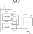
- a power supply system 1 includes power supply apparatuses 10a, 10b.
- the power supply apparatuses 10a, 10b are referred to as a power supply apparatus 10 when no distinction therebetween is necessary.
- the power supply apparatus 10a includes an output terminal 11a and a ground terminal 12a.
- the power supply apparatus 10b includes an output terminal 11b and a ground terminal 12b.
- the output terminals 11a, 11b are referred to as an output terminal 11 when no distinction therebetween is necessary.
- the ground terminals 12a, 12b are referred to as a ground terminal 12 when no distinction therebetween is necessary.
- the power supply apparatuses 10a, 10b are connected to a load 70 in parallel.
- One terminal of the load 70 is connected to the output terminals 11a, 11b.
- the other terminal of the load 70 is connected to a ground point 80 and to the ground terminals 12a, 12b.
- the current outputted by the power supply apparatus 10a from the output terminal 11a is represented as I1.
- the current outputted by the power supply apparatus 10b from the output terminal 11b is represented as I2.
- the power supply system 1 supplies the load 70 with the current yielded by combining the current outputted by the power supply apparatus 10a from the output terminal 11a and the current outputted by the power supply apparatus 10b from the output terminal 11b. In other words, the power supply system 1 provides the current represented as I1 + I2 to the load 70.
- the current supplied to the load 70 may flow to the ground point 80 or may return to the power supply apparatuses 10a, 10b through the ground terminals 12a, 12b.
- the present embodiment is described below assuming that two power supply apparatuses 10 are connected to the load 70 in parallel. Three or more power supply apparatuses 10 may instead be connected to the load 70 in parallel.
- each power supply apparatus 10 When the two power supply apparatuses 10 are connected in parallel to the load 70, and one power supply apparatus 10 fails, then the other power supply apparatus 10 supplies power to the load 70.
- the power supply system 1 overall thereby continues to supply power to the load 70.
- the current outputted by each power supply apparatus 10 when both power supply apparatuses 10 are operating normally may be controlled to be 50% of the current required by the load 70.
- the current required by the load 70 is thereby supplied from the two power supply apparatuses 10 in a balanced manner.
- the current outputted by each power supply apparatus 10 is referred to as the load current I L .
- the maximum current required by the load 70 is referred to as the maximum load current.
- each power supply apparatus 10 is controlled so that the sum of the load currents I L becomes the maximum load current. In the present embodiment, the load 70 is assumed to require the maximum load current.
- the power supply apparatus 10 includes a converter 20, a current detector 30, a FET 40, and a voltage monitor 50.
- the converter 20 includes a converter output terminal 21, a converter ground terminal 22, and a feedback terminal 23.
- the converter 20 outputs the load current I L from the converter output terminal 21 towards the output terminal 11.
- the current detector 30 and the FET 40 are connected in series between the converter output terminal 21 and the output terminal 11.
- the load current I L outputted from the converter output terminal 21 flows through the current detector 30 and the FET 40 and is outputted from the output terminal 11 to the load 70.
- the power supply apparatus 10 outputs the load current I L from the output terminal 11 that is connected to one terminal of the load 70.
- the power supply apparatus 10 outputs an output voltage V out between the output terminal 11 and the ground terminal 12.
- the output voltage V out corresponds to the voltage yielded by subtracting the voltage drop due to the load current I L flowing through the current detector 30 and the FET 40 from the voltage outputted by the converter 20 between the converter output terminal 21 and the converter ground terminal 22.
- the voltage outputted by the converter 20 between the converter output terminal 21 and the converter ground terminal 22 is also referred to as the converter voltage V CONV .
- the converter 20 controls the converter voltage V CONV based on a signal inputted to the feedback terminal 23.
- the current detector 30 detects the load current I L flowing from the converter output terminal 21 to the output terminal 11. Based on the detected load current I L , the current detector 30 generates a current signal I D to input to the feedback terminal 23. As described below, the converter 20 feeds the inputted current signal I D back to the control of the converter voltage V CONV .
- the FET 40 is driven by receiving power from the power supply, represented as VCC. Based on the signal outputted by the current detector 30, the FET 40 controls the current that flows between the converter output terminal 21 and the output terminal 11.
- the FET 40 is assumed to be an n-channel metal oxide silicon FET (MOSFET), but this example is not limiting.
- the FET 40 includes a body diode. The FET 40 is connected so that the forward direction of the body diode matches the direction in which the load current I L flows from the converter 20 towards the load 70.
- the FET 40 is also referred to as a redundancy FET.
- the voltage monitor 50 detects the voltage across both ends of the FET 40. Based on the detection result, the voltage monitor 50 controls the opening and closing of a switching element Q14. When closed, the switching element Q14 creates a short circuit between the source and gate of the FET 40.
- the converter 20 includes a controller 24, an error amplifier 25, and a voltage converter 26.
- the converter 20 converts the power supplied from an external power supply V IN to direct current (DC) power identified by the load current I L and the converter voltage V CONV .
- the voltage converter 26 includes a switching element Q1, a diode D1, an inductor L1, and a capacitor C1.
- the switching element Q1 is assumed to be an n-channel MOSFET, but this example is not limiting.
- the drain of the switching element Q1 is connected to the external power supply V IN .
- the external power supply V IN is represented as a DC power supply but may instead be an alternating current (AC) power supply.
- the source of the switching element Q1 is connected to the cathode of the diode D1 and one terminal of the inductor L1.
- the gate of the switching element Q1 is connected to the controller 24.
- the other terminal of the inductor L1 is connected to one terminal of the capacitor C1.
- the anode of the diode D1 and the other terminal of the capacitor C1 are connected to the ground point 80.
- the switching element Q1 converts the voltage of the external power supply V IN to an AC signal by switching between being open and closed based on a control signal from the controller 24.
- the controller 24 may control the AC signal by a pulse width modulation (PWM) method or by another modulation method.
- PWM pulse width modulation
- the switching element Q1 is assumed to generate a PWM signal controlled by a PWM method.
- the PWM signal is rectified by the diode D1 and is smoothed by the inductor L1 and the capacitor C1 to be converted to DC voltage having a predetermined voltage level.
- the voltage converter 26 forms a step-down switching power supply that steps down the voltage of the external power supply V IN . As the duty ratio of the PWM signal is larger, the voltage level of the DC voltage outputted by the voltage converter 26 increases.
- the voltage converter 26 may be a boost switching power supply.
- the node of the voltage converter 26 between the inductor L1 and the capacitor C1 is connected to the converter output terminal 21.
- the DC voltage outputted by the voltage converter 26 is outputted from the converter output terminal 21 as the converter voltage V CONV .
- the error amplifier 25 includes an operational amplifier U1, resistors R121, R122, and a reference power supply V ref .
- the resistors R121, R122 are connected in series between the converter output terminal 21 and the converter ground terminal 22.
- the node between the resistor R121 and the resistor R122 is connected to an inverting input terminal of the operational amplifier U1.
- the voltage of the node between the resistor R121 and the resistor R122 corresponds to a voltage yielded by dividing the converter voltage V CONV .
- the voltage yielded by dividing the converter voltage V CONV is inputted to the inverting input terminal of the operational amplifier U1.
- the reference power supply V ref is connected to a non-inverting input terminal of the operational amplifier U1.
- the voltage of the reference power supply V ref is inputted to the non-inverting input terminal of the operational amplifier U1.
- the output terminal of the operational amplifier U1 is connected to the inverting input terminal of the operational amplifier U1 via a feedback circuit.
- the feedback circuit may include a resistor and a capacitor.
- the output terminal of the operational amplifier U1 is connected to the controller 24.
- the operational amplifier U1 operates so that the voltage inputted to the inverting input terminal matches the voltage inputted to the non-inverting input terminal.
- the operational amplifier U1 outputs a signal, to the controller 24, for matching the voltage of the node between the resistor R121 and the resistor R122 to the voltage of the reference power supply V ref .
- the controller 24 Based on the output of the operational amplifier U1, the controller 24 outputs a control signal for controlling the opening and closing of the switching element Q1 to the gate of the switching element Q1.
- the controller 24 can control the converter voltage V CONV by using the PWM method to control the AC signal outputted by the switching element Q1.
- the controller 24 may include a processor such as a central processing unit (CPU).
- the controller 24 may control the converter voltage V CONV by executing a predetermined program.
- the converter 20 controls the converter voltage V CONV based on the voltage of the reference power supply V ref .
- the current signal I D flows to the ground point 80 via the resistor R122.
- the current signal I D flows to the resistor R122 superimposed on current that is based on the converter voltage V CONV .
- the current signal I D is also referred to as a superimposed current signal.
- the voltage of the node between the resistor R121 and the resistor R122 rises as a result of the superimposed current signal flowing to the resistor R122.
- the converter voltage V CONV reduces as the current signal I D grows larger.
- the relationship between the load current I L and the converter voltage V CONV can be appropriately set by the current detector 30 determining the current signal I D based on the load current I L , as described below.
- the current detector 30 includes a resistor Rs connected in series between the converter output terminal 21 and the FET 40.
- the resistor Rs detects the load current I L .
- the resistor Rs is also referred to as a current detection unit.
- the sign of the load current I L is assumed to be positive when current flows from the converter output terminal 21 towards the FET 40.
- the current detector 30 includes a droop characteristic controller 32.
- the droop characteristic controller 32 generates the current signal I D based on the voltage across both ends of the resistor Rs.
- the voltage across both ends of the resistor Rs corresponds to the magnitude of the voltage drop occurring due to the current flowing through the resistor Rs and is expressed as the product of Rs and I L .
- the potential at the converter 20 side of the resistor Rs is expressed as V CONV .
- the potential at the FET 40 side of the resistor Rs is expressed as V CONV - Rs ⁇ I L .
- the potential at each end of the resistor Rs is expressed as the potential difference from the ground point 80.
- the droop characteristic controller 32 includes operational amplifiers U13B, U13C, U13D, resistors R135, R136, R137, R138, a Zener diode REFN, and a switching element Q139.
- the terminal of the resistor Rs on the FET 40 side is connected to a non-inverting input terminal of the operational amplifier U13B.
- the terminal of the resistor Rs on the converter 20 side is connected to the inverting input terminal of the operational amplifier U13B via the resistor R136 and is also connected to the inverting input terminal of the operational amplifier U13B via the Zener diode REFN and the resistor R135.
- the resistor R136 and the series connection circuit including the Zener diode REFN and the resistor R135 are connected in parallel between the terminal of the resistor Rs on the converter 20 side and the inverting input terminal of the operational amplifier U13B.
- the output terminal of the operational amplifier U13B is connected to the inverting input terminal of the operational amplifier U13B via the resistor R137.
- the operational amplifier U13B controls output so that the voltage inputted to the inverting input terminal matches the voltage inputted to the non-inverting input terminal.
- the operational amplifier U13B controls the output voltage V B of its output terminal to be the value represented by Expression (1) below.
- V B V CONV + R 137 / R 135 ⁇ REFN ⁇ Rs ⁇ I L ⁇ 1 + R 137 / R 135 / / R 136
- R135//R136 represents the parallel resistance between the resistor R135 and the resistor R136.
- the operational amplifier U13C is connected to the Zener diode REFN and the operational amplifiers U13B, U13D and clamps the lower limit of the voltage inputted to the non-inverting input terminal of the operational amplifier U13D to a predetermined value.
- the non-inverting input terminal of the operational amplifier U13C is connected to the Zener diode REFN.
- the voltage inputted to the non-inverting input terminal of the operational amplifier U13C is represented by V CONV - REFN.
- the inverting input terminal of the operational amplifier U13C is connected to the non-inverting input terminal of the operational amplifier U13D and is also connected to the output terminal of the operational amplifier U13C via a diode.
- the output terminal of the operational amplifier U13C is connected, via a diode, to the inverting input terminal of the operational amplifier U13C and the non-inverting input terminal of the operational amplifier U13D.
- the output terminal of the operational amplifier U13C is further connected to the output terminal of the operational amplifier U13B via a resistor.
- the diode connected to the output terminal of the operational amplifier U13C is connected so that current from the output terminal of the operational amplifier U13C flows in the forward direction. By being connected in this way, the operational amplifier U13C clamps the lower limit of the voltage inputted to the non-inverting input terminal of the operational amplifier U13D at V CONV - REFN.
- the operational amplifier U13D is connected to the operational amplifiers U13B, U13C, the resistor R138, and the switching element Q139.
- the switching element Q139 is assumed to be a p-channel MOSFET, but this example is not limiting.
- the operational amplifier U13D and the switching element Q139 generate a current signal I D based on the load current I L .
- the non-inverting input terminal of the operational amplifier U13D is connected to the output terminals of the operational amplifiers U13B and U13C.
- the voltage inputted to the non-inverting input terminal of the operational amplifier U13D is designated V D .
- the inverting input terminal of the operational amplifier U13D is connected to the converter 20 side of the resistor Rs via the resistor R138 and also to the source of the switching element Q139.
- the output terminal of the operational amplifier U13D is connected to the gate of the switching element Q139.
- the drain of the switching element Q139 is connected to the feedback terminal 23 of the converter 20.
- the operational amplifier U13D controls the current signal I D that flows from the drain of the switching element Q139 to the feedback terminal 23.
- the current signal I D is controlled in three different ways, indicated by cases 1 to 3 below, based on the magnitude of the load current I L .
- the value of the load current I L that differentiates between case 1 and case 2 is also referred to as a first threshold current.
- the value of the load current I L that differentiates between case 2 and case 3 is also referred to as a second threshold current.
- the current signal I D is not outputted until the load current I L reaches the first threshold current.
- the current signal I D increases as the load current I L increases while the load current I L is larger than the first threshold current but does not reach the second threshold current.
- Expression (4) the current signal I D becomes constant once the load current I L exceeds the second threshold current.
- the converter 20 controls the converter voltage V CONV based on the current signal I D inputted to the feedback terminal 23.
- the converter voltage V CONV decreases as the current signal I D increases.
- the load current I L is in the range specified by case 1
- the converter voltage V CONV does not decrease.
- the load current I L is in the range specified by case 2
- the amount of decrease in the converter voltage V CONV is larger as the load current I L increases.
- the load current I L is in the range specified by case 3
- the amount of decrease in the converter voltage V CONV becomes constant.
- the relationship between the load current I L and the current signal I D identified by Expressions (2) to (4) is determined, for example as in the graph in FIG. 6 .
- the horizontal axis represents the load current I L
- the vertical axis represents the output voltage V out in the graph in FIG. 6 .
- the plot labeled Typ characteristics represents typical current-voltage characteristics based on a configuration according to the present embodiment.
- the plots labeled Max variation characteristics and Min variation characteristics represent the assumed upper limit and lower limit on current-voltage characteristics within the possible range of variation exhibited by parameters such as FETs or operational amplifiers in the configuration according to the present embodiment.
- the plot labeled Typ characteristics is assumed below to represent the current-voltage characteristics according to the present embodiment.
- a rated current is set as part of the specifications of the power supply apparatus 10.
- the rated current represents the upper limit of the current at which the power supply apparatus 10 can operate stably. In other words, operations of the power supply apparatus 10 are stable when the power supply apparatus 10 outputs current at or below the rated current. Conversely, operations of the power supply apparatus 10 may become unstable if the power supply apparatus 10 outputs current exceeding the rated current.
- the rated current is indicated by I rate on the horizontal axis of the graph in FIG. 6 .
- the upper limit of the load current I L of the power supply apparatus 10 is the maximum load current.
- the rated current is set to a larger value than the maximum load current.
- the rated current may be the same value as the maximum load current.
- the maximum load current is indicated by 100% (I Lmax ) on the horizontal axis of the graph in FIG. 6 .
- the ratio of the load current I L to the maximum load current is also referred to as the load factor.
- the horizontal axis of the graph in FIG. 6 represents the value of the load current I L along with the load factor.
- Each power supply apparatus 10 is controlled so that the sum of the load currents I L becomes the maximum load current. For example, when two power supply apparatuses 10 are connected to the load 70 in parallel, and the load factor of one power supply apparatus 10 is 60%, then the load factor of the other power supply apparatus 10 is 40%.
- an overload protection (OLP) point is set for protecting the power supply apparatus 10 from overload.
- the power supply apparatus 10 executes an overload protection operation and suspends power supply to the load 70.
- the plot representing the current-voltage characteristics according to the present embodiment includes a region in which the output voltage V out hardly changes despite an increase in the load current I L and a region in which the output voltage V out decreases as the load current I L increases.
- the region in which the output voltage V out decreases as the load current I L increases is also referred to as a droop region.
- the range of the droop region is represented by the shaded area.
- the droop characteristic controller 32 can be considered to cause the output voltage V out to droop in accordance with an increase in the load current I L in the droop region.
- the droop region and other regions may be distinguished between by the slope of the plot.
- the slope of the plot represents the rate of change in the output voltage V out relative to change in the load current I L .
- the rate at which the output voltage V out reduces relative to an increase in the load current I L is also referred to as the droop rate.
- the absolute value of the slope of the plot in the droop region is greater than the slope of the plot in other regions. In other words, the output voltage V out decreases more in the droop region.
- the slope of the plot changes suddenly at two locations.
- the point at which the slope first changes suddenly after the load current I L starts to increase from zero is represented as P1.
- the load current I L at P1 corresponds to the first threshold current.
- the point at which the load current I L becomes a larger value than the first threshold current and the slope suddenly changes for the second time is represented as P2.
- the load current I L at P2 corresponds to the second threshold current.
- the horizontal axis of the graph in FIG. 6 is divided into a plurality of sections with the first threshold current and the second threshold current as boundaries.
- the section in which the current is larger than the first threshold current and smaller than the second threshold current is the section that identifies the droop region. This section is referred to as the first current section.
- the section in which the current is smaller than the first threshold current is referred to as the second current section.
- the section in which the current is larger than the second threshold current is referred to as the third current section.
- the second current section includes a current that is smaller than the current included in the first current section.
- the third current section includes a current that is larger than the current included in the first current section.
- the first threshold current is set to a smaller value than 50% of the maximum load current, but this example is not limiting.
- the first threshold current may be set to any value smaller than the second threshold current.
- the second threshold current is set to a larger value than 50% of the maximum load current, but this example is not limiting.
- the second threshold current may be set to any value larger than the first threshold current.
- the graph in FIG. 7 represents the relationship between the load current I L and the output voltage V out in the above-described configuration of the second comparative example.
- the horizontal axis represents the load current I L
- the vertical axis represents the output voltage V out in the graph in FIG. 7 .
- the plot labeled Typ characteristics represents typical current-voltage characteristics in the second comparative example.
- the plots labeled Max variation characteristics and Min variation characteristics represent the assumed upper limit and lower limit on current-voltage characteristics within the possible range of variation exhibited by parameters such as FETs or operational amplifiers in the configuration according to the second comparative example.
- the output voltage V out reduces in the plot labeled Typ characteristics once the load current I L begins to increase from zero. The slope of the plot changes suddenly at one point.
- the load current I L outputted by each power supply apparatus 10 tends to be stable within the droop region when two power supply apparatuses 10 are connected to the load 70 in parallel.
- the droop region includes the case of the load factor being 0%.
- the load factor of one power supply apparatus 10 in this case may stabilize at or near 0%, or may stabilize at 50%. If the load factor of one power supply apparatus 10 stabilizes at 10%, the load factor of the other power supply apparatus stabilizes at 90%. In other words, the load factor of the power supply apparatus 10 could become unstable in the configuration of the second comparative example.
- the droop region in the configuration according to the present embodiment is limited to a load factor that is larger than the first threshold current and smaller than the second threshold current.
- the load factor of the power supply apparatus 10 is more stable than in the second comparative example. Consequently, the power supply apparatus 10 according to the present embodiment can improve the balance of the load currents I L .
- each of the two power supply apparatuses 10 is controlled to reduce the difference between the load currents I L . In other words, it becomes easier to balance the load currents I L of the two power supply apparatuses 10.
- I Bmax and I Bmin are indicated on the horizontal axis of the graphs in FIGS. 6 and 7 .
- the current outputted by each power supply apparatus 10 falls between I Bmax and I Bmin when two power supply apparatuses 10 connected in parallel to the load 70 output current that is 100% of the maximum load current to the load 70.
- the difference between I Bmax and I Bmin represents the variation in the load factor of the power supply apparatus 10.
- the range from I Bmin to I Bmax is referred to as the variation range of current balance at 100% load.
- the variation in the load factor of the power supply apparatus 10 is smaller.
- a small variation in the load factor makes it easier to improve the balance of the load currents I L .
- the variation in the load factor within the current-voltage characteristics according to the present embodiment is smaller than the variation in the load factor within the current-voltage characteristics according to the second comparative example. Consequently, the power supply apparatus 10 according to the present embodiment can more easily improve the balance of the load currents I L than the second comparative example.
- the difference between I Bmax and I Bmin is smaller as the slope of the plot is sharper.
- the variation in the load factor can be made smaller as the droop rate is greater.
- the variation in the amount of heat generated inside each power supply apparatus 10 can be reduced by the load factors of the two power supply apparatuses 10 being balanced.
- the power supply apparatus 10 includes the FET 40 instead of the redundancy diode 912 of the first comparative example.
- the loss due to the ON resistance of a FET is smaller than the loss due to the voltage drop of a diode. For example, if the ON resistance of the FET 40 is 5 m ⁇ , then the loss becomes 0.5 W when the load current I L is 10 A. On the other hand, if the voltage drop at the redundancy diode 912 of the first comparative example is 0.4 V, then the loss becomes 4 W when the current outputted by the power supply apparatus 91 is 10 A.
- the power supply apparatus 10 according to the present embodiment can, in other words, reduce loss by including the FET 40. The reduction in loss makes heat dissipation components, such as a heatsink, unnecessary and also leads to an improvement in reliability. Consequently, a reduction in size and an improvement in reliability of the power supply apparatus 10 can be achieved.
- the ON resistance of the FET 40 in the present embodiment is low, which lowers the voltage drop at the FET 40. In other words, even when the output voltage V out is controlled based on the result of detecting the voltage of the stage prior to the FET 40, the regulation characteristics of the voltage of the stage subsequent to the FET 40 are not easily affected by the voltage drop. Even if the ON resistance of the FET 40 changes based on temperature characteristics, or if the ON resistance exhibits variation due to individual differences between FETs 40, the change in the output voltage V out caused by these factors is smaller than the change in the output voltage V out caused by the temperature characteristics of the redundancy diode 912. A small change in the output voltage V out makes it easier for the regulation of the output voltage V out to satisfy standards. Consequently, adjustment of the output voltage V out at the time of assembly of the power supply apparatus 10 can be omitted. Manufacturing costs can thereby be reduced.
- the ON resistance of the FET 40 typically has positive temperature characteristics.
- the redundancy diode 912 of the first comparative example has negative temperature characteristics, causing positive feedback with respect to an increase in the current outputted by the power supply apparatus 91. This tends to destabilize or worsen the load balance.
- the ON resistance of the FET 40 has positive temperature characteristics, causing negative feedback with respect to an increase in the load current I L . Consequently, the load balance tends to be stable.
- the current detector 30 includes a separation unit 34, as illustrated in FIG. 5 .
- the separation unit 34 includes an operational amplifier U13A, resistors R131, R132, and a Zener diode REFP.
- the load current I L flows from the converter 20 towards the FET 40.
- the potential of the resistor Rs on the converter 20 side is higher than the potential of the resistor Rs on the FET 40 side.
- a non-inverting input terminal of the operational amplifier U13A is connected to the cathode side of the Zener diode REFP via the resistor R131 and is connected to the converter 20 side of the resistor Rs via the resistor R132.
- the voltage inputted to the non-inverting input terminal of the operational amplifier U13A is the result of adding, to V CONV , the voltage of the Zener diode REFP divided at the resistors R131, R132.
- the inverting input terminal of the operational amplifier U13A is connected to the FET 40 side of the resistor Rs.
- the voltage inputted to the inverting input terminal of the operational amplifier U13A is V CONV - Rs ⁇ I L .
- the output terminal of the operational amplifier U13A is connected to the inverting input terminal via a feedback circuit that includes a resistor and a capacitor and is connected to the gate of the FET 40.
- the operational amplifier U13A limits the current flowing from the FET 40 towards the converter 20 to be a predetermined value or less.
- the current flowing from the FET 40 to the converter 20 is also referred to as reverse current.
- the upper limit of the reverse current controlled by the operational amplifier U13A is referred to as the reverse current limit I bk .
- the sign of I bk is negative when current flows from the FET 40 towards the converter 20.
- I bk is represented by Expression (5) below based on how the non-inverting input terminal and the inverting input terminal of the operational amplifier U13A form a virtual short.
- I bk ⁇ REFP ⁇ R 132 / R 131 + R 132 / Rs
- the operational amplifier U13A can limit the reverse current to be I bk or less by controlling the voltage between the gate and source of the FET 40. If the cause of reverse current flowing to the resistor Rs is temporary, it is required that the FET 40 return to the on state when the cause is resolved. The FET 40 turns on automatically in the configuration whereby the operational amplifier U13A limits the reverse current.
- the voltage monitor 50 includes an operational amplifier U14 and resistors R141, R142, R143.
- the voltage monitor 50 is connected to the switching element Q14.
- the switching element Q14 is assumed to be an n-channel MOSFET, but this example is not limiting.
- the source of the switching element Q14 is connected to the source of the FET 40.
- the drain of the switching element Q14 is connected to the gate of the FET 40.
- the gate of the switching element Q14 is connected to the output terminal of the operational amplifier U14.
- the switching element Q14 turns on.
- the switching element Q14 is on, the source and gate of the FET 40 short circuit.
- the voltage monitor 50 limits the reverse current by controlling the state of the switching element Q14.
- the non-inverting input terminal of the operational amplifier U14 is connected to the drain of the FET 40 via the resistor R143.
- the voltage inputted to the non-inverting input terminal of the operational amplifier U14 is the voltage of the drain of the FET 40.
- the inverting input terminal of the operational amplifier U14 is connected to the source of the FET 40 via the resistor R142 and is connected to the cathode of the Zener diode REFP (see FIG. 5 ) via the resistor R141.
- the voltage inputted to the inverting input terminal of the operational amplifier U14 is the result of adding, to the voltage of the source of the FET 40, the voltage of the Zener diode REFP divided at the resistors R141, R142.
- the voltage of the Zener diode REFP divided at the resistors R141, R142 is also referred to as a monitoring offset voltage.
- the operational amplifier U14 can detect the reverse current based on the voltage between the source and the gate of the FET 40.
- the load current I L flows from the source to the drain of the FET 40.
- the voltage of the source of the FET 40 is higher than the voltage of the drain.
- the voltage inputted to the inverting input terminal of the operational amplifier U14 becomes higher than the voltage inputted to the non-inverting input terminal.
- the voltage that the output terminal of the operational amplifier U14 outputs to the gate of the switching element Q14 becomes 0. Consequently, the switching element Q14 turns off.
- the voltage of the source of the FET 40 becomes lower than the voltage of the drain.
- the difference between the voltage of the drain and the voltage of the source of the FET 40 becomes larger than the voltage of the Zener diode REFP divided by the resistors R141, R142
- the output terminal of the operational amplifier U14 outputs positive voltage to the gate of the switching element Q14.
- the source and gate of the FET 40 short circuit.
- the FET 40 turns off due to the short circuiting of the source and gate of the FET 40. Consequently, the reverse current flowing to the FET 40 is cut off.
- the FET 40 When the internal voltage applied to the source side of the FET 40 reduces due to internal failure of the converter 20 or the like upon the reverse current being cut off at the FET 40, the FET 40 is maintained in the off state by the output voltage of the other power supply apparatus 10 at the drain side of the FET 40 being applied.
- the operational amplifier U14 compares the voltage of the drain of the FET 40 with the sum of the voltage of the source of the FET 40 and the monitoring offset voltage and outputs a signal based on the result of comparison to the gate of the switching element Q14.
- the switching element Q14 controls the resistance between the source and gate of the FET 40 based on the signal inputted to the gate.
- the voltage monitor 50 inputs, to the gate of the FET 40, a signal based on the result of comparing the voltage of the drain of the FET 40 with the sum of the voltage of the source of the FET 40 and the monitoring offset voltage. The reverse current is consequently controlled.
- a reverse current threshold I Loff at which the reverse current is cut off is expressed by Expression (7) below.
- I Loff ⁇ REFP ⁇ R 142 / R 141 + R 142 / R on
- the reverse current threshold I Loff is assumed to be a positive value when current flows from the source to the drain of the FET 40.
- R on represents the ON resistance of the FET 40.
- the power supply apparatus 10 in which reverse current is not flowing is not stopped by the overload protection function. Consequently, the power supply system 1 overall can continue to supply power to the load 70. In other words, when power supply apparatuses 10 for which Expression (8) holds are adjoined and connected in parallel to the load 70, then the overall operation of the power supply system 1 is maintained even if reverse current flows into one of the power supply apparatuses 10.
- the length of time that current with a magnitude of I Loff flows is limited by the FET 40 turning off to cut off reverse current when reverse current in the power supply apparatus 10 exceeds I Loff . In this way, output of current exceeding the rated current of the power supply apparatus 10 is permitted for a limited time.
- the configuration combining the voltage monitor 50 and the switching element Q14 may be replaced with a synchronous rectification control IC.
- the function for the voltage monitor 50 and the switching element Q14 to limit the reverse current and the function for the separation unit 34 to limit the reverse current can replace each other. Accordingly, the power supply apparatus 10 can limit the reverse current and improve reliability by including at least one of the configuration combining the voltage monitor 50 and the switching element Q14 and the configuration of the separation unit 34.
- the configuration combining the voltage monitor 50 and the switching element Q14 and the configuration of the separation unit 34 are also referred to as a reverse current limitation unit.
- the reverse current limit I bk and the reverse current threshold I Loff are also referred to as a reverse current reference limit.
- the FET 40 turns off.
- the loss in the FET 40 when a short-circuit failure occurs is therefore reduced or brought nearly to zero.
- the reduction of loss in the FET 40 reduces the probability of chain-reaction failure in the other power supply apparatus 10 connected in parallel to the load 70.
- the operational amplifier U14 sometimes includes a grounding unit to be grounded to the ground point 80.
- the operational amplifier U14 forms a bridge between the path for outputting the load current I L of the power supply apparatus 10 and the ground point 80.
- other circuit components included in the current detector 30 might form a bridge between the path for outputting the load current I L of the power supply apparatus 10 and the ground point 80.
- a component that forms a bridge between the path for outputting the load current I L of the power supply apparatus 10 and the ground point 80 is also referred to as a bridge component.
- a path that forms a bridge between the path for outputting the load current I L of the power supply apparatus 10 and the ground point 80 is also referred to as a bridge path.
- short-circuit current flows in the bridge path.
- the path for outputting the load current I L of the power supply apparatus 10 and the ground point 80 short circuit. Consequently, short-circuit current flows from the path for outputting the load current I L to the ground point 80.
- the resistor R143 limits the short-circuit current passing through the non-inverting input terminal.
- the resistor R142 limits the short-circuit current passing through the inverting input terminal.
- a resistance element may be connected in series in the bridge path not only in the operational amplifier U14 but also in any other bridge component for the resistance element to limit the short-circuit current due to short-circuit failure of the bridge component.
- a resistance element connected in series in the bridge path facilitates continued operations of the power supply apparatus 10. Consequently, the reliability of the power supply apparatus 10 increases.
- the reliability of the power supply system 1 increases when the power supply system 1 is configured by connecting power supply apparatuses 10 according to the present embodiment in parallel to the load 70.
- the power supply apparatus 10 according to the present embodiment can achieve various functions for improving reliability without use of an MCU. Apparatus costs can be reduced by the omission of an MCU.
- a power supply system 1 includes power supply apparatuses 10a, 10b, 10c.
- the power supply apparatuses 10a, 10b are assumed to be the same as the power supply apparatuses 10a, 10b illustrated in FIG. 2 .
- the power supply apparatuses 10a, 10b, 10c are referred to as a power supply apparatus 10 when no distinction therebetween is necessary.
- the power supply apparatus 10c includes an output terminal 11c and a ground terminal 12c.
- the output terminals 11a, 11b, 11c are referred to as an output terminal 11 when no distinction therebetween is necessary.
- the ground terminals 12a, 12b, 12c are referred to as a ground terminal 12 when no distinction therebetween is necessary.
- the power supply apparatuses 10a, 10b, 10c are connected to a load 70 in parallel.
- One terminal of the load 70 is connected to the output terminals 11a, 11b, 11c.
- the other terminal of the load 70 is connected to a ground point 80 and to the ground terminals 12a, 12b, 12c.
- the current outputted by the power supply apparatus 10a from the output terminal 11a is represented as I1.
- the current outputted by the power supply apparatus 10b from the output terminal 11b is represented as I2.
- the current outputted by the power supply apparatus 10c from the output terminal 11c is represented as I3.
- the power supply system 1 supplies the load 70 with the current yielded by combining the current outputted by the power supply apparatus 10a from the output terminal 11a, the current outputted by the power supply apparatus 10b from the output terminal 11b, and the current outputted by the power supply apparatus 10c from the output terminal 11c.
- the power supply system 1 provides the current represented as I1 + I2 + I3 to the load 70.
- the current supplied to the load 70 may flow to the ground point 80 or may return to the power supply apparatuses 10a, 10b, 10c through the ground terminals 12a, 12b, 12c.
- each power supply apparatus 10 When the three power supply apparatuses 10 are connected in parallel to the load 70, and one power supply apparatus 10 fails, then another power supply apparatus 10 supplies power to the load 70.
- the power supply system 1 overall thereby continues to supply power to the load 70.
- the current outputted by each power supply apparatus 10 when all three power supply apparatuses 10 are operating normally may be controlled to be 1/3 of the current required by the load 70.
- the current required by the load 70 is thereby supplied from the three power supply apparatuses 10 in a balanced manner.
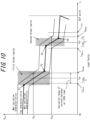
- the relationship between the load current I L and the output voltage V out in the power supply apparatus 10 according to the present embodiment is, for example, determined as in the graph of FIG. 10 .
- the horizontal axis represents the load current I L
- the vertical axis represents the output voltage V out in the graph in FIG. 10 .
- the plot labeled Typ characteristics represents typical current-voltage characteristics based on a configuration according to the present embodiment.
- the plots labeled Max variation characteristics and Min variation characteristics represent the assumed upper limit and lower limit on current-voltage characteristics within the possible range of variation exhibited by parameters such as FETs or operational amplifiers in the configuration according to the present embodiment.
- the plot labeled Typ characteristics is assumed below to represent the current-voltage characteristics according to the present embodiment.
- the slope of the plot changes suddenly at four locations.
- the point at which the slope first changes suddenly after the load current I L starts to increase from zero is represented as P1.
- the load current I L at P1 corresponds to a first threshold current.
- the point at which the load current I L becomes a larger value than the first threshold current and the slope suddenly changes for the second time is represented as P2.
- the load current I L at P2 corresponds to a second threshold current.
- the point at which the load current I L becomes a larger value than the second threshold current and the slope suddenly changes for the third time is represented as P3.
- the load current I L at P3 corresponds to a third threshold current.
- the point at which the load current I L becomes a larger value than the third threshold current and the slope suddenly changes for the fourth time is represented as P4.
- the load current I L at P4 corresponds to a fourth threshold current.
- the horizontal axis of the graph in FIG. 10 is divided into a plurality of sections with the first threshold current through the fourth threshold current as boundaries.
- the section in which the current is larger than the first threshold current and smaller than the second threshold current is the section that identifies a first droop region. This section is referred to as the first current section.
- the section in which the current is smaller than the first threshold current is referred to as the second current section.
- the section in which the current is larger than the second threshold current and smaller than the third threshold current is referred to as the third current section.
- the section in which the current is larger than the third threshold current and smaller than the fourth threshold current is the section that identifies a second droop region. This section is referred to as the fourth current section.
- the section in which the current is larger than the fourth threshold current is referred to as the fifth current section.
- the second current section includes a current that is smaller than the current included in the first current section.
- the third current section includes a current that is larger than the current included in the first current section and smaller than the current included in the fourth current section.
- the fifth current section includes a current that is larger than the current included in the fourth current section.
- I B1 I Lmax / 3
- I B1max and I B1min are indicated on the horizontal axis of the graph in FIG. 10 .
- I B1max represents the current flowing at the Max variation characteristics
- V B1 represents the voltage outputted by the output terminal of the operational amplifier U13B in the droop characteristic controller 32 when the load currents I L of the three power supply apparatuses 10 are balanced.
- the difference between I B1max and I B1min represents the variation of the load factor that can occur when the load currents I L of the three power supply apparatuses 10 are balanced. In other words, as the difference between I B1max and I B1min is smaller, the variation in the load factor of the three power supply apparatuses 10 is smaller.
- I B2 the current outputted by each of the two power supply apparatuses 10 is referred to as an ideal balanced current I B2 .
- the third threshold current is set to a smaller value than I B2 .
- the fourth threshold current is set to a larger value than I B2 .
- Expression (10) below holds when the maximum reverse current that can flow to one power supply apparatus 10 that has failed is represented by the reverse current limit I bk .
- I B 2 ⁇ I bk + I Lmax / 2
- I B2max and I B2min are indicated on the horizontal axis of the graph in FIG. 10 .
- I B2max represents the current flowing at the Max variation characteristics
- V B2 represents the voltage outputted by the output terminal of the operational amplifier U13B in the droop characteristic controller 32 when one power supply apparatus 10 has failed and the load currents I L of the other two power supply apparatuses 10 are balanced.
- the difference between I B2max and I B2min represents the variation of the load factor that can occur when the load currents I L of the two power supply apparatuses 10 are balanced. In other words, as the difference between I B2max and I B2min is smaller, the variation in the load factor of the two power supply apparatuses 10 is smaller.
- I B2max represents the maximum value of the load current I L that can flow in one of the two power supply apparatuses 10 whose load currents I L are balanced.
- I B2max is larger than I B2 .
- I B2max is required to be equal to or less than the rated current I rate . Therefore, Expression (11) below holds.
- the load currents I L of the operating power supply apparatuses 10 are easier to balance, both when all three power supply apparatuses 10 are operating and when one power supply apparatus 10 has failed. Consequently, the reliability of the power supply system 1 increases.
- the power supply system 1 may include (N + 1) power supply apparatuses 10.
- N is a natural number and is two or more.
- the above-described Expressions (9) to (11) are generalized as Expressions (12) to (14) below.
- I B 1 I Lmax / N + 1
- I B 2 ⁇ I bk + I Lmax / N I rate ⁇ I B 2 max > ⁇ I bk + I Lmax / N
- N + 1 is referred to as a first predetermined number.
- N is referred to as a second predetermined number.
- the second predetermined number is the result of subtracting one from the first predetermined number.
- I B1 is represented as the product of the maximum load current I Lmax and the inverse of the first predetermined number.
- I B2 is represented as the product of (i) the sum of the maximum load current I Lmax and the absolute value of the reverse current limit I bk and (ii) the inverse of the second predetermined number.
- Expression (13) may be replaced by Expression (15) below.
- I B 2 I Lmax / N
- I B2 is represented as the product of the maximum load current I Lmax and the inverse of the second predetermined number.
- a p-channel MOSFET may be used as the FET 40.
- the current detection unit is connected in series to the path over which the load current I L outputted by the converter 20 flows towards the load 70.
- the current detection unit may be connected in series to the path over which the load current I L returns from the load 70 to the converter 20. This allows an operational amplifier that is not rail-to-rail to be used as the operational amplifier that acquires the detection result of the current detection unit in the current detector 30.
Landscapes
- Engineering & Computer Science (AREA)
- Power Engineering (AREA)
- Dc-Dc Converters (AREA)
- Direct Current Feeding And Distribution (AREA)
Description
- The present application claims priority from
Japanese Patent Application No. 2019-53174 filed March 20, 2019 - The present disclosure relates to a power supply system and a power supply apparatus.
- An example of a known power supply apparatus used in a redundant power supply reduces the output voltage as the current outputted to the load increases. For example, see patent literature (PTL) 1.
- Patent
US 6,438,007 B1 describes a control circuit for, and method of, allowing the power supply, having a controller and an output current limit, to be operated in parallel with other power supplies and a power supply incorporating the circuit or the method. In one configuration, the circuit includes: (1) a voltage sense subcircuit, coupled to an output of the power supply, that produces a voltage control signal that is a function of an output voltage of the power supply and a voltage proportional to an output current of the power supply and (2) a current sense subcircuit, coupled to the power supply, that produces a current sense signal that is a function of the output current of the power supply, a combination of the voltage control signal and current control signal employable to modify an output of the controller and thereby regulate said power supply and allow said power supply to continuously operate in a current limit region. - Patent application publication
US 2018/367050 A1 describes a welding power supply with extended voltage characteristic. - Patent application publication
US 2011/107122 A1 describes a power supply and power supply system incorporating a plurality of power supplies. - Patent
US 6,301,133 B1 describes a power supply system with ORing element and control circuit. - Patent application publication
US 2008/062730 A1 describes a method and apparatus for distributing electrical power. - Patent application publication
CN 106533142 A describes a anti-backflow circuit. - PTL 1:
JPH8-289468A - When a redundant power supply is configured by the power supply apparatus disclosed in
PTL 1, the outputs of two power supply apparatuses are directly combined. If one of the power supply apparatuses suffers a short-circuit failure, the voltage supplied to the load might lower. - In light of this point, it would be helpful to provide a power supply system and a power supply apparatus that are highly reliable.
- It is an object of the present invention to provide a power supply apparatus and a power supply system that obviate or mitigate at least one of the disadvantages and shortcomings of the related prior art.
- This object is solved by the present invention as claimed in the appended
claims - A power supply system according to the present invention includes at least two power supply apparatuses that supply current to one load. Each power supply apparatus includes a converter that supplies current to the load, a FET connected in series between the converter and the load, a current detector including a current detection unit configured to detect current flowing between the converter and the load, a droop characteristic controller configured to cause output voltage of the converter to droop at a droop rate determined based on the magnitude of load current flowing from the converter towards the load, and a reverse current limitation unit configured to limit a reverse current flowing from the load towards the converter to be a reverse current limit or less by controlling a voltage between a gate and source of the FET. The FET is configured to control the current outputted from the converter based on a signal outputted by the current detector. The droop rate when the load current is included in a first current section is greater than the droop rate when the load current is included in each of a second current section and a third current section. The second current section includes current that is smaller than current included in the first current section. The third current section includes current that is larger than the current included in the first current section. The load current is easier to balance when the droop rate is thus increased in a predetermined current section. Consequently, the reliability of the power supply system increases.
- In a power supply system according to an embodiment, each power supply apparatus may further include a reverse current limitation unit that limits, based on a reverse current reference limit, a reverse current flowing from the load towards the converter. If one power supply apparatus suffers a short-circuit failure, this configuration reduces the probability of chain-reaction suspension of other operating power supply apparatuses. Consequently, the reliability of the power supply system increases.
- In a power supply system according to an embodiment, the reverse current limitation unit may include a separation unit that inputs, to a gate of the FET, a signal based on the result of comparing the reverse current as detected by the current detection unit with the reverse current reference limit. The reverse current is limited by this configuration to be within a predetermined value. Consequently, the reliability of the power supply system increases.
- In a power supply system according to an embodiment, the reverse current limitation unit may include a voltage monitor that inputs, to the gate of the FET, a signal based on the result of comparing the potential of the drain of the FET with the sum of the potential of the source of the FET and a monitoring offset voltage. The FET is cut off in this configuration when the reverse current exceeds a predetermined value. Consequently, the loss at the FET due to reverse current becomes nearly zero.
- In a power supply system according to an embodiment, the converter may have a rated current. The rated current may be set to a larger value than the sum of the maximum load current and the reverse current reference limit. If reverse current flows in one power supply apparatus, this configuration reduces the probability of chain-reaction suspension of other operating power supply apparatuses. Consequently, the reliability of the power supply system increases.
- In a power supply system according to an embodiment, a resistance element may be connected in series in at least one of paths short-circuiting between a current path from the converter towards the load and a ground point. This configuration limits short-circuit current flowing due to a short-circuit failure inside the power supply apparatus. Consequently, the reliability of the power supply system increases.
- In a power supply system according to an embodiment, the first current section may include a current that is 50% of the maximum load current. This configuration balances the current outputted by each power supply apparatus when two power supply apparatuses are connected to the load. Balanced current reduces the difference in the amount of heat generated inside each power supply apparatus. The difference in lifespan of components in each power supply apparatus thereby reduces, increasing the reliability of the power supply system.
- In a power supply system according to an embodiment, the droop rate when the load current is included in a fourth current section may be greater than the droop rate when the load current is included in each of a fifth current section and the third current section, the fourth current section may include current that is larger than current included in the third current section, the fifth current section may include current that is larger than current included in the fourth current section, the first current section may include current represented by the product of the maximum load current and the inverse of a first predetermined number, and the fourth current section may include current represented by the product of the maximum load current and the inverse of a second predetermined number yielded by subtracting one from the first predetermined number. The currents outputted by operating power supply apparatuses are easier to balance with this configuration, both when all of the first predetermined number of power supply apparatuses connected to the load are operating and when one of the power supply apparatuses has failed. Consequently, the reliability of the power supply system increases.
- A power supply apparatus according to the present invention includes a converter configured to supply current to a load, a FET connected in series between the converter and the load, a current detector including a current detection unit configured to detect current flowing between the converter and the load, a droop characteristic controller configured to cause output voltage of the converter to droop at a droop rate determined based on the magnitude of load current flowing from the converter towards the load, and a reverse current limitation unit configured to limit a reverse current flowing from the load towards the converter to be a reverse current limit or less by controlling a voltage between a gate and source of the FET. The FET is configured to control the current outputted from the converter based on a signal outputted by the current detector. The droop rate when the load current is included in a first current section is greater than the droop rate when the load current is included in each of a second current section and a third current section. The second current section includes current that is smaller than current included in the first current section. The third current section includes current that is larger than the current included in the first current section. The load current is easier to balance when the droop rate is thus increased in a predetermined current section. Consequently, the reliability of the power supply apparatus increases.
- The present disclosure provides a power supply system and a power supply apparatus that are highly reliable.
- The scope of the present invention is defined by the appended claims. Embodiments and/or examples mentioned in the following description that do not fall under the scope of the appended claims are to be construed as comparative examples useful for understanding the present invention.
- In the accompanying drawings:
-
FIG. 1 is a circuit diagram illustrating a power supply system according to a first comparative example; -
FIG. 2 is a block diagram illustrating an example configuration of a power supply system according to an embodiment; -
FIG. 3 is a block diagram illustrating an example configuration of a power supply apparatus according to an embodiment; -
FIG. 4 is a block diagram illustrating an example configuration of a converter; -
FIG. 5 is a block diagram illustrating an example configuration of a current detector; -
FIG. 6 is a graph illustrating an example of a droop characteristic of a power supply apparatus according to an embodiment; -
FIG. 7 is a graph illustrating an example of a droop characteristic of a power supply apparatus according to a second comparative example; -
FIG. 8 is a block diagram illustrating an example configuration of a voltage monitor; -
FIG. 9 is a block diagram illustrating an example configuration of a power supply system according to another embodiment; and -
FIG. 10 is a graph illustrating an example of a droop characteristic of a power supply apparatus according to another embodiment. - Embodiments of the present disclosure are described while being compared to comparative examples.
- As illustrated in
FIG. 1 , apower supply system 90 according to a first comparative example includes apower supply apparatus 91 and apower supply apparatus 92. Thepower supply apparatus 91 includes aconverter 911, aredundancy diode 912, anoutput terminal 913, and aground terminal 914. Thepower supply apparatus 92 includes aconverter 921, aredundancy diode 922, anoutput terminal 923, and aground terminal 924. Matter that is common to thepower supply apparatuses power supply apparatus 91. - The
power supply apparatuses load 70 in parallel. One terminal of theload 70 is connected to theoutput terminals load 70 is connected to aground point 80 and to theground terminals power supply system 90 supplies theload 70 with the current yielded by combining the current outputted by thepower supply apparatus 91 from theoutput terminal 913 and the current outputted by thepower supply apparatus 92 from theoutput terminal 923. The current supplied to theload 70 may flow to theground point 80 or may return to thepower supply apparatuses ground terminals - The
redundancy diodes power supply apparatuses load 70 in parallel via theredundancy diodes redundancy diode 912 prevents current from flowing from theoutput terminal 913 towards theconverter 911. Theredundancy diode 922 prevents current from flowing from theoutput terminal 923 towards theconverter 921. - The
converter 911 controls voltage between theoutput terminal 913 and theground terminal 914. Theconverter 921 controls voltage between theoutput terminal 923 and theground terminal 924. By controlling the voltage of theoutput terminals converters load 70 while balancing the magnitude of the current provided by each of thepower supply apparatuses load 70. - If one of the
power supply apparatuses load 70. For example, when thepower supply apparatus 91 stops, then thepower supply apparatus 92 supplies all of the current required by theload 70. Consequently, even if one of thepower supply apparatuses power supply system 90 overall can maintain the supply of power to theload 70. In other words, thepower supply system 90 is redundant. In this case, each of thepower supply apparatuses load 70. - When the
power supply apparatus 91 is connected to theload 70 via theredundancy diode 912, as in thepower supply system 90, then loss increases at theredundancy diode 912. For example, when the forward voltage drop of theredundancy diode 912 is 0.4 volts (V), then a current of 10 amperes (A) provided to theload 70 generates a loss of up to 4 watts (W) at theredundancy diode 912. Thepower supply apparatus 91 needs to include a heat dissipation member, such as a large heatsink, in this case. The heat dissipation member prevents thepower supply apparatus 91 from being reduced in size. Furthermore, the heat generated at theredundancy diode 912 raises the temperature of electronic components such as an electrolytic capacitor, thereby shortening the lifespan of the electronic components. Consequently, the reliability of thepower supply apparatus 91 decreases. - The
power supply apparatus 91 controls the voltage of the stage prior to theredundancy diode 912. In this case, theredundancy diode 912 is located outside of the feedback loop of the feedback control by thepower supply apparatus 91. Theconverter 911 therefore cannot compensate for the current-voltage characteristics or temperature characteristics of theredundancy diode 912, nor for individual variation in these characteristics. The inability to compensate for the characteristics of theredundancy diode 912 increases the error of the voltage outputted by thepower supply apparatus 91. Consequently, it is difficult for thepower supply apparatus 91 that includes theredundancy diode 912 to control the voltage. In other words, the voltage regulation characteristics of thepower supply apparatus 91 that includes theredundancy diode 912 are poor. - The forward voltage drop of the
redundancy diode 912 typically has negative temperature characteristics. For example, in a Schottky barrier diode with a forward voltage drop of approximately 0.4 V, the difference in the forward voltage drop between the low temperature environment and the high temperature environment might be approximately 0.2 V to 0.3 V. When thepower supply apparatus 91 outputs a voltage of 5 V, for example, and the forward voltage drop changes by 0.2 V to 0.3 V due to the temperature characteristics, then this change causes the output voltage also to change by 4% to 6%. The regulation standard for a typical power supply is roughly ±5%. Accordingly, it is difficult to satisfy the regulation standard in a power supply that includes an element causing the output voltage to change by 4% to 6%. To satisfy the regulation standard, it becomes necessary to use a trimmer resistor or the like for precise adjustment of the voltage setting. This precise adjustment raises manufacturing costs. - The higher the temperature of the
redundancy diode 912, the more the forward voltage drop of theredundancy diode 912 decreases due to the negative temperature characteristics. This decrease in the forward voltage drop of theredundancy diode 912 increases the voltage outputted by thepower supply apparatus 91. In turn, the increase in the voltage outputted by thepower supply apparatus 91 increases the current outputted by thepower supply apparatus 91 to theload 70. The increase in the current outputted by thepower supply apparatus 91 raises the temperature of theredundancy diode 912. In this way, positive feedback may occur in the temperature of theredundancy diode 912. The current outputted by thepower supply apparatus 91 to theload 70 and the current outputted by thepower supply apparatus 92 to theload 70 therefore easily become imbalanced in the configuration that connects to theload 70 via theredundancy diodes - The case of the
power supply apparatuses redundancy diodes power supply apparatuses load 70 increases. When thepower supply apparatuses load 70, the droop characteristic makes it easier to balance the current outputted by each of thepower supply apparatuses redundancy diodes redundancy diodes power supply apparatus 91 suffers a short-circuit failure, for example, the current of thepower supply apparatus 92 flows to the short-circuit point of thepower supply apparatus 91. This leads to effects such as the current supplied from thepower supply apparatus 92 to theload 70 becoming insufficient, or the voltage outputted by thepower supply apparatus 92 decreasing. Thepower supply system 90 overall therefore becomes unable to maintain the supply of power to theload 70. - A configuration in which each of the
power supply apparatuses power supply apparatus 91 needs to include a circuit for detecting the current outputted by another apparatus and a circuit for controlling the outputted current based on the detected current. Such a configuration leads to increased apparatus cost. - A configuration in which the
power supply apparatuses power supply apparatuses load 70 functions as a master, and the other functions as a slave. Based on the detected voltage and current outputted by each apparatus, the MCU of the apparatus functioning as the master outputs control information to the MCU of the apparatus functioning as the slave. This configuration allows the MCU to balance the current outputted by each apparatus and to reduce variation in the voltage. A configuration using an MCU, however, requires that each apparatus detect and communicate the outputted voltage and current. A program to operate the MCU is also required. Use of an MCU therefore leads to an increase in device cost. - As described above, the configurations in the comparative examples have problems such as a difficulty in balancing the current outputted by the
power supply apparatuses power supply system 90 and thepower supply apparatus 91. - The present disclosure therefore describes a highly reliable power supply apparatus and power supply system.
- As illustrated in
FIG. 2 , apower supply system 1 according to an embodiment includespower supply apparatuses power supply apparatuses power supply apparatus 10 when no distinction therebetween is necessary. - The
power supply apparatus 10a includes anoutput terminal 11a and aground terminal 12a. Thepower supply apparatus 10b includes anoutput terminal 11b and aground terminal 12b. Theoutput terminals output terminal 11 when no distinction therebetween is necessary. Theground terminals ground terminal 12 when no distinction therebetween is necessary. - The
power supply apparatuses load 70 in parallel. One terminal of theload 70 is connected to theoutput terminals load 70 is connected to aground point 80 and to theground terminals power supply apparatus 10a from theoutput terminal 11a is represented as I1. The current outputted by thepower supply apparatus 10b from theoutput terminal 11b is represented as I2. Thepower supply system 1 supplies theload 70 with the current yielded by combining the current outputted by thepower supply apparatus 10a from theoutput terminal 11a and the current outputted by thepower supply apparatus 10b from theoutput terminal 11b. In other words, thepower supply system 1 provides the current represented as I1 + I2 to theload 70. The current supplied to theload 70 may flow to theground point 80 or may return to thepower supply apparatuses ground terminals - The present embodiment is described below assuming that two
power supply apparatuses 10 are connected to theload 70 in parallel. Three or morepower supply apparatuses 10 may instead be connected to theload 70 in parallel. - When the two
power supply apparatuses 10 are connected in parallel to theload 70, and onepower supply apparatus 10 fails, then the otherpower supply apparatus 10 supplies power to theload 70. Thepower supply system 1 overall thereby continues to supply power to theload 70. The current outputted by eachpower supply apparatus 10 when bothpower supply apparatuses 10 are operating normally may be controlled to be 50% of the current required by theload 70. The current required by theload 70 is thereby supplied from the twopower supply apparatuses 10 in a balanced manner. The current outputted by eachpower supply apparatus 10 is referred to as the load current IL. The maximum current required by theload 70 is referred to as the maximum load current. When theload 70 requires the maximum load current, eachpower supply apparatus 10 is controlled so that the sum of the load currents IL becomes the maximum load current. In the present embodiment, theload 70 is assumed to require the maximum load current. - As illustrated in
FIG. 3 , thepower supply apparatus 10 includes aconverter 20, acurrent detector 30, aFET 40, and avoltage monitor 50. - The
converter 20 includes aconverter output terminal 21, aconverter ground terminal 22, and afeedback terminal 23. Theconverter 20 outputs the load current IL from theconverter output terminal 21 towards theoutput terminal 11. Thecurrent detector 30 and theFET 40 are connected in series between theconverter output terminal 21 and theoutput terminal 11. The load current IL outputted from theconverter output terminal 21 flows through thecurrent detector 30 and theFET 40 and is outputted from theoutput terminal 11 to theload 70. In other words, thepower supply apparatus 10 outputs the load current IL from theoutput terminal 11 that is connected to one terminal of theload 70. - The
power supply apparatus 10 outputs an output voltage Vout between theoutput terminal 11 and theground terminal 12. The output voltage Vout corresponds to the voltage yielded by subtracting the voltage drop due to the load current IL flowing through thecurrent detector 30 and theFET 40 from the voltage outputted by theconverter 20 between theconverter output terminal 21 and theconverter ground terminal 22. The voltage outputted by theconverter 20 between theconverter output terminal 21 and theconverter ground terminal 22 is also referred to as the converter voltage VCONV. Theconverter 20 controls the converter voltage VCONV based on a signal inputted to thefeedback terminal 23. - The
current detector 30 detects the load current IL flowing from theconverter output terminal 21 to theoutput terminal 11. Based on the detected load current IL, thecurrent detector 30 generates a current signal ID to input to thefeedback terminal 23. As described below, theconverter 20 feeds the inputted current signal ID back to the control of the converter voltage VCONV. - The
FET 40 is driven by receiving power from the power supply, represented as VCC. Based on the signal outputted by thecurrent detector 30, theFET 40 controls the current that flows between theconverter output terminal 21 and theoutput terminal 11. TheFET 40 is assumed to be an n-channel metal oxide silicon FET (MOSFET), but this example is not limiting. TheFET 40 includes a body diode. TheFET 40 is connected so that the forward direction of the body diode matches the direction in which the load current IL flows from theconverter 20 towards theload 70. TheFET 40 is also referred to as a redundancy FET. - The voltage monitor 50 detects the voltage across both ends of the
FET 40. Based on the detection result, the voltage monitor 50 controls the opening and closing of a switching element Q14. When closed, the switching element Q14 creates a short circuit between the source and gate of theFET 40. - As illustrated in
FIG. 4 , theconverter 20 includes acontroller 24, anerror amplifier 25, and avoltage converter 26. Theconverter 20 converts the power supplied from an external power supply VIN to direct current (DC) power identified by the load current IL and the converter voltage VCONV. - The
voltage converter 26 includes a switching element Q1, a diode D1, an inductor L1, and a capacitor C1. The switching element Q1 is assumed to be an n-channel MOSFET, but this example is not limiting. The drain of the switching element Q1 is connected to the external power supply VIN. The external power supply VIN is represented as a DC power supply but may instead be an alternating current (AC) power supply. The source of the switching element Q1 is connected to the cathode of the diode D1 and one terminal of the inductor L1. The gate of the switching element Q1 is connected to thecontroller 24. The other terminal of the inductor L1 is connected to one terminal of the capacitor C1. The anode of the diode D1 and the other terminal of the capacitor C1 are connected to theground point 80. - The switching element Q1 converts the voltage of the external power supply VIN to an AC signal by switching between being open and closed based on a control signal from the
controller 24. Thecontroller 24 may control the AC signal by a pulse width modulation (PWM) method or by another modulation method. The switching element Q1 is assumed to generate a PWM signal controlled by a PWM method. - The PWM signal is rectified by the diode D1 and is smoothed by the inductor L1 and the capacitor C1 to be converted to DC voltage having a predetermined voltage level. In other words, the
voltage converter 26 forms a step-down switching power supply that steps down the voltage of the external power supply VIN. As the duty ratio of the PWM signal is larger, the voltage level of the DC voltage outputted by thevoltage converter 26 increases. Thevoltage converter 26 may be a boost switching power supply. - The node of the
voltage converter 26 between the inductor L1 and the capacitor C1 is connected to theconverter output terminal 21. The DC voltage outputted by thevoltage converter 26 is outputted from theconverter output terminal 21 as the converter voltage VCONV. - The
error amplifier 25 includes an operational amplifier U1, resistors R121, R122, and a reference power supply Vref. - The resistors R121, R122 are connected in series between the
converter output terminal 21 and theconverter ground terminal 22. The node between the resistor R121 and the resistor R122 is connected to an inverting input terminal of the operational amplifier U1. The voltage of the node between the resistor R121 and the resistor R122 corresponds to a voltage yielded by dividing the converter voltage VCONV. In other words, the voltage yielded by dividing the converter voltage VCONV is inputted to the inverting input terminal of the operational amplifier U1. The reference power supply Vref is connected to a non-inverting input terminal of the operational amplifier U1. The voltage of the reference power supply Vref is inputted to the non-inverting input terminal of the operational amplifier U1. The output terminal of the operational amplifier U1 is connected to the inverting input terminal of the operational amplifier U1 via a feedback circuit. The feedback circuit may include a resistor and a capacitor. - The output terminal of the operational amplifier U1 is connected to the
controller 24. The operational amplifier U1 operates so that the voltage inputted to the inverting input terminal matches the voltage inputted to the non-inverting input terminal. The operational amplifier U1 outputs a signal, to thecontroller 24, for matching the voltage of the node between the resistor R121 and the resistor R122 to the voltage of the reference power supply Vref. - Based on the output of the operational amplifier U1, the
controller 24 outputs a control signal for controlling the opening and closing of the switching element Q1 to the gate of the switching element Q1. Thecontroller 24 can control the converter voltage VCONV by using the PWM method to control the AC signal outputted by the switching element Q1. Thecontroller 24 may include a processor such as a central processing unit (CPU). Thecontroller 24 may control the converter voltage VCONV by executing a predetermined program. - When the current signal ID is not inputted to the
feedback terminal 23, theconverter 20 controls the converter voltage VCONV based on the voltage of the reference power supply Vref. When the current signal ID is inputted to thefeedback terminal 23, the current signal ID flows to theground point 80 via the resistor R122. In other words, the current signal ID flows to the resistor R122 superimposed on current that is based on the converter voltage VCONV. The current signal ID is also referred to as a superimposed current signal. The voltage of the node between the resistor R121 and the resistor R122 rises as a result of the superimposed current signal flowing to the resistor R122. As a result of the operations of the operational amplifier U1 and thecontroller 24, the converter voltage VCONV reduces as the current signal ID grows larger. The relationship between the load current IL and the converter voltage VCONV can be appropriately set by thecurrent detector 30 determining the current signal ID based on the load current IL, as described below. - As illustrated in
FIG. 5 , thecurrent detector 30 includes a resistor Rs connected in series between theconverter output terminal 21 and theFET 40. The resistor Rs detects the load current IL. The resistor Rs is also referred to as a current detection unit. The sign of the load current IL is assumed to be positive when current flows from theconverter output terminal 21 towards theFET 40. - The
current detector 30 includes a droopcharacteristic controller 32. The droopcharacteristic controller 32 generates the current signal ID based on the voltage across both ends of the resistor Rs. The voltage across both ends of the resistor Rs corresponds to the magnitude of the voltage drop occurring due to the current flowing through the resistor Rs and is expressed as the product of Rs and IL. The potential at theconverter 20 side of the resistor Rs is expressed as VCONV. The potential at theFET 40 side of the resistor Rs is expressed as VCONV - Rs · IL. The potential at each end of the resistor Rs is expressed as the potential difference from theground point 80. - The droop
characteristic controller 32 includes operational amplifiers U13B, U13C, U13D, resistors R135, R136, R137, R138, a Zener diode REFN, and a switching element Q139. - The terminal of the resistor Rs on the
FET 40 side is connected to a non-inverting input terminal of the operational amplifier U13B. The terminal of the resistor Rs on theconverter 20 side is connected to the inverting input terminal of the operational amplifier U13B via the resistor R136 and is also connected to the inverting input terminal of the operational amplifier U13B via the Zener diode REFN and the resistor R135. In other words, the resistor R136 and the series connection circuit including the Zener diode REFN and the resistor R135 are connected in parallel between the terminal of the resistor Rs on theconverter 20 side and the inverting input terminal of the operational amplifier U13B. The output terminal of the operational amplifier U13B is connected to the inverting input terminal of the operational amplifier U13B via the resistor R137. - The operational amplifier U13B controls output so that the voltage inputted to the inverting input terminal matches the voltage inputted to the non-inverting input terminal. In the example in
FIG. 5 , the operational amplifier U13B controls the output voltage VB of its output terminal to be the value represented by Expression (1) below.
- The operational amplifier U13C is connected to the Zener diode REFN and the operational amplifiers U13B, U13D and clamps the lower limit of the voltage inputted to the non-inverting input terminal of the operational amplifier U13D to a predetermined value. The non-inverting input terminal of the operational amplifier U13C is connected to the Zener diode REFN. The voltage inputted to the non-inverting input terminal of the operational amplifier U13C is represented by VCONV - REFN. The inverting input terminal of the operational amplifier U13C is connected to the non-inverting input terminal of the operational amplifier U13D and is also connected to the output terminal of the operational amplifier U13C via a diode. In other words, the output terminal of the operational amplifier U13C is connected, via a diode, to the inverting input terminal of the operational amplifier U13C and the non-inverting input terminal of the operational amplifier U13D. The output terminal of the operational amplifier U13C is further connected to the output terminal of the operational amplifier U13B via a resistor. The diode connected to the output terminal of the operational amplifier U13C is connected so that current from the output terminal of the operational amplifier U13C flows in the forward direction. By being connected in this way, the operational amplifier U13C clamps the lower limit of the voltage inputted to the non-inverting input terminal of the operational amplifier U13D at VCONV - REFN.
- The operational amplifier U13D is connected to the operational amplifiers U13B, U13C, the resistor R138, and the switching element Q139. The switching element Q139 is assumed to be a p-channel MOSFET, but this example is not limiting. The operational amplifier U13D and the switching element Q139 generate a current signal ID based on the load current IL. The non-inverting input terminal of the operational amplifier U13D is connected to the output terminals of the operational amplifiers U13B and U13C. The voltage inputted to the non-inverting input terminal of the operational amplifier U13D is designated VD. The inverting input terminal of the operational amplifier U13D is connected to the
converter 20 side of the resistor Rs via the resistor R138 and also to the source of the switching element Q139. The output terminal of the operational amplifier U13D is connected to the gate of the switching element Q139. The drain of the switching element Q139 is connected to thefeedback terminal 23 of theconverter 20. The operational amplifier U13D controls the current signal ID that flows from the drain of the switching element Q139 to thefeedback terminal 23. The current signal ID is controlled in three different ways, indicated bycases 1 to 3 below, based on the magnitude of the load current IL. -

- This is the case when the following expression holds.


- This is the case when the following expressions both hold.


- This is the case when the following expression holds.

- The value of the load current IL that differentiates between
case 1 andcase 2 is also referred to as a first threshold current. The value of the load current IL that differentiates betweencase 2 andcase 3 is also referred to as a second threshold current. By Expression (2), the current signal ID is not outputted until the load current IL reaches the first threshold current. By Expression (3), the current signal ID increases as the load current IL increases while the load current IL is larger than the first threshold current but does not reach the second threshold current. By Expression (4), the current signal ID becomes constant once the load current IL exceeds the second threshold current. - The
converter 20 controls the converter voltage VCONV based on the current signal ID inputted to thefeedback terminal 23. The converter voltage VCONV decreases as the current signal ID increases. When the load current IL is in the range specified bycase 1, the converter voltage VCONV does not decrease. When the load current IL is in the range specified bycase 2, the amount of decrease in the converter voltage VCONV is larger as the load current IL increases. When the load current IL is in the range specified bycase 3, the amount of decrease in the converter voltage VCONV becomes constant. - Based on the relationship between the load current IL and the current signal ID identified by Expressions (2) to (4), the relationship between the load current IL and the output voltage Vout is determined, for example as in the graph in
FIG. 6 . The horizontal axis represents the load current IL, and the vertical axis represents the output voltage Vout in the graph inFIG. 6 . The plot labeled Typ characteristics represents typical current-voltage characteristics based on a configuration according to the present embodiment. The plots labeled Max variation characteristics and Min variation characteristics represent the assumed upper limit and lower limit on current-voltage characteristics within the possible range of variation exhibited by parameters such as FETs or operational amplifiers in the configuration according to the present embodiment. The plot labeled Typ characteristics is assumed below to represent the current-voltage characteristics according to the present embodiment. - A rated current is set as part of the specifications of the
power supply apparatus 10. The rated current represents the upper limit of the current at which thepower supply apparatus 10 can operate stably. In other words, operations of thepower supply apparatus 10 are stable when thepower supply apparatus 10 outputs current at or below the rated current. Conversely, operations of thepower supply apparatus 10 may become unstable if thepower supply apparatus 10 outputs current exceeding the rated current. The rated current is indicated by Irate on the horizontal axis of the graph inFIG. 6 . - Even if one
power supply apparatus 10 alone supplies current to theload 70, the upper limit of the load current IL of thepower supply apparatus 10 is the maximum load current. In thepower supply apparatus 10, the rated current is set to a larger value than the maximum load current. The rated current may be the same value as the maximum load current. The maximum load current is indicated by 100% (ILmax) on the horizontal axis of the graph inFIG. 6 . The ratio of the load current IL to the maximum load current is also referred to as the load factor. The horizontal axis of the graph inFIG. 6 represents the value of the load current IL along with the load factor. Eachpower supply apparatus 10 is controlled so that the sum of the load currents IL becomes the maximum load current. For example, when twopower supply apparatuses 10 are connected to theload 70 in parallel, and the load factor of onepower supply apparatus 10 is 60%, then the load factor of the otherpower supply apparatus 10 is 40%. - As part of the specifications of the
power supply apparatus 10, an overload protection (OLP) point is set for protecting thepower supply apparatus 10 from overload. When the load current IL is greater than the OLP point, thepower supply apparatus 10 executes an overload protection operation and suspends power supply to theload 70. - The plot representing the current-voltage characteristics according to the present embodiment (Typ characteristics in
FIG. 6 ) includes a region in which the output voltage Vout hardly changes despite an increase in the load current IL and a region in which the output voltage Vout decreases as the load current IL increases. The region in which the output voltage Vout decreases as the load current IL increases is also referred to as a droop region. The range of the droop region is represented by the shaded area. The droopcharacteristic controller 32 can be considered to cause the output voltage Vout to droop in accordance with an increase in the load current IL in the droop region. The droop region and other regions may be distinguished between by the slope of the plot. The slope of the plot represents the rate of change in the output voltage Vout relative to change in the load current IL. The rate at which the output voltage Vout reduces relative to an increase in the load current IL is also referred to as the droop rate. The absolute value of the slope of the plot in the droop region is greater than the slope of the plot in other regions. In other words, the output voltage Vout decreases more in the droop region. - In
FIG. 6 , the slope of the plot changes suddenly at two locations. The point at which the slope first changes suddenly after the load current IL starts to increase from zero is represented as P1. The load current IL at P1 corresponds to the first threshold current. The point at which the load current IL becomes a larger value than the first threshold current and the slope suddenly changes for the second time is represented as P2. The load current IL at P2 corresponds to the second threshold current. - The horizontal axis of the graph in
FIG. 6 is divided into a plurality of sections with the first threshold current and the second threshold current as boundaries. The section in which the current is larger than the first threshold current and smaller than the second threshold current is the section that identifies the droop region. This section is referred to as the first current section. The section in which the current is smaller than the first threshold current is referred to as the second current section. The section in which the current is larger than the second threshold current is referred to as the third current section. The second current section includes a current that is smaller than the current included in the first current section. The third current section includes a current that is larger than the current included in the first current section. The droop rate when the load current IL is included in the first current section can be considered greater than the droop rate when the load current IL is included in each of the second current section and the third current section. - In the present embodiment, the first threshold current is set to a smaller value than 50% of the maximum load current, but this example is not limiting. The first threshold current may be set to any value smaller than the second threshold current. The second threshold current is set to a larger value than 50% of the maximum load current, but this example is not limiting. The second threshold current may be set to any value larger than the first threshold current.
- The graph in
FIG. 7 represents the relationship between the load current IL and the output voltage Vout in the above-described configuration of the second comparative example. The horizontal axis represents the load current IL, and the vertical axis represents the output voltage Vout in the graph inFIG. 7 . The plot labeled Typ characteristics represents typical current-voltage characteristics in the second comparative example. The plots labeled Max variation characteristics and Min variation characteristics represent the assumed upper limit and lower limit on current-voltage characteristics within the possible range of variation exhibited by parameters such as FETs or operational amplifiers in the configuration according to the second comparative example. In the comparative example, the output voltage Vout reduces in the plot labeled Typ characteristics once the load current IL begins to increase from zero. The slope of the plot changes suddenly at one point. - The load current IL outputted by each
power supply apparatus 10 tends to be stable within the droop region when twopower supply apparatuses 10 are connected to theload 70 in parallel. In the configuration of the second comparative example, the droop region includes the case of the load factor being 0%. The load factor of onepower supply apparatus 10 in this case may stabilize at or near 0%, or may stabilize at 50%. If the load factor of onepower supply apparatus 10 stabilizes at 10%, the load factor of the other power supply apparatus stabilizes at 90%. In other words, the load factor of thepower supply apparatus 10 could become unstable in the configuration of the second comparative example. The droop region in the configuration according to the present embodiment, on the other hand, is limited to a load factor that is larger than the first threshold current and smaller than the second threshold current. In this case, the load factor of thepower supply apparatus 10 is more stable than in the second comparative example. Consequently, thepower supply apparatus 10 according to the present embodiment can improve the balance of the load currents IL. - When the first threshold current is set to a value smaller than 50% of the maximum load current, and the second threshold current is set to a value larger than 50% of the maximum load current, then each of the two
power supply apparatuses 10 is controlled to reduce the difference between the load currents IL. In other words, it becomes easier to balance the load currents IL of the twopower supply apparatuses 10. - IBmax and IBmin are indicated on the horizontal axis of the graphs in
FIGS. 6 and7 . IBmax represents the current flowing at the Max variation characteristics when Vout = VB. IBmin represents the current flowing at the Min variation characteristics when Vout = VB. The current outputted by eachpower supply apparatus 10 falls between IBmax and IBmin when twopower supply apparatuses 10 connected in parallel to theload 70 output current that is 100% of the maximum load current to theload 70. In other words, the difference between IBmax and IBmin represents the variation in the load factor of thepower supply apparatus 10. The range from IBmin to IBmax is referred to as the variation range of current balance at 100% load. As the difference between IBmax and IBmin is smaller, the variation in the load factor of thepower supply apparatus 10 is smaller. A small variation in the load factor makes it easier to improve the balance of the load currents IL. The variation in the load factor within the current-voltage characteristics according to the present embodiment is smaller than the variation in the load factor within the current-voltage characteristics according to the second comparative example. Consequently, thepower supply apparatus 10 according to the present embodiment can more easily improve the balance of the load currents IL than the second comparative example. - In the droop region of the graph in
FIG. 6 , the difference between IBmax and IBmin is smaller as the slope of the plot is sharper. In other words, the variation in the load factor can be made smaller as the droop rate is greater. - The variation in the amount of heat generated inside each
power supply apparatus 10 can be reduced by the load factors of the twopower supply apparatuses 10 being balanced. The more the amount of heat generation of thepower supply apparatus 10 increases, the greater the decrease is in the lifespan of the aluminum electrolytic capacitor that follows the Arrhenius law, or the time until failure of components that have a lifespan, such as photocouplers. Accordingly, the time until failure of at least one of the twopower supply apparatuses 10 can be lengthened by the load factors of the twopower supply apparatuses 10 being balanced. Consequently, the reliability of thepower supply system 1 increases. - The
power supply apparatus 10 according to the present embodiment includes theFET 40 instead of theredundancy diode 912 of the first comparative example. The loss due to the ON resistance of a FET is smaller than the loss due to the voltage drop of a diode. For example, if the ON resistance of theFET 40 is 5 mΩ, then the loss becomes 0.5 W when the load current IL is 10 A. On the other hand, if the voltage drop at theredundancy diode 912 of the first comparative example is 0.4 V, then the loss becomes 4 W when the current outputted by thepower supply apparatus 91 is 10 A. Thepower supply apparatus 10 according to the present embodiment can, in other words, reduce loss by including theFET 40. The reduction in loss makes heat dissipation components, such as a heatsink, unnecessary and also leads to an improvement in reliability. Consequently, a reduction in size and an improvement in reliability of thepower supply apparatus 10 can be achieved. - The ON resistance of the
FET 40 in the present embodiment is low, which lowers the voltage drop at theFET 40. In other words, even when the output voltage Vout is controlled based on the result of detecting the voltage of the stage prior to theFET 40, the regulation characteristics of the voltage of the stage subsequent to theFET 40 are not easily affected by the voltage drop. Even if the ON resistance of theFET 40 changes based on temperature characteristics, or if the ON resistance exhibits variation due to individual differences betweenFETs 40, the change in the output voltage Vout caused by these factors is smaller than the change in the output voltage Vout caused by the temperature characteristics of theredundancy diode 912. A small change in the output voltage Vout makes it easier for the regulation of the output voltage Vout to satisfy standards. Consequently, adjustment of the output voltage Vout at the time of assembly of thepower supply apparatus 10 can be omitted. Manufacturing costs can thereby be reduced. - The ON resistance of the
FET 40 typically has positive temperature characteristics. Theredundancy diode 912 of the first comparative example has negative temperature characteristics, causing positive feedback with respect to an increase in the current outputted by thepower supply apparatus 91. This tends to destabilize or worsen the load balance. In thepower supply apparatus 10 according to the present embodiment, the ON resistance of theFET 40 has positive temperature characteristics, causing negative feedback with respect to an increase in the load current IL. Consequently, the load balance tends to be stable. - The
current detector 30 includes aseparation unit 34, as illustrated inFIG. 5 . Theseparation unit 34 includes an operational amplifier U13A, resistors R131, R132, and a Zener diode REFP. When thepower supply apparatus 10 is operating normally, the load current IL flows from theconverter 20 towards theFET 40. In this case, the potential of the resistor Rs on theconverter 20 side is higher than the potential of the resistor Rs on theFET 40 side. - If a short-circuit failure occurs inside the
converter 20, and theFET 40 is on, then current would flow to the resistor Rs from theFET 40 towards theconverter 20. In this case, the potential of the resistor Rs on theconverter 20 side is lower than the potential of the resistor Rs on theFET 40 side. - A non-inverting input terminal of the operational amplifier U13A is connected to the cathode side of the Zener diode REFP via the resistor R131 and is connected to the
converter 20 side of the resistor Rs via the resistor R132. The voltage inputted to the non-inverting input terminal of the operational amplifier U13A is the result of adding, to VCONV, the voltage of the Zener diode REFP divided at the resistors R131, R132. The inverting input terminal of the operational amplifier U13A is connected to theFET 40 side of the resistor Rs. The voltage inputted to the inverting input terminal of the operational amplifier U13A is VCONV - Rs · IL. The output terminal of the operational amplifier U13A is connected to the inverting input terminal via a feedback circuit that includes a resistor and a capacitor and is connected to the gate of theFET 40. - When the
power supply apparatus 10 is operating normally, the voltage inputted to the non-inverting input terminal of the operational amplifier U13A is higher than the voltage inputted to the inverting input terminal. Accordingly, the output of the operational amplifier U13A reaches its maximum positive value, which turns theFET 40 on. If a short-circuit failure occurs inside theconverter 20, the operational amplifier U13A limits the current flowing from theFET 40 towards theconverter 20 to be a predetermined value or less. The current flowing from theFET 40 to theconverter 20 is also referred to as reverse current. The upper limit of the reverse current controlled by the operational amplifier U13A is referred to as the reverse current limit Ibk. The sign of Ibk is negative when current flows from theFET 40 towards theconverter 20. Ibk is represented by Expression (5) below based on how the non-inverting input terminal and the inverting input terminal of the operational amplifier U13A form a virtual short.
- The operational amplifier U13A can limit the reverse current to be Ibk or less by controlling the voltage between the gate and source of the
FET 40. If the cause of reverse current flowing to the resistor Rs is temporary, it is required that theFET 40 return to the on state when the cause is resolved. TheFET 40 turns on automatically in the configuration whereby the operational amplifier U13A limits the reverse current. - If the absolute value of Ibk is excessively large, then when reverse current flows to one
power supply apparatus 10, the otherpower supply apparatus 10 needs to output a current yielded by combining the load current IL and the reverse current. Accordingly, the sum of the absolute value of the Ibk and the maximum load current needs to be equal to or less than the rated current. This relationship is represented as Expression (6) below.
power supply apparatuses 10 for which Expression (6) holds are adjoined and connected in parallel to theload 70, then the overall operation of thepower supply system 1 is maintained even if reverse current flows into one of thepower supply apparatuses 10. - As illustrated in
FIG. 8 , the voltage monitor 50 includes an operational amplifier U14 and resistors R141, R142, R143. The voltage monitor 50 is connected to the switching element Q14. The switching element Q14 is assumed to be an n-channel MOSFET, but this example is not limiting. The source of the switching element Q14 is connected to the source of theFET 40. The drain of the switching element Q14 is connected to the gate of theFET 40. The gate of the switching element Q14 is connected to the output terminal of the operational amplifier U14. When the output terminal of the operational amplifier U14 outputs a larger voltage than a threshold voltage to the gate of the switching element Q14, the switching element Q14 turns on. When the switching element Q14 is on, the source and gate of theFET 40 short circuit. The voltage monitor 50 limits the reverse current by controlling the state of the switching element Q14. - The non-inverting input terminal of the operational amplifier U14 is connected to the drain of the
FET 40 via the resistor R143. The voltage inputted to the non-inverting input terminal of the operational amplifier U14 is the voltage of the drain of theFET 40. The inverting input terminal of the operational amplifier U14 is connected to the source of theFET 40 via the resistor R142 and is connected to the cathode of the Zener diode REFP (seeFIG. 5 ) via the resistor R141. The voltage inputted to the inverting input terminal of the operational amplifier U14 is the result of adding, to the voltage of the source of theFET 40, the voltage of the Zener diode REFP divided at the resistors R141, R142. The voltage of the Zener diode REFP divided at the resistors R141, R142 is also referred to as a monitoring offset voltage. - The operational amplifier U14 can detect the reverse current based on the voltage between the source and the gate of the
FET 40. When thepower supply apparatus 10 is operating normally, the load current IL flows from the source to the drain of theFET 40. In this case, the voltage of the source of theFET 40 is higher than the voltage of the drain. In other words, the voltage inputted to the inverting input terminal of the operational amplifier U14 becomes higher than the voltage inputted to the non-inverting input terminal. The voltage that the output terminal of the operational amplifier U14 outputs to the gate of the switching element Q14 becomes 0. Consequently, the switching element Q14 turns off. - If a short-circuit failure occurs inside the
converter 20 and reverse current flows, the voltage of the source of theFET 40 becomes lower than the voltage of the drain. When the difference between the voltage of the drain and the voltage of the source of theFET 40 becomes larger than the voltage of the Zener diode REFP divided by the resistors R141, R142, the output terminal of the operational amplifier U14 outputs positive voltage to the gate of the switching element Q14. As a result of a larger voltage than the threshold voltage being inputted to the gate of the switching element Q14, the source and gate of theFET 40 short circuit. TheFET 40 turns off due to the short circuiting of the source and gate of theFET 40. Consequently, the reverse current flowing to theFET 40 is cut off. When the internal voltage applied to the source side of theFET 40 reduces due to internal failure of theconverter 20 or the like upon the reverse current being cut off at theFET 40, theFET 40 is maintained in the off state by the output voltage of the otherpower supply apparatus 10 at the drain side of theFET 40 being applied. - The operational amplifier U14 compares the voltage of the drain of the
FET 40 with the sum of the voltage of the source of theFET 40 and the monitoring offset voltage and outputs a signal based on the result of comparison to the gate of the switching element Q14. The switching element Q14 controls the resistance between the source and gate of theFET 40 based on the signal inputted to the gate. In other words, the voltage monitor 50 inputs, to the gate of theFET 40, a signal based on the result of comparing the voltage of the drain of theFET 40 with the sum of the voltage of the source of theFET 40 and the monitoring offset voltage. The reverse current is consequently controlled. - A reverse current threshold ILoff at which the reverse current is cut off is expressed by Expression (7) below.

FET 40. Ron represents the ON resistance of theFET 40. - If the
FET 40 turns off due to noise or the like while thepower supply apparatus 10 is operating normally, then the load current IL flowing in theFET 40 momentarily decreases. However, if ILoff is always a negative value regardless of circuit variation or the like, theFET 40 always turns back on. - If current at the reverse current threshold ILoff flows in one
power supply apparatus 10, then the otherpower supply apparatus 10 needs to output a current yielded by combining the load current IL and the reverse current. An excessively large absolute value of ILoff causes the current yielded by combining the load current IL and the reverse current to exceed the OLP point. If the current outputted by thepower supply apparatus 10 exceeds the OLP point, thepower supply apparatus 10 reduces the output voltage Vout with an overload protection function. In this case, the supply of power to theload 70 can no longer be continued. Accordingly, the sum of the absolute value of ILoff and the maximum load current needs to be limited to a current equal to or less than the OLP point of thepower supply apparatus 10. This relationship is represented as Expression (8) below.
- If the sum of the absolute value of ILoff and the maximum load current is equal to or less than the OLP point of the
power supply apparatus 10, then thepower supply apparatus 10 in which reverse current is not flowing is not stopped by the overload protection function. Consequently, thepower supply system 1 overall can continue to supply power to theload 70. In other words, whenpower supply apparatuses 10 for which Expression (8) holds are adjoined and connected in parallel to theload 70, then the overall operation of thepower supply system 1 is maintained even if reverse current flows into one of thepower supply apparatuses 10. - Normally, operations of the
power supply apparatus 10 are guaranteed by the current output of thepower supply apparatus 10 being limited to being equal to or less than the rated current. In Expression (8), however, output of current at the OLP point, which exceeds the rated current, is allowed. The reason why this configuration allows a current exceeding the rated current is that failure of thepower supply apparatus 10 can be avoided by limiting the length of time that such current flows. - The length of time that current with a magnitude of ILoff flows is limited by the
FET 40 turning off to cut off reverse current when reverse current in thepower supply apparatus 10 exceeds ILoff. In this way, output of current exceeding the rated current of thepower supply apparatus 10 is permitted for a limited time. - The configuration combining the voltage monitor 50 and the switching element Q14 may be replaced with a synchronous rectification control IC.
- The function for the voltage monitor 50 and the switching element Q14 to limit the reverse current and the function for the
separation unit 34 to limit the reverse current can replace each other. Accordingly, thepower supply apparatus 10 can limit the reverse current and improve reliability by including at least one of the configuration combining the voltage monitor 50 and the switching element Q14 and the configuration of theseparation unit 34. The configuration combining the voltage monitor 50 and the switching element Q14 and the configuration of theseparation unit 34 are also referred to as a reverse current limitation unit. The reverse current limit Ibk and the reverse current threshold ILoff are also referred to as a reverse current reference limit. - When the reverse current is limited by the voltage monitor 50 and the switching element Q14, the
FET 40 turns off. The loss in theFET 40 when a short-circuit failure occurs is therefore reduced or brought nearly to zero. The reduction of loss in theFET 40 reduces the probability of chain-reaction failure in the otherpower supply apparatus 10 connected in parallel to theload 70. - When the reverse current is limited by the
separation unit 34, the variation in the limit on the reverse current can be reduced by a reduction in the variation of Zener voltage of the Zener diode REFP and in the variation of resistance of the resistors R131, R132. - The operational amplifier U14 sometimes includes a grounding unit to be grounded to the
ground point 80. When the grounding unit of the operational amplifier U14 is grounded, the operational amplifier U14 forms a bridge between the path for outputting the load current IL of thepower supply apparatus 10 and theground point 80. Besides the operational amplifier U14, other circuit components included in thecurrent detector 30 might form a bridge between the path for outputting the load current IL of thepower supply apparatus 10 and theground point 80. A component that forms a bridge between the path for outputting the load current IL of thepower supply apparatus 10 and theground point 80 is also referred to as a bridge component. A path that forms a bridge between the path for outputting the load current IL of thepower supply apparatus 10 and theground point 80 is also referred to as a bridge path. - When a bridge component suffers a short-circuit failure, short-circuit current flows in the bridge path. In the example in
FIG. 8 , for example, if the grounding unit and the non-inverting input terminal or the inverting input terminal of the operational amplifier U14 short circuit due to an internal failure or the like of the operational amplifier U14, then the path for outputting the load current IL of thepower supply apparatus 10 and theground point 80 short circuit. Consequently, short-circuit current flows from the path for outputting the load current IL to theground point 80. - As a result of the resistor R143 being inserted in series between the non-inverting input terminal of the operational amplifier U14 and the path over which the load current IL flows, the resistor R143 limits the short-circuit current passing through the non-inverting input terminal. As a result of the resistor R142 being inserted in series between the inverting input terminal of the operational amplifier U14 and the path over which the load current IL flows, the resistor R142 limits the short-circuit current passing through the inverting input terminal. A resistance element may be connected in series in the bridge path not only in the operational amplifier U14 but also in any other bridge component for the resistance element to limit the short-circuit current due to short-circuit failure of the bridge component.
- A resistance element connected in series in the bridge path facilitates continued operations of the
power supply apparatus 10. Consequently, the reliability of thepower supply apparatus 10 increases. - As described above, the reliability of the
power supply system 1 increases when thepower supply system 1 is configured by connectingpower supply apparatuses 10 according to the present embodiment in parallel to theload 70. Thepower supply apparatus 10 according to the present embodiment can achieve various functions for improving reliability without use of an MCU. Apparatus costs can be reduced by the omission of an MCU. - As illustrated in
FIG. 9 , apower supply system 1 according to another embodiment includespower supply apparatuses power supply apparatuses power supply apparatuses FIG. 2 . Thepower supply apparatuses power supply apparatus 10 when no distinction therebetween is necessary. - The
power supply apparatus 10c includes anoutput terminal 11c and aground terminal 12c. Theoutput terminals output terminal 11 when no distinction therebetween is necessary. Theground terminals ground terminal 12 when no distinction therebetween is necessary. - The
power supply apparatuses load 70 in parallel. One terminal of theload 70 is connected to theoutput terminals load 70 is connected to aground point 80 and to theground terminals power supply apparatus 10a from theoutput terminal 11a is represented as I1. The current outputted by thepower supply apparatus 10b from theoutput terminal 11b is represented as I2. The current outputted by thepower supply apparatus 10c from theoutput terminal 11c is represented as I3. Thepower supply system 1 supplies theload 70 with the current yielded by combining the current outputted by thepower supply apparatus 10a from theoutput terminal 11a, the current outputted by thepower supply apparatus 10b from theoutput terminal 11b, and the current outputted by thepower supply apparatus 10c from theoutput terminal 11c. In other words, thepower supply system 1 provides the current represented as I1 + I2 + I3 to theload 70. The current supplied to theload 70 may flow to theground point 80 or may return to thepower supply apparatuses ground terminals - When the three
power supply apparatuses 10 are connected in parallel to theload 70, and onepower supply apparatus 10 fails, then anotherpower supply apparatus 10 supplies power to theload 70. Thepower supply system 1 overall thereby continues to supply power to theload 70. The current outputted by eachpower supply apparatus 10 when all threepower supply apparatuses 10 are operating normally may be controlled to be 1/3 of the current required by theload 70. The current required by theload 70 is thereby supplied from the threepower supply apparatuses 10 in a balanced manner. - The relationship between the load current IL and the output voltage Vout in the
power supply apparatus 10 according to the present embodiment is, for example, determined as in the graph ofFIG. 10 . The horizontal axis represents the load current IL, and the vertical axis represents the output voltage Vout in the graph inFIG. 10 . The plot labeled Typ characteristics represents typical current-voltage characteristics based on a configuration according to the present embodiment. The plots labeled Max variation characteristics and Min variation characteristics represent the assumed upper limit and lower limit on current-voltage characteristics within the possible range of variation exhibited by parameters such as FETs or operational amplifiers in the configuration according to the present embodiment. The plot labeled Typ characteristics is assumed below to represent the current-voltage characteristics according to the present embodiment. - In
FIG. 10 , the slope of the plot changes suddenly at four locations. The point at which the slope first changes suddenly after the load current IL starts to increase from zero is represented as P1. The load current IL at P1 corresponds to a first threshold current. The point at which the load current IL becomes a larger value than the first threshold current and the slope suddenly changes for the second time is represented as P2. The load current IL at P2 corresponds to a second threshold current. The point at which the load current IL becomes a larger value than the second threshold current and the slope suddenly changes for the third time is represented as P3. The load current IL at P3 corresponds to a third threshold current. The point at which the load current IL becomes a larger value than the third threshold current and the slope suddenly changes for the fourth time is represented as P4. The load current IL at P4 corresponds to a fourth threshold current. - The horizontal axis of the graph in
FIG. 10 is divided into a plurality of sections with the first threshold current through the fourth threshold current as boundaries. The section in which the current is larger than the first threshold current and smaller than the second threshold current is the section that identifies a first droop region. This section is referred to as the first current section. The section in which the current is smaller than the first threshold current is referred to as the second current section. The section in which the current is larger than the second threshold current and smaller than the third threshold current is referred to as the third current section. The section in which the current is larger than the third threshold current and smaller than the fourth threshold current is the section that identifies a second droop region. This section is referred to as the fourth current section. The section in which the current is larger than the fourth threshold current is referred to as the fifth current section. The second current section includes a current that is smaller than the current included in the first current section. The third current section includes a current that is larger than the current included in the first current section and smaller than the current included in the fourth current section. The fifth current section includes a current that is larger than the current included in the fourth current section. The droop rate when the load current IL is included in the first current section can be considered greater than the droop rate when the load current IL is included in each of the second current section and the third current section. The droop rate when the load current IL is included in the fourth current section can be considered greater than the droop rate when the load current IL is included in each of the third current section and the fifth current section. - When the current outputted by each
power supply apparatus 10 is balanced with respect to the maximum load current ILmax of theload 70, the current outputted by eachpower supply apparatus 10 is referred to as an ideal balanced current IB1. The first threshold current is set to a smaller value than IB1. The second threshold current is set to a larger value than IB1. IB1 is represented by Expression (9) below.
- IB1max and IB1min are indicated on the horizontal axis of the graph in
FIG. 10 . IB1max represents the current flowing at the Max variation characteristics, and IB1min represents the current flowing at the Min variation characteristics, when Vout = VB1. VB1 represents the voltage outputted by the output terminal of the operational amplifier U13B in the droopcharacteristic controller 32 when the load currents IL of the threepower supply apparatuses 10 are balanced. The difference between IB1max and IB1min represents the variation of the load factor that can occur when the load currents IL of the threepower supply apparatuses 10 are balanced. In other words, as the difference between IB1max and IB1min is smaller, the variation in the load factor of the threepower supply apparatuses 10 is smaller. - If one of the three
power supply apparatuses 10 fails, and the current outputted by the two operatingpower supply apparatuses 10 is balanced, then the current outputted by each of the twopower supply apparatuses 10 is referred to as an ideal balanced current IB2. The third threshold current is set to a smaller value than IB2. The fourth threshold current is set to a larger value than IB2. Expression (10) below holds when the maximum reverse current that can flow to onepower supply apparatus 10 that has failed is represented by the reverse current limit Ibk.
- IB2max and IB2min are indicated on the horizontal axis of the graph in
FIG. 10 . IB2max represents the current flowing at the Max variation characteristics, and IB2min represents the current flowing at the Min variation characteristics, when Vout = VB2. VB2 represents the voltage outputted by the output terminal of the operational amplifier U13B in the droopcharacteristic controller 32 when onepower supply apparatus 10 has failed and the load currents IL of the other twopower supply apparatuses 10 are balanced. The difference between IB2max and IB2min represents the variation of the load factor that can occur when the load currents IL of the twopower supply apparatuses 10 are balanced. In other words, as the difference between IB2max and IB2min is smaller, the variation in the load factor of the twopower supply apparatuses 10 is smaller. - IB2max represents the maximum value of the load current IL that can flow in one of the two
power supply apparatuses 10 whose load currents IL are balanced. IB2max is larger than IB2. IB2max is required to be equal to or less than the rated current Irate. Therefore, Expression (11) below holds.
- As a result of the current-voltage characteristics of the
power supply apparatuses 10 being set as in the graph inFIG. 10 , the load currents IL of the operatingpower supply apparatuses 10 are easier to balance, both when all threepower supply apparatuses 10 are operating and when onepower supply apparatus 10 has failed. Consequently, the reliability of thepower supply system 1 increases. - In more general terms, the
power supply system 1 may include (N + 1)power supply apparatuses 10. Here, N is a natural number and is two or more. In this case, the above-described Expressions (9) to (11) are generalized as Expressions (12) to (14) below.


- (N + 1) is referred to as a first predetermined number. N is referred to as a second predetermined number. The second predetermined number is the result of subtracting one from the first predetermined number. Based on Expression (12), IB1 is represented as the product of the maximum load current ILmax and the inverse of the first predetermined number. Based on Expression (13), IB2 is represented as the product of (i) the sum of the maximum load current ILmax and the absolute value of the reverse current limit Ibk and (ii) the inverse of the second predetermined number. When the reverse current limit Ibk is sufficiently smaller than the maximum load current ILmax, Expression (13) may be replaced by Expression (15) below.

- As a result of Expression (12), Expression (13) or (15), and Expression (14) holding, the load currents IL of N
power supply apparatuses 10 are easier to balance, both when (N + 1)power supply apparatuses 10 are all operating and when onepower supply apparatus 10 has failed. Consequently, the reliability of thepower supply system 1 increases. - When the
power supply apparatus 10 supplies negative power output, a p-channel MOSFET may be used as theFET 40. - In an embodiment, the current detection unit is connected in series to the path over which the load current IL outputted by the
converter 20 flows towards theload 70. In another embodiment in which the load current IL outputted by theconverter 20 returns to theconverter 20 over an independent path, the current detection unit may be connected in series to the path over which the load current IL returns from theload 70 to theconverter 20. This allows an operational amplifier that is not rail-to-rail to be used as the operational amplifier that acquires the detection result of the current detection unit in thecurrent detector 30. - Although embodiments of the present disclosure have been described through drawings and examples, it is to be noted that various changes and modifications will be apparent to those skilled in the art on the basis of the present disclosure. Therefore, such changes and modifications are to be understood as included within the scope of the present disclosure. For example, the functions or the like included in the various components or steps may be reordered in any logically consistent way. Furthermore, components or steps may be combined into one or divided.
Claims (9)
- A power supply apparatus (10) comprising:a converter (20) configured to supply current to a load (70);a FET (40) connected in series between the converter (20) and the load (70);a current detector (30) including a current detection unit (Rs) configured to detect current flowing between the converter (20) and the load (70);a droop characteristic controller (32) configured to cause output voltage of the converter (20) to droop at a droop rate determined based on a magnitude of load current flowing from the converter (20) towards the load (70); anda reverse current limitation unit (U13A) configured to limit a reverse current flowing from the load (70) towards the converter (20) to be a reverse current limit or less by controlling a voltage between a gate and source of the FET (40);wherein the droop rate when the load current is included in a first current section is greater than the droop rate when the load current is included in each of a second current section and a third current section;wherein the FET (40) is configured to control the current outputted from the converter (20) based on a signal outputted by the current detector (30);wherein the second current section includes current that is smaller than current included in the first current section; andwherein the third current section includes current that is larger than the current included in the first current section.
- A power supply system (1) comprising at least two power supply apparatuses (10) according to claim 1.
- The power supply system (1) of claim 2, wherein each power supply apparatus (10) comprises a reverse current limitation unit configured to limit, based on a reverse current reference limit, a reverse current flowing from the load (70) towards the converter (20).
- The power supply system (1) of claim 3, wherein the reverse current limitation unit comprises a separation unit (34) configured to input, to a gate of the FET (40), a signal based on a result of comparing the reverse current as detected by the current detection unit (Rs) with the reverse current reference limit.
- The power supply system (1) of claim 3 or 4, wherein the reverse current limitation unit includes a voltage monitor (50) configured to input, to a gate of the FET (40), a signal based on a result of comparing a potential of a drain of the FET (40) with a sum of a potential of a source of the FET (40) and a monitoring offset voltage.
- The power supply system (1) of any one of claims 3 to 5,wherein the converter (20) has a rated current; andwherein the rated current is set to a larger value than a sum of a maximum load current and the reverse current reference limit.
- The power supply system (1) of any one of claims 2 to 6, wherein a resistance element is connected in series in at least one of paths short-circuiting between a current path from the converter (20) towards the load (70) and a ground point.
- The power supply system (1) of any one of claims 2 to 7, wherein the first current section includes a current that is 50% of a maximum load current.
- The power supply system (1) of any one of claims 2 to 7,wherein the droop rate when the load current is included in a fourth current section is greater than the droop rate when the load current is included in each of a fifth current section and the third current section;wherein the fourth current section includes current that is larger than the current included in the third current section;wherein the fifth current section includes current that is larger than the current included in the fourth current section;wherein the first current section includes current represented by a product of a maximum load current and an inverse of a first predetermined number; andwherein the fourth current section includes current represented by a product of the maximum load current and an inverse of a second predetermined number yielded by subtracting one from the first predetermined number.
Applications Claiming Priority (1)
| Application Number | Priority Date | Filing Date | Title |
|---|---|---|---|
| JP2019053174A JP7151574B2 (en) | 2019-03-20 | 2019-03-20 | Power system and power supply |
Publications (2)
| Publication Number | Publication Date |
|---|---|
| EP3713033A1 EP3713033A1 (en) | 2020-09-23 |
| EP3713033B1 true EP3713033B1 (en) | 2025-06-11 |
Family
ID=69804600
Family Applications (1)
| Application Number | Title | Priority Date | Filing Date |
|---|---|---|---|
| EP20162316.2A Active EP3713033B1 (en) | 2019-03-20 | 2020-03-11 | Power supply system and power supply apparatus |
Country Status (4)
| Country | Link |
|---|---|
| US (1) | US10992131B2 (en) |
| EP (1) | EP3713033B1 (en) |
| JP (1) | JP7151574B2 (en) |
| CN (1) | CN111725796B (en) |
Families Citing this family (13)
| Publication number | Priority date | Publication date | Assignee | Title |
|---|---|---|---|---|
| DE102019127198B4 (en) * | 2019-10-09 | 2023-01-19 | Sma Solar Technology Ag | METHOD OF OPERATING A POWER GENERATION PLANT AND POWER GENERATION PLANT WITH THE METHOD |
| CN114389317B (en) * | 2020-10-19 | 2025-09-05 | 致茂电子(苏州)有限公司 | Power supply control method |
| CN112736889A (en) * | 2020-12-30 | 2021-04-30 | 丽水市普明电力建设工程有限公司 | Variable slope droop control method with low-voltage early warning function |
| JP7414035B2 (en) | 2021-03-31 | 2024-01-16 | 横河電機株式会社 | Power system and power supply |
| JP7420121B2 (en) * | 2021-07-08 | 2024-01-23 | 株式会社村田製作所 | Power conversion equipment, power conversion system |
| US11852691B2 (en) | 2021-08-24 | 2023-12-26 | Rockwell Automation Technologies, Inc. | Input/output (IO) module power supply with online load test capability |
| US11860599B2 (en) | 2021-09-27 | 2024-01-02 | Rockwell Automation Technologies, Inc. | High availability redundant power distribution system diagnostic operations |
| US11899445B2 (en) | 2021-09-27 | 2024-02-13 | Rockwell Automation Technologies, Inc. | High availability redundant power distribution systems and methods |
| US11994962B2 (en) | 2021-11-04 | 2024-05-28 | Rockwell Automation Technologies, Inc. | Concurrent operation of input/output (IO) modules in a duplex configuration |
| US12068692B2 (en) * | 2021-12-15 | 2024-08-20 | Raytheon Company | Multi slope output impedance controller to reduce current imbalance in a masterless configuration of n parallel-connected power converters and improve load regulation in a single power converter |
| US12230230B2 (en) | 2022-11-15 | 2025-02-18 | Rockwell Automation Technologies, Inc. | Systems and methods of fault detection for input/output modules of industrial systems |
| WO2024154487A1 (en) * | 2023-01-20 | 2024-07-25 | ローム株式会社 | Electric power supply control device and switching electric power supply |
| TWI888864B (en) * | 2023-07-12 | 2025-07-01 | 康舒科技股份有限公司 | Power supply with ring field effect transistor |
Family Cites Families (19)
| Publication number | Priority date | Publication date | Assignee | Title |
|---|---|---|---|---|
| JPH07281766A (en) * | 1994-04-05 | 1995-10-27 | Nemitsuku Ramuda Kk | Power supply device |
| JPH08289468A (en) * | 1995-04-11 | 1996-11-01 | Fuji Elelctrochem Co Ltd | DC power supply for parallel operation |
| JPH09271140A (en) * | 1996-03-29 | 1997-10-14 | Nec Corp | Power supply |
| US6301133B1 (en) | 1999-04-07 | 2001-10-09 | Astec International Limited | Power supply system with ORing element and control circuit |
| US6438007B1 (en) * | 2000-05-03 | 2002-08-20 | Raymond W. Pilukaitis | Control circuit for paralleling power supplies and method of operation thereof |
| JP3947906B2 (en) * | 2001-08-30 | 2007-07-25 | 株式会社日立製作所 | Backup power supply and power supply |
| US7541793B2 (en) * | 2005-06-07 | 2009-06-02 | Delta Electronics, Inc. | Parallel power supply with active droop current sharing circuit having current limiting function |
| US7719809B2 (en) | 2006-09-12 | 2010-05-18 | Hewlett-Packard Development Company, L.P. | Method and apparatus for distributing electrical power |
| US7928704B2 (en) * | 2007-08-24 | 2011-04-19 | Upi Semiconductor Corporation | Droop circuits and multi-phase DC-DC converters |
| TWI414119B (en) | 2009-10-30 | 2013-11-01 | Delta Electronics Inc | Power supply and power supply system incorporating a plurality of power supplies |
| CN102457047B (en) * | 2010-10-18 | 2015-04-08 | 台达电子工业股份有限公司 | Power supply and power supply system with multiple power supplies |
| JP5751066B2 (en) | 2011-07-26 | 2015-07-22 | 横河電機株式会社 | Power supply device and dual power supply device using the same |
| US10770988B2 (en) * | 2015-10-20 | 2020-09-08 | Virginia Tech Intellectual Properties, Inc. | Non-linear droop control |
| AU2015417472B2 (en) | 2015-12-14 | 2019-12-05 | Esab Ab | Welding power supply with extended voltage characteristic |
| WO2017209238A1 (en) * | 2016-06-02 | 2017-12-07 | 株式会社村田製作所 | Battery module voltage control device, battery module and power supply system |
| CN106533142B (en) | 2016-10-18 | 2023-05-26 | 成都前锋电子仪器有限责任公司 | Anti-backflow circuit |
| US10340801B2 (en) * | 2017-05-05 | 2019-07-02 | Alliance For Sustainable Energy, Llc | Decentralized oscillator-based converter control |
| CN107104427B (en) * | 2017-05-17 | 2019-08-09 | 安徽工业大学 | An adaptive multi-slope droop control system and method for DC microgrid |
| CN109149551B (en) * | 2018-09-14 | 2021-07-23 | 北京机械设备研究所 | Active redundant parallel power supply control circuit |
-
2019
- 2019-03-20 JP JP2019053174A patent/JP7151574B2/en active Active
-
2020
- 2020-02-27 CN CN202010124069.0A patent/CN111725796B/en active Active
- 2020-03-10 US US16/814,400 patent/US10992131B2/en active Active
- 2020-03-11 EP EP20162316.2A patent/EP3713033B1/en active Active
Also Published As
| Publication number | Publication date |
|---|---|
| CN111725796A (en) | 2020-09-29 |
| CN111725796B (en) | 2025-01-14 |
| US10992131B2 (en) | 2021-04-27 |
| EP3713033A1 (en) | 2020-09-23 |
| JP2020156224A (en) | 2020-09-24 |
| JP7151574B2 (en) | 2022-10-12 |
| US20200303922A1 (en) | 2020-09-24 |
Similar Documents
| Publication | Publication Date | Title |
|---|---|---|
| EP3713033B1 (en) | Power supply system and power supply apparatus | |
| US10381862B2 (en) | Battery module voltage control device, battery module, and power supply system | |
| US9825460B2 (en) | Cable drop compensation circuit and power circuit using the same | |
| US7119524B2 (en) | Control of DC/DC converters having synchronous rectifiers | |
| US6297617B1 (en) | Battery charger and charge control circuit | |
| CN105939122B (en) | Switching power supply device | |
| EP2602922A2 (en) | Power management system for Universal Serial Bus | |
| US11689109B2 (en) | Input-parallel output-series multi-converter switching power supply | |
| JP3894195B2 (en) | Uninterruptible power system | |
| WO2001003277A2 (en) | Control of dc/dc converters having synchronous rectifiers | |
| US20090066304A1 (en) | Switching Regulator And Electronic Device Therewith | |
| US10008940B2 (en) | Power supply device and method for controlling power supply circuit | |
| US20210194351A1 (en) | Semiconductor drive device and power conversion apparatus | |
| US7795847B2 (en) | Power supply device, in particular for redundant operation with a plurality of further power supply devices connected in parallel on the output side | |
| US11258297B2 (en) | Inverter control strategy for a transient heavy load | |
| JPH08289468A (en) | DC power supply for parallel operation | |
| US9871456B2 (en) | Voltage conversion device and method of operation | |
| EP4307544A1 (en) | Power supply device | |
| US20200313543A1 (en) | Processing circuit and power supply device | |
| JPH0241274B2 (en) | ||
| TW201546595A (en) | Cable drop compensation circuit and power circuit using the same | |
| JP6371226B2 (en) | Switching power supply with reverse current protection | |
| JP2001136656A (en) | Power supply protective circuit | |
| JP2020108288A (en) | Switching power supply | |
| JPH08115133A (en) | Power supply |
Legal Events
| Date | Code | Title | Description |
|---|---|---|---|
| PUAI | Public reference made under article 153(3) epc to a published international application that has entered the european phase |
Free format text: ORIGINAL CODE: 0009012 |
|
| STAA | Information on the status of an ep patent application or granted ep patent |
Free format text: STATUS: THE APPLICATION HAS BEEN PUBLISHED |
|
| AK | Designated contracting states |
Kind code of ref document: A1 Designated state(s): AL AT BE BG CH CY CZ DE DK EE ES FI FR GB GR HR HU IE IS IT LI LT LU LV MC MK MT NL NO PL PT RO RS SE SI SK SM TR |
|
| AX | Request for extension of the european patent |
Extension state: BA ME |
|
| STAA | Information on the status of an ep patent application or granted ep patent |
Free format text: STATUS: REQUEST FOR EXAMINATION WAS MADE |
|
| 17P | Request for examination filed |
Effective date: 20210323 |
|
| RBV | Designated contracting states (corrected) |
Designated state(s): AL AT BE BG CH CY CZ DE DK EE ES FI FR GB GR HR HU IE IS IT LI LT LU LV MC MK MT NL NO PL PT RO RS SE SI SK SM TR |
|
| STAA | Information on the status of an ep patent application or granted ep patent |
Free format text: STATUS: EXAMINATION IS IN PROGRESS |
|
| 17Q | First examination report despatched |
Effective date: 20211223 |
|
| P01 | Opt-out of the competence of the unified patent court (upc) registered |
Effective date: 20230603 |
|
| GRAP | Despatch of communication of intention to grant a patent |
Free format text: ORIGINAL CODE: EPIDOSNIGR1 |
|
| STAA | Information on the status of an ep patent application or granted ep patent |
Free format text: STATUS: GRANT OF PATENT IS INTENDED |
|
| INTG | Intention to grant announced |
Effective date: 20250226 |
|
| GRAS | Grant fee paid |
Free format text: ORIGINAL CODE: EPIDOSNIGR3 |
|
| GRAA | (expected) grant |
Free format text: ORIGINAL CODE: 0009210 |
|
| STAA | Information on the status of an ep patent application or granted ep patent |
Free format text: STATUS: THE PATENT HAS BEEN GRANTED |
|
| AK | Designated contracting states |
Kind code of ref document: B1 Designated state(s): AL AT BE BG CH CY CZ DE DK EE ES FI FR GB GR HR HU IE IS IT LI LT LU LV MC MK MT NL NO PL PT RO RS SE SI SK SM TR |
|
| REG | Reference to a national code |
Ref country code: GB Ref legal event code: FG4D |
|
| REG | Reference to a national code |
Ref country code: CH Ref legal event code: EP |
|
| REG | Reference to a national code |
Ref country code: IE Ref legal event code: FG4D |
|
| REG | Reference to a national code |
Ref country code: DE Ref legal event code: R096 Ref document number: 602020052528 Country of ref document: DE |
|
| PG25 | Lapsed in a contracting state [announced via postgrant information from national office to epo] |
Ref country code: ES Free format text: LAPSE BECAUSE OF FAILURE TO SUBMIT A TRANSLATION OF THE DESCRIPTION OR TO PAY THE FEE WITHIN THE PRESCRIBED TIME-LIMIT Effective date: 20250611 Ref country code: FI Free format text: LAPSE BECAUSE OF FAILURE TO SUBMIT A TRANSLATION OF THE DESCRIPTION OR TO PAY THE FEE WITHIN THE PRESCRIBED TIME-LIMIT Effective date: 20250611 |
|
| REG | Reference to a national code |
Ref country code: LT Ref legal event code: MG9D |
|
| PG25 | Lapsed in a contracting state [announced via postgrant information from national office to epo] |
Ref country code: NO Free format text: LAPSE BECAUSE OF FAILURE TO SUBMIT A TRANSLATION OF THE DESCRIPTION OR TO PAY THE FEE WITHIN THE PRESCRIBED TIME-LIMIT Effective date: 20250911 Ref country code: GR Free format text: LAPSE BECAUSE OF FAILURE TO SUBMIT A TRANSLATION OF THE DESCRIPTION OR TO PAY THE FEE WITHIN THE PRESCRIBED TIME-LIMIT Effective date: 20250912 |
|
| REG | Reference to a national code |
Ref country code: NL Ref legal event code: MP Effective date: 20250611 |
|
| PG25 | Lapsed in a contracting state [announced via postgrant information from national office to epo] |
Ref country code: BG Free format text: LAPSE BECAUSE OF FAILURE TO SUBMIT A TRANSLATION OF THE DESCRIPTION OR TO PAY THE FEE WITHIN THE PRESCRIBED TIME-LIMIT Effective date: 20250611 |
|
| PG25 | Lapsed in a contracting state [announced via postgrant information from national office to epo] |
Ref country code: HR Free format text: LAPSE BECAUSE OF FAILURE TO SUBMIT A TRANSLATION OF THE DESCRIPTION OR TO PAY THE FEE WITHIN THE PRESCRIBED TIME-LIMIT Effective date: 20250611 |
|
| PG25 | Lapsed in a contracting state [announced via postgrant information from national office to epo] |
Ref country code: RS Free format text: LAPSE BECAUSE OF FAILURE TO SUBMIT A TRANSLATION OF THE DESCRIPTION OR TO PAY THE FEE WITHIN THE PRESCRIBED TIME-LIMIT Effective date: 20250911 |
|
| PG25 | Lapsed in a contracting state [announced via postgrant information from national office to epo] |
Ref country code: LV Free format text: LAPSE BECAUSE OF FAILURE TO SUBMIT A TRANSLATION OF THE DESCRIPTION OR TO PAY THE FEE WITHIN THE PRESCRIBED TIME-LIMIT Effective date: 20250611 |
|
| PG25 | Lapsed in a contracting state [announced via postgrant information from national office to epo] |
Ref country code: NL Free format text: LAPSE BECAUSE OF FAILURE TO SUBMIT A TRANSLATION OF THE DESCRIPTION OR TO PAY THE FEE WITHIN THE PRESCRIBED TIME-LIMIT Effective date: 20250611 |
|
| PG25 | Lapsed in a contracting state [announced via postgrant information from national office to epo] |
Ref country code: PT Free format text: LAPSE BECAUSE OF FAILURE TO SUBMIT A TRANSLATION OF THE DESCRIPTION OR TO PAY THE FEE WITHIN THE PRESCRIBED TIME-LIMIT Effective date: 20251013 |
|
| REG | Reference to a national code |
Ref country code: AT Ref legal event code: MK05 Ref document number: 1803032 Country of ref document: AT Kind code of ref document: T Effective date: 20250611 |
|
| PG25 | Lapsed in a contracting state [announced via postgrant information from national office to epo] |
Ref country code: IS Free format text: LAPSE BECAUSE OF FAILURE TO SUBMIT A TRANSLATION OF THE DESCRIPTION OR TO PAY THE FEE WITHIN THE PRESCRIBED TIME-LIMIT Effective date: 20251011 |
|
| PG25 | Lapsed in a contracting state [announced via postgrant information from national office to epo] |
Ref country code: AT Free format text: LAPSE BECAUSE OF FAILURE TO SUBMIT A TRANSLATION OF THE DESCRIPTION OR TO PAY THE FEE WITHIN THE PRESCRIBED TIME-LIMIT Effective date: 20250611 Ref country code: SM Free format text: LAPSE BECAUSE OF FAILURE TO SUBMIT A TRANSLATION OF THE DESCRIPTION OR TO PAY THE FEE WITHIN THE PRESCRIBED TIME-LIMIT Effective date: 20250611 |
|
| PG25 | Lapsed in a contracting state [announced via postgrant information from national office to epo] |
Ref country code: CZ Free format text: LAPSE BECAUSE OF FAILURE TO SUBMIT A TRANSLATION OF THE DESCRIPTION OR TO PAY THE FEE WITHIN THE PRESCRIBED TIME-LIMIT Effective date: 20250611 |
|
| PG25 | Lapsed in a contracting state [announced via postgrant information from national office to epo] |
Ref country code: PL Free format text: LAPSE BECAUSE OF FAILURE TO SUBMIT A TRANSLATION OF THE DESCRIPTION OR TO PAY THE FEE WITHIN THE PRESCRIBED TIME-LIMIT Effective date: 20250611 |
|
| PG25 | Lapsed in a contracting state [announced via postgrant information from national office to epo] |
Ref country code: EE Free format text: LAPSE BECAUSE OF FAILURE TO SUBMIT A TRANSLATION OF THE DESCRIPTION OR TO PAY THE FEE WITHIN THE PRESCRIBED TIME-LIMIT Effective date: 20250611 |
|
| PG25 | Lapsed in a contracting state [announced via postgrant information from national office to epo] |
Ref country code: RO Free format text: LAPSE BECAUSE OF FAILURE TO SUBMIT A TRANSLATION OF THE DESCRIPTION OR TO PAY THE FEE WITHIN THE PRESCRIBED TIME-LIMIT Effective date: 20250611 Ref country code: SK Free format text: LAPSE BECAUSE OF FAILURE TO SUBMIT A TRANSLATION OF THE DESCRIPTION OR TO PAY THE FEE WITHIN THE PRESCRIBED TIME-LIMIT Effective date: 20250611 |
|
| REG | Reference to a national code |
Ref country code: DE Ref legal event code: R097 Ref document number: 602020052528 Country of ref document: DE |
|
| PG25 | Lapsed in a contracting state [announced via postgrant information from national office to epo] |
Ref country code: DK Free format text: LAPSE BECAUSE OF FAILURE TO SUBMIT A TRANSLATION OF THE DESCRIPTION OR TO PAY THE FEE WITHIN THE PRESCRIBED TIME-LIMIT Effective date: 20250611 |
|
| PGFP | Annual fee paid to national office [announced via postgrant information from national office to epo] |
Ref country code: DE Payment date: 20260326 Year of fee payment: 7 |
|
| PG25 | Lapsed in a contracting state [announced via postgrant information from national office to epo] |
Ref country code: IT Free format text: LAPSE BECAUSE OF FAILURE TO SUBMIT A TRANSLATION OF THE DESCRIPTION OR TO PAY THE FEE WITHIN THE PRESCRIBED TIME-LIMIT Effective date: 20250611 |
|
| PLBE | No opposition filed within time limit |
Free format text: ORIGINAL CODE: 0009261 |
|
| STAA | Information on the status of an ep patent application or granted ep patent |
Free format text: STATUS: NO OPPOSITION FILED WITHIN TIME LIMIT |
|
| REG | Reference to a national code |
Ref country code: CH Ref legal event code: L10 Free format text: ST27 STATUS EVENT CODE: U-0-0-L10-L00 (AS PROVIDED BY THE NATIONAL OFFICE) Effective date: 20260423 |