EP3712962A1 - Semiconductor mps diode with reduced current-crowding effect and manufacturing method thereof - Google Patents
Semiconductor mps diode with reduced current-crowding effect and manufacturing method thereof Download PDFInfo
- Publication number
- EP3712962A1 EP3712962A1 EP20164124.8A EP20164124A EP3712962A1 EP 3712962 A1 EP3712962 A1 EP 3712962A1 EP 20164124 A EP20164124 A EP 20164124A EP 3712962 A1 EP3712962 A1 EP 3712962A1
- Authority
- EP
- European Patent Office
- Prior art keywords
- doped region
- cells
- drift layer
- forming
- diode
- Prior art date
- Legal status (The legal status is an assumption and is not a legal conclusion. Google has not performed a legal analysis and makes no representation as to the accuracy of the status listed.)
- Granted
Links
Images


Classifications
-
- H—ELECTRICITY
- H10—SEMICONDUCTOR DEVICES; ELECTRIC SOLID-STATE DEVICES NOT OTHERWISE PROVIDED FOR
- H10D—INORGANIC ELECTRIC SEMICONDUCTOR DEVICES
- H10D8/00—Diodes
- H10D8/60—Schottky-barrier diodes
-
- H—ELECTRICITY
- H10—SEMICONDUCTOR DEVICES; ELECTRIC SOLID-STATE DEVICES NOT OTHERWISE PROVIDED FOR
- H10D—INORGANIC ELECTRIC SEMICONDUCTOR DEVICES
- H10D62/00—Semiconductor bodies, or regions thereof, of devices having potential barriers
- H10D62/10—Shapes, relative sizes or dispositions of the regions of the semiconductor bodies; Shapes of the semiconductor bodies
- H10D62/102—Constructional design considerations for preventing surface leakage or controlling electric field concentration
- H10D62/103—Constructional design considerations for preventing surface leakage or controlling electric field concentration for increasing or controlling the breakdown voltage of reverse-biased devices
- H10D62/105—Constructional design considerations for preventing surface leakage or controlling electric field concentration for increasing or controlling the breakdown voltage of reverse-biased devices by having particular doping profiles, shapes or arrangements of PN junctions; by having supplementary regions, e.g. junction termination extension [JTE]
- H10D62/106—Constructional design considerations for preventing surface leakage or controlling electric field concentration for increasing or controlling the breakdown voltage of reverse-biased devices by having particular doping profiles, shapes or arrangements of PN junctions; by having supplementary regions, e.g. junction termination extension [JTE] having supplementary regions doped oppositely to or in rectifying contact with regions of the semiconductor bodies, e.g. guard rings with PN or Schottky junctions
-
- H—ELECTRICITY
- H10—SEMICONDUCTOR DEVICES; ELECTRIC SOLID-STATE DEVICES NOT OTHERWISE PROVIDED FOR
- H10D—INORGANIC ELECTRIC SEMICONDUCTOR DEVICES
- H10D62/00—Semiconductor bodies, or regions thereof, of devices having potential barriers
- H10D62/10—Shapes, relative sizes or dispositions of the regions of the semiconductor bodies; Shapes of the semiconductor bodies
- H10D62/117—Shapes of semiconductor bodies
- H10D62/118—Nanostructure semiconductor bodies
-
- H—ELECTRICITY
- H10—SEMICONDUCTOR DEVICES; ELECTRIC SOLID-STATE DEVICES NOT OTHERWISE PROVIDED FOR
- H10D—INORGANIC ELECTRIC SEMICONDUCTOR DEVICES
- H10D62/00—Semiconductor bodies, or regions thereof, of devices having potential barriers
- H10D62/10—Shapes, relative sizes or dispositions of the regions of the semiconductor bodies; Shapes of the semiconductor bodies
- H10D62/124—Shapes, relative sizes or dispositions of the regions of semiconductor bodies or of junctions between the regions
- H10D62/126—Top-view geometrical layouts of the regions or the junctions
-
- H—ELECTRICITY
- H10—SEMICONDUCTOR DEVICES; ELECTRIC SOLID-STATE DEVICES NOT OTHERWISE PROVIDED FOR
- H10D—INORGANIC ELECTRIC SEMICONDUCTOR DEVICES
- H10D62/00—Semiconductor bodies, or regions thereof, of devices having potential barriers
- H10D62/80—Semiconductor bodies, or regions thereof, of devices having potential barriers characterised by the materials
- H10D62/83—Semiconductor bodies, or regions thereof, of devices having potential barriers characterised by the materials being Group IV materials, e.g. B-doped Si or undoped Ge
- H10D62/832—Semiconductor bodies, or regions thereof, of devices having potential barriers characterised by the materials being Group IV materials, e.g. B-doped Si or undoped Ge being Group IV materials comprising two or more elements, e.g. SiGe
- H10D62/8325—Silicon carbide
-
- H—ELECTRICITY
- H10—SEMICONDUCTOR DEVICES; ELECTRIC SOLID-STATE DEVICES NOT OTHERWISE PROVIDED FOR
- H10D—INORGANIC ELECTRIC SEMICONDUCTOR DEVICES
- H10D64/00—Electrodes of devices having potential barriers
- H10D64/60—Electrodes characterised by their materials
- H10D64/62—Electrodes ohmically coupled to a semiconductor
-
- H—ELECTRICITY
- H10—SEMICONDUCTOR DEVICES; ELECTRIC SOLID-STATE DEVICES NOT OTHERWISE PROVIDED FOR
- H10D—INORGANIC ELECTRIC SEMICONDUCTOR DEVICES
- H10D64/00—Electrodes of devices having potential barriers
- H10D64/60—Electrodes characterised by their materials
- H10D64/64—Electrodes comprising a Schottky barrier to a semiconductor
-
- H—ELECTRICITY
- H10—SEMICONDUCTOR DEVICES; ELECTRIC SOLID-STATE DEVICES NOT OTHERWISE PROVIDED FOR
- H10D—INORGANIC ELECTRIC SEMICONDUCTOR DEVICES
- H10D8/00—Diodes
- H10D8/01—Manufacture or treatment
- H10D8/051—Manufacture or treatment of Schottky diodes
-
- H—ELECTRICITY
- H10—SEMICONDUCTOR DEVICES; ELECTRIC SOLID-STATE DEVICES NOT OTHERWISE PROVIDED FOR
- H10D—INORGANIC ELECTRIC SEMICONDUCTOR DEVICES
- H10D62/00—Semiconductor bodies, or regions thereof, of devices having potential barriers
- H10D62/80—Semiconductor bodies, or regions thereof, of devices having potential barriers characterised by the materials
- H10D62/85—Semiconductor bodies, or regions thereof, of devices having potential barriers characterised by the materials being Group III-V materials, e.g. GaAs
- H10D62/8503—Nitride Group III-V materials, e.g. AlN or GaN
Definitions
- the present invention relates to a semiconductor MPS diode with reduced current-crowding effect and a manufacturing method thereof.
- the present invention relates to an electronic device based on silicon carbide, provided having an active area designed to minimise the crowding of electric current which flows during use from the anode to the cathode.
- semiconductor materials which have a wide forbidden band gap, in particular, which have an energy value Eg of the forbidden band gap greater than 1.1 eV, low on-state resistance (R ON ), high value of thermal conductivity, high operating frequency, and high velocity saturation of charge carriers, are ideal for producing electronic components, such as diodes or transistors, in particular for power applications.
- a material having said characteristics, and designed to be used manufacturing electronic components is silicon carbide (SiC).
- SiC silicon carbide
- silicon carbide in its different polytypes (e.g., 3C-SiC, 4H-SiC, 6H-SiC), is preferable to silicon as regards the properties listed previously.
- Electronic devices provided on a silicon-carbide substrate as compared to similar devices provided on a silicon substrate, present numerous advantages, such as low output resistance in conduction, low leakage current, high working temperature, and high working frequencies.
- SiC Schottky diodes demonstrated superior switching performance, which renders SiC power devices especially favorable for high-frequency applications.
- Today's applications pose requirements on the electrical properties as well as on the long-term reliability of the devices.
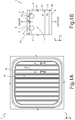
- Figure 1A shows, in top-plan view in a Cartesian (triaxial) reference system of axis X, Y, Z, a merged-PN-Schottky (MPS) device 1 of a known type.
- Figure 1B shows, in the same reference system, a lateral sectional view taken along line I-I, a portion of the MPS device 1.
- MPS merged-PN-Schottky
- the MPS device 1 includes: a substrate 3, of N-type SiC, having a first dopant concentration; a drift layer (epitaxially grown) 2, of N-type SiC, having a second dopant concentration lower than the first dopant concentration, extending on surface 3a of the substrate 3; a cathode terminal 6, of metal material, extending on surface 3b (opposite to surface 3a) of the substrate 3; an anode terminal 8, of metal material (anode metallization), extending on a top surface 2a the drift layer 2; a plurality of junction-barrier (JB) elements 9 in the drift layer 2, facing the top surface 2a of the drift layer 2, and including each a respective implanted region 9' of P-type and a ohmic contact 9" of metal material; and an edge termination region (guard ring) 10, in particular an implanted region of P-type, completely surrounding the junction-barrier (JB) elements 9.
- a substrate 3, of N-type SiC having a first dopant concentration
- Schottky diodes 12 are formed at the interface between the drift layer 2 and the metallization of the anode metallization 8.
- Schottky junctions metal-semiconductor
- portions of the drift layer 2 in direct electrical contact with respective portions of the anode metallization 8.
- the region of the MPS device 1 including the JB elements 9 and the Schottky diodes 12 is an active area 14 of the MPS device 1.
- MPS device 1 During use in the forward conducting state, due to the lower Schottky onset (about 0.7 V) than the PN onset (about 2.5 V), MPS device 1 functions as a Schottky diode at lower current densities (low on-state losses) and assumes the characteristic of a PN-diode at higher enough current densities.
- the asymmetric layout of Figure 1A induces a current-crowding effect in the active area 14 at the corners / rounded regions close to the intersection between the implanted regions 9' and the guard ring 10. Specifically, the corners in the active area 14 concentrate the current at a higher density than the rest of the active area 14.
- the bipolar conduction tends to be enabled first in these zones because of the higher voltage drop due to the higher current density and because of the higher temperature due to self-heating effect.
- Thermal runaway on very limited regions causes the formation of hot spots having a temperature that reaches high values, up to the material melting point, thus inducing a failure of the device or thermo-mechanical stresses that may ultimately lead to cracks in the die.
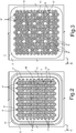
- FIG. 2 shows, in a top-plan view in the X, Y, Z reference system, an embodiment where the JB elements 9 are in the form of cells or dots, and include each an implanted region 9' having an hexagonal shape, with a respective ohmic contacts 9" formed within the implanted region 9'.
- the JB elements 9 are organized in a symmetrical array.
- the ohmic contacts are discontinuous.
- the Schottky diode 12 is formed by the drift layer 2 surrounding the JB elements 9 and the anode metallization 8 extending above the drift layer 2.
- FIG. 3 shows, in a top-plan view in the X, Y, Z reference system, an embodiment where both the Schottky diodes 12 and the JB elements 9 are in the form of cells or dots having an hexagonal shape. More in particular, each JB element 9 is completely surrounded by a respective Schottky diode 12; moreover, each Schottky diode 12 is completely surrounded (in top-plan view), and separated from ad adjacent Schottky diode 12, by a P+ region.
- the aim of the present invention is to provide a MPS diode with reduced current-crowding effect and a manufacturing method thereof, to overcome the drawbacks of the prior art.
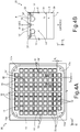
- Figure 4A shows, in the same reference system of axis X, Y, Z of Figures 1A-3 , a top-plan view (i.e., on XY plane) of a Merged-PN-Schottky (MPS) device 30 (in particular, a MPS diode), according to an embodiment of the present invention.
- Figure 4B shows, in the same reference system, a lateral sectional view taken along line IV-IV of Figure 4A .
- the anode metallization 8 is not shown, even if present, as apparent from the view of Figure 4B .
- each Schottky diode 32 of a plurality of Schottky diodes 32 includes a respective Schottky cell (or dot) 33 having, in top-plan view on XY plane, a squared shape; the Schottky cells 33 are arranged in a grid-like pattern, in particular forming a symmetric array of Schottky cells 33. Still more in particular, each Schottky cell 33 includes a superficial region of the drift layer 2 of N type of conductivity and N-doping concentration. The Schottky cells 33 are separated from one another, along X and Y directions, by implanted regions 19', of P conductivity type, extending in the drift layer 2.
- Each implanted region 19' separating one Schottky cell 33 from another, along both X and Y directions, is electrically connected to the other implanted regions 19', thus forming a continuous grid of implanted regions, which are therefore completely connected to one another.
- the implanted regions 19' form a set of squares, each square being one Schottky cell 33.
- Each Schottky cell 33 is thus completely surrounded, in top-plan view, by a respective one of the implanted regions 19'.
- Each implanted region 19' laterally surrounding one Schottky cell 33 is electrically connected to the other implanted regions 19' underneath the ohmic contacts 19" as shown in Figure 4B .
- the implanted regions 19' form a continuous grid extending under the grid of ohmic contacts 19".
- the implanted regions 19' include stripes along the X-axis direction that cross stripes along the Y-axis direction, to make a set of squares, each square being one Schottky cell 33.
- Each Schottky cell 33 is thus completely surrounded, in top-plan view, by the implanted regions 19'.
- each Schottky cell 33 is separated from an adjacent Schottky cell 33, along the X-axis direction, by a distance dx in the range 0.5pm-5pm; each Schottky cell 33 is separated from an adjacent Schottky cell 33, along the Y-axis direction, by a distance d Y in the range 0.5pm-5pm.
- distances d x and dy are equal to one another.
- the portion of the MPS device 30 where the Schottky cells 33 are formed is the active area 14 of the MPS device 30.
- a guard ring, or edge-termination region, 10, completely surrounding the active area 14, is also optionally present.
- the guard ring 10 extends as continuation of the implanted regions 19'.
- the implanted regions 19' and the guard ring 10 are connected to one another without any discontinuity. It is apparent that a continuous guard ring 10, completely surrounding the active area 14, may be omitted; in this case, the implanted regions 19' ends at the outer edges of the active area 14.
- the Schottky cells 33 form, with the anode metallization 8 extending above them and in direct electrical contact with them, the Schottky diodes 32 graphically represented in Figure 4B .
- the layout in top-plan view of the MPS device 30 is symmetric with respect to any line of symmetry passing through the centroid of the geometric shape delimited by the guard ring 10.
- the layout in top-plan view of the MPS device 30 is symmetric with respect to any line of symmetry passing through the centroid of the geometric figure delimited by the outer edges of the grid-like pattern (array) of Schottky cells 33 or, analogously, of the outer edges of the active area 14.
- guard ring 10 in Figure 4A has a quadrangular shape with rounded corners 10a.
- Schottky cells are not present at said rounded corners 10a.
- the guard ring 10 may be moved away from the active area 14, increasing the dimensions of the device 30 but avoiding the undesired current-crowding effect at the corners 10a).
- FIG. 5 shows an embodiment of an MPS device 30' where Schottky cells 33', which correspond in terms of functions to the Schottky cells 33 of MPS device 30, have each a quadrangular shape with rounded corners.
- Other elements of the MPS device 30' in common with elements of the MPS device 30 are identified with the same reference numerals and not further described.
- the cross sectional view of MPS device 30', taken along the line IV-IV in Figure 5 correspond to that of Figure 4B and therefore is not shown.
- FIG. 6 shows an embodiment of an MPS device 30" where Schottky cells 33", which correspond in terms of functions to the Schottky cells 33 of MPS device 30, have each a circular shape.
- Other elements of the MPS device 30" in common with elements of the MPS device 30 are identified with the same reference numerals and not further described.
- a method is also provided for manufacturing the MPS device 30 (reference can be made to Figures 7-11 ).
- the method disclosed herein can be also applied to manufacture the MPS device 30' and MPS device 30" of Figures 4 and 5 .
- Figures 7-11 illustrate, in lateral sectional view, steps of processing of a wafer 100 of semiconductor material.
- Figures 7-11 show the wafer 100 in the triaxial system of mutually orthogonal axes X, Y, Z of Figures 4A-4B .
- the wafer 100 comprises the substrate 3 of semiconductor material, in particular silicon carbide (SiC) having a first conductivity type (in this embodiment a doping of an N type), provided with a front side 3a and a back side 3b that are opposite to one another along the Z axis.
- the resistivity of the substrate 30 is, for example, comprised between 5 m ⁇ cm and 40 m ⁇ cm.
- the drift layer 2 On the front side 3a of the substrate 3, it is formed, for example by epitaxial growth, the drift layer 2, of silicon carbide having the first conductivity type (N) and having a concentration of dopants lower than that of the substrate 3, for example comprised between 1 ⁇ 10 14 and 5 ⁇ 10 16 atoms/cm 3 .
- the drift layer 2 is made of SiC, in particular 4H-SiC, but other polytypes may be used, such as 2H, 6H, 3C, and/or 15R.
- the substrate 3 and the drift layer 2 may be made of other semiconductor materials, for example GaN, GaAs, Ge.
- the drift layer 2 extends between a top side 2a and a bottom side 2b (the latter in direct contact with the front side 3a of the substrate 3).
- a hard mask 50 is formed, for example by deposition of photoresist, or TEOS, or other material.
- the hard mask 50 has a thickness of between 0.5 ⁇ m and 2 ⁇ m, or in any case a thickness such as to shield the implantation described hereinafter with reference to the same Figure 8 .
- the hard mask 34 thus formed extends in a region of the wafer 100 where, in subsequent steps, the active area 14 of the MPS device 30 will be formed.
- the hard mask 50 covers the regions of the top side 2a of drift layer 2 which will form the Schottky cells 33 and leaves exposed regions of the top side 2a of drift layer 2 which will form the implanted regions 19', identified with reference to Figures 4A and 4B .
- a step is now carried out of implantation of dopant species (e.g., boron or aluminium), which have the second conductivity type (here, P), exploiting the hard mask 50 (the implantation is indicated in the figure by arrows 52).
- dopant species e.g., boron or aluminium
- P the second conductivity type
- the guard ring 10 if present, is also formed.
- the step of Figure 8 comprises one or more implantations of dopant species, which have the second type of conductivity, with implantation energy comprised between 30 keV and 400 keV, and with doses of between 1 ⁇ 10 12 atoms/cm 2 and 1 ⁇ 10 15 atoms/cm 2 , in order to form the implanted regions 19' with dopant concentration higher than 1 ⁇ 10 18 atoms/cm 3 .
- the mask 50 is removed and a step of thermal annealing is carried out for diffusion and activation of the dopant species implanted in the step of Figure 8 .
- the thermal annealing is, for example, carried out at a temperature higher than 1600°C (e.g., between 1700 and 1900 °C, and in some cases even higher).
- the implanted regions 19' have a concentration of dopant species comprised between approximately 1 ⁇ 10 17 atoms/cm 3 and 1 ⁇ 10 20 atoms/cm 3 . Implanted regions 19' are thus formed.
- Schottky cells 33 are formed, that are the portions of the drift layer 2 which extends laterally to the implanted regions 19' or, in other words, the portions of the drift layer 2 of N-type masked during the implantation step of Figure 8 .
- Ohmic contacts 19" (e.g., of Nickel Silicide - Ni 2 Si) are then formed at each implanted region 19', thus concurring to the formation of respective JB elements 19. It is noted that implanted regions 19' visible in the cross sectional view are actually one uniform region, as it can be appreciated from the top view of Figure 4A . Accordingly, also ohmic contacts 19" are formed as one contact electrically connected to the implanted regions 19'. Therefore, the Schottky cells 33 are also separated from one another, along X and Y directions, by ohmic contacts 19" extending on the implanted regions 19'. As discussed above, the ohmic contacts 19" form a continuous grid overlying the grid of implanted regions and are therefore completely connected to one another.
- the ohmic contacts 19" form a continuous grid overlying the grid of implanted regions and are therefore completely connected to one another.
- An ohmic contact is also formed at the guard ring 10, electrically connected to the ohmic contacts 19".
- the formation of ohmic contacts 19" includes forming a hard mask of thin oxide (e.g., in the range of 100pm - 500pm); then photolithography and etching steps are performed to etch the regions where ohmic contacts 19" are to be formed; then, a deposition of metal material is carried out and a subsequent thermal treatment is performed (e.g., at a temperature in the range 900°C - 1100°C for a time interval in the range 10 minutes - 120 minutes).
- the metal thus deposited reacts with the superficial SiC material forming Ni2Si (i.e., the ohmic contact), while the metal in contact with the oxide does not react.
- a step of removal of the non-reacted metal is carried out and, then, a step of removal of the oxide metal is carried out.
- an interface layer 57 of metal material such as titanium, nickel, molybdenum, is deposited on the drift layer 2.
- the interface layer 57 is deposited via sputtering and has a thickness of between approximately 10 nm and 500 nm.
- the interface layer 57 extends in contact with the implanted regions 19' through the ohmic contacts 19", and with the exposed regions 33 of the drift layer 32 between the ohmic contacts 19" (i.e., the Schottky cells 33).
- the interface layer 57 contributes to the formation of a Schottky contact/Schottky barrier with the exposed regions 33 of the drift layer 32 and to the formation of junction-barrier (JB) elements with the implanted regions 19' through the ohmic contacts 19".
- JB junction-barrier
- the metal layer 58 is, for example, of aluminium or copper, and has a thickness of a few microns, for example between 1 and 10 ⁇ m.
- the ensemble constituted by the interface layer 57 and the metal layer 58 forms the anode metallization reference as 8 in Figure 4B .
- a plurality of metal-semiconductor junctions of a Schottky type 32 are thus formed between the anode metallization 8 and the regions of the drift layer 2 that have the first conductivity type (N), as represented in Figure 11 .
- the interface layer 57 is omitted, so that the anode metallization 8 coincides with the metal layer 58, which extends in direct contact with the drift layer 2.
- cathode contact 6 is formed on the back side 3b of the substrate 3, for example by depositing a layer of metal material adapted to form an ohmic contact with the substrate 3.
- the region of the drift layer 2 that extends along the axis Z between the Schottky junctions and the cathode is the active area 14 of the diode 30 (i.e., the region where drift of the electrical charges occurs).
- the guard ring 10 (not shown in figure 11 ) surrounds the active area 14.
- a plurality of MPS devices 30 are formed on the same wafer 100.
- a final step of die singulation is carried out to physically isolate one MPS device 30 from another.
- the MPS devices 30 of Figures 4A, 4B is thus formed.
- Figure 12 shows a further embodiment of the present invention, where the guard ring 10 has a quadrangular shape and Schottky cells 33 are also present at the inner corners of the guard ring 10.
Landscapes
- Electrodes Of Semiconductors (AREA)
Abstract
Description
- The present invention relates to a semiconductor MPS diode with reduced current-crowding effect and a manufacturing method thereof. In particular, the present invention relates to an electronic device based on silicon carbide, provided having an active area designed to minimise the crowding of electric current which flows during use from the anode to the cathode.
- As is known, semiconductor materials, which have a wide forbidden band gap, in particular, which have an energy value Eg of the forbidden band gap greater than 1.1 eV, low on-state resistance (RON), high value of thermal conductivity, high operating frequency, and high velocity saturation of charge carriers, are ideal for producing electronic components, such as diodes or transistors, in particular for power applications. A material having said characteristics, and designed to be used manufacturing electronic components, is silicon carbide (SiC). In particular, silicon carbide, in its different polytypes (e.g., 3C-SiC, 4H-SiC, 6H-SiC), is preferable to silicon as regards the properties listed previously.
- Electronic devices provided on a silicon-carbide substrate, as compared to similar devices provided on a silicon substrate, present numerous advantages, such as low output resistance in conduction, low leakage current, high working temperature, and high working frequencies. In particular, SiC Schottky diodes demonstrated superior switching performance, which renders SiC power devices especially favorable for high-frequency applications. Today's applications pose requirements on the electrical properties as well as on the long-term reliability of the devices.
-
Figure 1A shows, in top-plan view in a Cartesian (triaxial) reference system of axis X, Y, Z, a merged-PN-Schottky (MPS)device 1 of a known type.Figure 1B shows, in the same reference system, a lateral sectional view taken along line I-I, a portion of theMPS device 1. - With joint reference to
Figures 1A and 1B , theMPS device 1 includes: asubstrate 3, of N-type SiC, having a first dopant concentration; a drift layer (epitaxially grown) 2, of N-type SiC, having a second dopant concentration lower than the first dopant concentration, extending onsurface 3a of thesubstrate 3; acathode terminal 6, of metal material, extending onsurface 3b (opposite tosurface 3a) of thesubstrate 3; ananode terminal 8, of metal material (anode metallization), extending on atop surface 2a thedrift layer 2; a plurality of junction-barrier (JB)elements 9 in thedrift layer 2, facing thetop surface 2a of thedrift layer 2, and including each a respective implanted region 9' of P-type and aohmic contact 9" of metal material; and an edge termination region (guard ring) 10, in particular an implanted region of P-type, completely surrounding the junction-barrier (JB)elements 9. - Schottky
diodes 12 are formed at the interface between thedrift layer 2 and the metallization of theanode metallization 8. In particular, Schottky junctions (metal-semiconductor) are provided by portions of thedrift layer 2 in direct electrical contact with respective portions of theanode metallization 8. - The region of the
MPS device 1 including theJB elements 9 and the Schottky diodes 12 (i.e., the region contained within the guard ring 10) is anactive area 14 of theMPS device 1. - During use in the forward conducting state, due to the lower Schottky onset (about 0.7 V) than the PN onset (about 2.5 V),
MPS device 1 functions as a Schottky diode at lower current densities (low on-state losses) and assumes the characteristic of a PN-diode at higher enough current densities. The asymmetric layout ofFigure 1A induces a current-crowding effect in theactive area 14 at the corners / rounded regions close to the intersection between the implanted regions 9' and theguard ring 10. Specifically, the corners in theactive area 14 concentrate the current at a higher density than the rest of theactive area 14. At very high currents, the bipolar conduction tends to be enabled first in these zones because of the higher voltage drop due to the higher current density and because of the higher temperature due to self-heating effect. Thermal runaway on very limited regions, even at relatively small currents, causes the formation of hot spots having a temperature that reaches high values, up to the material melting point, thus inducing a failure of the device or thermo-mechanical stresses that may ultimately lead to cracks in the die. - To overcome the problems mentioned above, known solutions envisage the formation of the
JB elements 9 and/or of the Schottkydiodes 12 in a cell-like layout instead of a strip-like layout as inFigure 1A . Such known solutions are shown inFigures 2 and 3 , where the same reference numbers are used to indicate elements in common with the embodiment ofFigures 1A, 1B . -
Figure 2 shows, in a top-plan view in the X, Y, Z reference system, an embodiment where theJB elements 9 are in the form of cells or dots, and include each an implanted region 9' having an hexagonal shape, with arespective ohmic contacts 9" formed within the implanted region 9'. The JBelements 9 are organized in a symmetrical array. The ohmic contacts are discontinuous. The Schottkydiode 12 is formed by thedrift layer 2 surrounding theJB elements 9 and theanode metallization 8 extending above thedrift layer 2. -
Figure 3 shows, in a top-plan view in the X, Y, Z reference system, an embodiment where both the Schottkydiodes 12 and theJB elements 9 are in the form of cells or dots having an hexagonal shape. More in particular, eachJB element 9 is completely surrounded by a respective Schottkydiode 12; moreover, each Schottkydiode 12 is completely surrounded (in top-plan view), and separated from ad adjacent Schottkydiode 12, by a P+ region. - Even though the cell-like layouts of the solutions of
Figures 2 and 3 allow to avoid current crowding at device corners, the present Applicant found that a small local imbalance of current or temperature of one of theJB elements 9 or Schottkydiodes 12 may lead to a local electro-thermal runaway which may cause a failure of the MPS device. Moreover, the presence of several bipolar cells, even if provided withdedicated ohmic contacts 9", does not ensure a fast spreading of bipolar conduction current over the whole PN junction surface. - The aim of the present invention is to provide a MPS diode with reduced current-crowding effect and a manufacturing method thereof, to overcome the drawbacks of the prior art.
- According to the present invention, a MPS diode and a manufacturing method thereof are provided, as defined in the appended claims.
- For a better understanding of the present invention, preferred embodiments thereof are now described, purely by way of non-limiting example, with reference to the attached drawings, wherein:
-
Figures 1A and 1B show, in top-plan view and cross-sectional view respectively, a MPS (Merged-PN-Schottky) device according to a known embodiment; -
Figure 2 shows a MPS device according to a further known embodiment; -
Figure 3 shows a MPS device according to another known embodiment; -
Figures 4A and 4B show, in top-plan view and cross-sectional view respectively, a MPS (Merged-PN-Schottky) device according to an embodiment of the present invention; -
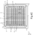
Figure 4C shows, in top-plan view, a MPS (Merged-PN-Schottky) device according to an embodiment alternative to that ofFigure 4A ; -
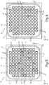
Figures 5 and 6 show, in top-plan view, respective layouts alternative to that ofFigure 4A ; -
Figures 7-11 show, in cross-sectional view, steps for manufacturing the MPS device ofFigures 4A, 4B ; and -
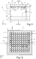
Figure 12 shows, in top-plan view, a MPS (Merged-PN-Schottky) device according to a further embodiment of the present invention. -
Figure 4A shows, in the same reference system of axis X, Y, Z ofFigures 1A-3 , a top-plan view (i.e., on XY plane) of a Merged-PN-Schottky (MPS) device 30 (in particular, a MPS diode), according to an embodiment of the present invention.Figure 4B shows, in the same reference system, a lateral sectional view taken along line IV-IV ofFigure 4A . To improve the understanding ofFigure 4A , theanode metallization 8 is not shown, even if present, as apparent from the view ofFigure 4B . - The lateral sectional view (i.e., on XZ plane) of
Figure 4B conforms substantially to that ofFigure 1B . Analogous elements are identified with the same reference numerals and not further described in detail. - However, when considering the top-plan view of
Figure 4A , the skilled person can appreciate that each Schottkydiode 32 of a plurality of Schottkydiodes 32 includes a respective Schottky cell (or dot) 33 having, in top-plan view on XY plane, a squared shape; the Schottkycells 33 are arranged in a grid-like pattern, in particular forming a symmetric array of Schottkycells 33. Still more in particular, each Schottkycell 33 includes a superficial region of thedrift layer 2 of N type of conductivity and N-doping concentration. The Schottkycells 33 are separated from one another, along X and Y directions, by implanted regions 19', of P conductivity type, extending in thedrift layer 2. Each implanted region 19' separating one Schottkycell 33 from another, along both X and Y directions, is electrically connected to the other implanted regions 19', thus forming a continuous grid of implanted regions, which are therefore completely connected to one another. In other words, the implanted regions 19' form a set of squares, each square being one Schottkycell 33. Each Schottkycell 33 is thus completely surrounded, in top-plan view, by a respective one of the implanted regions 19'. Each implanted region 19' laterally surrounding one Schottkycell 33 is electrically connected to the other implanted regions 19' underneath theohmic contacts 19" as shown inFigure 4B . As a result, the implanted regions 19' form a continuous grid extending under the grid ofohmic contacts 19". - In top-plan view, on the XY plane, the implanted regions 19' include stripes along the X-axis direction that cross stripes along the Y-axis direction, to make a set of squares, each square being one Schottky
cell 33. Each Schottkycell 33 is thus completely surrounded, in top-plan view, by the implanted regions 19'. - In an embodiment of the present invention, each Schottky
cell 33 is separated from an adjacent Schottkycell 33, along the X-axis direction, by a distance dx in the range 0.5pm-5pm; each Schottkycell 33 is separated from an adjacent Schottkycell 33, along the Y-axis direction, by a distance dY in the range 0.5pm-5pm. In particular, distances dx and dy are equal to one another. - The portion of the
MPS device 30 where the Schottkycells 33 are formed is theactive area 14 of theMPS device 30. - A guard ring, or edge-termination region, 10, completely surrounding the
active area 14, is also optionally present. In the embodiment shown, theguard ring 10 extends as continuation of the implanted regions 19'. In other words, the implanted regions 19' and theguard ring 10 are connected to one another without any discontinuity. It is apparent that acontinuous guard ring 10, completely surrounding theactive area 14, may be omitted; in this case, the implanted regions 19' ends at the outer edges of theactive area 14. - The Schottky
cells 33 form, with theanode metallization 8 extending above them and in direct electrical contact with them, the Schottkydiodes 32 graphically represented inFigure 4B . - According to an embodiment of the invention, the layout in top-plan view of the
MPS device 30 is symmetric with respect to any line of symmetry passing through the centroid of the geometric shape delimited by theguard ring 10. In the absence of aguard ring 10, the layout in top-plan view of theMPS device 30 is symmetric with respect to any line of symmetry passing through the centroid of the geometric figure delimited by the outer edges of the grid-like pattern (array) of Schottkycells 33 or, analogously, of the outer edges of theactive area 14. - It is noted that the
guard ring 10 inFigure 4A has a quadrangular shape withrounded corners 10a. In order to avoid a current crowding effect at said corners while at the same time shrinking the overall dimensions of the device, in the embodiment ofFigure 4A Schottky cells are not present at saidrounded corners 10a. - As shown in
Figure 4C , other embodiments, whereSchottky cells 33 are present at saidrounded corners 10a are possible (in this case, theguard ring 10 may be moved away from theactive area 14, increasing the dimensions of thedevice 30 but avoiding the undesired current-crowding effect at thecorners 10a). -
Figure 5 shows an embodiment of an MPS device 30' where Schottky cells 33', which correspond in terms of functions to theSchottky cells 33 ofMPS device 30, have each a quadrangular shape with rounded corners. Other elements of the MPS device 30' in common with elements of theMPS device 30 are identified with the same reference numerals and not further described. The cross sectional view of MPS device 30', taken along the line IV-IV inFigure 5 , correspond to that ofFigure 4B and therefore is not shown. -
Figure 6 shows an embodiment of anMPS device 30" whereSchottky cells 33", which correspond in terms of functions to theSchottky cells 33 ofMPS device 30, have each a circular shape. Other elements of theMPS device 30" in common with elements of theMPS device 30 are identified with the same reference numerals and not further described. - The cross sectional view of
MPS device 30", taken along the line IV-IV inFigure 6 , correspond to that ofFigure 4B and therefore is not shown. - According to the present invention, a method is also provided for manufacturing the MPS device 30 (reference can be made to
Figures 7-11 ). The method disclosed herein can be also applied to manufacture the MPS device 30' andMPS device 30" ofFigures 4 and5 . -
Figures 7-11 illustrate, in lateral sectional view, steps of processing of awafer 100 of semiconductor material.Figures 7-11 show thewafer 100 in the triaxial system of mutually orthogonal axes X, Y, Z ofFigures 4A-4B . - With reference to
Figure 7 , thewafer 100 comprises thesubstrate 3 of semiconductor material, in particular silicon carbide (SiC) having a first conductivity type (in this embodiment a doping of an N type), provided with afront side 3a and aback side 3b that are opposite to one another along the Z axis. The resistivity of thesubstrate 30 is, for example, comprised between 5 mΩ·cm and 40 mΩ·cm. - On the
front side 3a of thesubstrate 3, it is formed, for example by epitaxial growth, thedrift layer 2, of silicon carbide having the first conductivity type (N) and having a concentration of dopants lower than that of thesubstrate 3, for example comprised between 1·1014 and 5·1016 atoms/cm3. Thedrift layer 2 is made of SiC, in particular 4H-SiC, but other polytypes may be used, such as 2H, 6H, 3C, and/or 15R. - Alternatively, the
substrate 3 and thedrift layer 2 may be made of other semiconductor materials, for example GaN, GaAs, Ge. - The
drift layer 2 extends between atop side 2a and abottom side 2b (the latter in direct contact with thefront side 3a of the substrate 3). - Then,
Figure 8 , on thetop side 2a of thedrift layer 2 ahard mask 50 is formed, for example by deposition of photoresist, or TEOS, or other material. Thehard mask 50 has a thickness of between 0.5 µm and 2 µm, or in any case a thickness such as to shield the implantation described hereinafter with reference to the sameFigure 8 . The hard mask 34 thus formed extends in a region of thewafer 100 where, in subsequent steps, theactive area 14 of theMPS device 30 will be formed. - In top-plan view, on the XY plane, the
hard mask 50 covers the regions of thetop side 2a ofdrift layer 2 which will form theSchottky cells 33 and leaves exposed regions of thetop side 2a ofdrift layer 2 which will form the implanted regions 19', identified with reference toFigures 4A and 4B . - A step is now carried out of implantation of dopant species (e.g., boron or aluminium), which have the second conductivity type (here, P), exploiting the hard mask 50 (the implantation is indicated in the figure by arrows 52). The implanted regions 19' are thus formed.
- During the above implantation step, the
guard ring 10, if present, is also formed. - In one embodiment, the step of
Figure 8 comprises one or more implantations of dopant species, which have the second type of conductivity, with implantation energy comprised between 30 keV and 400 keV, and with doses of between 1·1012 atoms/cm2 and 1·1015 atoms/cm2, in order to form the implanted regions 19' with dopant concentration higher than 1·1018 atoms/cm3. - Next,
Figure 9 , themask 50 is removed and a step of thermal annealing is carried out for diffusion and activation of the dopant species implanted in the step ofFigure 8 . The thermal annealing is, for example, carried out at a temperature higher than 1600°C (e.g., between 1700 and 1900 °C, and in some cases even higher). Following upon thermal annealing, the implanted regions 19' have a concentration of dopant species comprised between approximately 1·1017 atoms/cm3 and 1·1020 atoms/cm3. Implanted regions 19' are thus formed. At the same time, alsoSchottky cells 33 are formed, that are the portions of thedrift layer 2 which extends laterally to the implanted regions 19' or, in other words, the portions of thedrift layer 2 of N-type masked during the implantation step ofFigure 8 . -
Ohmic contacts 19" (e.g., of Nickel Silicide - Ni2Si) are then formed at each implanted region 19', thus concurring to the formation ofrespective JB elements 19. It is noted that implanted regions 19' visible in the cross sectional view are actually one uniform region, as it can be appreciated from the top view ofFigure 4A . Accordingly, also ohmiccontacts 19" are formed as one contact electrically connected to the implanted regions 19'. Therefore, theSchottky cells 33 are also separated from one another, along X and Y directions, byohmic contacts 19" extending on the implanted regions 19'. As discussed above, theohmic contacts 19" form a continuous grid overlying the grid of implanted regions and are therefore completely connected to one another. - An ohmic contact is also formed at the
guard ring 10, electrically connected to theohmic contacts 19". - The formation of
ohmic contacts 19" includes forming a hard mask of thin oxide (e.g., in the range of 100pm - 500pm); then photolithography and etching steps are performed to etch the regions whereohmic contacts 19" are to be formed; then, a deposition of metal material is carried out and a subsequent thermal treatment is performed (e.g., at a temperature in the range 900°C - 1100°C for a time interval in therange 10 minutes - 120 minutes). The metal thus deposited reacts with the superficial SiC material forming Ni2Si (i.e., the ohmic contact), while the metal in contact with the oxide does not react. Then a step of removal of the non-reacted metal is carried out and, then, a step of removal of the oxide metal is carried out. - Then,
Figure 11 , a step of forming an anode metallization is carried out. - To this end, an
interface layer 57 of metal material, such as titanium, nickel, molybdenum, is deposited on thedrift layer 2. Theinterface layer 57 is deposited via sputtering and has a thickness of between approximately 10 nm and 500 nm. Theinterface layer 57 extends in contact with the implanted regions 19' through theohmic contacts 19", and with the exposedregions 33 of thedrift layer 32 between theohmic contacts 19" (i.e., the Schottky cells 33). In particular, theinterface layer 57 contributes to the formation of a Schottky contact/Schottky barrier with the exposedregions 33 of thedrift layer 32 and to the formation of junction-barrier (JB) elements with the implanted regions 19' through theohmic contacts 19". - Next, a
further metal layer 58 is formed on top of, and in direct contact with, theinterface layer 57. Themetal layer 58 is, for example, of aluminium or copper, and has a thickness of a few microns, for example between 1 and 10 µm. - The ensemble constituted by the
interface layer 57 and themetal layer 58 forms the anode metallization reference as 8 inFigure 4B . - A plurality of metal-semiconductor junctions of a
Schottky type 32 are thus formed between theanode metallization 8 and the regions of thedrift layer 2 that have the first conductivity type (N), as represented inFigure 11 . - In an alternative embodiment (not illustrated), the
interface layer 57 is omitted, so that theanode metallization 8 coincides with themetal layer 58, which extends in direct contact with thedrift layer 2. - Then,
cathode contact 6 is formed on theback side 3b of thesubstrate 3, for example by depositing a layer of metal material adapted to form an ohmic contact with thesubstrate 3. - The region of the
drift layer 2 that extends along the axis Z between the Schottky junctions and the cathode is theactive area 14 of the diode 30 (i.e., the region where drift of the electrical charges occurs). The guard ring 10 (not shown infigure 11 ) surrounds theactive area 14. - On the
same wafer 100, a plurality ofMPS devices 30 are formed. A final step of die singulation is carried out to physically isolate oneMPS device 30 from another. TheMPS devices 30 ofFigures 4A, 4B is thus formed. - From an examination of the characteristics of the invention provided according to the present disclosure the advantages that it affords are evident.
- Finally, it is clear that modifications and variations may be made to what has been described and illustrated herein, without thereby departing from the scope of the present invention, as defined in the annexed claims.
- In particular,
Figure 12 shows a further embodiment of the present invention, where theguard ring 10 has a quadrangular shape andSchottky cells 33 are also present at the inner corners of theguard ring 10.
Claims (16)
- A merged-PN-Schottky, MPS, diode (30), comprising:- a semiconductor substrate (3), having an N type conductivity and a first doping level;- a drift layer (2) of semiconductor material on the substrate (3), having a bottom surface (2b) which faces said substrate (3) and a top surface (2a) opposite to the bottom surface (2b), a N type conductivity and a second doping level lower than the first doping level;- a doped region (19') of P-type conductivity, extending in the drift layer (2) at the top surface (2a);- an ohmic contact (19"), in direct electrical contact with the doped region (19') at the top surface (2a);- a plurality of cells (33) of N-type conductivity and said second doping level, extending in the drift layer (2) within and through the doped region (19') and facing the top surface (2a);- an anode metallization (8) on said top surface (2a), in electrical contact with the doped region (19') through the ohmic contact (19") and in direct electrical contact with said cells (33), such as to form a junction-barrier, JB, diode with said doped region (19') and Schottky diodes with said cells (33),the JB diode and the Schottky diodes defining an active area (14) of the MPS diode (30),
characterized in that:the doped region (19') has, in top-plan view, a grid-shaped layout delimiting said plurality of cells (33),each cell (33) has a same geometry among quadrangular, quadrangular with rounded corners and circular, andsaid ohmic contact (19") extends at said doped region (19') with continuity along the grid-shaped layout. - The MPS diode (30) according to claim 1, wherein said grid-shaped layout is symmetric with respect to any axis of symmetry passing through a centroid of a geometrical shape defined by the outer edges of the active area(14).
- The MPS diode (30) according to claim 1 or 2, wherein the doped region (19') is formed by a plurality of first elongated regions, each having a respective main direction of extension parallel to a first axis (X), and by a respective plurality of second elongated regions, each having a respective main direction of extension parallel to a second axis (Y) orthogonal to the first axis (X),
said first and second elongated regions being designed to separate, in a top-plan view, each cell (33) from one another and to shape said cells (33) in such a way that each has, in the top-plan view, a same shape. - The MPS diode (30) according to claim 3, wherein said shape is one among quadrangular, quadrangular with rounded corners and circular.
- The MPS diode (30) according to claim 3 or 4, wherein said cells (33) form a quadrangular array of cells having rows parallel to said first axis (X) and columns parallel to said second axis (Y).
- The MPS diode (30) according to anyone of the preceding claims, wherein each cell (33) is a portion of the drift layer free from said doped region (19').
- The MPS diode (30) according to anyone of the preceding claims, wherein said substrate (3) and said drift layer (2) are both of silicon carbide or gallium nitride.
- The MPS diode (30) according to anyone of the preceding claims, wherein each one of said cells (33) has an area, at said top surface (2a), in the range 1µm2-100µm2.
- The MPS diode (30) according to anyone of the preceding claims, further comprising an edge-termination region, completely surrounding said active area (14) and extending as a prolongation of said doped region (19').
- A method of manufacturing a merged-PN-Schottky, MPS, diode (30), comprising the steps of:- forming a drift layer (2), of semiconductor material, on a substrate (3), the substrate (3) having a conductivity of N type and a first doping level, and the drift layer (2) having a conductivity of N type and a second doping level lower than the first doping level, wherein a top surface (2a) of the drift layer (2) is opposite to a bottom surface (2b) of the drift layer (2)which faces said substrate (3);- forming a doped region (19') of P-type conductivity, in the drift layer (2) at the top surface (2a);- forming an ohmic contact (19") in direct electrical contact with the doped region (19') at the top surface (2a);- forming a plurality of cells (33), of N-type conductivity and said second doping level, in the drift layer (2) within and through the doped region (19') and facing the top surface (2a);- forming an anode metallization (8), on the top surface (2a), in electrical contact with the doped region (19') through the ohmic contact (19") and in direct electrical contact with said cells (33), such as to form a junction-barrier diode with said doped region (19') and Schottky diodes with said cells (33),the JB diode and the Schottky diodes defining an active area (14) of the MPS diode (30),
characterized in that the steps of forming the doped region (19') and the cells (33) include implanting dopant species according to a grid-shaped layout, thus delimiting portions of the drift layer (2) that form respective cells (33),
and in that the implanting step is carried out with an implant mask shaped such that each cell (33) is formed having a same geometry among quadrangular, quadrangular with rounded corners and circular, and
and in that the step of forming said ohmic contact (19") includes depositing a metal material at said doped region (19') with continuity along the grid-shaped layout. - The method according to claim 10, wherein the step of forming the doped region (19') includes forming said grid-shaped layout which is symmetric with respect to any axis of symmetry passing through a centroid of a geometrical shape defined by the outer edges of the active area(14).
- The method according to claim 10 or 11, wherein the step of forming the doped region (19') includes forming a plurality of first elongated regions, each having a respective main direction of extension parallel to a first axis (X), and forming a respective plurality of second elongated regions, each having a respective main direction of extension parallel to a second axis (Y) orthogonal to the first axis (X),
said first and second elongated regions separating from one another each cell (33) of said plurality of cells (33) and shaping said cells (33) in such a way that, in a top-plan view, each cell (33) has a same shape. - The method according to claim 12, wherein said shape is one among quadrangular, quadrangular with rounded corners and circular.
- The method according to claim 12 or 13, wherein the step of forming said cells (33) includes forming a quadrangular array of cells having rows parallel to said first axis (X) and columns parallel to said second axis (Y).
- The method according to anyone of claims 10-14, wherein said substrate (3) and said drift layer (2) are both of silicon carbide or gallium nitride.
- The method according to anyone of claims 10-15, further comprising the step of forming an edge-termination region of P-type conductivity, completely surrounding said active area (14) and extending as a prolongation of said doped region (19'), wherein the step of forming the edge-termination is carried out contextually to the step of forming the doped region (19').
Applications Claiming Priority (1)
| Application Number | Priority Date | Filing Date | Title |
|---|---|---|---|
| IT201900004195 | 2019-03-22 |
Publications (3)
| Publication Number | Publication Date |
|---|---|
| EP3712962A1 true EP3712962A1 (en) | 2020-09-23 |
| EP3712962C0 EP3712962C0 (en) | 2023-06-07 |
| EP3712962B1 EP3712962B1 (en) | 2023-06-07 |
Family
ID=66776806
Family Applications (1)
| Application Number | Title | Priority Date | Filing Date |
|---|---|---|---|
| EP20164124.8A Active EP3712962B1 (en) | 2019-03-22 | 2020-03-19 | Semiconductor mps diode with reduced current-crowding effect and manufacturing method thereof |
Country Status (3)
| Country | Link |
|---|---|
| US (2) | US11417778B2 (en) |
| EP (1) | EP3712962B1 (en) |
| CN (2) | CN111725329B (en) |
Cited By (1)
| Publication number | Priority date | Publication date | Assignee | Title |
|---|---|---|---|---|
| CN114242767A (en) * | 2021-11-13 | 2022-03-25 | 深圳芯能半导体技术有限公司 | A kind of preparation method of MPS diode and MPS diode |
Families Citing this family (10)
| Publication number | Priority date | Publication date | Assignee | Title |
|---|---|---|---|---|
| EP3712962B1 (en) * | 2019-03-22 | 2023-06-07 | STMicroelectronics S.r.l. | Semiconductor mps diode with reduced current-crowding effect and manufacturing method thereof |
| IT202000004696A1 (en) | 2020-03-05 | 2021-09-05 | St Microelectronics Srl | MANUFACTURING METHOD OF AN ELECTRONIC DEVICE IN SiC WITH REDUCED HANDLING PHASES, AND ELECTRONIC DEVICE IN SiC |
| IT202000008179A1 (en) | 2020-04-17 | 2021-10-17 | St Microelectronics Srl | FORMATION OF OHMIC CONTACTS IN A SIC BASED ELECTRONIC DEVICE, AND ELECTRONIC DEVICE |
| IT202000008167A1 (en) | 2020-04-17 | 2021-10-17 | St Microelectronics Srl | DRUG ACTIVATION AND FORMATION OF OHMIC CONTACT IN AN ELECTRONIC DEVICE IN SIC, AND ELECTRONIC DEVICE IN SIC |
| IT202000015100A1 (en) | 2020-06-23 | 2021-12-23 | St Microelectronics Srl | METHOD OF MANUFACTURING SIC-BASED UV RADIATION DETECTOR AND SIC-BASED UV RADIATION DETECTOR |
| IT202100002333A1 (en) * | 2021-02-03 | 2022-08-03 | St Microelectronics Srl | JBS DEVICE WITH IMPROVED ELECTRICAL PERFORMANCE, AND JBS DEVICE MANUFACTURING PROCESS |
| CN113990934B (en) * | 2021-10-29 | 2023-07-28 | 西安微电子技术研究所 | A kind of SiC JBS cell structure and preparation method |
| CN116387313B (en) * | 2023-04-28 | 2026-05-05 | 深圳市至信微电子有限公司 | A silicon carbide Schottky diode chip, circuit board assembly and electronic device |
| US12588302B2 (en) | 2023-05-16 | 2026-03-24 | Omnivision Technologies, Inc. | Backside deep trench isolation structure for leakage suppression |
| IT202300019941A1 (en) * | 2023-09-27 | 2025-03-27 | St Microelectronics Int Nv | FORMATION OF A SCHOTTKY CONTACT IN AN ELECTRONIC DEVICE, SUCH AS A JBS OR MPS DIODE, AND ELECTRONIC DEVICE WITH A SCHOTTKY CONTACT |
Citations (5)
| Publication number | Priority date | Publication date | Assignee | Title |
|---|---|---|---|---|
| US20080277668A1 (en) * | 2007-05-10 | 2008-11-13 | Denso Corporation | SIS semiconductor having junction barrier schottky device |
| JP2011142355A (en) * | 2011-04-21 | 2011-07-21 | Sumitomo Electric Ind Ltd | Rectifying element |
| US20130105819A1 (en) * | 2011-10-28 | 2013-05-02 | Hitachi, Ltd. | Semiconductor device |
| US9455326B2 (en) * | 2012-02-15 | 2016-09-27 | Fuji Electric Co., Ltd. | Wide bandgap semiconductor device |
| US20180190651A1 (en) * | 2017-01-04 | 2018-07-05 | Infineon Technologies Ag | Semiconductor Device and Corresponding Manufacturing Method |
Family Cites Families (11)
| Publication number | Priority date | Publication date | Assignee | Title |
|---|---|---|---|---|
| JP2001508946A (en) * | 1997-01-20 | 2001-07-03 | エービービー リサーチ リミテッド | Schottky diode using SiC and method of manufacturing the same |
| US6524900B2 (en) * | 2001-07-25 | 2003-02-25 | Abb Research, Ltd | Method concerning a junction barrier Schottky diode, such a diode and use thereof |
| JP2006352006A (en) * | 2005-06-20 | 2006-12-28 | Sumitomo Electric Ind Ltd | Rectifying element and manufacturing method thereof |
| JP2009158519A (en) * | 2007-12-25 | 2009-07-16 | Toyota Motor Corp | Semiconductor device and manufacturing method thereof |
| EP2154726A3 (en) * | 2008-08-14 | 2010-05-26 | Acreo AB | A method for producing a JBS diode |
| JP6206862B2 (en) * | 2012-05-31 | 2017-10-04 | 富士電機株式会社 | Silicon carbide semiconductor device and method for manufacturing silicon carbide semiconductor device |
| US10181532B2 (en) * | 2013-03-15 | 2019-01-15 | Cree, Inc. | Low loss electronic devices having increased doping for reduced resistance and methods of forming the same |
| JP6356592B2 (en) * | 2014-12-17 | 2018-07-11 | トヨタ自動車株式会社 | Schottky barrier diode and manufacturing method thereof |
| JP6267108B2 (en) * | 2014-12-22 | 2018-01-24 | トヨタ自動車株式会社 | Schottky barrier diode and manufacturing method thereof |
| CN109065620B (en) * | 2018-08-22 | 2023-10-13 | 江苏中科君芯科技有限公司 | An IGBT device with low Miller capacitance |
| EP3712962B1 (en) * | 2019-03-22 | 2023-06-07 | STMicroelectronics S.r.l. | Semiconductor mps diode with reduced current-crowding effect and manufacturing method thereof |
-
2020
- 2020-03-19 EP EP20164124.8A patent/EP3712962B1/en active Active
- 2020-03-20 CN CN202010203662.4A patent/CN111725329B/en active Active
- 2020-03-20 US US16/825,214 patent/US11417778B2/en active Active
- 2020-03-20 CN CN202020364341.8U patent/CN212365972U/en not_active Withdrawn - After Issue
-
2022
- 2022-08-10 US US17/818,926 patent/US12094985B2/en active Active
Patent Citations (5)
| Publication number | Priority date | Publication date | Assignee | Title |
|---|---|---|---|---|
| US20080277668A1 (en) * | 2007-05-10 | 2008-11-13 | Denso Corporation | SIS semiconductor having junction barrier schottky device |
| JP2011142355A (en) * | 2011-04-21 | 2011-07-21 | Sumitomo Electric Ind Ltd | Rectifying element |
| US20130105819A1 (en) * | 2011-10-28 | 2013-05-02 | Hitachi, Ltd. | Semiconductor device |
| US9455326B2 (en) * | 2012-02-15 | 2016-09-27 | Fuji Electric Co., Ltd. | Wide bandgap semiconductor device |
| US20180190651A1 (en) * | 2017-01-04 | 2018-07-05 | Infineon Technologies Ag | Semiconductor Device and Corresponding Manufacturing Method |
Cited By (1)
| Publication number | Priority date | Publication date | Assignee | Title |
|---|---|---|---|---|
| CN114242767A (en) * | 2021-11-13 | 2022-03-25 | 深圳芯能半导体技术有限公司 | A kind of preparation method of MPS diode and MPS diode |
Also Published As
| Publication number | Publication date |
|---|---|
| US20200303564A1 (en) | 2020-09-24 |
| US20220384662A1 (en) | 2022-12-01 |
| EP3712962C0 (en) | 2023-06-07 |
| US11417778B2 (en) | 2022-08-16 |
| CN212365972U (en) | 2021-01-15 |
| EP3712962B1 (en) | 2023-06-07 |
| US12094985B2 (en) | 2024-09-17 |
| CN111725329A (en) | 2020-09-29 |
| CN111725329B (en) | 2025-09-02 |
Similar Documents
| Publication | Publication Date | Title |
|---|---|---|
| US12094985B2 (en) | Semiconductor MPS diode with reduced current-crowding effect and manufacturing method thereof | |
| JP5559530B2 (en) | Junction barrier Schottky rectifier and manufacturing method thereof | |
| KR101774124B1 (en) | Semiconductor devices and method for fabricating the same | |
| EP2754181B1 (en) | Schottky diode | |
| JP6425659B2 (en) | Schottky diode and method of manufacturing Schottky diode | |
| CN101223647B (en) | SiC Junction Barrier Schottky Diodes with Suppressed Minority Carrier Injection | |
| EP2754179B1 (en) | Schottky diode employing recesses for elements of junction barrier array | |
| US9029944B2 (en) | Super junction semiconductor device comprising implanted zones | |
| JP7782978B2 (en) | Wide bandgap semiconductor electronic device with JBS diode having improved electrical characteristics and method for fabricating same | |
| US20220246771A1 (en) | Vertical conduction electronic device comprising a jbs diode and manufacturing process thereof | |
| WO2024073688A2 (en) | Silicon carbide device with single metallization process for ohmic and schottky contacts | |
| CN217405436U (en) | Junction barrier schottky device and junction barrier schottky apparatus | |
| CN216597601U (en) | Merged Pin Schottky device and electronic device | |
| CN216413051U (en) | semiconductor equipment | |
| CN113990955B (en) | Silicon carbide diode with reduced voltage drop and method of making same | |
| WO2019053204A1 (en) | Feeder design with high current capability | |
| WO2012054032A1 (en) | Embedded wells merged pn/schottky diode | |
| CN116936643A (en) | Merged PiN Schottky (MPS) diode and method of fabrication |
Legal Events
| Date | Code | Title | Description |
|---|---|---|---|
| PUAI | Public reference made under article 153(3) epc to a published international application that has entered the european phase |
Free format text: ORIGINAL CODE: 0009012 |
|
| STAA | Information on the status of an ep patent application or granted ep patent |
Free format text: STATUS: THE APPLICATION HAS BEEN PUBLISHED |
|
| AK | Designated contracting states |
Kind code of ref document: A1 Designated state(s): AL AT BE BG CH CY CZ DE DK EE ES FI FR GB GR HR HU IE IS IT LI LT LU LV MC MK MT NL NO PL PT RO RS SE SI SK SM TR |
|
| AX | Request for extension of the european patent |
Extension state: BA ME |
|
| STAA | Information on the status of an ep patent application or granted ep patent |
Free format text: STATUS: REQUEST FOR EXAMINATION WAS MADE |
|
| 17P | Request for examination filed |
Effective date: 20210125 |
|
| RBV | Designated contracting states (corrected) |
Designated state(s): AL AT BE BG CH CY CZ DE DK EE ES FI FR GB GR HR HU IE IS IT LI LT LU LV MC MK MT NL NO PL PT RO RS SE SI SK SM TR |
|
| STAA | Information on the status of an ep patent application or granted ep patent |
Free format text: STATUS: EXAMINATION IS IN PROGRESS |
|
| 17Q | First examination report despatched |
Effective date: 20210628 |
|
| GRAP | Despatch of communication of intention to grant a patent |
Free format text: ORIGINAL CODE: EPIDOSNIGR1 |
|
| STAA | Information on the status of an ep patent application or granted ep patent |
Free format text: STATUS: GRANT OF PATENT IS INTENDED |
|
| RIC1 | Information provided on ipc code assigned before grant |
Ipc: H01L 29/20 20060101ALN20221108BHEP Ipc: H01L 21/329 20060101ALI20221108BHEP Ipc: H01L 29/16 20060101ALI20221108BHEP Ipc: H01L 29/06 20060101ALI20221108BHEP Ipc: H01L 29/872 20060101AFI20221108BHEP |
|
| INTG | Intention to grant announced |
Effective date: 20221208 |
|
| RIC1 | Information provided on ipc code assigned before grant |
Ipc: H01L 29/20 20060101ALN20221128BHEP Ipc: H01L 21/329 20060101ALI20221128BHEP Ipc: H01L 29/16 20060101ALI20221128BHEP Ipc: H01L 29/06 20060101ALI20221128BHEP Ipc: H01L 29/872 20060101AFI20221128BHEP |
|
| GRAS | Grant fee paid |
Free format text: ORIGINAL CODE: EPIDOSNIGR3 |
|
| GRAA | (expected) grant |
Free format text: ORIGINAL CODE: 0009210 |
|
| STAA | Information on the status of an ep patent application or granted ep patent |
Free format text: STATUS: THE PATENT HAS BEEN GRANTED |
|
| AK | Designated contracting states |
Kind code of ref document: B1 Designated state(s): AL AT BE BG CH CY CZ DE DK EE ES FI FR GB GR HR HU IE IS IT LI LT LU LV MC MK MT NL NO PL PT RO RS SE SI SK SM TR |
|
| REG | Reference to a national code |
Ref country code: GB Ref legal event code: FG4D |
|
| REG | Reference to a national code |
Ref country code: CH Ref legal event code: EP Ref country code: AT Ref legal event code: REF Ref document number: 1577566 Country of ref document: AT Kind code of ref document: T Effective date: 20230615 Ref country code: DE Ref legal event code: R096 Ref document number: 602020011490 Country of ref document: DE |
|
| U01 | Request for unitary effect filed |
Effective date: 20230629 |
|
| U07 | Unitary effect registered |
Designated state(s): AT BE BG DE DK EE FI FR IT LT LU LV MT NL PT SE SI Effective date: 20230710 |
|
| REG | Reference to a national code |
Ref country code: LT Ref legal event code: MG9D |
|
| PG25 | Lapsed in a contracting state [announced via postgrant information from national office to epo] |
Ref country code: NO Free format text: LAPSE BECAUSE OF FAILURE TO SUBMIT A TRANSLATION OF THE DESCRIPTION OR TO PAY THE FEE WITHIN THE PRESCRIBED TIME-LIMIT Effective date: 20230907 Ref country code: ES Free format text: LAPSE BECAUSE OF FAILURE TO SUBMIT A TRANSLATION OF THE DESCRIPTION OR TO PAY THE FEE WITHIN THE PRESCRIBED TIME-LIMIT Effective date: 20230607 |
|
| PG25 | Lapsed in a contracting state [announced via postgrant information from national office to epo] |
Ref country code: RS Free format text: LAPSE BECAUSE OF FAILURE TO SUBMIT A TRANSLATION OF THE DESCRIPTION OR TO PAY THE FEE WITHIN THE PRESCRIBED TIME-LIMIT Effective date: 20230607 Ref country code: HR Free format text: LAPSE BECAUSE OF FAILURE TO SUBMIT A TRANSLATION OF THE DESCRIPTION OR TO PAY THE FEE WITHIN THE PRESCRIBED TIME-LIMIT Effective date: 20230607 Ref country code: GR Free format text: LAPSE BECAUSE OF FAILURE TO SUBMIT A TRANSLATION OF THE DESCRIPTION OR TO PAY THE FEE WITHIN THE PRESCRIBED TIME-LIMIT Effective date: 20230908 |
|
| PG25 | Lapsed in a contracting state [announced via postgrant information from national office to epo] |
Ref country code: SK Free format text: LAPSE BECAUSE OF FAILURE TO SUBMIT A TRANSLATION OF THE DESCRIPTION OR TO PAY THE FEE WITHIN THE PRESCRIBED TIME-LIMIT Effective date: 20230607 |
|
| PG25 | Lapsed in a contracting state [announced via postgrant information from national office to epo] |
Ref country code: IS Free format text: LAPSE BECAUSE OF FAILURE TO SUBMIT A TRANSLATION OF THE DESCRIPTION OR TO PAY THE FEE WITHIN THE PRESCRIBED TIME-LIMIT Effective date: 20231007 |
|
| PG25 | Lapsed in a contracting state [announced via postgrant information from national office to epo] |
Ref country code: SM Free format text: LAPSE BECAUSE OF FAILURE TO SUBMIT A TRANSLATION OF THE DESCRIPTION OR TO PAY THE FEE WITHIN THE PRESCRIBED TIME-LIMIT Effective date: 20230607 Ref country code: SK Free format text: LAPSE BECAUSE OF FAILURE TO SUBMIT A TRANSLATION OF THE DESCRIPTION OR TO PAY THE FEE WITHIN THE PRESCRIBED TIME-LIMIT Effective date: 20230607 Ref country code: RO Free format text: LAPSE BECAUSE OF FAILURE TO SUBMIT A TRANSLATION OF THE DESCRIPTION OR TO PAY THE FEE WITHIN THE PRESCRIBED TIME-LIMIT Effective date: 20230607 Ref country code: IS Free format text: LAPSE BECAUSE OF FAILURE TO SUBMIT A TRANSLATION OF THE DESCRIPTION OR TO PAY THE FEE WITHIN THE PRESCRIBED TIME-LIMIT Effective date: 20231007 Ref country code: CZ Free format text: LAPSE BECAUSE OF FAILURE TO SUBMIT A TRANSLATION OF THE DESCRIPTION OR TO PAY THE FEE WITHIN THE PRESCRIBED TIME-LIMIT Effective date: 20230607 |
|
| PG25 | Lapsed in a contracting state [announced via postgrant information from national office to epo] |
Ref country code: PL Free format text: LAPSE BECAUSE OF FAILURE TO SUBMIT A TRANSLATION OF THE DESCRIPTION OR TO PAY THE FEE WITHIN THE PRESCRIBED TIME-LIMIT Effective date: 20230607 |
|
| REG | Reference to a national code |
Ref country code: DE Ref legal event code: R097 Ref document number: 602020011490 Country of ref document: DE |
|
| U20 | Renewal fee for the european patent with unitary effect paid |
Year of fee payment: 5 Effective date: 20240220 |
|
| PLBE | No opposition filed within time limit |
Free format text: ORIGINAL CODE: 0009261 |
|
| STAA | Information on the status of an ep patent application or granted ep patent |
Free format text: STATUS: NO OPPOSITION FILED WITHIN TIME LIMIT |
|
| 26N | No opposition filed |
Effective date: 20240308 |
|
| REG | Reference to a national code |
Ref country code: CH Ref legal event code: PL |
|
| PG25 | Lapsed in a contracting state [announced via postgrant information from national office to epo] |
Ref country code: MC Free format text: LAPSE BECAUSE OF FAILURE TO SUBMIT A TRANSLATION OF THE DESCRIPTION OR TO PAY THE FEE WITHIN THE PRESCRIBED TIME-LIMIT Effective date: 20230607 |
|
| GBPC | Gb: european patent ceased through non-payment of renewal fee |
Effective date: 20240319 |
|
| PG25 | Lapsed in a contracting state [announced via postgrant information from national office to epo] |
Ref country code: MC Free format text: LAPSE BECAUSE OF FAILURE TO SUBMIT A TRANSLATION OF THE DESCRIPTION OR TO PAY THE FEE WITHIN THE PRESCRIBED TIME-LIMIT Effective date: 20230607 |
|
| PG25 | Lapsed in a contracting state [announced via postgrant information from national office to epo] |
Ref country code: GB Free format text: LAPSE BECAUSE OF NON-PAYMENT OF DUE FEES Effective date: 20240319 |
|
| PG25 | Lapsed in a contracting state [announced via postgrant information from national office to epo] |
Ref country code: IE Free format text: LAPSE BECAUSE OF NON-PAYMENT OF DUE FEES Effective date: 20240319 |
|
| PG25 | Lapsed in a contracting state [announced via postgrant information from national office to epo] |
Ref country code: IE Free format text: LAPSE BECAUSE OF NON-PAYMENT OF DUE FEES Effective date: 20240319 Ref country code: GB Free format text: LAPSE BECAUSE OF NON-PAYMENT OF DUE FEES Effective date: 20240319 Ref country code: CH Free format text: LAPSE BECAUSE OF NON-PAYMENT OF DUE FEES Effective date: 20240331 |
|
| U20 | Renewal fee for the european patent with unitary effect paid |
Year of fee payment: 6 Effective date: 20250210 |
|
| PG25 | Lapsed in a contracting state [announced via postgrant information from national office to epo] |
Ref country code: CY Free format text: LAPSE BECAUSE OF FAILURE TO SUBMIT A TRANSLATION OF THE DESCRIPTION OR TO PAY THE FEE WITHIN THE PRESCRIBED TIME-LIMIT; INVALID AB INITIO Effective date: 20200319 |
|
| PG25 | Lapsed in a contracting state [announced via postgrant information from national office to epo] |
Ref country code: HU Free format text: LAPSE BECAUSE OF FAILURE TO SUBMIT A TRANSLATION OF THE DESCRIPTION OR TO PAY THE FEE WITHIN THE PRESCRIBED TIME-LIMIT; INVALID AB INITIO Effective date: 20200319 |
|
| PG25 | Lapsed in a contracting state [announced via postgrant information from national office to epo] |
Ref country code: TR Free format text: LAPSE BECAUSE OF FAILURE TO SUBMIT A TRANSLATION OF THE DESCRIPTION OR TO PAY THE FEE WITHIN THE PRESCRIBED TIME-LIMIT Effective date: 20230607 |
|
| U20 | Renewal fee for the european patent with unitary effect paid |
Year of fee payment: 7 Effective date: 20260219 |