EP3712934A1 - Package structure and forming method of the same - Google Patents
Package structure and forming method of the same Download PDFInfo
- Publication number
- EP3712934A1 EP3712934A1 EP19218103.0A EP19218103A EP3712934A1 EP 3712934 A1 EP3712934 A1 EP 3712934A1 EP 19218103 A EP19218103 A EP 19218103A EP 3712934 A1 EP3712934 A1 EP 3712934A1
- Authority
- EP
- European Patent Office
- Prior art keywords
- conduction layer
- chip
- package structure
- lead frame
- layer
- Prior art date
- Legal status (The legal status is an assumption and is not a legal conclusion. Google has not performed a legal analysis and makes no representation as to the accuracy of the status listed.)
- Withdrawn
Links
Images







Classifications
-
- H—ELECTRICITY
- H10—SEMICONDUCTOR DEVICES; ELECTRIC SOLID-STATE DEVICES NOT OTHERWISE PROVIDED FOR
- H10W—GENERIC PACKAGES, INTERCONNECTIONS, CONNECTORS OR OTHER CONSTRUCTIONAL DETAILS OF DEVICES COVERED BY CLASS H10
- H10W40/00—Arrangements for thermal protection or thermal control
- H10W40/70—Fillings or auxiliary members in containers or in encapsulations for thermal protection or control
- H10W40/77—Auxiliary members characterised by their shape
- H10W40/778—Auxiliary members characterised by their shape in encapsulations
-
- H—ELECTRICITY
- H10—SEMICONDUCTOR DEVICES; ELECTRIC SOLID-STATE DEVICES NOT OTHERWISE PROVIDED FOR
- H10W—GENERIC PACKAGES, INTERCONNECTIONS, CONNECTORS OR OTHER CONSTRUCTIONAL DETAILS OF DEVICES COVERED BY CLASS H10
- H10W74/00—Encapsulations, e.g. protective coatings
- H10W74/10—Encapsulations, e.g. protective coatings characterised by their shape or disposition
- H10W74/111—Encapsulations, e.g. protective coatings characterised by their shape or disposition the semiconductor body being completely enclosed
- H10W74/114—Encapsulations, e.g. protective coatings characterised by their shape or disposition the semiconductor body being completely enclosed by a substrate and the encapsulations
- H10W74/117—Encapsulations, e.g. protective coatings characterised by their shape or disposition the semiconductor body being completely enclosed by a substrate and the encapsulations the substrate having spherical bumps for external connection
-
- H—ELECTRICITY
- H10—SEMICONDUCTOR DEVICES; ELECTRIC SOLID-STATE DEVICES NOT OTHERWISE PROVIDED FOR
- H10W—GENERIC PACKAGES, INTERCONNECTIONS, CONNECTORS OR OTHER CONSTRUCTIONAL DETAILS OF DEVICES COVERED BY CLASS H10
- H10W70/00—Package substrates; Interposers; Redistribution layers [RDL]
- H10W70/01—Manufacture or treatment
- H10W70/05—Manufacture or treatment of insulating or insulated package substrates, or of interposers, or of redistribution layers
-
- H—ELECTRICITY
- H10—SEMICONDUCTOR DEVICES; ELECTRIC SOLID-STATE DEVICES NOT OTHERWISE PROVIDED FOR
- H10W—GENERIC PACKAGES, INTERCONNECTIONS, CONNECTORS OR OTHER CONSTRUCTIONAL DETAILS OF DEVICES COVERED BY CLASS H10
- H10W70/00—Package substrates; Interposers; Redistribution layers [RDL]
- H10W70/40—Leadframes
- H10W70/421—Shapes or dispositions
- H10W70/424—Cross-sectional shapes
-
- H—ELECTRICITY
- H10—SEMICONDUCTOR DEVICES; ELECTRIC SOLID-STATE DEVICES NOT OTHERWISE PROVIDED FOR
- H10W—GENERIC PACKAGES, INTERCONNECTIONS, CONNECTORS OR OTHER CONSTRUCTIONAL DETAILS OF DEVICES COVERED BY CLASS H10
- H10W70/00—Package substrates; Interposers; Redistribution layers [RDL]
- H10W70/40—Leadframes
- H10W70/451—Multilayered leadframes
-
- H—ELECTRICITY
- H10—SEMICONDUCTOR DEVICES; ELECTRIC SOLID-STATE DEVICES NOT OTHERWISE PROVIDED FOR
- H10W—GENERIC PACKAGES, INTERCONNECTIONS, CONNECTORS OR OTHER CONSTRUCTIONAL DETAILS OF DEVICES COVERED BY CLASS H10
- H10W70/00—Package substrates; Interposers; Redistribution layers [RDL]
- H10W70/40—Leadframes
- H10W70/464—Additional interconnections in combination with leadframes
-
- H—ELECTRICITY
- H10—SEMICONDUCTOR DEVICES; ELECTRIC SOLID-STATE DEVICES NOT OTHERWISE PROVIDED FOR
- H10W—GENERIC PACKAGES, INTERCONNECTIONS, CONNECTORS OR OTHER CONSTRUCTIONAL DETAILS OF DEVICES COVERED BY CLASS H10
- H10W70/00—Package substrates; Interposers; Redistribution layers [RDL]
- H10W70/40—Leadframes
- H10W70/464—Additional interconnections in combination with leadframes
- H10W70/466—Tape carriers or flat leads
-
- H—ELECTRICITY
- H10—SEMICONDUCTOR DEVICES; ELECTRIC SOLID-STATE DEVICES NOT OTHERWISE PROVIDED FOR
- H10W—GENERIC PACKAGES, INTERCONNECTIONS, CONNECTORS OR OTHER CONSTRUCTIONAL DETAILS OF DEVICES COVERED BY CLASS H10
- H10W70/00—Package substrates; Interposers; Redistribution layers [RDL]
- H10W70/40—Leadframes
- H10W70/464—Additional interconnections in combination with leadframes
- H10W70/468—Circuit boards
-
- H—ELECTRICITY
- H10—SEMICONDUCTOR DEVICES; ELECTRIC SOLID-STATE DEVICES NOT OTHERWISE PROVIDED FOR
- H10W—GENERIC PACKAGES, INTERCONNECTIONS, CONNECTORS OR OTHER CONSTRUCTIONAL DETAILS OF DEVICES COVERED BY CLASS H10
- H10W70/00—Package substrates; Interposers; Redistribution layers [RDL]
- H10W70/40—Leadframes
- H10W70/481—Leadframes for devices being provided for in groups H10D8/00 - H10D48/00
-
- H—ELECTRICITY
- H10—SEMICONDUCTOR DEVICES; ELECTRIC SOLID-STATE DEVICES NOT OTHERWISE PROVIDED FOR
- H10W—GENERIC PACKAGES, INTERCONNECTIONS, CONNECTORS OR OTHER CONSTRUCTIONAL DETAILS OF DEVICES COVERED BY CLASS H10
- H10W70/00—Package substrates; Interposers; Redistribution layers [RDL]
- H10W70/60—Insulating or insulated package substrates; Interposers; Redistribution layers
- H10W70/611—Insulating or insulated package substrates; Interposers; Redistribution layers for connecting multiple chips together
-
- H—ELECTRICITY
- H10—SEMICONDUCTOR DEVICES; ELECTRIC SOLID-STATE DEVICES NOT OTHERWISE PROVIDED FOR
- H10W—GENERIC PACKAGES, INTERCONNECTIONS, CONNECTORS OR OTHER CONSTRUCTIONAL DETAILS OF DEVICES COVERED BY CLASS H10
- H10W70/00—Package substrates; Interposers; Redistribution layers [RDL]
- H10W70/60—Insulating or insulated package substrates; Interposers; Redistribution layers
- H10W70/67—Insulating or insulated package substrates; Interposers; Redistribution layers characterised by their insulating layers or insulating parts
- H10W70/68—Shapes or dispositions thereof
- H10W70/685—Shapes or dispositions thereof comprising multiple insulating layers
-
- H—ELECTRICITY
- H10—SEMICONDUCTOR DEVICES; ELECTRIC SOLID-STATE DEVICES NOT OTHERWISE PROVIDED FOR
- H10W—GENERIC PACKAGES, INTERCONNECTIONS, CONNECTORS OR OTHER CONSTRUCTIONAL DETAILS OF DEVICES COVERED BY CLASS H10
- H10W74/00—Encapsulations, e.g. protective coatings
- H10W74/10—Encapsulations, e.g. protective coatings characterised by their shape or disposition
- H10W74/111—Encapsulations, e.g. protective coatings characterised by their shape or disposition the semiconductor body being completely enclosed
- H10W74/129—Encapsulations, e.g. protective coatings characterised by their shape or disposition the semiconductor body being completely enclosed forming a chip-scale package [CSP]
-
- H—ELECTRICITY
- H10—SEMICONDUCTOR DEVICES; ELECTRIC SOLID-STATE DEVICES NOT OTHERWISE PROVIDED FOR
- H10W—GENERIC PACKAGES, INTERCONNECTIONS, CONNECTORS OR OTHER CONSTRUCTIONAL DETAILS OF DEVICES COVERED BY CLASS H10
- H10W90/00—Package configurations
-
- H—ELECTRICITY
- H10—SEMICONDUCTOR DEVICES; ELECTRIC SOLID-STATE DEVICES NOT OTHERWISE PROVIDED FOR
- H10W—GENERIC PACKAGES, INTERCONNECTIONS, CONNECTORS OR OTHER CONSTRUCTIONAL DETAILS OF DEVICES COVERED BY CLASS H10
- H10W70/00—Package substrates; Interposers; Redistribution layers [RDL]
- H10W70/60—Insulating or insulated package substrates; Interposers; Redistribution layers
- H10W70/67—Insulating or insulated package substrates; Interposers; Redistribution layers characterised by their insulating layers or insulating parts
- H10W70/69—Insulating materials thereof
-
- H—ELECTRICITY
- H10—SEMICONDUCTOR DEVICES; ELECTRIC SOLID-STATE DEVICES NOT OTHERWISE PROVIDED FOR
- H10W—GENERIC PACKAGES, INTERCONNECTIONS, CONNECTORS OR OTHER CONSTRUCTIONAL DETAILS OF DEVICES COVERED BY CLASS H10
- H10W70/00—Package substrates; Interposers; Redistribution layers [RDL]
- H10W70/60—Insulating or insulated package substrates; Interposers; Redistribution layers
- H10W70/67—Insulating or insulated package substrates; Interposers; Redistribution layers characterised by their insulating layers or insulating parts
- H10W70/69—Insulating materials thereof
- H10W70/695—Organic materials
-
- H—ELECTRICITY
- H10—SEMICONDUCTOR DEVICES; ELECTRIC SOLID-STATE DEVICES NOT OTHERWISE PROVIDED FOR
- H10W—GENERIC PACKAGES, INTERCONNECTIONS, CONNECTORS OR OTHER CONSTRUCTIONAL DETAILS OF DEVICES COVERED BY CLASS H10
- H10W72/00—Interconnections or connectors in packages
- H10W72/071—Connecting or disconnecting
- H10W72/073—Connecting or disconnecting of die-attach connectors
- H10W72/07351—Connecting or disconnecting of die-attach connectors characterised by changes in properties of the die-attach connectors during connecting
- H10W72/07354—Connecting or disconnecting of die-attach connectors characterised by changes in properties of the die-attach connectors during connecting changes in dispositions
-
- H—ELECTRICITY
- H10—SEMICONDUCTOR DEVICES; ELECTRIC SOLID-STATE DEVICES NOT OTHERWISE PROVIDED FOR
- H10W—GENERIC PACKAGES, INTERCONNECTIONS, CONNECTORS OR OTHER CONSTRUCTIONAL DETAILS OF DEVICES COVERED BY CLASS H10
- H10W72/00—Interconnections or connectors in packages
- H10W72/30—Die-attach connectors
- H10W72/341—Dispositions of die-attach connectors, e.g. layouts
- H10W72/347—Dispositions of multiple die-attach connectors
-
- H—ELECTRICITY
- H10—SEMICONDUCTOR DEVICES; ELECTRIC SOLID-STATE DEVICES NOT OTHERWISE PROVIDED FOR
- H10W—GENERIC PACKAGES, INTERCONNECTIONS, CONNECTORS OR OTHER CONSTRUCTIONAL DETAILS OF DEVICES COVERED BY CLASS H10
- H10W72/00—Interconnections or connectors in packages
- H10W72/851—Dispositions of multiple connectors or interconnections
- H10W72/874—On different surfaces
- H10W72/881—Bump connectors and strap connectors
-
- H—ELECTRICITY
- H10—SEMICONDUCTOR DEVICES; ELECTRIC SOLID-STATE DEVICES NOT OTHERWISE PROVIDED FOR
- H10W—GENERIC PACKAGES, INTERCONNECTIONS, CONNECTORS OR OTHER CONSTRUCTIONAL DETAILS OF DEVICES COVERED BY CLASS H10
- H10W72/00—Interconnections or connectors in packages
- H10W72/851—Dispositions of multiple connectors or interconnections
- H10W72/874—On different surfaces
- H10W72/886—Die-attach connectors and strap connectors
-
- H—ELECTRICITY
- H10—SEMICONDUCTOR DEVICES; ELECTRIC SOLID-STATE DEVICES NOT OTHERWISE PROVIDED FOR
- H10W—GENERIC PACKAGES, INTERCONNECTIONS, CONNECTORS OR OTHER CONSTRUCTIONAL DETAILS OF DEVICES COVERED BY CLASS H10
- H10W74/00—Encapsulations, e.g. protective coatings
-
- H—ELECTRICITY
- H10—SEMICONDUCTOR DEVICES; ELECTRIC SOLID-STATE DEVICES NOT OTHERWISE PROVIDED FOR
- H10W—GENERIC PACKAGES, INTERCONNECTIONS, CONNECTORS OR OTHER CONSTRUCTIONAL DETAILS OF DEVICES COVERED BY CLASS H10
- H10W74/00—Encapsulations, e.g. protective coatings
- H10W74/10—Encapsulations, e.g. protective coatings characterised by their shape or disposition
- H10W74/111—Encapsulations, e.g. protective coatings characterised by their shape or disposition the semiconductor body being completely enclosed
- H10W74/114—Encapsulations, e.g. protective coatings characterised by their shape or disposition the semiconductor body being completely enclosed by a substrate and the encapsulations
-
- H—ELECTRICITY
- H10—SEMICONDUCTOR DEVICES; ELECTRIC SOLID-STATE DEVICES NOT OTHERWISE PROVIDED FOR
- H10W—GENERIC PACKAGES, INTERCONNECTIONS, CONNECTORS OR OTHER CONSTRUCTIONAL DETAILS OF DEVICES COVERED BY CLASS H10
- H10W74/00—Encapsulations, e.g. protective coatings
- H10W74/10—Encapsulations, e.g. protective coatings characterised by their shape or disposition
- H10W74/131—Encapsulations, e.g. protective coatings characterised by their shape or disposition the semiconductor body being only partially enclosed
- H10W74/142—Encapsulations, e.g. protective coatings characterised by their shape or disposition the semiconductor body being only partially enclosed the encapsulations exposing the passive side of the semiconductor body
-
- H—ELECTRICITY
- H10—SEMICONDUCTOR DEVICES; ELECTRIC SOLID-STATE DEVICES NOT OTHERWISE PROVIDED FOR
- H10W—GENERIC PACKAGES, INTERCONNECTIONS, CONNECTORS OR OTHER CONSTRUCTIONAL DETAILS OF DEVICES COVERED BY CLASS H10
- H10W74/00—Encapsulations, e.g. protective coatings
- H10W74/10—Encapsulations, e.g. protective coatings characterised by their shape or disposition
- H10W74/15—Encapsulations, e.g. protective coatings characterised by their shape or disposition on active surfaces of flip-chip devices, e.g. underfills
-
- H—ELECTRICITY
- H10—SEMICONDUCTOR DEVICES; ELECTRIC SOLID-STATE DEVICES NOT OTHERWISE PROVIDED FOR
- H10W—GENERIC PACKAGES, INTERCONNECTIONS, CONNECTORS OR OTHER CONSTRUCTIONAL DETAILS OF DEVICES COVERED BY CLASS H10
- H10W90/00—Package configurations
- H10W90/701—Package configurations characterised by the relative positions of pads or connectors relative to package parts
- H10W90/721—Package configurations characterised by the relative positions of pads or connectors relative to package parts of bump connectors
- H10W90/724—Package configurations characterised by the relative positions of pads or connectors relative to package parts of bump connectors between a chip and a stacked insulating package substrate, interposer or RDL
-
- H—ELECTRICITY
- H10—SEMICONDUCTOR DEVICES; ELECTRIC SOLID-STATE DEVICES NOT OTHERWISE PROVIDED FOR
- H10W—GENERIC PACKAGES, INTERCONNECTIONS, CONNECTORS OR OTHER CONSTRUCTIONAL DETAILS OF DEVICES COVERED BY CLASS H10
- H10W90/00—Package configurations
- H10W90/701—Package configurations characterised by the relative positions of pads or connectors relative to package parts
- H10W90/731—Package configurations characterised by the relative positions of pads or connectors relative to package parts of die-attach connectors
- H10W90/734—Package configurations characterised by the relative positions of pads or connectors relative to package parts of die-attach connectors between a chip and a stacked insulating package substrate, interposer or RDL
-
- H—ELECTRICITY
- H10—SEMICONDUCTOR DEVICES; ELECTRIC SOLID-STATE DEVICES NOT OTHERWISE PROVIDED FOR
- H10W—GENERIC PACKAGES, INTERCONNECTIONS, CONNECTORS OR OTHER CONSTRUCTIONAL DETAILS OF DEVICES COVERED BY CLASS H10
- H10W90/00—Package configurations
- H10W90/701—Package configurations characterised by the relative positions of pads or connectors relative to package parts
- H10W90/731—Package configurations characterised by the relative positions of pads or connectors relative to package parts of die-attach connectors
- H10W90/736—Package configurations characterised by the relative positions of pads or connectors relative to package parts of die-attach connectors between a chip and a stacked lead frame, conducting package substrate or heat sink
-
- H—ELECTRICITY
- H10—SEMICONDUCTOR DEVICES; ELECTRIC SOLID-STATE DEVICES NOT OTHERWISE PROVIDED FOR
- H10W—GENERIC PACKAGES, INTERCONNECTIONS, CONNECTORS OR OTHER CONSTRUCTIONAL DETAILS OF DEVICES COVERED BY CLASS H10
- H10W90/00—Package configurations
- H10W90/701—Package configurations characterised by the relative positions of pads or connectors relative to package parts
- H10W90/761—Package configurations characterised by the relative positions of pads or connectors relative to package parts of strap connectors
- H10W90/764—Package configurations characterised by the relative positions of pads or connectors relative to package parts of strap connectors between a chip and a stacked insulating package substrate, interposer or RDL
Definitions
- the present invention relates to a package structure and a forming method of a package structure.
- Improvements in power semiconductor device have introduced some issues. For example, when the applied voltage is higher, the thermal resistance becomes higher and the insulating ability may not be enough to withstand high voltage. Therefore, there is a need for a package structure with higher breakdown voltage and lower thermal resistance.
- a typical lead frame may be deformed due to the weight of the chips. Therefore, the die attachment process may be unstable and the yield rate is limited. Thus, there is also a need for a package structure that makes the die attachment process be more stable.
- An aspect of the present disclosure is to provide a package structure.
- the package structure includes a first conduction layer, a second conduction layer, and an isolation layer.
- the first conduction layer includes a plurality of first portions
- the second conduction layer includes a plurality of portions.
- the isolation layer is disposed between the first conduction layer and the second conduction layer, and the isolation layer is composed of one of nitride and oxide mixed with at least one of epoxy and polymer.
- the package structure further includes a conductive via disposed between and in contact with the first conduction layer and the second conduction layer.
- the first conduction layer further includes a second portion connecting with adjacent two of the first portions of the first conduction layer.
- the second portion of the first conduction layer has a top surface, and a portion of a top surface of the second portion is free from coverage of the two first portions.
- the package structure further includes a chip and an encapsulation.
- the chip is electrically connected to the first conduction layer.
- the chip includes a first side and a second side opposite to the first side, and the first side faces the first conduction layer.
- the encapsulation covers the chip and the first conduction layer.
- a portion of the second side of the chip is free from coverage of the encapsulation.
- the package structure further includes a connection structure having a first side electrically connected to the second side of the chip and the first conduction layer.
- connection structure further includes a second side opposite to the first side thereof, and a portion of the second side of the connection structure is free from coverage of the encapsulation.
- the package structure further includes an attach material disposed between the first side of the chip and the first portions of the first conduction layer.
- the package structure further includes an isolation material isolating the attach material from the encapsulation.
- Another aspect of the present disclosure is to provide a package structure.
- the package structure includes a first conduction layer, a second conduction layer, and an isolation layer.
- the first conduction layer includes at least one portion
- the second conduction layer includes a plurality of portions.
- the isolation layer is disposed between the first conduction layer and the second conduction layer, and the isolation layer is composed of one of nitride and oxide mixed with at least one of epoxy and polymer.
- the package structure further includes at least one chip and a lead frame.
- the chip includes a first side and a second side opposite to the first side, and the second side is electrically connected to the second conduction layer.
- the lead frame includes a first portion electrically connected to the first side of the chip.
- the package structure further includes an encapsulation covering the chip, the first conduction layer, the second conduction layer, and the lead frame.
- a portion of a side of the first conduction layer away from the isolation layer is free from coverage of the encapsulation.
- the lead frame further includes a second portion.
- the package structure further includes a connection structure disposed between the second conduction layer and the second portion of the lead frame.
- the lead frame further includes a second portion extending to the second conduction layer.
- the package structure further includes a lead frame and a plurality of chips.
- the lead frame includes a plurality of portions.
- the chips are disposed between the second conduction layer and the lead frame, and one of the chips is free from contacting the lead frame.
- the package structure further includes a chip including a side that faces the first conduction layer, and the chip is electrically connected to the first conduction layer.
- the package structure further includes a lead frame and a pillar.
- the first conduction layer is disposed between the lead frame and the chip, and the pillar is disposed between the chip and the lead frame.
- the package structure further includes an encapsulation covering the chip, the first conduction layer, the isolation layer, the second conduction layer, and the lead frame.
- a number of the at least one portion of the first conduction layer is plural, and the package structure further includes a plurality of chips electrically connected to the portions of the first conduction layer.
- Another aspect of the present disclosure is to provide a forming method of a package structure.
- the forming method of a package structure includes forming a substrate including a first conduction layer, a second conduction layer, and an isolation layer disposed between the first conduction layer and the second conduction layer; attaching a first side of a first chip with the second conduction layer of the substrate; attaching a second side of the first chip opposite to the first side with a lead frame; and encapsulating the substrate, the chip, and the lead frame.
- the forming method of a package structure further includes attaching a connection structure with the second conduction layer of the substrate before attaching the second side of the first chip with the lead frame; and attaching the connection structure with the lead frame.
- the forming method of a package structure further includes attaching a second chip with the first conduction layer and the pillar before encapsulating the substrate, the chip, and the lead frame.
- the forming method of a package structure further includes attaching a pillar with the lead frame before attaching the second side of the chip with the lead frame.
- the isolation layer can increase the insulating ability and provide a supporting force that prevents the first conduction layer and the second conduction layer from bending during the die attachment process. Therefore, the breakdown voltage of the package structure can be increased, and the yield rate of the package structure can be improved. Furthermore, an overlapping region can exist between the first conduction layer and the second conduction layer. Therefore, the thermal dissipation ability can be increased, and the thermal resistance can be reduced.
- Fig. 1 is a cross-sectional view of a package structure 100 according to some embodiments of the present disclosure.
- the package structure 100 includes a first conduction layer 110, a second conduction layer 120, and an isolation layer 130.
- the first conduction layer 110 has a plurality of first portions 112A.
- the second conduction layer 120 has a plurality of portions 122.
- the first portions 112A of the first conduction layer 110 are electrically insulated and spaced apart from each other, and the portions 122 of the second conduction layer 120 are electrically insulated and spaced apart from each other.
- the isolation layer 130 is disposed between the first conduction layer 110 and the second conduction layer 120, and the isolation layer 130 is partially exposed from the first conduction layer 110 and the second conduction layer 120.
- the isolation layer 130 is composed of one of nitride and oxide mixed with at least one of epoxy and polymer. Therefore, the thickness of the isolation layer 130 can be minimized. For example, in some embodiments, the thickness of the isolation layer 130 is less than 150 micrometers and greater than 40 micrometers. In some other embodiments, the thickness of the isolation layer 130 is less than 150 micrometers and greater than 10 micrometers, but the present disclosure is not limited in this regard.
- the package structure 100 further includes two conductive vias 140, a chip 150, an encapsulation 160, and an attach material 170.
- the conductive vias 140 are disposed between and in contact with the first conduction layer 110 and the second conduction layer 120.
- the first conduction layer 110 is electrically connected with the second conduction layer 120 through the conductive vias 140.
- two first portions 112A are electrically connected with two portions 122 of the second conduction layer 120 through two conduction vias 140, respectively.
- one of the first portions 112A of the first conduction layer 110 is electrically insulated from one of the portions 122 of the second conduction layer 120 (e.g., the portion 122 on the right-hand side) by the isolation layer 130.
- the chip 150 includes a first side 154 and a second side 156 opposite to the first side 154.
- the first side 154 faces the first conduction layer 110, and the second side 156 faces away from the first conduction layer 110.
- the attach material 170 includes a plurality of bumps each disposed between the first side 154 of the chip and the first conduction layer 110.
- the chip 150 is electrically connected to at least two first portions 112A of the first conduction layer 110 through a plurality of bumps of the attach material 170.
- the encapsulation 160 covers the chip 150, the attach material 170, and the first conduction layer 110.
- the second side 156 of the chip 150 is entirely covered by the encapsulation 160, and the encapsulation 160 surrounds the chip 150 and the attach material 170.
- a portion of the isolation layer 130 that is exposed from the first conduction layer 110 is in contact with the encapsulation 160.
- the encapsulation 160 is composed of, for example, epoxy or polymer.
- a typical lead frame includes a pattern designed based on the signal transmission path between a chip (such as the chip 150) and an external device, for example, a printed circuit board.
- the pattern of the lead frame is at least composed of die pads, inner leads, outer leads, and bar structures that connect those leads to support the pattern of the lead frame before the chip is encapsu lated.
- the first portions 112A of the first conduction layer 110 form a pattern
- the portions 122 of the second conduction layer 120 form another pattern
- these two patterns are separated by the isolation layer 130.
- the pattern of the first conduction layer 110 and the pattern of the second conduction layer 120 connected through conductive vias 140 can form signal transmission paths that replace the typical lead frame.
- first portions 112A of the first conduction layer 110 can be isolated from each other without connected by bar structures used in conventional package structures.
- portions 122 of the second conduction layer 120 can be isolated from each other without connected by the bar structures.
- the isolation layer 130 is disposed between the first conduction layer 110 and the second conduction layer 120, the patterns of the first conduction layer 110 and the second conduction layer 120 can be supported by the isolation layer 130. Therefore, the design flexibility of the patterns of the first conduction layer 110 and the second conduction layer 120 can be increased. Accordingly, the densities of the die pads and the leads (e.g., first portions 112A and portions 122) of the first conduction layer 110 and the second conduction layer 120 can be increased.
- the isolation layer 130 of the present disclosure can provide a supporting force that prevents the first conduction layer 110 and the second conduction layer 120 from bending during the die attachment process. Accordingly, the die attachment process can be more stable and the yield rate of the package structure 100 can be improved.
- a high power semiconductor device requires a higher insulating ability for applications with high voltage. Otherwise, when the insulating ability provided by the encapsulation 160 is not enough, device failure may happen.
- the isolation layer 130 of the present disclosure can increase the insulating ability, thereby increasing the breakdown voltage of the package structure 100. In some embodiments, the breakdown voltage can be increased by four times.
- the chip 150 is a high power semiconductor device, and is composed of gallium nitride (GaN) or silicon carbide (SiC). In some other embodiments, the chip 150 is a silicon-based semiconductor device.
- first portions 112A on the left-hand side of the first conduction layer 110 and one of the portions 122 (on the right-hand side) of the second conduction layer 120 that are electrically insulated from each other are partially overlapped (as indicated by the overlapping region OV).
- a projection of the first portion 112A (on the left-hand side) along the first direction D1 and a projection of the portion 122 (on the right-hand side) along the first direction D1 are overlapped. Therefore, the area for heat conduction can be increased. Accordingly, the thermal dissipation ability can be increased, and the thermal resistance can be reduced.
- Fig. 2 is a cross-sectional view of a package structure 100a according to some embodiments of the present disclosure.
- the difference between the package structure 100a in Figs. 2 and the package structure 100 in Fig. 1 is that at least a portion of the second side 156 of the chip 150 is free from coverage of the encapsulation 160.
- the entire second side 156 of the chip 150 is exposed from the encapsulation 160.
- at least a portion of the second side 156 is exposed from the encapsulation 160.
- the second side 156 of the chip 150 is partially covered by the encapsulation 160.
- the second side 156 of the chip 150 in order to expose the second side 156 of the chip 150, the second side 156 of the chip 150 may be covered by a tape before encapsulating the chip 150, and the tape may be removed after the encapsulation 160 is formed. In some other embodiments, an upper part of the encapsulation above the chip 150 is polished to expose the second side 156 of the chip 150. Therefore, the thermal dissipation ability of the package structure 100a can be further increased.
- Fig. 3 is a cross-sectional view of a package structure 100b according to some embodiments of the present disclosure.
- the difference between the package structure 100b in Figs. 3 and the package structure 100a in Fig. 2 is the configurations of the first conduction layer 110.
- the first conduction layer 110 of the package structure 100b includes a plurality of second portions 112B and there is no conductive via 140.
- Each of the second portions 112B of the first conduction layer 110 is connected with adjacent two of the first portions 112A of the first conduction layer 110.
- Each of the second portions 112B of the first conduction layer 110 has a top surface 1122B, and a portion of the top surface 1122B of each of the second portions 112B is free from coverage of the adjacent two first portions 112A.
- the second portions 112B extend from the first portions 112A toward the second conduction layer 120 and the second portions 112B are surrounded by the isolation layer 130. Therefore, the electrical connection between the first conduction layer 110 and the second conduction layer 120 can be formed simultaneously within the same process step of forming the first conduction layer 110. As a result, the fabrication process can be simplified.
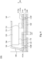
- Fig. 4 is a cross-sectional view of a package structure 100c according to some embodiments of the present disclosure.
- the difference between the package structure 100c in Figs. 4 and the package structure 100b in Fig. 3 is that the package structure 100c further includes a connection structure 180.
- the connection structure 180 has a first side 184 and a second side 186 opposite to the first side 184.
- the first side 184 faces the second side 156 of the chip 150 and the first conduction layer 110.
- the connection structure 180 is electrically connected to the second side 156 of the chip 150 and the first conduction layer 110.
- An area of an upper portion of the connection structure 180 that overlapped with the chip 150 along the first direction D1 is greater than an area of the second side 156 of the chip 150.
- an area of the upper portion of the connection structure 180 is five times to ten times greater than the area of the second side 156 of the chip 150.
- one connection structure 180 can collectively cover at least five chips 150 to increase the heat conduction area.
- the chip 150 can be grounded through the connection structure 180 by electrically connecting to the first conduction layer 110. Therefore, the thermal dissipation ability of the package structure 100c can be increased.
- the second portions 112B of the first conduction layer 110 can be replaced by the conductive via 140 as described about the package structure 100 illustrated in Fig. 1 .
- the second side 186 or the entire second side 186 of the connection structure 180 is free from coverage of the encapsulation 160.
- the second side 186 of the connection structure 180 can also be surrounded by the encapsulation 160.
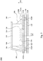
- Fig. 5 is a cross-sectional view of a package structure 100d according to some embodiments of the present disclosure.
- the package structure 100d further includes an isolation material 190.
- the isolation material 190 is disposed between the chip 150 and the first conduction layer 110 and wraps the bumps of the attach material 170. In other words, the isolation material 190 isolates the attach material 170 from the encapsulation 160.
- the isolation material 190 is composed of similar materials as the encapsulation 160 but with higher permeability and higher resistance to voltage.
- the isolation material 190 may further protect the attach material 170. Moreover, although the attach material 170 is fragile, the isolation material 190 with high permeability can be easily formed to wrap each bumps of the attach material 170 after the chip 150 has been connected with the first conduction layer 110. Therefore, the insulating ability and the stability of the package structure 100d can be increased. In the present embodiments, the isolation material 190 further covers the top surfaces 1122B of the second portions 112B of the first conduction layer 110. In some other embodiments, the isolation material 190 can be applied to package structures of the aforementioned embodiments illustrated in Figs. 1-4 .
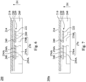
- Fig. 6 is a cross-sectional view of a package structure 200 according to some embodiments of the present disclosure.
- the package structure 200 includes a first conduction layer 210, a second conduction layer 220, and an isolation layer 230.
- the first conduction layer 210 includes at least one portion. In the present embodiment, the first conduction layer 210 is composed of a single portion.
- the second conduction layer 220 includes a plurality of portions 222.
- the isolation layer 230 is disposed between the first conduction layer 210 and the second conduction layer 220, and the isolation layer 230 is partially exposed from the second conduction layer 120.
- the isolation layer 230 is composed of one of nitride and oxide mixed with at least one of epoxy and polymer.
- the package structure 200 further includes a first chip 250A, a lead frame 270, and an encapsulation 260.
- the first chip 250A has a first side 254A and a second side 256A opposite to the first side 254A.
- the lead frame 270 includes a first portion 270A and a second portion 270B.
- the first portion 270A and the second portion 270B are electrically insulated from each other after the package structure 200 is encapsulated.
- the first portion 270A and the second portion 270B must be connected through bar structures before the package structure 200 is encapsulated.
- the second side 256A of the first chip 250A is electrically connected to the first portion 270A of the lead frame 270, and the first side 254A of the first chip 250A is electrically connected to the second conduction layer 220.
- the first chip 250A is attached on the lead frame 270 and the second conduction layer 220 with attach material (not shown) as described above about the package structure 100 illustrated in Fig. 1 .
- the encapsulation 260 covers the first chip 250A, the first conduction layer 210, the second conduction layer 220, the isolation layer 230, and the lead frame 270. In the present embodiment, a side of the lead frame 270 that is away from the first chip 250A is free from coverage of the encapsulation 260.
- the package structure 200 further includes two conductive vias 240 and a connection structure 280.
- the conductive vias 240 are electrically connected with the first conduction layer 210 and the second conduction layer 220.
- the connection structure 280 is disposed between the second conduction layer 220 and the second portion 270B of the lead frame 270.
- the second conduction layer 220 is electrically connected with the lead frame 270 through the connection structure 280.
- the configuration of the first conduction layer 210, the second conduction layer 220, the isolation layer 230, and the conductive vias 240 are similar to the configuration of the first conduction layer 110, the second conduction layer 120, the isolation layer 130, and the conductive vias 140 of the package structure 100 as described above about the package structure 100 illustrated in Fig. 1 . Therefore, the breakdown voltage of the package structure 200 can be increased, and the thermal resistance of the package structure 200 can be reduced.
- the conductive vias 240 can be replaced by portions of the first conduction layer 210 or the second conduction layer 220 as described above about the package structure 100b illustrated in Fig. 3 .
- the first conduction layer 210 has a side 214 that is away from the isolation layer 230. At least one portion of the side 214 or the entire side 214 of the first conduction layer 210 is free from coverage of the encapsulation 260. Therefore, the thermal dissipation ability of the package structure 200 can be increased. In some other embodiments, the side 214 of the first conduction layer 210 may be surrounded by the encapsulation 260.
- Fig. 7 is a cross-sectional view of a package structure 200a according to some embodiments of the present disclosure.
- the difference between the package structure 200a in Fig. 7 and the package structure 200 in Fig. 6 is that the second portion 270B of the lead frame 270 extends to the second conduction layer 220, and there is no connection structure 280. In other words, the second portion 270B is directly connected with the second conduction layer 220.
- Fig. 8 is a cross-sectional view of a package structure 200b according to some embodiments of the present disclosure.
- the package structure 200b further includes another first chips 250B.
- the first chip 250B is free from contacting the lead frame 270.
- a projection of the first chip 250B along the first direction D1 is not overlapped with the lead frame 270.
- the second side 256B of the first chip 250B is in contact with the encapsulation 260, while the second side 256A of the first chip 250A is not in contact with the encapsulation 260.
- the first chip 250A and the first chip 250B are attached on the second conduction layer 220 before being attached on the lead frame 270. Therefore, there is no need for supporting the first chip 250A and the first chip 250B by the lead frame 270. Moreover, the number of the pads of the lead frame 270 is limited due to the fabrication process, while the number of the pads of the second conduction layer 220 can be greater as described in the embodiments illustrated in Figs. 1-5 . Therefore, the number of the chips encapsulated in the package structure 200b can be increased. The forming method of the package structure 200b will be described in the following paragraphs accompanying Fig.11 and Figs. 12A-12D .
- Fig. 9 is a cross-sectional view of a package structure 200c according to some embodiments of the present disclosure.
- the package structure 200c further includes a second chip 350A, a pillar 290, and the lead frame 270 further includes a third portion 270C.
- the second chip 350A includes a side 354A facing the first conduction layer 210, and the second chip 350A is electrically connected to the first conduction layer 210.
- the pillar 290 is disposed between the second chip 350A and the third portion 270C of the lead frame 270.
- the pillar 290 is connected with the second chip 350A and the third portion 270C of the lead frame 270 through attach materials 292.
- the second chip 350A is electrically connected to the third portion 270C of the lead frame 270 through the pillar 290.
- the side 354A of the second chip 350A faces the pillar 290 and the third portion 270C of the lead frame 270.
- the encapsulation 260 covers the first chips 250A, 250B, the second chip 350A, the first conduction layer 210, the isolation layer 230, the second conduction layer 220, the lead frame 270, and the pillar 290. With such configuration, the number of chips encapsulated in the package structure 200c can be increased.
- the forming method of the package structure 200c will be described in the following paragraphs accompanying Fig.13 , and Figs. 14A-14F .
- Fig. 10 is a cross-sectional view of a package structure 200d according to some embodiments of the present disclosure.
- the difference between the package structure 200d in Fig. 10 and the package structure 200c in Fig. 9 is that the first conduction layer 210 includes a plurality of portions 212 and the package structure 200d further includes another second chips 350B.
- the second chip 350B is electrically connected to the portions 212 of the first conduction layer 210.
- the configuration between the second chip 350B and the first conduction layer 210 is similar to the configuration between the chip 150 and the first conduction layer 110 as described above about the package structure 100 illustrated in Fig.
- the configuration of the first conduction layer 210, the second conduction layer 220, the isolation layer 230, and the conductive vias 240 are the same as the configuration of the first conduction layer 110, the second conduction layer 120, the isolation layer 130, and the conductive via 140 of the package structure 100 as described above about the package structure 100 illustrated in Fig. 1 .
- the second chip 350B is electrically connected to the second conduction layer 220 sequentially through the first conduction layer 210 and the conductive vias 240. Therefore, the chips can be attached on both first conduction layer 210 and the second conduction layer 220, and the chips can be electrically connected to the lead frame 270 through connection structures 280 or pillar 290. Therefore, the number of chips that can be encapsulated in the package structure 200d can be further increased.
- Fig. 11 is a flow chart of a forming method of a package structure according to some embodiments of the present disclosure.
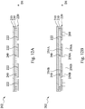
- Figs. 12A-12D are cross-sectional views of the package structure 200b illustrated in Fig. 8 at different intermediate stages of the forming method in Fig. 11 .
- the method starts with step S11, where a substrate 202 is formed.
- the substrate 202 includes a first conduction layer 210, a second conduction layer 220, and an isolation layer 230 disposed between the first conduction layer 210 and the second conduction layer 220.
- the first conduction layer 210 is composed of a single portion.
- the second conduction layer 220 includes a plurality of portions 222 electrically insulated and spaced apart from each other.
- the substrate 202 further includes conductive vias 240 disposed between and in contact with the first conduction layer 210 and the second conduction layer 220.
- a first chip 250A is attached on the second conduction layer 220.
- the first chip 250A includes a first side 254A and a second side 256A opposite to the first side 254A.
- the first side 254A is attached to the second conduction layer 220.
- another first chip 250B is attached on the second conduction layer 220, and two connection structures 280 are respectively attached to other two portions 222 of the second conduction layer 220.
- step S13 where first chips 250A are attached on the lead frame 270.
- the connection structures 280 and the first chips 250A are attached on the lead frame 270 simultaneously.
- the second side 256A of the first chip 250A is attached on the lead frame 270, while the first chip 250B is free from contacting the lead frame 270.
- step S14 where the encapsulation 260 is formed.
- the encapsulation 260 covers the substrate 202, the first chip 250A, 250B, and the lead frame 270.
- the second side 256B of the first chip 250B is in contact with the encapsulation 260, while the second side 256A of the first chip 250A is not in contact with the encapsulation 260.
- the number of the pads of the lead frame 270 is limited due to the fabrication process, while the number of the pads for positioning the chips formed by the second conduction layer 220 can be greater. Therefore, the number of the pads for positioning the chips formed by the second conduction layer 220 can be greater than the number of the pads on the lead frame 270. Therefore, the number of the chips that can be encapsulated in the package structure 200b can be increased.
- Fig. 13 is a flow chart of a forming method of a package structure according to some embodiments of the present disclosure.
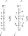
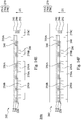
- Figs. 14A-14F are cross-sectional views of the package structure 200c illustrated in Fig. 9 at different intermediate stages of the forming method in Fig. 13 .
- Reference is made to Figs. 13 and 14A the method starts with step S21, where a substrate 202 is formed.
- the forming method about the substrate 202 is the same as the forming method described in Fig. 11 and Fig. 12A . Therefore, a description in this regard will not be repeated hereinafter.
- step S22 where a first chip 250A is attached on the second conduction layer 220.
- Other structural details of step S22 are similar to those described in step S12. Therefore, a description in this regard will not be repeated hereinafter.
- step S23 where a pillar 290 is attached on the lead frame 270.
- the pillar 290 is attached on the third portion 270C by the attach material 292.
- step S24 where the first chips 250A is attached on the lead frame 270.
- the connection structures 280 and the first chips 250A are attached on the lead frame 270 simultaneously.
- Other structural details between the first chips 250A, 250B, and the lead frame 270 are similar to those described in step S13. Therefore, a description in this regard will not be repeated hereinafter for simplicity.
- step S25 a second chip 350A is attached on the first conduction layer 210 and the pillar 290.
- the second chip 350A is attached on the pillar 290 by the attach material 292. Therefore, the second chip 350A is electrically connected with the first conductor layer 210 and the lead frame 270.
- step S26 where the encapsulation 260 is formed.
- the encapsulation 260 covers the substrate 202, the first chip 250A, the first chip 250B, the second chip 350A, the lead frame 270, and the pillar 290.
- the configuration of the package structure 200d in Fig. 10 can be formed by modifying the steps S21 and S22.
- the step S21 can be modified to further include forming a plurality of portions 212 of the first conduction layer 210 and forming conductive vias 240 in the isolation layer 230.
- the step S22 can be modified to further include attaching a second chip 350B on the portions 212 of the first conduction layer 210.
- the chips can be attached on both first conduction layer 210 and the second conduction layer 220, and the chips can be electrically connected to lead frame through connection structures 280 or pillar 290. Therefore, the number of chips that can be encapsulated in the package structure 200d can be further increased.
Landscapes
- Structures Or Materials For Encapsulating Or Coating Semiconductor Devices Or Solid State Devices (AREA)
- Engineering & Computer Science (AREA)
- Microelectronics & Electronic Packaging (AREA)
Abstract
A package structure includes a first conduction layer, a second conduction layer, and an isolation layer. The first conduction layer includes a plurality of first portions, and the second conduction layer includes a plurality of portions. The isolation layer is disposed between the first conduction layer and the second conduction layer, and the isolation layer is composed of one of nitride and oxide mixed with at least one of epoxy and polymer.
Description
- The present invention relates to a package structure and a forming method of a package structure.
- Improvements in power semiconductor device have introduced some issues. For example, when the applied voltage is higher, the thermal resistance becomes higher and the insulating ability may not be enough to withstand high voltage. Therefore, there is a need for a package structure with higher breakdown voltage and lower thermal resistance.
- Furthermore, a typical lead frame may be deformed due to the weight of the chips. Therefore, the die attachment process may be unstable and the yield rate is limited. Thus, there is also a need for a package structure that makes the die attachment process be more stable.
- An aspect of the present disclosure is to provide a package structure.
- In some embodiments, the package structure includes a first conduction layer, a second conduction layer, and an isolation layer. The first conduction layer includes a plurality of first portions, and the second conduction layer includes a plurality of portions. The isolation layer is disposed between the first conduction layer and the second conduction layer, and the isolation layer is composed of one of nitride and oxide mixed with at least one of epoxy and polymer.
- In some embodiments, the package structure further includes a conductive via disposed between and in contact with the first conduction layer and the second conduction layer.
- In some embodiments, the first conduction layer further includes a second portion connecting with adjacent two of the first portions of the first conduction layer. The second portion of the first conduction layer has a top surface, and a portion of a top surface of the second portion is free from coverage of the two first portions.
- In some embodiments, the package structure further includes a chip and an encapsulation. The chip is electrically connected to the first conduction layer. The chip includes a first side and a second side opposite to the first side, and the first side faces the first conduction layer. The encapsulation covers the chip and the first conduction layer.
- In some embodiments, a portion of the second side of the chip is free from coverage of the encapsulation.
- In some embodiments, the package structure further includes a connection structure having a first side electrically connected to the second side of the chip and the first conduction layer.
- In some embodiments, the connection structure further includes a second side opposite to the first side thereof, and a portion of the second side of the connection structure is free from coverage of the encapsulation.
- In some embodiments, the package structure further includes an attach material disposed between the first side of the chip and the first portions of the first conduction layer.
- In some embodiments, the package structure further includes an isolation material isolating the attach material from the encapsulation.
- Another aspect of the present disclosure is to provide a package structure.
- The package structure includes a first conduction layer, a second conduction layer, and an isolation layer. The first conduction layer includes at least one portion, and the second conduction layer includes a plurality of portions. The isolation layer is disposed between the first conduction layer and the second conduction layer, and the isolation layer is composed of one of nitride and oxide mixed with at least one of epoxy and polymer.
- In some embodiments, the package structure further includes at least one chip and a lead frame. The chip includes a first side and a second side opposite to the first side, and the second side is electrically connected to the second conduction layer. The lead frame includes a first portion electrically connected to the first side of the chip.
- In some embodiments, the package structure further includes an encapsulation covering the chip, the first conduction layer, the second conduction layer, and the lead frame.
- In some embodiments, a portion of a side of the first conduction layer away from the isolation layer is free from coverage of the encapsulation.
- In some embodiments, the lead frame further includes a second portion. The package structure further includes a connection structure disposed between the second conduction layer and the second portion of the lead frame.
- In some embodiments, the lead frame further includes a second portion extending to the second conduction layer.
- In some embodiments, the package structure further includes a lead frame and a plurality of chips. The lead frame includes a plurality of portions. The chips are disposed between the second conduction layer and the lead frame, and one of the chips is free from contacting the lead frame.
- In some embodiments, the package structure further includes a chip including a side that faces the first conduction layer, and the chip is electrically connected to the first conduction layer.
- In some embodiments, the package structure further includes a lead frame and a pillar. The first conduction layer is disposed between the lead frame and the chip, and the pillar is disposed between the chip and the lead frame.
- In some embodiments, the package structure further includes an encapsulation covering the chip, the first conduction layer, the isolation layer, the second conduction layer, and the lead frame.
- In some embodiments, a number of the at least one portion of the first conduction layer is plural, and the package structure further includes a plurality of chips electrically connected to the portions of the first conduction layer.
- Another aspect of the present disclosure is to provide a forming method of a package structure.
- The forming method of a package structure includes forming a substrate including a first conduction layer, a second conduction layer, and an isolation layer disposed between the first conduction layer and the second conduction layer; attaching a first side of a first chip with the second conduction layer of the substrate; attaching a second side of the first chip opposite to the first side with a lead frame; and encapsulating the substrate, the chip, and the lead frame.
- In some embodiments, the forming method of a package structure further includes attaching a connection structure with the second conduction layer of the substrate before attaching the second side of the first chip with the lead frame; and attaching the connection structure with the lead frame.
- In some embodiments, the forming method of a package structure further includes attaching a second chip with the first conduction layer and the pillar before encapsulating the substrate, the chip, and the lead frame.
- In some embodiments, the forming method of a package structure further includes attaching a pillar with the lead frame before attaching the second side of the chip with the lead frame.
- In the aforementioned embodiments, the isolation layer can increase the insulating ability and provide a supporting force that prevents the first conduction layer and the second conduction layer from bending during the die attachment process. Therefore, the breakdown voltage of the package structure can be increased, and the yield rate of the package structure can be improved. Furthermore, an overlapping region can exist between the first conduction layer and the second conduction layer. Therefore, the thermal dissipation ability can be increased, and the thermal resistance can be reduced.
- It is to be understood that both the foregoing general description and the following detailed description are by examples, and are intended to provide further explanation of the invention as claimed.
- The invention can be more fully understood by reading the following detailed description of the embodiment, with reference made to the accompanying drawings as follows:
-
Figs. 1-5 are cross-sectional views of package structures according to some embodiments of the present disclosure. -
Figs. 6-10 are cross-sectional views of package structures according to some other embodiments of the present disclosure. -
Fig. 11 is a flow chart of the forming method of a package structure according to one embodiment of the present disclosure. -
Figs. 12A-12D are cross-sectional views of the package structure inFig. 8 at different intermediate stages of the forming method inFig. 11 . -
Fig. 13 is a flow chart of the forming method of a package structure according to one embodiment of this invention. -
Figs. 14A-14F are cross-sectional views of the package structure inFig. 9 at different intermediate stages of the forming method inFig. 13 . - Reference will now be made in detail to the present embodiments of the invention, examples of which are illustrated in the accompanying drawings. Wherever possible, the same reference numbers are used in the drawings and the description to refer to the same or like parts.
-
Fig. 1 is a cross-sectional view of apackage structure 100 according to some embodiments of the present disclosure. Thepackage structure 100 includes afirst conduction layer 110, asecond conduction layer 120, and anisolation layer 130. Thefirst conduction layer 110 has a plurality offirst portions 112A. Thesecond conduction layer 120 has a plurality ofportions 122. Thefirst portions 112A of thefirst conduction layer 110 are electrically insulated and spaced apart from each other, and theportions 122 of thesecond conduction layer 120 are electrically insulated and spaced apart from each other. Theisolation layer 130 is disposed between thefirst conduction layer 110 and thesecond conduction layer 120, and theisolation layer 130 is partially exposed from thefirst conduction layer 110 and thesecond conduction layer 120. Theisolation layer 130 is composed of one of nitride and oxide mixed with at least one of epoxy and polymer. Therefore, the thickness of theisolation layer 130 can be minimized. For example, in some embodiments, the thickness of theisolation layer 130 is less than 150 micrometers and greater than 40 micrometers. In some other embodiments, the thickness of theisolation layer 130 is less than 150 micrometers and greater than 10 micrometers, but the present disclosure is not limited in this regard. - The
package structure 100 further includes twoconductive vias 140, achip 150, anencapsulation 160, and an attachmaterial 170. Theconductive vias 140 are disposed between and in contact with thefirst conduction layer 110 and thesecond conduction layer 120. Thefirst conduction layer 110 is electrically connected with thesecond conduction layer 120 through theconductive vias 140. Specifically, as illustrated inFig. 1 , twofirst portions 112A are electrically connected with twoportions 122 of thesecond conduction layer 120 through twoconduction vias 140, respectively. However, one of thefirst portions 112A of the first conduction layer 110 (e.g., thefirst portion 112A on the left-hand side) is electrically insulated from one of theportions 122 of the second conduction layer 120 (e.g., theportion 122 on the right-hand side) by theisolation layer 130. Thechip 150 includes afirst side 154 and asecond side 156 opposite to thefirst side 154. Thefirst side 154 faces thefirst conduction layer 110, and thesecond side 156 faces away from thefirst conduction layer 110. The attachmaterial 170 includes a plurality of bumps each disposed between thefirst side 154 of the chip and thefirst conduction layer 110. Thechip 150 is electrically connected to at least twofirst portions 112A of thefirst conduction layer 110 through a plurality of bumps of the attachmaterial 170. Theencapsulation 160 covers thechip 150, the attachmaterial 170, and thefirst conduction layer 110. In the present embodiments, thesecond side 156 of thechip 150 is entirely covered by theencapsulation 160, and theencapsulation 160 surrounds thechip 150 and the attachmaterial 170. As shown inFig. 1 , a portion of theisolation layer 130 that is exposed from thefirst conduction layer 110 is in contact with theencapsulation 160. In some embodiments, theencapsulation 160 is composed of, for example, epoxy or polymer. - A typical lead frame includes a pattern designed based on the signal transmission path between a chip (such as the chip 150) and an external device, for example, a printed circuit board. The pattern of the lead frame is at least composed of die pads, inner leads, outer leads, and bar structures that connect those leads to support the pattern of the lead frame before the chip is encapsu lated.
- In the present embodiment, the
first portions 112A of thefirst conduction layer 110 form a pattern, theportions 122 of thesecond conduction layer 120 form another pattern, and these two patterns are separated by theisolation layer 130. In other words, the pattern of thefirst conduction layer 110 and the pattern of thesecond conduction layer 120 connected throughconductive vias 140 can form signal transmission paths that replace the typical lead frame. - However, since the
isolation layer 130 is in contact with the entire pattern of thefirst conduction layer 110,first portions 112A of thefirst conduction layer 110 can be isolated from each other without connected by bar structures used in conventional package structures. Similarly, since theisolation layer 130 is in contact with the entire pattern of thesecond conduction layer 120,portions 122 of thesecond conduction layer 120 can be isolated from each other without connected by the bar structures. In other words, since theisolation layer 130 is disposed between thefirst conduction layer 110 and thesecond conduction layer 120, the patterns of thefirst conduction layer 110 and thesecond conduction layer 120 can be supported by theisolation layer 130. Therefore, the design flexibility of the patterns of thefirst conduction layer 110 and thesecond conduction layer 120 can be increased. Accordingly, the densities of the die pads and the leads (e.g.,first portions 112A and portions 122) of thefirst conduction layer 110 and thesecond conduction layer 120 can be increased. - During a typical die attachment process, the lead frame is deformed due to the weight of the chip. Therefore, the yield rate of the package structure is limited. The
isolation layer 130 of the present disclosure can provide a supporting force that prevents thefirst conduction layer 110 and thesecond conduction layer 120 from bending during the die attachment process. Accordingly, the die attachment process can be more stable and the yield rate of thepackage structure 100 can be improved. - A high power semiconductor device requires a higher insulating ability for applications with high voltage. Otherwise, when the insulating ability provided by the
encapsulation 160 is not enough, device failure may happen. Theisolation layer 130 of the present disclosure can increase the insulating ability, thereby increasing the breakdown voltage of thepackage structure 100. In some embodiments, the breakdown voltage can be increased by four times. In some embodiments, thechip 150 is a high power semiconductor device, and is composed of gallium nitride (GaN) or silicon carbide (SiC). In some other embodiments, thechip 150 is a silicon-based semiconductor device. - As shown in
Fig. 1 , along a first direction D1 extending from thesecond conduction layer 120 to thefirst conduction layer 110, one of thefirst portions 112A (on the left-hand side) of thefirst conduction layer 110 and one of the portions 122 (on the right-hand side) of thesecond conduction layer 120 that are electrically insulated from each other are partially overlapped (as indicated by the overlapping region OV). In other words, a projection of thefirst portion 112A (on the left-hand side) along the first direction D1 and a projection of the portion 122 (on the right-hand side) along the first direction D1 are overlapped. Therefore, the area for heat conduction can be increased. Accordingly, the thermal dissipation ability can be increased, and the thermal resistance can be reduced. -
Fig. 2 is a cross-sectional view of apackage structure 100a according to some embodiments of the present disclosure. The difference between thepackage structure 100a inFigs. 2 and thepackage structure 100 inFig. 1 is that at least a portion of thesecond side 156 of thechip 150 is free from coverage of theencapsulation 160. In the present embodiment, as shown inFig. 2 , the entiresecond side 156 of thechip 150 is exposed from theencapsulation 160. In some other embodiments, at least a portion of thesecond side 156 is exposed from theencapsulation 160. In other words, thesecond side 156 of thechip 150 is partially covered by theencapsulation 160. - In some embodiments, in order to expose the
second side 156 of thechip 150, thesecond side 156 of thechip 150 may be covered by a tape before encapsulating thechip 150, and the tape may be removed after theencapsulation 160 is formed. In some other embodiments, an upper part of the encapsulation above thechip 150 is polished to expose thesecond side 156 of thechip 150. Therefore, the thermal dissipation ability of thepackage structure 100a can be further increased. -
Fig. 3 is a cross-sectional view of apackage structure 100b according to some embodiments of the present disclosure. The difference between thepackage structure 100b inFigs. 3 and thepackage structure 100a inFig. 2 is the configurations of thefirst conduction layer 110. Thefirst conduction layer 110 of thepackage structure 100b includes a plurality ofsecond portions 112B and there is no conductive via 140. Each of thesecond portions 112B of thefirst conduction layer 110 is connected with adjacent two of thefirst portions 112A of thefirst conduction layer 110. Each of thesecond portions 112B of thefirst conduction layer 110 has atop surface 1122B, and a portion of thetop surface 1122B of each of thesecond portions 112B is free from coverage of the adjacent twofirst portions 112A. In other words, thesecond portions 112B extend from thefirst portions 112A toward thesecond conduction layer 120 and thesecond portions 112B are surrounded by theisolation layer 130. Therefore, the electrical connection between thefirst conduction layer 110 and thesecond conduction layer 120 can be formed simultaneously within the same process step of forming thefirst conduction layer 110. As a result, the fabrication process can be simplified. -
Fig. 4 is a cross-sectional view of apackage structure 100c according to some embodiments of the present disclosure. The difference between thepackage structure 100c inFigs. 4 and thepackage structure 100b inFig. 3 is that thepackage structure 100c further includes aconnection structure 180. Theconnection structure 180 has afirst side 184 and asecond side 186 opposite to thefirst side 184. Thefirst side 184 faces thesecond side 156 of thechip 150 and thefirst conduction layer 110. Theconnection structure 180 is electrically connected to thesecond side 156 of thechip 150 and thefirst conduction layer 110. - An area of an upper portion of the
connection structure 180 that overlapped with thechip 150 along the first direction D1 is greater than an area of thesecond side 156 of thechip 150. In some embodiments, an area of the upper portion of theconnection structure 180 is five times to ten times greater than the area of thesecond side 156 of thechip 150. As such, oneconnection structure 180 can collectively cover at least fivechips 150 to increase the heat conduction area. Furthermore, thechip 150 can be grounded through theconnection structure 180 by electrically connecting to thefirst conduction layer 110. Therefore, the thermal dissipation ability of thepackage structure 100c can be increased. In the present embodiments, thesecond portions 112B of thefirst conduction layer 110 can be replaced by the conductive via 140 as described about thepackage structure 100 illustrated inFig. 1 . - In the present embodiment, at least a portion of the
second side 186 or the entiresecond side 186 of theconnection structure 180 is free from coverage of theencapsulation 160. In some other embodiments, thesecond side 186 of theconnection structure 180 can also be surrounded by theencapsulation 160. -
Fig. 5 is a cross-sectional view of apackage structure 100d according to some embodiments of the present disclosure. The difference between thepackage structure 100d inFigs. 5 and thepackage structure 100c inFig. 4 is that thepackage structure 100d further includes anisolation material 190. Theisolation material 190 is disposed between thechip 150 and thefirst conduction layer 110 and wraps the bumps of the attachmaterial 170. In other words, theisolation material 190 isolates the attach material 170 from theencapsulation 160. In some embodiments, theisolation material 190 is composed of similar materials as theencapsulation 160 but with higher permeability and higher resistance to voltage. Since the attachmaterial 170 is critical to the electrical connection performance of thepackage structure 100d, theisolation material 190 may further protect the attachmaterial 170. Moreover, although the attachmaterial 170 is fragile, theisolation material 190 with high permeability can be easily formed to wrap each bumps of the attachmaterial 170 after thechip 150 has been connected with thefirst conduction layer 110. Therefore, the insulating ability and the stability of thepackage structure 100d can be increased. In the present embodiments, theisolation material 190 further covers thetop surfaces 1122B of thesecond portions 112B of thefirst conduction layer 110. In some other embodiments, theisolation material 190 can be applied to package structures of the aforementioned embodiments illustrated inFigs. 1-4 . -
Fig. 6 is a cross-sectional view of apackage structure 200 according to some embodiments of the present disclosure. Thepackage structure 200 includes afirst conduction layer 210, asecond conduction layer 220, and anisolation layer 230. Thefirst conduction layer 210 includes at least one portion. In the present embodiment, thefirst conduction layer 210 is composed of a single portion. Thesecond conduction layer 220 includes a plurality ofportions 222. Theisolation layer 230 is disposed between thefirst conduction layer 210 and thesecond conduction layer 220, and theisolation layer 230 is partially exposed from thesecond conduction layer 120. Theisolation layer 230 is composed of one of nitride and oxide mixed with at least one of epoxy and polymer. - The
package structure 200 further includes afirst chip 250A, alead frame 270, and anencapsulation 260. Thefirst chip 250A has afirst side 254A and asecond side 256A opposite to thefirst side 254A. Thelead frame 270 includes afirst portion 270A and asecond portion 270B. Thefirst portion 270A and thesecond portion 270B are electrically insulated from each other after thepackage structure 200 is encapsulated. However, as described above, thefirst portion 270A and thesecond portion 270B must be connected through bar structures before thepackage structure 200 is encapsulated. Thesecond side 256A of thefirst chip 250A is electrically connected to thefirst portion 270A of thelead frame 270, and thefirst side 254A of thefirst chip 250A is electrically connected to thesecond conduction layer 220. Thefirst chip 250A is attached on thelead frame 270 and thesecond conduction layer 220 with attach material (not shown) as described above about thepackage structure 100 illustrated inFig. 1 . Theencapsulation 260 covers thefirst chip 250A, thefirst conduction layer 210, thesecond conduction layer 220, theisolation layer 230, and thelead frame 270. In the present embodiment, a side of thelead frame 270 that is away from thefirst chip 250A is free from coverage of theencapsulation 260. - In the present embodiment, the
package structure 200 further includes twoconductive vias 240 and aconnection structure 280. Theconductive vias 240 are electrically connected with thefirst conduction layer 210 and thesecond conduction layer 220. Theconnection structure 280 is disposed between thesecond conduction layer 220 and thesecond portion 270B of thelead frame 270. Thesecond conduction layer 220 is electrically connected with thelead frame 270 through theconnection structure 280. - The configuration of the
first conduction layer 210, thesecond conduction layer 220, theisolation layer 230, and theconductive vias 240 are similar to the configuration of thefirst conduction layer 110, thesecond conduction layer 120, theisolation layer 130, and theconductive vias 140 of thepackage structure 100 as described above about thepackage structure 100 illustrated inFig. 1 . Therefore, the breakdown voltage of thepackage structure 200 can be increased, and the thermal resistance of thepackage structure 200 can be reduced. In some other embodiments, theconductive vias 240 can be replaced by portions of thefirst conduction layer 210 or thesecond conduction layer 220 as described above about thepackage structure 100b illustrated inFig. 3 . - In the present embodiment, the
first conduction layer 210 has aside 214 that is away from theisolation layer 230. At least one portion of theside 214 or theentire side 214 of thefirst conduction layer 210 is free from coverage of theencapsulation 260. Therefore, the thermal dissipation ability of thepackage structure 200 can be increased. In some other embodiments, theside 214 of thefirst conduction layer 210 may be surrounded by theencapsulation 260. -
Fig. 7 is a cross-sectional view of apackage structure 200a according to some embodiments of the present disclosure. The difference between thepackage structure 200a inFig. 7 and thepackage structure 200 inFig. 6 is that thesecond portion 270B of thelead frame 270 extends to thesecond conduction layer 220, and there is noconnection structure 280. In other words, thesecond portion 270B is directly connected with thesecond conduction layer 220. -
Fig. 8 is a cross-sectional view of apackage structure 200b according to some embodiments of the present disclosure. The difference between thepackage structure 200b inFig. 8 and thepackage structure 200a inFig. 7 is that thepackage structure 200b further includes anotherfirst chips 250B. As shown inFig. 8 , thefirst chip 250B is free from contacting thelead frame 270. In other words, a projection of thefirst chip 250B along the first direction D1 is not overlapped with thelead frame 270. Thesecond side 256B of thefirst chip 250B is in contact with theencapsulation 260, while thesecond side 256A of thefirst chip 250A is not in contact with theencapsulation 260. - In the present embodiment, the
first chip 250A and thefirst chip 250B are attached on thesecond conduction layer 220 before being attached on thelead frame 270. Therefore, there is no need for supporting thefirst chip 250A and thefirst chip 250B by thelead frame 270. Moreover, the number of the pads of thelead frame 270 is limited due to the fabrication process, while the number of the pads of thesecond conduction layer 220 can be greater as described in the embodiments illustrated inFigs. 1-5 . Therefore, the number of the chips encapsulated in thepackage structure 200b can be increased. The forming method of thepackage structure 200b will be described in the following paragraphs accompanyingFig.11 andFigs. 12A-12D . -
Fig. 9 is a cross-sectional view of apackage structure 200c according to some embodiments of the present disclosure. The difference between thepackage structure 200c inFig. 9 and thepackage structure 200b inFig. 8 is that thepackage structure 200c further includes asecond chip 350A, apillar 290, and thelead frame 270 further includes athird portion 270C. Thesecond chip 350A includes aside 354A facing thefirst conduction layer 210, and thesecond chip 350A is electrically connected to thefirst conduction layer 210. Thepillar 290 is disposed between thesecond chip 350A and thethird portion 270C of thelead frame 270. Thepillar 290 is connected with thesecond chip 350A and thethird portion 270C of thelead frame 270 through attachmaterials 292. Thesecond chip 350A is electrically connected to thethird portion 270C of thelead frame 270 through thepillar 290. In other words, theside 354A of thesecond chip 350A faces thepillar 290 and thethird portion 270C of thelead frame 270. Theencapsulation 260 covers thefirst chips second chip 350A, thefirst conduction layer 210, theisolation layer 230, thesecond conduction layer 220, thelead frame 270, and thepillar 290. With such configuration, the number of chips encapsulated in thepackage structure 200c can be increased. The forming method of thepackage structure 200c will be described in the following paragraphs accompanyingFig.13 , andFigs. 14A-14F . -
Fig. 10 is a cross-sectional view of apackage structure 200d according to some embodiments of the present disclosure. The difference between thepackage structure 200d inFig. 10 and thepackage structure 200c inFig. 9 is that thefirst conduction layer 210 includes a plurality ofportions 212 and thepackage structure 200d further includes anothersecond chips 350B. Thesecond chip 350B is electrically connected to theportions 212 of thefirst conduction layer 210. Specifically, the configuration between thesecond chip 350B and thefirst conduction layer 210 is similar to the configuration between thechip 150 and thefirst conduction layer 110 as described above about thepackage structure 100 illustrated inFig. 1 In other words, the configuration of thefirst conduction layer 210, thesecond conduction layer 220, theisolation layer 230, and theconductive vias 240 are the same as the configuration of thefirst conduction layer 110, thesecond conduction layer 120, theisolation layer 130, and the conductive via 140 of thepackage structure 100 as described above about thepackage structure 100 illustrated inFig. 1 . - The
second chip 350B is electrically connected to thesecond conduction layer 220 sequentially through thefirst conduction layer 210 and theconductive vias 240. Therefore, the chips can be attached on bothfirst conduction layer 210 and thesecond conduction layer 220, and the chips can be electrically connected to thelead frame 270 throughconnection structures 280 orpillar 290. Therefore, the number of chips that can be encapsulated in thepackage structure 200d can be further increased. -
Fig. 11 is a flow chart of a forming method of a package structure according to some embodiments of the present disclosure.Figs. 12A-12D are cross-sectional views of thepackage structure 200b illustrated inFig. 8 at different intermediate stages of the forming method inFig. 11 . Reference is made toFigs. 11 and12A , the method starts with step S11, where asubstrate 202 is formed. Thesubstrate 202 includes afirst conduction layer 210, asecond conduction layer 220, and anisolation layer 230 disposed between thefirst conduction layer 210 and thesecond conduction layer 220. Thefirst conduction layer 210 is composed of a single portion. Thesecond conduction layer 220 includes a plurality ofportions 222 electrically insulated and spaced apart from each other. Thesubstrate 202 further includesconductive vias 240 disposed between and in contact with thefirst conduction layer 210 and thesecond conduction layer 220. - Reference is made to
Figs. 11 and12B , the method continues with step S12, where afirst chip 250A is attached on thesecond conduction layer 220. Thefirst chip 250A includes afirst side 254A and asecond side 256A opposite to thefirst side 254A. Thefirst side 254A is attached to thesecond conduction layer 220. In the present embodiment, anotherfirst chip 250B is attached on thesecond conduction layer 220, and twoconnection structures 280 are respectively attached to other twoportions 222 of thesecond conduction layer 220. - Reference is made to
Figs. 11 and12C , the method continues with step S13, wherefirst chips 250A are attached on thelead frame 270. In the present embodiments, theconnection structures 280 and thefirst chips 250A, are attached on thelead frame 270 simultaneously. Specifically, as shown inFig. 12C , thesecond side 256A of thefirst chip 250A is attached on thelead frame 270, while thefirst chip 250B is free from contacting thelead frame 270. - Reference is made to
Figs. 11 and12D , the method continues with step S14, where theencapsulation 260 is formed. Theencapsulation 260 covers thesubstrate 202, thefirst chip lead frame 270. As shown inFigs. 12C and 12D , thesecond side 256B of thefirst chip 250B is in contact with theencapsulation 260, while thesecond side 256A of thefirst chip 250A is not in contact with theencapsulation 260. - As discussed above about the
package structure 200b illustrated inFig. 8 , the number of the pads of thelead frame 270 is limited due to the fabrication process, while the number of the pads for positioning the chips formed by thesecond conduction layer 220 can be greater. Therefore, the number of the pads for positioning the chips formed by thesecond conduction layer 220 can be greater than the number of the pads on thelead frame 270. Therefore, the number of the chips that can be encapsulated in thepackage structure 200b can be increased. -
Fig. 13 is a flow chart of a forming method of a package structure according to some embodiments of the present disclosure.Figs. 14A-14F are cross-sectional views of thepackage structure 200c illustrated inFig. 9 at different intermediate stages of the forming method inFig. 13 . Reference is made toFigs. 13 and14A , the method starts with step S21, where asubstrate 202 is formed. The forming method about thesubstrate 202 is the same as the forming method described inFig. 11 andFig. 12A . Therefore, a description in this regard will not be repeated hereinafter. - Reference is made to
Figs. 13 and14B , the method continues with step S22, where afirst chip 250A is attached on thesecond conduction layer 220. Other structural details of step S22 are similar to those described in step S12. Therefore, a description in this regard will not be repeated hereinafter. - Reference is made to
Figs. 13 and14C , the method continues with step S23, where apillar 290 is attached on thelead frame 270. Thepillar 290 is attached on thethird portion 270C by the attachmaterial 292. - Reference is made to
Figs. 13 and14D , the method continues with step S24, where thefirst chips 250A is attached on thelead frame 270. In the present embodiments, theconnection structures 280 and thefirst chips 250A are attached on thelead frame 270 simultaneously. Other structural details between thefirst chips lead frame 270 are similar to those described in step S13. Therefore, a description in this regard will not be repeated hereinafter for simplicity. - Reference is made to
Figs. 13 and14E , the method continues with step S25, where asecond chip 350A is attached on thefirst conduction layer 210 and thepillar 290. Thesecond chip 350A is attached on thepillar 290 by the attachmaterial 292. Therefore, thesecond chip 350A is electrically connected with thefirst conductor layer 210 and thelead frame 270. - Reference is made to
Figs. 13 and14F , the method continues with step S26, where theencapsulation 260 is formed. Theencapsulation 260 covers thesubstrate 202, thefirst chip 250A, thefirst chip 250B, thesecond chip 350A, thelead frame 270, and thepillar 290. - It is noted that the configuration of the
package structure 200d inFig. 10 can be formed by modifying the steps S21 and S22. For example, the step S21 can be modified to further include forming a plurality ofportions 212 of thefirst conduction layer 210 and formingconductive vias 240 in theisolation layer 230. The step S22 can be modified to further include attaching asecond chip 350B on theportions 212 of thefirst conduction layer 210. - As discussed above, with such configuration, the chips can be attached on both
first conduction layer 210 and thesecond conduction layer 220, and the chips can be electrically connected to lead frame throughconnection structures 280 orpillar 290. Therefore, the number of chips that can be encapsulated in thepackage structure 200d can be further increased.
Claims (15)
- A package structure (100), characterized by comprising:a first conduction layer (110) comprising a plurality of first portions (112A);a second conduction layer (120) comprising a plurality of portions (122), andan isolation layer (130) disposed between the first conduction layer (110) and the second conduction layer (120), wherein the isolation layer (130) is composed of one of nitride and oxide mixed with at least one of epoxy and polymer.
- The package structure (100) of claim 1, further comprising:
a conductive via (140) disposed between and in contact with the first conduction layer (110) and the second conduction layer (120). - The package structure (100) of one of the claims 1 to 2, wherein the first conduction layer (110) further comprises:
a second portion (112B) connecting with adjacent two of the first portions (112A) of the first conduction layer (110), wherein the second portion (112B) of the first conduction layer (110) has a top surface, and a portion of a top surface (1122B) of the second portion (112B) is free from coverage of the two first portions (112A). - The package structure (100) of one of the claims 1 to 3, further comprising:a chip (150) electrically connected to the first conduction layer (110), wherein the chip (150) comprises a first side (154) and a second side (156) opposite to the first side (154), and the first side (154) faces the first conduction layer (110); andan encapsulation(160) covering the chip (150) and the first conduction layer (110).
- The package structure (100) of claim 4, wherein a portion of the second side (156) of the chip (150) is free from coverage of the encapsulation (160).
- The package structure (100) of one of the claims 4 to 5, further comprising:
a connection structure (180) having a first side (184) electrically connected to the second side (156) of the chip (150) and the first conduction layer (110). - The package structure (100) of claim 6, wherein the connection structure (180) further comprises a second side (186) opposite to the first side (184) thereof, and a portion of the second side (186) of the connection structure (180) is free from coverage of the encapsulation (160).
- The package structure (100) of one of the claims 4 to 7, further comprising:
an attach material (170) disposed between the first side (154) of the chip (150) and the first portions (112A) of the first conduction layer (110). - The package structure (100) of claim 8, further comprising:
an isolation material (190) isolating the attach material (170) from the encapsulation (160). - A method of forming a package structure (200), characterized by comprising:forming a substrate (202) comprising a first conduction layer (210), a second conduction layer (220), and an isolation layer (230) disposed between the first conduction layer (210) and the second conduction layer (220);attaching a first side (254A) of a first chip (250A) with the second conduction layer (220) of the substrate (202);attaching a second side (256A) of the first chip (250A) opposite to the first side (254A) with a lead frame (270); andencapsulating the substrate (202), the first chip (250A), and the lead frame (270).
- The method of claim 10, wherein forming the substrate (202) comprises:
forming a conductive via (240) between the first conduction layer (210) and the second conduction layer (220). - The method of one of the claims 10 to 11, wherein forming the substrate (202) comprises:
forming the first conduction layer (110) comprising a plurality of first portions (112A) and a second portion (112B) connecting with adjacent two of the first portions (112A). - The method of one of the claims 10 to 12, further comprising:attaching a connection structure (280) with the second conduction layer (220) of the substrate (202) before attaching the second side (256A) of the first chip (250A) with the lead frame (270); andattaching the connection structure (280) with the lead frame (270).
- The method of one of the claims 10 to 13, further comprising:
attaching a pillar (290) with the lead frame (270) before attaching the second side (256A) of the chip (250A) with the lead frame (270). - The method of claim 14, further comprising:
attaching a second chip (250B) with the first conduction layer (210) and the pillar (290) before encapsulating the substrate (202), the chip (250A), and the lead frame (270).
Applications Claiming Priority (2)
| Application Number | Priority Date | Filing Date | Title |
|---|---|---|---|
| US201962798487P | 2019-01-30 | 2019-01-30 | |
| US16/551,717 US20200243430A1 (en) | 2019-01-30 | 2019-08-27 | Package structure and forming method of the same |
Publications (1)
| Publication Number | Publication Date |
|---|---|
| EP3712934A1 true EP3712934A1 (en) | 2020-09-23 |
Family
ID=71732821
Family Applications (1)
| Application Number | Title | Priority Date | Filing Date |
|---|---|---|---|
| EP19218103.0A Withdrawn EP3712934A1 (en) | 2019-01-30 | 2019-12-19 | Package structure and forming method of the same |
Country Status (4)
| Country | Link |
|---|---|
| US (1) | US20200243430A1 (en) |
| EP (1) | EP3712934A1 (en) |
| CN (1) | CN111508907A (en) |
| TW (1) | TWI713164B (en) |
Families Citing this family (1)
| Publication number | Priority date | Publication date | Assignee | Title |
|---|---|---|---|---|
| JP2023036447A (en) * | 2021-09-02 | 2023-03-14 | 新電元工業株式会社 | Lead frame integrated substrate, semiconductor device, manufacturing method of lead frame integrated substrate, and manufacturing method of semiconductor device |
Citations (11)
| Publication number | Priority date | Publication date | Assignee | Title |
|---|---|---|---|---|
| WO2001024260A1 (en) * | 1999-09-24 | 2001-04-05 | Virginia Tech Intellectual Properties, Inc. | Low cost 3d flip-chip packaging technology for integrated power electronics modules |
| US20020187318A1 (en) * | 2000-12-27 | 2002-12-12 | Yoshihisa Yamashita | Lead frame and production process thereof and production process of thermally conductive substrate |
| DE10235332A1 (en) * | 2002-08-01 | 2004-02-19 | Infineon Technologies Ag | Multiple layer switch support used in flip-chip technology comprises a semiconductor chip and/or a discrete component, a rewiring layer, an insulating layer with through-structures, and outer contact surfaces |
| US20060180931A1 (en) * | 2005-02-15 | 2006-08-17 | Alpha & Omega Semiconductor, Inc. | Semiconductor package with plated connection |
| US20070170564A1 (en) * | 2005-12-21 | 2007-07-26 | Infineon Technologies Ag | Chip card module |
| US20080258294A1 (en) * | 2007-04-23 | 2008-10-23 | Siliconware Precision Industries Co., Ltd. | Heat-dissipating semiconductor package structure and method for manufacturing the same |
| US20100181658A1 (en) * | 2009-01-19 | 2010-07-22 | Nec Electronics Corporation | Semiconductor device which exposes die pad without covered by interposer and its manufacturing method |
| WO2010141432A1 (en) * | 2009-06-02 | 2010-12-09 | Rogers Corporation | Thermally conductive circuit subassemblies, method of manufacture thereof, and articles formed therefrom |
| US20130256856A1 (en) * | 2012-03-27 | 2013-10-03 | Infineon Technologies Ag | Multichip Power Semiconductor Device |
| US20150340350A1 (en) * | 2014-05-21 | 2015-11-26 | Rohm Co., Ltd. | Semiconductor device |
| WO2018093987A1 (en) * | 2016-11-16 | 2018-05-24 | Rogers Corporation | Method for the manufacture of thermally conductive composite materials and articles comprising the same |
Family Cites Families (4)
| Publication number | Priority date | Publication date | Assignee | Title |
|---|---|---|---|---|
| TWI414218B (en) * | 2005-02-09 | 2013-11-01 | 日本特殊陶業股份有限公司 | Wiring board and wiring board built-in capacitor |
| US9349709B2 (en) * | 2013-12-04 | 2016-05-24 | Infineon Technologies Ag | Electronic component with sheet-like redistribution structure |
| CN105244347B (en) * | 2014-07-07 | 2018-09-11 | 万国半导体股份有限公司 | A kind of embedded encapsulation and packaging method |
| US10297575B2 (en) * | 2016-05-06 | 2019-05-21 | Amkor Technology, Inc. | Semiconductor device utilizing an adhesive to attach an upper package to a lower die |
-
2019
- 2019-08-27 US US16/551,717 patent/US20200243430A1/en not_active Abandoned
- 2019-11-15 CN CN201911118939.7A patent/CN111508907A/en active Pending
- 2019-11-15 TW TW108141480A patent/TWI713164B/en active
- 2019-12-19 EP EP19218103.0A patent/EP3712934A1/en not_active Withdrawn
Patent Citations (11)
| Publication number | Priority date | Publication date | Assignee | Title |
|---|---|---|---|---|
| WO2001024260A1 (en) * | 1999-09-24 | 2001-04-05 | Virginia Tech Intellectual Properties, Inc. | Low cost 3d flip-chip packaging technology for integrated power electronics modules |
| US20020187318A1 (en) * | 2000-12-27 | 2002-12-12 | Yoshihisa Yamashita | Lead frame and production process thereof and production process of thermally conductive substrate |
| DE10235332A1 (en) * | 2002-08-01 | 2004-02-19 | Infineon Technologies Ag | Multiple layer switch support used in flip-chip technology comprises a semiconductor chip and/or a discrete component, a rewiring layer, an insulating layer with through-structures, and outer contact surfaces |
| US20060180931A1 (en) * | 2005-02-15 | 2006-08-17 | Alpha & Omega Semiconductor, Inc. | Semiconductor package with plated connection |
| US20070170564A1 (en) * | 2005-12-21 | 2007-07-26 | Infineon Technologies Ag | Chip card module |
| US20080258294A1 (en) * | 2007-04-23 | 2008-10-23 | Siliconware Precision Industries Co., Ltd. | Heat-dissipating semiconductor package structure and method for manufacturing the same |
| US20100181658A1 (en) * | 2009-01-19 | 2010-07-22 | Nec Electronics Corporation | Semiconductor device which exposes die pad without covered by interposer and its manufacturing method |
| WO2010141432A1 (en) * | 2009-06-02 | 2010-12-09 | Rogers Corporation | Thermally conductive circuit subassemblies, method of manufacture thereof, and articles formed therefrom |
| US20130256856A1 (en) * | 2012-03-27 | 2013-10-03 | Infineon Technologies Ag | Multichip Power Semiconductor Device |
| US20150340350A1 (en) * | 2014-05-21 | 2015-11-26 | Rohm Co., Ltd. | Semiconductor device |
| WO2018093987A1 (en) * | 2016-11-16 | 2018-05-24 | Rogers Corporation | Method for the manufacture of thermally conductive composite materials and articles comprising the same |
Also Published As
| Publication number | Publication date |
|---|---|
| TWI713164B (en) | 2020-12-11 |
| TW202029424A (en) | 2020-08-01 |
| US20200243430A1 (en) | 2020-07-30 |
| CN111508907A (en) | 2020-08-07 |
Similar Documents
| Publication | Publication Date | Title |
|---|---|---|
| US6343019B1 (en) | Apparatus and method of stacking die on a substrate | |
| US7485490B2 (en) | Method of forming a stacked semiconductor package | |
| US7781880B2 (en) | Semiconductor package | |
| US6057601A (en) | Heat spreader with a placement recess and bottom saw-teeth for connection to ground planes on a thin two-sided single-core BGA substrate | |
| KR100511728B1 (en) | Compact semiconductor device capable of mounting a plurality of semiconductor chips with high density and method of manufacturing the same | |
| TWI301314B (en) | Low voltage drop and high thermal performance ball grid array package | |
| US6261868B1 (en) | Semiconductor component and method for manufacturing the semiconductor component | |
| US8349649B2 (en) | Semiconductor device and manufacturing method thereof | |
| KR100415279B1 (en) | Chip stack package and manufacturing method thereof | |
| JP4454181B2 (en) | Semiconductor device | |
| US7078794B2 (en) | Chip package and process for forming the same | |
| US6846704B2 (en) | Semiconductor package and method for manufacturing the same | |
| US7042083B2 (en) | Package substrate and a flip chip mounted semiconductor device | |
| US20170271286A1 (en) | Semiconductor device capable of dispersing stresses | |
| KR960012647B1 (en) | Semiconductor device and manufacture method | |
| JP3632960B2 (en) | Semiconductor device | |
| US20260011613A1 (en) | Semiconductor package including a high voltage semiconductor transistor chip and a dielectric inorganic substrate | |
| KR100594716B1 (en) | Cap wafer having a cavity, a semiconductor chip using the same, and a method of manufacturing the same | |
| US6437434B1 (en) | Semiconductor device and semiconductor device mounting interconnection board | |
| KR960043144A (en) | Method of manufacturing multi-chip package | |
| US11189555B2 (en) | Chip packaging with multilayer conductive circuit | |
| CN107665872A (en) | Semiconductor device and its manufacture method | |
| US20200243430A1 (en) | Package structure and forming method of the same | |
| US7091594B1 (en) | Leadframe type semiconductor package having reduced inductance and its manufacturing method | |
| CN111885810A (en) | Heat conducting circuit board and semiconductor assembly thereof |
Legal Events
| Date | Code | Title | Description |
|---|---|---|---|
| PUAI | Public reference made under article 153(3) epc to a published international application that has entered the european phase |
Free format text: ORIGINAL CODE: 0009012 |
|
| STAA | Information on the status of an ep patent application or granted ep patent |
Free format text: STATUS: THE APPLICATION HAS BEEN PUBLISHED |
|
| AK | Designated contracting states |
Kind code of ref document: A1 Designated state(s): AL AT BE BG CH CY CZ DE DK EE ES FI FR GB GR HR HU IE IS IT LI LT LU LV MC MK MT NL NO PL PT RO RS SE SI SK SM TR |
|
| AX | Request for extension of the european patent |
Extension state: BA ME |
|
| STAA | Information on the status of an ep patent application or granted ep patent |
Free format text: STATUS: THE APPLICATION IS DEEMED TO BE WITHDRAWN |
|
| 18D | Application deemed to be withdrawn |
Effective date: 20210324 |