EP3711812A1 - Device for electrical and magnetic tissue stimulation - Google Patents
Device for electrical and magnetic tissue stimulation Download PDFInfo
- Publication number
- EP3711812A1 EP3711812A1 EP18878622.2A EP18878622A EP3711812A1 EP 3711812 A1 EP3711812 A1 EP 3711812A1 EP 18878622 A EP18878622 A EP 18878622A EP 3711812 A1 EP3711812 A1 EP 3711812A1
- Authority
- EP
- European Patent Office
- Prior art keywords
- circuit
- source
- output
- control unit
- capacitor
- Prior art date
- Legal status (The legal status is an assumption and is not a legal conclusion. Google has not performed a legal analysis and makes no representation as to the accuracy of the status listed.)
- Granted
Links
Images






Classifications
-
- A—HUMAN NECESSITIES
- A61—MEDICAL OR VETERINARY SCIENCE; HYGIENE
- A61N—ELECTROTHERAPY; MAGNETOTHERAPY; RADIATION THERAPY; ULTRASOUND THERAPY
- A61N1/00—Electrotherapy; Circuits therefor
- A61N1/18—Applying electric currents by contact electrodes
- A61N1/32—Applying electric currents by contact electrodes alternating or intermittent currents
- A61N1/36—Applying electric currents by contact electrodes alternating or intermittent currents for stimulation
- A61N1/36014—External stimulators, e.g. with patch electrodes
- A61N1/3603—Control systems
-
- A—HUMAN NECESSITIES
- A61—MEDICAL OR VETERINARY SCIENCE; HYGIENE
- A61N—ELECTROTHERAPY; MAGNETOTHERAPY; RADIATION THERAPY; ULTRASOUND THERAPY
- A61N1/00—Electrotherapy; Circuits therefor
- A61N1/02—Details
- A61N1/04—Electrodes
- A61N1/0404—Electrodes for external use
- A61N1/0408—Use-related aspects
- A61N1/0428—Specially adapted for iontophoresis, e.g. AC, DC or including drug reservoirs
-
- A—HUMAN NECESSITIES
- A61—MEDICAL OR VETERINARY SCIENCE; HYGIENE
- A61N—ELECTROTHERAPY; MAGNETOTHERAPY; RADIATION THERAPY; ULTRASOUND THERAPY
- A61N1/00—Electrotherapy; Circuits therefor
- A61N1/02—Details
- A61N1/04—Electrodes
- A61N1/0404—Electrodes for external use
- A61N1/0408—Use-related aspects
- A61N1/0456—Specially adapted for transcutaneous electrical nerve stimulation [TENS]
-
- A—HUMAN NECESSITIES
- A61—MEDICAL OR VETERINARY SCIENCE; HYGIENE
- A61N—ELECTROTHERAPY; MAGNETOTHERAPY; RADIATION THERAPY; ULTRASOUND THERAPY
- A61N1/00—Electrotherapy; Circuits therefor
- A61N1/02—Details
- A61N1/04—Electrodes
- A61N1/0404—Electrodes for external use
- A61N1/0408—Use-related aspects
- A61N1/0468—Specially adapted for promoting wound healing
-
- A—HUMAN NECESSITIES
- A61—MEDICAL OR VETERINARY SCIENCE; HYGIENE
- A61N—ELECTROTHERAPY; MAGNETOTHERAPY; RADIATION THERAPY; ULTRASOUND THERAPY
- A61N2/00—Magnetotherapy
- A61N2/002—Magnetotherapy in combination with another treatment
Definitions
- This invention is related to an electrical and magnetic tissue stimulation device.
- the device includes a multi-source distribution circuit. Electrodes for electric stimulation are connected, as well as transducers for magnetic stimulation or different types of stimulation (e.g. Peltier cells for cold stimulation, heat generators, vibration motors, coils for inductive stimulation or a combination thereof.
- transducers for magnetic stimulation or different types of stimulation e.g. Peltier cells for cold stimulation, heat generators, vibration motors, coils for inductive stimulation or a combination thereof.
- a number of devices used for procedures and therapies have been used so far in relation with the healing of wounds, disease treatment, cell stimulation, osteogenesis, dielectrophoresis, transcutaneous electrical nerve stimulation, and generation of bioactive frequencies, which are frequencies with a biological activity within the human body, thus bringing benefits to health, chemotherapy treatments, among others.
- the application of various types of stimulation and/or drugs help with body's natural healing functions.
- Existing electrical, magnetic, capacitive, inductive, thermal, or vibration stimulation devices or a combination thereof comprise a stimulation unit coupled for at least one transducer.
- Transducers are adapted to administer the stimulation treatment of a user's tissue, and the stimulation unit provides a given number of pulses, which are applied at a determined frequency, amplitude, and pulse width.
- the power supply is required to be adaptable to different settings, stimulation treatment intensities, and other physical, electrical, magnetic, thermal, motion, capacitive, inductive features or a combination thereof defined by the impedance of the tissue to be stimulated.
- Document US5718662 discloses a stimulator for neuro-muscular tissues having a stimulating coil which is energized by discharging capacitors at different times.
- the discharging capacitors bank is connected to a discharging circuits bank, which vary the amplitude and/or frequency of a stimulation pulse train, for the tissue to be treated.
- Document US5658322 discloses a system and method for generating bioactive frequencies, comprising a generator of specific frequencies, which is controlled by a programmable control unit.
- the programmable control unit generates a specific frequency or a series of specific frequencies from the frequency generator.
- the invention discloses a capacitors bank with constant capacitance value, which allows for the filtration of the external source. Also, a user, using a keyboard, selects a specific frequency, a sequence of specific frequencies or a series of programmed frequencies in the control unit.
- device disclosed by document US5718662 for electrical or magnetic stimulation of neuro-muscular tissues is unable to read the behavior of the treated tissue, i.e. the impedance value of the tissue treated is not feedback. Due to the lack of feedback, it is not possible to know the process of the treatment necessary for each user. Therefore, close monitoring by physicians or trained personnel for the correct use of the device is required.
- the lack of feedback of the tissue impedance value allows for muscular overstimulation, which causes fatigue in the treated muscle, thus causing damage to a muscle.
- the device does not allow to monitor the patient's treatment in terms of duration or minimum levels of muscle effort.
- device disclosed in document US5658322 does not allow for automatic setting of amplitude, frequency and pulse width, for the tissue properties in conditions to ensure the proper treatment protocol and security enhancement. Since the value of the external cannot be changed, it is not possible to adjust the external source in different settings.
- This invention is related to an electrical and magnetic tissue stimulation device comprising a multi-source distribution circuit (3), a decoupled output stage circuit (4) connected to the multi-source distribution circuit (3) and to a control unit; the control unit (1) is connected to the multi-source distribution circuit (3) and to the decoupled output stage circuit (4), wherein the control unit (1) generates PE (12) and Out (13) outputs for electrical and magnetic stimulation of a tissue.
- a multi-source distribution circuit (3) is connected to the external source (2) and to a control unit (1).
- the purpose of the control unit (1) consists of selecting the multi-source distribution (see explanation below) and of managing stimulation signals (9) targeted to a decoupled output stage circuit (4), either with electrical or magnetic stimulation for the spot to be stimulated.
- the decoupled output stage circuit (4) is connected in turn to the multi-source distribution circuit (3) and to the control unit (1).
- the control unit (1) sends stimulation signals (9).
- the decoupled output stage circuit (4) has two outputs, PE (12) and Out (13).
- a transducer is connected to PE (12) and Out (13) outputs.
- transducer, actuator, motors, electrodes, photo-electrical items, induction actuators, heat generators, resistors, coils are understood to generate magnetic fields by induction, Peltier cells, antennas, or combinations thereof.
- the multi-source distribution circuit (3) there is an external source (2) connected to the multi-source distribution circuit (3).
- the multi-source distribution circuit (3) is in turn connected to a control unit (1) and to the decoupled output stage circuit (4).
- the decoupled output stage circuit (4) is connected through PE (12) and Out (13) outputs to an analogue-to-digital converter [ADC] (5), which sends the digitalized signal (9) from PE (12) and Out (13) channel to the control unit (1).
- ADC analogue-to-digital converter
- the control unit (1) through the variations existing in PE (12) and Out (13) makes decisions to feedback the decoupled output stage circuit (4) with different stimulation signals (9). Typically, these variations depend on the variation in the load of electrodes by each one of PE (12) and Out (13) channels.
- the control unit (1) changes the electrical stimulation signal (9).
- This form of decoupled output stage circuit (4) makes a different stimulation to the concerning tissue.
- the multi-source distribution circuit has a v. Out (32) output.
- the external source (2) of stimulation is either positive or negative.
- the external source (2) is a positive/negative source, i.e. a dual source, connected to the multi-source distribution circuit (3).
- the multi-source distribution circuit (3) is connected to the control unit (1), which selects outputs for the multi-source distribution circuit (3).
- multi-source distribution circuit (3) enables positive v. Out (10), negative v. Out (11), positive output and negative output, in both quadrants, dual or taking the entire range between positive and negative, with zero crossing, i.e. there are signals at zero.
- the multi-source distribution circuit (3) is connected to the decoupled output stage circuit (4), through positive v. Out (10), negative v. Out (11) outputs, to carry out stimulation to the desired tissue.
- the decoupled output stage circuit (4) is connected to an analogue-to-digital converter [ADC] (5) to provide feedback (14) to the control unit (1).
- the multi-source distribution circuit (3) consists of a controlled switch circuit (16) commanded by the control unit (1), through a source control line (6).
- the controlled switch circuit (16) has an impedance (17) that helps to prevent a short circuit when the controlled switch circuit (16) is closed.
- the controlled switch circuit (16) is connected to a voltage regulator (18) and the external source (2).
- the voltage regulator circuit (18) is selected by the control unit (1) when the controlled switch circuit (16) is closed. In this way, the external source (2) is selected as input.
- the voltage regulator circuit (18) regulates the external source (2) located at input.
- a current limiter circuit (19) is connected to the output of the voltage regulator circuit (18). The current limiter circuit (19) keeps the current flow and voltage constant, regardless of impedance changes within a range, and delivers the signal to a output Cp capacitor. (21).
- the output Cp capacitor (21) is connected to a capacitor bank (33) in parallel.
- the capacitor bank (33) allows to have capacitors of the same capacity or capacitors of different capacity. Capacitors of the capacitor bank (33) are switched through a source output selector (20), commanded by the control unit (1) through an output control line (15).
- the capacitor bank (33) has "n" capacitors connected in parallel from a natural "n" number greater than zero from a C 1 capacitor to a C n capacitor. Outputs of the source output selector (20) activate or inactivate each capacitor of the capacitor bank (33).
- the controlled switch circuit (16) consists of:
- the controlled switch circuit (16) is selected from the group formed by relay circuits, optocouplers, controlled selectors, breakers, transistors, or combinations thereof.
- the voltage regulator circuit (18) is selected from the grouped formed by integrated circuits, Zener diodes, circuit with capacitors, circuits with coils, circuits with transistors, electromechanical regulators, or combinations thereof.
- the current limiter circuit (19) is selected from the grouped formed by integrated circuits, circuits with diodes, circuits with transistors, circuits with capacitors and resistors, circuits with coils and resistors, or combinations thereof.
- the capacitor bank (33) is connected at the end that is not connected to a source output selector (20), a second source output selector that allows connecting in series and/or in parallel each one of the capacitors of the capacitor bank (33).
- the output control (15) which is commanded by the control unit (1), switches the capacitors of the capacitor bank (33), which are connected in parallel with the output capacitor Cp (21).
- the output capacitor Cp. (21) is connected to the current limiting circuit (19).
- the equivalent capacitor between the capacitor bank (33) and the output capacitor Cp (21) is connected to the V. Out output (32).
- the multi-source distributor circuit (3) works for both positive sources (41) and negative sources (40).
- a control unit (1) is connected to a controlled switch circuit (16) through a source control line (6).
- the controlled switch circuit (16) is connected to an impedance (17) that helps prevent a short circuit when the controlled switch circuit (16) is closed.
- the controlled switch circuit (16) is connected to a voltage regulator (18) and the positive external source (41).
- the voltage regulator circuit (18) is selected by the control unit (1) when the controlled switch circuit (16) is closed, in this way, the external source (41) is selected as input.
- the voltage regulator circuit (18) regulates the external source (41) selected as input.
- a current limiter circuit (19) is connected to the output of the voltage regulator circuit (18). The current limiter circuit (19) keeps the current flow and voltage constant, regardless of impedance changes within a range, and delivers the signal to a output Cp capacitor. (21).
- the output Cp capacitor (21) is connected to a capacitor bank (33) in parallel. Capacitors of the capacitor bank (33) are commuted through a source output selector (20), regulated by the control unit (1) through an output control line (15).
- the output control (15) that is commanded by the control unit (1) switches the capacitors that are in parallel of the capacitor bank (33) with the output Cp capacitor (21), which is connected to the current limiter circuit (19).
- the equivalent capacitor between the capacitor bank (33) and the output capacitor Cp (21) is connected to the positive V. Out (10) output.
- control unit (1) is connected to a controlled switch circuit (34) through a source control line (6).
- the controlled switch circuit (34) is connected to an impedance (35) that helps prevent a short circuit when the controlled switch circuit (34) is closed.
- the controlled switch circuit (34) is connected to a voltage regulator (36) and the positive external source (40).
- the voltage regulator circuit (36) is selected by the control unit (1) when the controlled switch circuit (34) is closed, in this way, the negative source (40) is selected as input.
- the voltage regulator circuit (36) regulates the negative external source (40) selected as input.
- a current limiter circuit (37) is connected to the output of the voltage regulator (36) circuit. The current limiter circuit (37) keeps the current flow and voltage constant, regardless of impedance changes within a range, and delivers the signal to a output Cp capacitor (38).
- the output Cp capacitor (38) is connected to a capacitor bank (39) in parallel. Capacitors of the capacitor bank (39) are switched through a source output selector (42), commanded by the control unit (1) through an output control line (15).
- the capacitor bank (39) has "n” capacitors connected in parallel from a natural "n” number greater than zero from a C 1 capacitor to a C n capacitor; the outputs of the second source output selector (42) activate or inactivate each capacitor of the capacitor bank (39).
- the capacitor bank (39) is connected at the end that is not connected to a source output selector (42), a second source output selector that allows connecting in series and/or in parallel each one of the capacitors of the capacitor bank (39).
- the output control (15) that is commanded by the control unit (1) switches the capacitors that are in parallel of the capacitor bank (39) with the output Cp capacitor (38), which is connected to the current limiter circuit (37).
- the equivalent capacitor between the capacitor bank (39) and the output capacitor Cp (38) are connected to the negative V. Out (11) output.
- the multi-source distributor circuit (3) works for both positive sources (41) and negative sources (40).
- a control unit (1) is connected to a controlled switch circuit (16) through a source control line (6).
- the controlled switch circuit (16) has an impedance (17) that helps to prevent a short circuit when the controlled switch circuit (16) is closed.
- the controlled switch circuit (16) is connected to a voltage regulator (18) and the external positive source (41).
- the voltage regulator circuit (18) is selected by the control unit (1) when the controlled switch circuit (16) is closed, in this way, the external source (41) is selected as input.
- the voltage regulator circuit (18) regulates the external source (41) selected as input.
- a source output selector (20) is connected, the function of the source output selector (20) is to convert the positive external source (41) to a switched source, this allows greater stability in current and voltage.
- a current limiter circuit (19) is connected to the output of the source output selector (20). The current limiter circuit (19) keeps the current flow and voltage constant, regardless of impedance changes within a range, and delivers the signal to a output Cp capacitor (21).
- the output Cp capacitor (21) is connected to a capacitor bank (33) in parallel.
- Capacitors of the capacitor bank (33) are switched through a source output selector (20), commanded by the control unit (1) through an output control line (15).
- the output control (15) that is commanded by the control unit (1) connects at least one capacitor in parallel to the capacitor bank (33) with the output Cp capacitor (21), which is connected to the current limiter circuit (19).
- the equivalent capacitor between the capacitor bank (33) and the output capacitor Cp (21) is connected to the positive V. Out (10) output.
- control unit (1) is connected to a controlled switch circuit (34) through a source control line (6).
- the controlled switch circuit (34) is connected to an impedance (35) that helps prevent a short circuit when the controlled switch circuit (34) is closed.
- the controlled switch circuit (34) is connected to a voltage regulator (36) and the positive external source (40).
- the voltage regulator (36) circuit is selected by the control unit (1) when the controlled switch circuit (34) is closed. In this way, the negative source (40) is selected as input.
- the voltage regulator circuit (36) regulates the external source (40) selected as input.
- the output Cp capacitor (38) is connected to a capacitor bank (39) in parallel. Capacitors of the capacitor bank (39) are switched through a source output selector (42), commanded by the control unit (1) through an output control line (15).
- the output control (15) that is commanded by the control unit (1) connects at least one capacitor in parallel to the capacitor bank (39) with the output Cp capacitor (38), which is connected to the current limiter circuit (37).
- the equivalent capacitor between the capacitor bank (39) and the output capacitor Cp (38) are connected to the output negative V. Out (11).
- the circuit has an external source (2), which can be, for example, 5 volts, a positive external source (41) and a negative external source (40).
- the controlled switch circuit (16) consists of four optocouplers, which are connected in pairs in parallel, to switch the positive external source (41).
- the external source (2) is connected to a resistive impedance (55).
- the resistive impedance (55) is connected to the input of two optocouplers, specifically optocouplers (47) and (50).
- the high source control signal (7) is connected.
- Each of the optocouplers is duly protected by a limiting impedance.
- a voltage regulator circuit (18) is connected at the output of the controlled switch circuit (16.
- the voltage regulator circuit (18) consists of two Zener diodes.
- the Zener diode (18a) is connected in parallel with the optocoupler (47) and in series with the optocoupler (48) and the Zener diode (18b) is connected in parallel with the optocoupler (50) and in series with the optocoupler (49).
- a current limiter circuit (19) is connected to the output of the voltage regulator circuit (18).
- Each of the optocouplers is duly protected by a limiting impedance.
- the current limiting circuit (19) consists of two MOSFET transistors. MOSFET transistors have their own protection diode.
- the p-channel MOSFET transistor (19a) is connected to the positive external source (41) through the Source pin.
- the transistor (19a) is connected to the positive V. Out (10) output and to the output Cp capacitor (21), through the Drain pin.
- the optocouplers (47) and (48) are simultaneously connected.
- the n-channel MOSFET transistor (19b) is connected through its Drain and Source pins, to the circuit reference, i.e. GND
- the Gate pin of the transistor (19b) is simultaneously connected to the optocouplers (49) and (50); and in turn, to the Source pin, a decoupling capacitor (C4) is connected, which allows the input source and the output impedance to be decoupled.
- Transistors (19a) and (19b) keep the current constant, despite changes in impedance.
- the current limiter circuit (19) is connected to an output Cp capacitor (21).
- the output Cp capacitor (21) is connected in parallel to a capacitor bank (33).
- a decoupling capacitor is connected to the output Cp capacitor (21).
- the control unit (1) sends a signal (9) and switches the source output selector (20).
- the source output selector (20) connects at least one capacitor from the capacitor bank (33) in parallel with the output Cp capacitor (21), which is in turn connected to the positive V. Out (10) output.
- the parallel between the output Cp capacitor (21) and at least one of the capacitors from the capacitor bank (33) allows to vary the output load.
- the controlled switch circuit (34) consists of four optocouplers, which are connected in pairs in parallel, to switch the negative external source (40).
- the 5-volt external source (2) is connected to a resistive impedance (56).
- the resistive impedance (56) is connected to the input of two optocouplers, specifically optocouplers (51) and (54). At the input of the other pair of optocouplers, specifically (52) and (53), the low source control signal (8) is connected.
- control unit (1) sends a control signal, through a low source control line (8), a pair of optocouplers starts to conduct; when this signal changes, the other pair of optocouplers starts to conduct.
- Each of the optocouplers has an input to impedance that has the function of limiting the current for the LED diode of each optocoupler.
- a voltage regulator circuit (36) is connected at the output of the controlled switch circuit (34).
- the voltage regulator circuit (36) consists of two Zener diodes.
- the Zener diode (36b) is connected in parallel with the optocoupler (51) and in series with the optocoupler (52) and the Zener diode (36a) is connected in parallel with the optocoupler (54) and in series with the optocoupler (53).
- a current limiter circuit (37) is connected to the output of the voltage regulator circuit (36).
- the current limiting circuit (37) consists of two MOSFET transistors. MOSFET transistors have their own protection diode.
- the n-channel MOSFET transistor (37b) is connected to the negative external source (40) through the Source pin.
- the transistor (37b) is connected to the negative V. Out (11) output and to the output Cp capacitor (38), through the Drain pin.
- the optocouplers (53) and (54) are simultaneously connected.
- the p-channel MOSFET transistor (37a) is connected through its Drain and Source pins to the circuit reference, i.e. GND.
- the transistor Gate pin (37a) is simultaneously connected to the optocouplers (51) and (52).
- Transistors (37a) and (37b) keep the current constant, despite changes in impedance.
- the current limiter circuit (37) is connected to an output Cp capacitor (38).
- the output Cp capacitor (38) is connected in parallel to a capacitor bank (42).
- the control unit (1) sends a signal (9) and switches the source output selector (39).
- the source output selector (39) connects at least one capacitor from the capacitor bank (42) in parallel with the output Cp capacitor (38), which is in turn connected to the negative V. Out (11) output.
- the parallel between the output Cp capacitor (38) and at least one of the capacitors from the capacitor bank (39) allows to vary the output load.
- the signal (9) is commanded by the control unit (1), typically, this signal (9) is a pulse train, where the amplitude, frequency, or pulse step (i.e. how wide the pulse is) are varied. Different results are obtained by changing these features of the signal (9).
- the signal (9) comes from a control unit (1), which is a micro-controller, a computer, or a signal generator.
- a control unit (1) which is a micro-controller, a computer, or a signal generator.
- Impulsive signals have low power, therefore, in order to deliver it at a greater load, it should be conditioned with an amplification stage circuit (22).
- the impulsive signal (9) When the impulsive signal (9) enters the optical decoupling stage circuit (23), it switches to the frequency of the impulsive signal (9) sent by the control unit (1) and with the amplitude sent by the control unit (1).
- the signal (9), commanded by the control unit (1), is connected to an amplification stage circuit (22).
- the amplification stage circuit (22) consists of an instrumentation amplifier, which is in turn made up of two operational amplifiers, where the first operational amplifier works as an inverting amplifier, and the second operational amplifier has the function of decoupling impedances.
- the output of the amplification stage circuit (22) is connected to an optical decoupling stage circuit (23).
- the optical decoupling stage circuit (23) consists of a pair of optocouplers for the positive input source (41), which are arranged at the output of the amplification stage circuit (22), with their respective resistive impedance.
- optocoupler (23c) protects the circuit segment for the negative external source (40) when the impulsive signal (9) switches the positive external source (41).
- the second optocoupler integrated circuit (34a) is switched to connect the positive external source (41) to the segment of the circuit having a Zener diode, a resistive impedance and a MOSFET transistor, in order to condition the output signal. This output signal is sent through the PE (12) and Out (13) outputs.
- One of these optocouplers protects the circuit segment for the negative external source (41) when the impulsive signal (9) switches the negative external source (40).
- the first optocoupler integrated circuit (16a) is switched to connect the negative external source (40) to the segment of the circuit having a Zener diode, a resistive impedance and a MOSFET transistor, in order to condition the output signal. This output signal is sent through the PE (12) and Out (13) outputs.
- the control unit (1) has a user interface or I/O input and output interface (24), which is a computing device with a display screen, an LCD, a monitor to display feedback (14) being delivered by the analog-to-digital converter [ADC] (5) to the control unit (1), in order to observe the behavior of the impedance connected at PE (12) and Out (13) spots of the decoupled output stage circuit (4).
- a user interface or I/O input and output interface which is a computing device with a display screen, an LCD, a monitor to display feedback (14) being delivered by the analog-to-digital converter [ADC] (5) to the control unit (1), in order to observe the behavior of the impedance connected at PE (12) and Out (13) spots of the decoupled output stage circuit (4).
- the user interface or I/O input and output interface (24) allows an expert user to send orders to the control unit (1) to change the features of the signal (9) that the control unit (1) must send to the decoupled output stage circuit (4).
- the control unit (1) is in turn connected to the multi-source distribution circuit (3) to send orders on which input source is to be used.
- the distributor circuit is connected to a dual positive/negative external source (2).
- ADC analog-to-digital converter
- the multi-source distribution circuit (3) is connected to an external source (2) that is positive or negative, and to the control unit (1) through a source control line (6).
- the control unit (1) is connected to a signal generator (27), through a signal control line (26).
- the signal generator (27) sends the signal (9) to the decoupled output stage circuit (4).
- the decoupled output stage circuit (4) receives the signal (9) sent by the signal generator (27) and the V. Out (32) signal sent by the multi-source distribution circuit (3).
- the multi-source distribution circuit (3) is connected to a dual positive/negative external source (2) and to the control unit (1) through the high source control line (7) and the low source control line (8).
- the control unit (1) is connected to a signal generator (27), through a signal control line (26).
- the signal generator (27) sends the signal (9) to the decoupled output stage circuit (4), which in turn receives the positive V. Out (10) signal and the negative V. Out (11) signal sent by the multi-source distribution circuit (3).
- ADC analog-to-digital converter
- the multi-source distribution circuit (3) is connected to an external source (2) that is positive or negative, and to a control unit (1) through a source control line (6).
- the control unit (1) is connected to a signal generator (27).
- the signal generator (27) sends two or more signals (9) to two or more decoupled output stage circuits (4).
- the signal (9) sent by the signal generator (27) and the V. Out signal (32) sent by the multi-source distribution circuit (3) enter the decoupled output stage circuits (4).
- Each output stage circuit is connected through the PE (12) and Out (13) outputs to an analog-to-digital converter [ADC] (5), which sends a feedback signal (14) to the control unit (1), for monitoring.
- ADC analog-to-digital converter
- the multi-source distribution circuit (3) is connected to a dual positive/negative external source (2) and to a control unit (1) through a high source control line (7) and a low source control line (8), which allows to switch between positive source and negative source.
- the control unit (1) sends two or more signals (9) to two or more decoupled output stage circuits (4).
- Each output stage circuit is connected through the PE (12) and Out (13) outputs to an analog-to-digital converter [ADC] (5), which sends a feedback signal (14) to the control unit (1), for monitoring.
- ADC analog-to-digital converter
- All PE (12) and Out (13) outputs of each decoupled output stage circuit (4) are connected to an output controlling circuit (30).
- the output controlling circuit (30) receives a signal commanded by the control unit (1), which allows to choose which transducer is to be stimulated.
- An actuator interface (31) is connected at the output of the output controlling circuit (30). Two or more transducers are connected to the actuator interface (31), through the PE'(43) and Out' (44) outputs.
- the multi-source distribution circuit (3) is connected to a dual positive/negative external source (2) and to a control unit (1) through a high source control line (7) and a low source control line (8), which allows to switch between positive source and negative source.
- the control unit (1) is connected to a signal generator (27).
- the signal generator (27) sends two or more signals.
- Each output stage circuit is connected through the PE (12) and Out (13) outputs to an analog-to-digital converter [ADC] (5), which enables feedback (14) to the control unit (1), for monitoring.
- ADC analog-to-digital converter
- the multi-source distribution circuit comprises a control unit (1) connected to a source output selector (20).
- a voltage regulator circuit (18) is connected to a current limiter (19).
- the current limiter (19) is connected to a capacitor (21), to a capacitor bank (33) and to the source output sector (20), wherein the control unit (1) controls the source output selector (20) by means of an output control signal bus (15), the source output selector (20) connects or disconnects one or more capacitors from the capacitor bank (33).
- the computing unit (1) is connected to a controlled switch circuit (16).
- the controlled switch circuit (16) is connected to the voltage regulator circuit (18) and to an impedance (17), which is connected to the voltage regulator circuit (18) and to the controlled switch circuit (16).
- the control unit (1) controls the controlled switch circuit (16) by means of a source control signal (6).
- control unit (1) controls the opening and closing of the second controlled switch circuit (34) through the source control signal (6) and controls the second source output selector (42) through the output control signal (15).
Landscapes
- Health & Medical Sciences (AREA)
- Engineering & Computer Science (AREA)
- Life Sciences & Earth Sciences (AREA)
- Public Health (AREA)
- Nuclear Medicine, Radiotherapy & Molecular Imaging (AREA)
- Animal Behavior & Ethology (AREA)
- General Health & Medical Sciences (AREA)
- Biomedical Technology (AREA)
- Veterinary Medicine (AREA)
- Radiology & Medical Imaging (AREA)
- Bioinformatics & Cheminformatics (AREA)
- Biophysics (AREA)
- Heart & Thoracic Surgery (AREA)
- Continuous-Control Power Sources That Use Transistors (AREA)
- Electrotherapy Devices (AREA)
- Percussion Or Vibration Massage (AREA)
- Control Of Voltage And Current In General (AREA)
- Magnetic Treatment Devices (AREA)
- Dc-Dc Converters (AREA)
Abstract
Description
- This invention is related to an electrical and magnetic tissue stimulation device. The device includes a multi-source distribution circuit. Electrodes for electric stimulation are connected, as well as transducers for magnetic stimulation or different types of stimulation (e.g. Peltier cells for cold stimulation, heat generators, vibration motors, coils for inductive stimulation or a combination thereof.
- A number of devices used for procedures and therapies have been used so far in relation with the healing of wounds, disease treatment, cell stimulation, osteogenesis, dielectrophoresis, transcutaneous electrical nerve stimulation, and generation of bioactive frequencies, which are frequencies with a biological activity within the human body, thus bringing benefits to health, chemotherapy treatments, among others. The application of various types of stimulation and/or drugs help with body's natural healing functions.
- Existing electrical, magnetic, capacitive, inductive, thermal, or vibration stimulation devices or a combination thereof comprise a stimulation unit coupled for at least one transducer. Transducers are adapted to administer the stimulation treatment of a user's tissue, and the stimulation unit provides a given number of pulses, which are applied at a determined frequency, amplitude, and pulse width.
- For correct electrical, magnetic, capacitive, inductive, thermal, or vibration stimulation or a combination thereof in which the frequency, amplitude, and pulse width of the pulse train vary, regarding the stimulation generator, the power supply is required to be adaptable to different settings, stimulation treatment intensities, and other physical, electrical, magnetic, thermal, motion, capacitive, inductive features or a combination thereof defined by the impedance of the tissue to be stimulated.
-
- Document
US5718662 discloses a stimulator for neuro-muscular tissues having a stimulating coil which is energized by discharging capacitors at different times. The discharging capacitors bank is connected to a discharging circuits bank, which vary the amplitude and/or frequency of a stimulation pulse train, for the tissue to be treated. - Document
US5658322 discloses a system and method for generating bioactive frequencies, comprising a generator of specific frequencies, which is controlled by a programmable control unit. The programmable control unit generates a specific frequency or a series of specific frequencies from the frequency generator. The invention discloses a capacitors bank with constant capacitance value, which allows for the filtration of the external source. Also, a user, using a keyboard, selects a specific frequency, a sequence of specific frequencies or a series of programmed frequencies in the control unit. - Based on the foregoing, it may be seen that device disclosed by document
US5718662 , for electrical or magnetic stimulation of neuro-muscular tissues is unable to read the behavior of the treated tissue, i.e. the impedance value of the tissue treated is not feedback. Due to the lack of feedback, it is not possible to know the process of the treatment necessary for each user. Therefore, close monitoring by physicians or trained personnel for the correct use of the device is required. - In turn, the lack of feedback of the tissue impedance value allows for muscular overstimulation, which causes fatigue in the treated muscle, thus causing damage to a muscle. Simultaneously, the device does not allow to monitor the patient's treatment in terms of duration or minimum levels of muscle effort.
- Moreover, device disclosed in document
US5658322 does not allow for automatic setting of amplitude, frequency and pulse width, for the tissue properties in conditions to ensure the proper treatment protocol and security enhancement. Since the value of the external cannot be changed, it is not possible to adjust the external source in different settings. - Therefore, the state of the art discloses devices for electrical or magnetic stimulation of tissues. However, these devices do not allow for automatic setting of the type of stimulation and proper treatment for the tissue to be treated.
- In addition, variations in the value of source are not allowed, thus, different settings for treatment are not enabled, i.e. in case of changes in impedance of the treated tissue, devices are unable to operate.
-
-
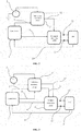
FIG. 1 shows an invention diagram comprising a multi-source distribution circuit (3) connected to an external source (2), to a control unit (1) and to a decoupled output stage circuit (4). -
FIG. 2 shows an invention diagram where an analogue-to-digital converter [ADC] (5) is connected to the decoupled output stage circuit (4), which enables feedback to the control unit (1). -
FIG. 3 shows an invention diagram where the external source (2) is a dual source, in an embodiment of the invention. -
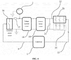
FIG. 4 shows a diagram for the multi-source distribution circuit (3), comprising a control unit (1) connected to a controlled switch circuit (16) and to a source output selector (20), in an embodiment of the invention. The controlled switch circuit (16) is connected to a voltage regulator circuit (18), which is connected to a current limiter (19). -
FIG. 5 shows a diagram for the multi-source distribution circuit (3) where the external source (2) is a dual source, i.e. it bears positive and negative values, in an embodiment of the invention. -
FIG. 6 shows a diagram for the multi-source distribution circuit (3) as having a dual switched source, in an embodiment of the invention. -
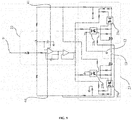
FIG. 7 shows the multi-source distribution circuit (3) used in this invention, in an embodiment of the invention. -
FIG. 8 shows a diagram for the decoupled output stage circuit (4), consisting of an amplification stage circuit (22) connected to an optical decoupling stage circuit (23), in an embodiment of the invention. -
FIG. 9 shows the decoupled output stage circuit (4), consisting of an amplification stage (22), based on operational amplifiers, which is connected to an optical decoupling stage circuit (23), based on optocouplers, in an embodiment of the invention. -
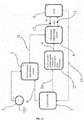
FIG. 10 shows a diagram of the invention where and input/output I/O interface (24) is connected to the control unit (1), which allows the user to interact with the device. -
FIG. 11 shows a diagram of the invention where a signal generator (27) is connected to the control unit (1) and the decoupled output stage circuit (4), in an embodiment of the invention. -
FIG. 12 shows a diagram of the invention where the external source (2) us a dual source and a signal generator (27) is connected to the control unit (1) and the decoupled output stage circuit (4), in an embodiment of the invention. -
FIG. 13 shows a diagram of the invention where the control unit (1) is connected to an output controlling circuit (30), which is connected to an actuator interface (31), in an embodiment of the invention. -
FIG. 14 shows a diagram of the invention where the control unit (1) is connected to an output controlling circuit (30), which is connected to an actuator interface (31), in an embodiment of the invention. In addition, the external source (2) is a dual source. -
FIG. 15 shows a diagram of the invention where the control unit (1) is connected to an output controlling circuit (30) and to a signal generator (27); the output controlling circuit (30) is connected to an actuator interface (31), in an embodiment of the invention. -
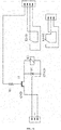
FIG. 16 shows a relay circuit, consisting of a transistor connected to a relay, with control using switches. -
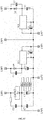
FIG. 17 shows a circuit for an external source (2), consisting of a rectification stage connected to a regulation stage. - This invention is related to an electrical and magnetic tissue stimulation device comprising a multi-source distribution circuit (3), a decoupled output stage circuit (4) connected to the multi-source distribution circuit (3) and to a control unit; the control unit (1) is connected to the multi-source distribution circuit (3) and to the decoupled output stage circuit (4), wherein the control unit (1) generates PE (12) and Out (13) outputs for electrical and magnetic stimulation of a tissue.
- Referring to
FIG. 1 , there is an external source (2) that allows DC or AC power. A multi-source distribution circuit (3) is connected to the external source (2) and to a control unit (1). The purpose of the control unit (1) consists of selecting the multi-source distribution (see explanation below) and of managing stimulation signals (9) targeted to a decoupled output stage circuit (4), either with electrical or magnetic stimulation for the spot to be stimulated. - The decoupled output stage circuit (4) is connected in turn to the multi-source distribution circuit (3) and to the control unit (1). The control unit (1) sends stimulation signals (9). The decoupled output stage circuit (4) has two outputs, PE (12) and Out (13). A transducer is connected to PE (12) and Out (13) outputs. In order to understand this invention, transducer, actuator, motors, electrodes, photo-electrical items, induction actuators, heat generators, resistors, coils are understood to generate magnetic fields by induction, Peltier cells, antennas, or combinations thereof.
- There are different types of stimulation, such as those made up by the group of electrical, magnetic, capacitive, inductive, thermal, vibrational, or photo-electrical stimulation, or a combination thereof.
- In an embodiment of the invention, and referring to
FIG. 2 , there is an external source (2) connected to the multi-source distribution circuit (3). The multi-source distribution circuit (3) is in turn connected to a control unit (1) and to the decoupled output stage circuit (4). - The decoupled output stage circuit (4) is connected through PE (12) and Out (13) outputs to an analogue-to-digital converter [ADC] (5), which sends the digitalized signal (9) from PE (12) and Out (13) channel to the control unit (1). The control unit (1) through the variations existing in PE (12) and Out (13) makes decisions to feedback the decoupled output stage circuit (4) with different stimulation signals (9). Typically, these variations depend on the variation in the load of electrodes by each one of PE (12) and Out (13) channels.
- That is, when a tissue is connected at these spots, the impedance of the stimulated tissue changes, and by changing its impedance through the analogue-to-digital converter [ADC] (5), variations of current and voltage are monitored. With these variations of current and voltage, changes in connected impedance are monitored. Depending upon the change in impedance, the control unit (1) changes the electrical stimulation signal (9).
- This form of decoupled output stage circuit (4) makes a different stimulation to the concerning tissue. For the case of
FIG. 2 , the multi-source distribution circuit has a v. Out (32) output. The external source (2) of stimulation is either positive or negative. - Referring to
FIG. 3 , the external source (2) is a positive/negative source, i.e. a dual source, connected to the multi-source distribution circuit (3). The multi-source distribution circuit (3) is connected to the control unit (1), which selects outputs for the multi-source distribution circuit (3). In this manner, multi-source distribution circuit (3) enables positive v. Out (10), negative v. Out (11), positive output and negative output, in both quadrants, dual or taking the entire range between positive and negative, with zero crossing, i.e. there are signals at zero. - The multi-source distribution circuit (3) is connected to the decoupled output stage circuit (4), through positive v. Out (10), negative v. Out (11) outputs, to carry out stimulation to the desired tissue. The decoupled output stage circuit (4) is connected to an analogue-to-digital converter [ADC] (5) to provide feedback (14) to the control unit (1).
- In an embodiment of the invention, and referring to
FIG. 4 , the multi-source distribution circuit (3) consists of a controlled switch circuit (16) commanded by the control unit (1), through a source control line (6). The controlled switch circuit (16) has an impedance (17) that helps to prevent a short circuit when the controlled switch circuit (16) is closed. - The controlled switch circuit (16) is connected to a voltage regulator (18) and the external source (2). The voltage regulator circuit (18) is selected by the control unit (1) when the controlled switch circuit (16) is closed. In this way, the external source (2) is selected as input. The voltage regulator circuit (18) regulates the external source (2) located at input. A current limiter circuit (19) is connected to the output of the voltage regulator circuit (18). The current limiter circuit (19) keeps the current flow and voltage constant, regardless of impedance changes within a range, and delivers the signal to a output Cp capacitor. (21).
- At the end, the output Cp capacitor (21) is connected to a capacitor bank (33) in parallel. The capacitor bank (33) allows to have capacitors of the same capacity or capacitors of different capacity. Capacitors of the capacitor bank (33) are switched through a source output selector (20), commanded by the control unit (1) through an output control line (15). The capacitor bank (33) has "n" capacitors connected in parallel from a natural "n" number greater than zero from a C1 capacitor to a Cn capacitor. Outputs of the source output selector (20) activate or inactivate each capacitor of the capacitor bank (33).
- Referring to
FIG. 4 andFIG. 7 , in an embodiment of the present invention, the controlled switch circuit (16) consists of: - an integrated circuit with optocoupler (16a) with first optocoupler (47), second optocoupler (48), third optocoupler (49), and forth optocoupler (50);
- the anode of the first optocoupler (47) and the anode of the fourth optocoupler (50) are connected;
- the cathode of the second optocoupler (48) and the cathode of the third optocoupler (49) are connected;
- the cathode of the first optocoupler (47) connected to one terminal of resistive impedance, the other terminal of said resistive impedance connected to the high source control signal (7);
- the cathode of the forth optocoupler (50) connected to one terminal of resistive impedance, the other terminal of said resistive impedance connected to the high source control signal (7);
- the anode of the second optocoupler (48) connected to one terminal of resistive impedance, the other terminal of said resistive impedance connected to the high source control signal (7);
- the anode of the third optocoupler (49) connected to one terminal of resistive impedance, the other terminal of said resistive impedance connected to the high source control signal (7);
- the emitter of the first optocoupler (47) connected to the collector of the second optocoupler (48);
- the emitter of the third optocoupler (49) connected to the collector of the fourth optocoupler (50);
- the collector of the first optocoupler (47) connected with a first high protection impedance (57), the other terminal of said high protection impedance (57) connected to the collector of the third optocoupler (49);
- the emitter of the second optocoupler (48) connected to a second high protection impedance (58).
- Referring to
FIG. 4 , the controlled switch circuit (16) is selected from the group formed by relay circuits, optocouplers, controlled selectors, breakers, transistors, or combinations thereof. - The voltage regulator circuit (18) is selected from the grouped formed by integrated circuits, Zener diodes, circuit with capacitors, circuits with coils, circuits with transistors, electromechanical regulators, or combinations thereof.
- The current limiter circuit (19) is selected from the grouped formed by integrated circuits, circuits with diodes, circuits with transistors, circuits with capacitors and resistors, circuits with coils and resistors, or combinations thereof.
- In a non-illustrated embodiment of this invention, the capacitor bank (33) is connected at the end that is not connected to a source output selector (20), a second source output selector that allows connecting in series and/or in parallel each one of the capacitors of the capacitor bank (33).
- The output control (15) which is commanded by the control unit (1), switches the capacitors of the capacitor bank (33), which are connected in parallel with the output capacitor Cp (21). The output capacitor Cp. (21) is connected to the current limiting circuit (19). The equivalent capacitor between the capacitor bank (33) and the output capacitor Cp (21) is connected to the V. Out output (32). When a capacitor in the capacitor bank (33) that is in parallel with the output capacitor Cp (21) is switched, the amount of output load changes.
- In an embodiment of the invention and referring to
FIG. 5 , the multi-source distributor circuit (3) works for both positive sources (41) and negative sources (40). In this way, a control unit (1) is connected to a controlled switch circuit (16) through a source control line (6). The controlled switch circuit (16) is connected to an impedance (17) that helps prevent a short circuit when the controlled switch circuit (16) is closed. - The controlled switch circuit (16) is connected to a voltage regulator (18) and the positive external source (41). The voltage regulator circuit (18) is selected by the control unit (1) when the controlled switch circuit (16) is closed, in this way, the external source (41) is selected as input. The voltage regulator circuit (18) regulates the external source (41) selected as input. A current limiter circuit (19) is connected to the output of the voltage regulator circuit (18). The current limiter circuit (19) keeps the current flow and voltage constant, regardless of impedance changes within a range, and delivers the signal to a output Cp capacitor. (21).
- At the end, the output Cp capacitor (21) is connected to a capacitor bank (33) in parallel. Capacitors of the capacitor bank (33) are commuted through a source output selector (20), regulated by the control unit (1) through an output control line (15).
- The output control (15) that is commanded by the control unit (1) switches the capacitors that are in parallel of the capacitor bank (33) with the output Cp capacitor (21), which is connected to the current limiter circuit (19). The equivalent capacitor between the capacitor bank (33) and the output capacitor Cp (21) is connected to the positive V. Out (10) output. When connecting at least one capacitor in the capacitor bank (33) that are in parallel with the output Cp capacitor (21), the amount of output load changes.
- In turn, the control unit (1) is connected to a controlled switch circuit (34) through a source control line (6). The controlled switch circuit (34) is connected to an impedance (35) that helps prevent a short circuit when the controlled switch circuit (34) is closed. The controlled switch circuit (34) is connected to a voltage regulator (36) and the positive external source (40).
- The voltage regulator circuit (36) is selected by the control unit (1) when the controlled switch circuit (34) is closed, in this way, the negative source (40) is selected as input. The voltage regulator circuit (36) regulates the negative external source (40) selected as input. A current limiter circuit (37) is connected to the output of the voltage regulator (36) circuit. The current limiter circuit (37) keeps the current flow and voltage constant, regardless of impedance changes within a range, and delivers the signal to a output Cp capacitor (38).
- At the end, the output Cp capacitor (38) is connected to a capacitor bank (39) in parallel. Capacitors of the capacitor bank (39) are switched through a source output selector (42), commanded by the control unit (1) through an output control line (15).
- The capacitor bank (39) has "n" capacitors connected in parallel from a natural "n" number greater than zero from a C1 capacitor to a Cn capacitor; the outputs of the second source output selector (42) activate or inactivate each capacitor of the capacitor bank (39).
- In a non-illustrated embodiment of this invention, the capacitor bank (39) is connected at the end that is not connected to a source output selector (42), a second source output selector that allows connecting in series and/or in parallel each one of the capacitors of the capacitor bank (39).
- The output control (15) that is commanded by the control unit (1) switches the capacitors that are in parallel of the capacitor bank (39) with the output Cp capacitor (38), which is connected to the current limiter circuit (37). The equivalent capacitor between the capacitor bank (39) and the output capacitor Cp (38) are connected to the negative V. Out (11) output. When connecting at least one capacitor in the capacitor bank (39) that are in parallel with the output Cp capacitor (38), the amount of output load changes.
- In an embodiment of the invention and referring to
FIG. 6 , the multi-source distributor circuit (3) works for both positive sources (41) and negative sources (40). - In this way, a control unit (1) is connected to a controlled switch circuit (16) through a source control line (6). The controlled switch circuit (16) has an impedance (17) that helps to prevent a short circuit when the controlled switch circuit (16) is closed. The controlled switch circuit (16) is connected to a voltage regulator (18) and the external positive source (41). The voltage regulator circuit (18) is selected by the control unit (1) when the controlled switch circuit (16) is closed, in this way, the external source (41) is selected as input. The voltage regulator circuit (18) regulates the external source (41) selected as input.
- At the output of the voltage regulator circuit (18), a source output selector (20) is connected, the function of the source output selector (20) is to convert the positive external source (41) to a switched source, this allows greater stability in current and voltage. A current limiter circuit (19) is connected to the output of the source output selector (20). The current limiter circuit (19) keeps the current flow and voltage constant, regardless of impedance changes within a range, and delivers the signal to a output Cp capacitor (21).
- At the end, the output Cp capacitor (21) is connected to a capacitor bank (33) in parallel. Capacitors of the capacitor bank (33) are switched through a source output selector (20), commanded by the control unit (1) through an output control line (15). The output control (15) that is commanded by the control unit (1) connects at least one capacitor in parallel to the capacitor bank (33) with the output Cp capacitor (21), which is connected to the current limiter circuit (19). The equivalent capacitor between the capacitor bank (33) and the output capacitor Cp (21) is connected to the positive V. Out (10) output. When connecting at least one capacitor in the capacitor bank (33) that are in parallel with the output Cp capacitor (21), the amount of output load changes.
- In turn, the control unit (1) is connected to a controlled switch circuit (34) through a source control line (6). The controlled switch circuit (34) is connected to an impedance (35) that helps prevent a short circuit when the controlled switch circuit (34) is closed. The controlled switch circuit (34) is connected to a voltage regulator (36) and the positive external source (40). The voltage regulator (36) circuit is selected by the control unit (1) when the controlled switch circuit (34) is closed. In this way, the negative source (40) is selected as input. The voltage regulator circuit (36) regulates the external source (40) selected as input.
- At the output of the voltage regulator circuit (18), a source output selector (42) is connected, the function of the source output selector (42) is to convert the negative external source (40) to a switched source, this allows greater stability in current and voltage. At the output of the source output selector (42). A current limiter circuit (37) is connected to the output of the source output selector (36). The current limiter circuit (37) keeps the current flow and voltage constant, regardless of impedance changes within a range, and delivers the signal to a output Cp capacitor (38).
- At the end, the output Cp capacitor (38) is connected to a capacitor bank (39) in parallel. Capacitors of the capacitor bank (39) are switched through a source output selector (42), commanded by the control unit (1) through an output control line (15).
- The output control (15) that is commanded by the control unit (1) connects at least one capacitor in parallel to the capacitor bank (39) with the output Cp capacitor (38), which is connected to the current limiter circuit (37). The equivalent capacitor between the capacitor bank (39) and the output capacitor Cp (38) are connected to the output negative V. Out (11). When switching at least one capacitor in the capacitor bank (39) that are in parallel with the output Cp capacitor (38), the amount of output load changes.
- In an embodiment of the invention, and referring to
FIG. 7 , there is a circuit for the multi-source distribution circuit (3). The circuit has an external source (2), which can be, for example, 5 volts, a positive external source (41) and a negative external source (40). - The controlled switch circuit (16) consists of four optocouplers, which are connected in pairs in parallel, to switch the positive external source (41). The external source (2) is connected to a resistive impedance (55). The resistive impedance (55) is connected to the input of two optocouplers, specifically optocouplers (47) and (50). At the input of the other pair of optocouplers, specifically (48) and (49), the high source control signal (7) is connected. Each of the optocouplers is duly protected by a limiting impedance.
- When the control unit (1) sends a control signal, through a high source control line (7), a pair of optocouplers starts to conduct; when this signal is changed, the other pair starts to conduct. Each of the optocouplers has an input to impedance that has the function of limiting the current for the LED diode of each optocoupler.
- To prevent a short circuit when the control unit (1) sends a signal (9), through a high source control line (7), so as not to select the positive external source (41), two resistive impedances (57) and (58) are connected.
- At the output of the controlled switch circuit (16), a voltage regulator circuit (18) is connected. The voltage regulator circuit (18) consists of two Zener diodes. The Zener diode (18a) is connected in parallel with the optocoupler (47) and in series with the optocoupler (48) and the Zener diode (18b) is connected in parallel with the optocoupler (50) and in series with the optocoupler (49). A current limiter circuit (19) is connected to the output of the voltage regulator circuit (18). Each of the optocouplers is duly protected by a limiting impedance.
- The current limiting circuit (19) consists of two MOSFET transistors. MOSFET transistors have their own protection diode. The p-channel MOSFET transistor (19a) is connected to the positive external source (41) through the Source pin. The transistor (19a) is connected to the positive V. Out (10) output and to the output Cp capacitor (21), through the Drain pin. At the transistor Gate pin (19a), the optocouplers (47) and (48) are simultaneously connected.
- The n-channel MOSFET transistor (19b) is connected through its Drain and Source pins, to the circuit reference, i.e. GND In turn, the Gate pin of the transistor (19b) is simultaneously connected to the optocouplers (49) and (50); and in turn, to the Source pin, a decoupling capacitor (C4) is connected, which allows the input source and the output impedance to be decoupled. Transistors (19a) and (19b) keep the current constant, despite changes in impedance. The current limiter circuit (19) is connected to an output Cp capacitor (21).
- The output Cp capacitor (21) is connected in parallel to a capacitor bank (33). In addition, a decoupling capacitor is connected to the output Cp capacitor (21). To connect at least one capacitor from the capacitor bank (33), the control unit (1) sends a signal (9) and switches the source output selector (20). The source output selector (20) connects at least one capacitor from the capacitor bank (33) in parallel with the output Cp capacitor (21), which is in turn connected to the positive V. Out (10) output.
- The parallel between the output Cp capacitor (21) and at least one of the capacitors from the capacitor bank (33) allows to vary the output load.
- The controlled switch circuit (34) consists of four optocouplers, which are connected in pairs in parallel, to switch the negative external source (40). The 5-volt external source (2) is connected to a resistive impedance (56). The resistive impedance (56) is connected to the input of two optocouplers, specifically optocouplers (51) and (54). At the input of the other pair of optocouplers, specifically (52) and (53), the low source control signal (8) is connected.
- When the control unit (1) sends a control signal, through a low source control line (8), a pair of optocouplers starts to conduct; when this signal changes, the other pair of optocouplers starts to conduct. Each of the optocouplers has an input to impedance that has the function of limiting the current for the LED diode of each optocoupler.
- To prevent a short circuit when the control unit (1) sends a signal (9), through a low source control line (8), so as not to select the negative external source (40), two resistive impedances (59) and (60) are connected.
- At the output of the controlled switch circuit (34), a voltage regulator circuit (36) is connected. The voltage regulator circuit (36) consists of two Zener diodes. The Zener diode (36b) is connected in parallel with the optocoupler (51) and in series with the optocoupler (52) and the Zener diode (36a) is connected in parallel with the optocoupler (54) and in series with the optocoupler (53). A current limiter circuit (37) is connected to the output of the voltage regulator circuit (36).
- The current limiting circuit (37) consists of two MOSFET transistors. MOSFET transistors have their own protection diode. The n-channel MOSFET transistor (37b) is connected to the negative external source (40) through the Source pin. The transistor (37b) is connected to the negative V. Out (11) output and to the output Cp capacitor (38), through the Drain pin. At the transistor Gate pin (37b), the optocouplers (53) and (54) are simultaneously connected.
- The p-channel MOSFET transistor (37a) is connected through its Drain and Source pins to the circuit reference, i.e. GND. In turn, the transistor Gate pin (37a) is simultaneously connected to the optocouplers (51) and (52). Transistors (37a) and (37b) keep the current constant, despite changes in impedance. The current limiter circuit (37) is connected to an output Cp capacitor (38).
- The output Cp capacitor (38) is connected in parallel to a capacitor bank (42). To connect at least one capacitor from the capacitor bank (42), the control unit (1) sends a signal (9) and switches the source output selector (39). The source output selector (39) connects at least one capacitor from the capacitor bank (42) in parallel with the output Cp capacitor (38), which is in turn connected to the negative V. Out (11) output.
- The parallel between the output Cp capacitor (38) and at least one of the capacitors from the capacitor bank (39) allows to vary the output load.
- Referring to
FIG. 8 , the signal (9) is commanded by the control unit (1), typically, this signal (9) is a pulse train, where the amplitude, frequency, or pulse step (i.e. how wide the pulse is) are varied. Different results are obtained by changing these features of the signal (9). - The signal (9) comes from a control unit (1), which is a micro-controller, a computer, or a signal generator. Impulsive signals have low power, therefore, in order to deliver it at a greater load, it should be conditioned with an amplification stage circuit (22).
- The signal (9) provided by a control unit (1) enter an amplification stage circuit (22). The output of said amplification stage (22), for security, does not connect transducers directly to the desired tissue. Thus, a decoupling circuit becomes necessary. The decoupling circuit allows for capacitive decoupling, decoupling by transformer, or as shown in
FIG. 8 , an optical decoupling stage circuit (23) in an embodiment of the invention. - The output of the amplification stage circuit (22), the positive V. Out (10) output and the negative V. Out (11) output of the source distributor circuit are connected to the optical decoupling stage circuit (23), from the multi-source distribution circuit (3). At the outputs of the optical decoupling circuit (23), PE (12) and Out (13), the impedance (i.e. the desired tissue) is connected through a transducer. PE (12) and Out (13) outputs are the outputs of the decoupled output stage circuit (4).
- When the impulsive signal (9) enters the optical decoupling stage circuit (23), it switches to the frequency of the impulsive signal (9) sent by the control unit (1) and with the amplitude sent by the control unit (1).
- In an embodiment of the invention and referring to
FIG. 9 , the signal (9), commanded by the control unit (1), is connected to an amplification stage circuit (22). The amplification stage circuit (22) consists of an instrumentation amplifier, which is in turn made up of two operational amplifiers, where the first operational amplifier works as an inverting amplifier, and the second operational amplifier has the function of decoupling impedances. - The output of the amplification stage circuit (22) is connected to an optical decoupling stage circuit (23). The optical decoupling stage circuit (23) consists of a pair of optocouplers for the positive input source (41), which are arranged at the output of the amplification stage circuit (22), with their respective resistive impedance.
- One of these optocouplers, specifically optocoupler (23c), protects the circuit segment for the negative external source (40) when the impulsive signal (9) switches the positive external source (41). Moreover, the second optocoupler integrated circuit (34a) is switched to connect the positive external source (41) to the segment of the circuit having a Zener diode, a resistive impedance and a MOSFET transistor, in order to condition the output signal. This output signal is sent through the PE (12) and Out (13) outputs.
- The optical decoupling stage circuit (23) also has a pair of optocouplers for the negative input source (40), which are arranged at the output of the amplification stage circuit (22), with their respective resistive impedance.
- One of these optocouplers, specifically optocoupler (23d), protects the circuit segment for the negative external source (41) when the impulsive signal (9) switches the negative external source (40). Moreover, the first optocoupler integrated circuit (16a) is switched to connect the negative external source (40) to the segment of the circuit having a Zener diode, a resistive impedance and a MOSFET transistor, in order to condition the output signal. This output signal is sent through the PE (12) and Out (13) outputs.
- PE (12) and Out (13) outputs are connected at the output of the optical decoupling stage (23), where transducers are directly connected.
- Transducers receive the positive V. Out (10) and negative V. Out (11) signals, modulated by the signal amplified by the amplification stage circuit (22). Depending upon the type of transducer, the requirement of the input source changes, therefore, it is necessary to change the load connected to the multi-source distribution circuit (3).
- Referring to
FIG. 10 ; the control unit (1) has a user interface or I/O input and output interface (24), which is a computing device with a display screen, an LCD, a monitor to display feedback (14) being delivered by the analog-to-digital converter [ADC] (5) to the control unit (1), in order to observe the behavior of the impedance connected at PE (12) and Out (13) spots of the decoupled output stage circuit (4). - The user interface or I/O input and output interface (24) allows an expert user to send orders to the control unit (1) to change the features of the signal (9) that the control unit (1) must send to the decoupled output stage circuit (4).
- The control unit (1) is in turn connected to the multi-source distribution circuit (3) to send orders on which input source is to be used. The distributor circuit is connected to a dual positive/negative external source (2). Outputs of the multi-source distribution circuit (3)-positive V. Out (10) and negative V. Out (11)-are connected to the decoupled output stage circuit (4). Outputs of the decoupled output stage circuit (4)-PE (12) and Out (13)-are connected to an analog-to-digital converter [ADC] (5), which sends a feedback signal (14) to the control unit (1).
- Referring to
FIG. 11 , the multi-source distribution circuit (3) is connected to an external source (2) that is positive or negative, and to the control unit (1) through a source control line (6). The control unit (1) is connected to a signal generator (27), through a signal control line (26). The signal generator (27) sends the signal (9) to the decoupled output stage circuit (4). The decoupled output stage circuit (4) receives the signal (9) sent by the signal generator (27) and the V. Out (32) signal sent by the multi-source distribution circuit (3). - Outputs of the decoupled output stage circuit (4)-PE (12) and Out (13)-are connected to an analog-to-digital converter [ADC] (5), which sends a feedback signal (14) to the control unit (1) for monitoring the behavior of the impedance connected to PE (12) and Out (13).
- Referring to
FIG. 12 , the multi-source distribution circuit (3) is connected to a dual positive/negative external source (2) and to the control unit (1) through the high source control line (7) and the low source control line (8). The control unit (1) is connected to a signal generator (27), through a signal control line (26). The signal generator (27) sends the signal (9) to the decoupled output stage circuit (4), which in turn receives the positive V. Out (10) signal and the negative V. Out (11) signal sent by the multi-source distribution circuit (3). - Outputs of the decoupled output stage circuit (4)-PE (12) and Out (13)-are connected to an analog-to-digital converter [ADC] (5), which sends a feedback signal (14) to the control unit (1) for monitoring the behavior of the impedance connected to PE (12) and Out (13) channels.
- Referring to
FIG. 13 , the multi-source distribution circuit (3) is connected to an external source (2) that is positive or negative, and to a control unit (1) through a source control line (6). The control unit (1) is connected to a signal generator (27). The signal generator (27) sends two or more signals (9) to two or more decoupled output stage circuits (4). The signal (9) sent by the signal generator (27) and the V. Out signal (32) sent by the multi-source distribution circuit (3) enter the decoupled output stage circuits (4). Each output stage circuit is connected through the PE (12) and Out (13) outputs to an analog-to-digital converter [ADC] (5), which sends a feedback signal (14) to the control unit (1), for monitoring. - All PE (12) and Out (13) outputs of each decoupled output stage circuit (4) are connected to an output controlling circuit (30). The output controlling circuit (30) receives a signal commanded by the control unit (1), which allows to choose which transducer is to be stimulated. An actuator interface (31) is connected at the output of the output controlling circuit (30). Two or more transducers are connected to the actuator interface (31), through the PE'(43) and Out' (44) outputs.
- Referring to
FIG. 14 , the multi-source distribution circuit (3) is connected to a dual positive/negative external source (2) and to a control unit (1) through a high source control line (7) and a low source control line (8), which allows to switch between positive source and negative source. The control unit (1) sends two or more signals (9) to two or more decoupled output stage circuits (4). - The signal (9) sent by the control unit (1), the positive V. Out signal (10) and the negative V. Out signal (11) sent by the multi-source distribution circuit (3) enter the uncoupled output stage circuits (4). Each output stage circuit is connected through the PE (12) and Out (13) outputs to an analog-to-digital converter [ADC] (5), which sends a feedback signal (14) to the control unit (1), for monitoring.
- All PE (12) and Out (13) outputs of each decoupled output stage circuit (4) are connected to an output controlling circuit (30). The output controlling circuit (30) receives a signal commanded by the control unit (1), which allows to choose which transducer is to be stimulated. An actuator interface (31) is connected at the output of the output controlling circuit (30). Two or more transducers are connected to the actuator interface (31), through the PE'(43) and Out' (44) outputs.
- Referring to
FIG. 15 , the multi-source distribution circuit (3) is connected to a dual positive/negative external source (2) and to a control unit (1) through a high source control line (7) and a low source control line (8), which allows to switch between positive source and negative source. The control unit (1) is connected to a signal generator (27). The signal generator (27) sends two or more signals. - The signal (9) sent by the signal generator (27), the positive V. Out signal (10) and the negative V. Out signal (11) sent by the multi-source distribution circuit (3) enter the uncoupled output stage circuits (4). Each output stage circuit is connected through the PE (12) and Out (13) outputs to an analog-to-digital converter [ADC] (5), which enables feedback (14) to the control unit (1), for monitoring.
- All PE (12) and Out (13) outputs of each decoupled output stage circuit (4) are connected to an output controlling circuit (30). The output controlling circuit (30) receives a signal commanded by the control unit (1), which allows to choose which transducer is to be stimulated. An actuator interface (31) is connected at the output of the output controlling circuit (30). Two or more transducers are connected to the actuator interface (31), through the PE'(43) and Out' (44) outputs.
- Referring to
FIG. 16 , it shows an example of relay circuit. Relay circuit consists of a pair of switches that allow to select whether a transistor starts to conduct or not. When the transistor starts to conduct allows the relay coil to be connected to GND, thus changing the relay's state. - Referring to
FIG. 17 , it shows a circuit for a dual source of 12 volts and -12 volts. This circuit consists of a rectifier, filter and regulators of 12 volts and -12 volts. The segment of the rectification circuit comprises two diodes, a group of resistances and capacitors. After the rectification stage are two stages, which depend upon the voltage; if it is positive, it goes through a voltage regulator of 12 Volts. If the rectified voltage is negative, it goes through a voltage regulator of -12 Volts. - In a non-illustrated embodiment of the invention, the multi-source distribution circuit comprises a control unit (1) connected to a source output selector (20). A voltage regulator circuit (18) is connected to a current limiter (19). The current limiter (19) is connected to a capacitor (21), to a capacitor bank (33) and to the source output sector (20), wherein the control unit (1) controls the source output selector (20) by means of an output control signal bus (15), the source output selector (20) connects or disconnects one or more capacitors from the capacitor bank (33).
- Optionally, in the multi-source distribution circuit, the computing unit (1) is connected to a controlled switch circuit (16). The controlled switch circuit (16) is connected to the voltage regulator circuit (18) and to an impedance (17), which is connected to the voltage regulator circuit (18) and to the controlled switch circuit (16). Wherein the control unit (1) controls the controlled switch circuit (16) by means of a source control signal (6).
- Alternatively, in the multi-source distribution circuit, the computing unit (1) is connected to a second controlled switch circuit (34) connected to a second voltage regulator circuit (36) and to a second impedance (35); the second impedance (35) connected to the second voltage regulator circuit (36) and the second controlled switch circuit (34), the second voltage regulator circuit (36) is connected to a second current limiter (37), which is connected to a second capacitor (38), a second capacitor bank (39) and the source output selector (42);
- wherein the control unit (1) controls the opening and closing of the second controlled switch circuit (34) through the source control signal (6) and controls the second source output selector (42) through the output control signal (15).
- Also, in an embodiment of this invention, for example, the multi-source distribution circuit, the computing unit (1) is connected to a third source output selector (63) connected to the first current limiter (19) and to the first voltage regulator (18). A fourth source output selector (64) connected to the second current limiter (37) and to the second voltage regulator (36).
- It should be understood that this invention is not limited to the described and illustrated embodiments, and the person trained on the technique will understand that numerous variations and modifications can be made that do not depart from the spirit of the invention, which is only defined by the following claims.
Claims (19)
- An electrical and magnetic tissue stimulation device comprising:- a multi-source distribution circuit (3);- a decoupled output stage circuit (4) connected to the multi-source distribution circuit (3) and to a control unit (1); and- the control unit (1) connected to the multi-source distribution circuit (3) and to the decoupled output stage circuit (4);wherein the control unit (1) generates the PE (12) and Out (13) outputs to electrically and magnetically stimulate a tissue.
- The device of Claim 1, wherein the decoupled output stage circuit (4) is connected to a transducer.
- The device of Claim 1, wherein the decoupled output stage circuit (4) and the control unit (1) are connected to an ADC (5).
- The device of Claim 3, characterized in that the multi-source distribution circuit (3) is dual.
- The device of Claim 1, characterized in that the multi-source distribution circuit (3) comprises:- a control unit (1) connected to a controlled switch circuit (16) and to a source output selector (20);- the controlled switch circuit (16) is connected to a voltage regulator circuit (18) and to an impedance (17);- the impedance (17) connected to the voltage regulator circuit (18) and to the controlled switch circuit (16)- the voltage regulator circuit (18) is connected to a current limiter (19); and- the current limiter (19) is connected to a capacitor (21), to a capacitor bank (33) and to the source output selector (20);wherein the control unit (1) controls the controlled switch circuit (16) by means of a source control signal (6) and controls the source output selector (20) through an output control signal bus (15), the source output selector (20) connects or disconnects one or more capacitors from the capacitor bank (33).
- The device of Claim 5, where the multi-source distribution circuit (3) comprises:- a second controlled switch circuit (34) connected to a second voltage regulator circuit (36) and to a second impedance (35);- the second impedance (35) connected to the second voltage regulator circuit (36) and to the second controlled switch circuit (34);- the second voltage regulator circuit (36) is connected to a second current limiter (37); and- the second current limiter (37) is connected to a second capacitor (38), to a second capacitor bank (39) and to the source output selector (42);wherein the control unit (1) controls the opening and closing of the second controlled switch circuit (34) through the source control signal (6) and controls the second source output selector (42) through the output control signal (15).
- The device of Claim 6, wherein the multi-source distribution circuit (3) comprises:- a third source output selector (63) connected to the first current limiter (19) and to the first voltage regulator (18); and- a fourth source output selector (64) connected to the second current limiter (37) and the second voltage regulator (36);the third source output selector (63) and the fourth source output selector (64) connected to the control unit (1);
- The device of Claim 1, wherein the multi-source distribution circuit (3) comprises:- a first controlled switch circuit (16) connected to a high source control signal (7), a first high protection impedance (57), a second high protection impedance (58), a positive voltage regulator circuit (18), and a positive current limiting circuit (19) are connected to the output of the first controlled switch circuit (16);- the positive current limiter circuit (19) connected to a first capacitor (21);- the first capacitor (21) connected to a first source output selector (20) and to a first capacitor bank (33);- a second controlled switch circuit (34) connected to a low source control signal (8), a first low protection impedance (59), a second low protection impedance (60), a negative voltage regulator circuit (18), and a negative current limiting circuit (18) are connected to the output of the second controlled switch circuit (34);- the positive current limiter circuit (37) connected to a second capacitor (38); and- the second capacitor (38) connected to a second source output selector (42) and to a second capacitor bank (39).
- The device of Claim 5 or Claim 6 or Claim 7 or Claim 8, in which, at the end where the source output selector is not connected, a second source output selector is connected to the capacitor bank.
- The device of Claim 1, wherein the decoupled output stage circuit (4) comprises an amplification stage (22) connected to an optical decoupling stage circuit (23).
- The device of Claim 3, wherein the control unit (1) is connected to an I/O interface (13).
- The device of Claim 3, wherein the control unit (1) is connected to a signal generator (27), and the signal generator (27) is connected to the decoupled output stage circuit (4).
- The device of Claim 12, characterized in that the multi-source distribution circuit (3) is dual.
- The device of Claim 3 or Claim 13, wherein the control unit (1) is connected to an output controller (30), the decoupled output stage circuit (4) is connected to the output controller (30); the output controller (30) is connected to an actuator interface (31), which generates the PE' (43) and Out' (44) signals.
- A multi-source distribution circuit comprising:- a control unit (1) connected to a source output selector (20);- a voltage regulator circuit (18) is connected to a current limiter (19);- the current limiter (19) is connected to a capacitor (21), to a capacitor bank (33) and to the source output selector (20);wherein the control unit (1) controls the source output selector (20) through an output control signal bus (15), the source output selector (20) connects or disconnects one or more capacitors from the capacitor bank (33).
- The multi-source distribution circuit of Claim 15, wherein the computing unit (1) is connected to a controlled switch circuit (16), the controlled switch circuit (16) is connected to the voltage regulator circuit (18) and to an impedance (17), the impedance (17) is connected to the voltage regulator circuit (18) and to the controlled switch circuit (16), wherein the control unit (1) controls the controlled switch circuit (16) by means of a source control signal (6).
- The multi-source distribution circuit of Claim 16, wherein the computing unit (1) is connected to a second controlled switch circuit (34) connected to a second voltage regulator circuit (36) and to a second impedance (35);- the second impedance (35) connected to the second voltage regulator circuit (36) and to the second controlled switch circuit (34);- the second voltage regulator circuit (36) is connected to a second current limiter (37);- the second current limiter (37) is connected to a second capacitor (38), to a second capacitor bank (39) and to the source output selector (42);wherein the control unit (1) controls the opening and closing of the second controlled switch circuit (34) through the source control signal (6) and controls the second source output selector (42) through the output control signal (15).
- The multi-source distribution circuit of Claim 17, wherein the computing unit (1) is connected to a third source output selector (63) connected to the first current limiter (19) and to the first voltage regulator (18); and a fourth source output selector (64) connected to the second current limiter (37) and to the second voltage regulator (36);
- The device of Claim 15 or Claim 16 or Claim 17 or Claim 18, in which, at the end where the source output selector is not connected, a second source output selector is connected to the capacitor bank.
Applications Claiming Priority (2)
| Application Number | Priority Date | Filing Date | Title |
|---|---|---|---|
| CONC2017/0011756A CO2017011756A1 (en) | 2017-11-17 | 2017-11-17 | Electrical and magnetic tissue stimulation device |
| PCT/IB2018/059075 WO2019097488A1 (en) | 2017-11-17 | 2018-11-17 | Device for electrical and magnetic tissue stimulation |
Publications (4)
| Publication Number | Publication Date |
|---|---|
| EP3711812A1 true EP3711812A1 (en) | 2020-09-23 |
| EP3711812A4 EP3711812A4 (en) | 2021-08-18 |
| EP3711812C0 EP3711812C0 (en) | 2025-06-18 |
| EP3711812B1 EP3711812B1 (en) | 2025-06-18 |
Family
ID=66533740
Family Applications (1)
| Application Number | Title | Priority Date | Filing Date |
|---|---|---|---|
| EP18878622.2A Active EP3711812B1 (en) | 2017-11-17 | 2018-11-17 | Device for electrical and magnetic tissue stimulation |
Country Status (7)
| Country | Link |
|---|---|
| US (1) | US11628307B2 (en) |
| EP (1) | EP3711812B1 (en) |
| JP (1) | JP7511472B2 (en) |
| CN (1) | CN111727070B (en) |
| CO (1) | CO2017011756A1 (en) |
| ES (1) | ES3041343T3 (en) |
| WO (1) | WO2019097488A1 (en) |
Families Citing this family (14)
| Publication number | Priority date | Publication date | Assignee | Title |
|---|---|---|---|---|
| US10695575B1 (en) | 2016-05-10 | 2020-06-30 | Btl Medical Technologies S.R.O. | Aesthetic method of biological structure treatment by magnetic field |
| US11266850B2 (en) | 2015-07-01 | 2022-03-08 | Btl Healthcare Technologies A.S. | High power time varying magnetic field therapy |
| US20180001107A1 (en) | 2016-07-01 | 2018-01-04 | Btl Holdings Limited | Aesthetic method of biological structure treatment by magnetic field |
| US11464993B2 (en) | 2016-05-03 | 2022-10-11 | Btl Healthcare Technologies A.S. | Device including RF source of energy and vacuum system |
| US12654023B2 (en) | 2016-05-10 | 2026-06-16 | Btl Medical Solutions A.S. | Aesthetic method of biological structure treatment by magnetic field |
| US11534619B2 (en) | 2016-05-10 | 2022-12-27 | Btl Medical Solutions A.S. | Aesthetic method of biological structure treatment by magnetic field |
| US12558146B2 (en) | 2019-04-11 | 2026-02-24 | Btl Medical Solutions A.S. | Methods and devices for aesthetic treatment of biological structures by radiofrequency and magnetic energy |
| US12611545B2 (en) | 2020-05-04 | 2026-04-28 | Btl Healthcare Technologies A.S. | Device and method for unattended treatment of a patient |
| US11878167B2 (en) | 2020-05-04 | 2024-01-23 | Btl Healthcare Technologies A.S. | Device and method for unattended treatment of a patient |
| HRP20250160T1 (en) | 2020-05-04 | 2025-03-28 | Btl Healthcare Technologies A.S. | DEVICE FOR TREATING PATIENTS WITHOUT THE PRESENCE OF A DOCTOR |
| CN115078836B (en) * | 2020-12-31 | 2025-08-05 | 点奇生物医疗科技(北京)有限公司 | Current excitation device with filtering and current excitation device with impedance matching |
| CA3260012A1 (en) | 2021-10-13 | 2023-04-20 | Btl Medical Solutions A.S. | Devices for aesthetic treatment of biological structures by radiofrequency and magnetic energy |
| CN114451901A (en) * | 2022-02-10 | 2022-05-10 | 苏州景昱医疗器械有限公司 | Brain medical analysis device and control unit |
| US20260097226A1 (en) | 2024-10-08 | 2026-04-09 | Btl Medical Solutions A.S. | Devices and methods for application of a magnetic field to the nervous system |
Family Cites Families (10)
| Publication number | Priority date | Publication date | Assignee | Title |
|---|---|---|---|---|
| GB9402545D0 (en) | 1994-02-10 | 1994-04-06 | Magstim Co Ltd | Magnetic stimulators |
| US5591212A (en) * | 1995-07-21 | 1997-01-07 | Medtronic, Inc. | Hybrid battery for implantable pulse generator |
| US5658322A (en) | 1995-10-11 | 1997-08-19 | Regeneration Technology | Bio-active frequency generator and method |
| AU2002953278A0 (en) | 2002-12-12 | 2003-01-02 | Skop Australia Pty Ltd | Electro stimulation treatment apparatus and method |
| US8423132B2 (en) * | 2002-12-12 | 2013-04-16 | Bio Control Medical (B.C.M.) Ltd. | Efficient dynamic stimulation in an implanted device |
| CN103052424B (en) * | 2010-06-04 | 2015-12-16 | 大学健康网络 | Functional electrical stimulation devices and systems and uses thereof |
| CN103311878B (en) * | 2013-04-24 | 2016-03-02 | 华南理工大学 | A kind of bipolar electrical stimulation protection device |
| CN106794340A (en) * | 2014-07-10 | 2017-05-31 | 米克伦设备有限责任公司 | Circuits for Implantable Devices |
| US10213602B2 (en) * | 2015-01-13 | 2019-02-26 | Theranica Bio-Electronics Ltd. | Treatment of headaches by electrical stimulation |
| US10143840B2 (en) | 2015-02-24 | 2018-12-04 | Elira, Inc. | Systems and methods for enabling appetite modulation and/or improving dietary compliance using an electro-dermal patch |
-
2017
- 2017-11-17 CO CONC2017/0011756A patent/CO2017011756A1/en unknown
-
2018
- 2018-11-17 EP EP18878622.2A patent/EP3711812B1/en active Active
- 2018-11-17 JP JP2020545008A patent/JP7511472B2/en active Active
- 2018-11-17 WO PCT/IB2018/059075 patent/WO2019097488A1/en not_active Ceased
- 2018-11-17 CN CN201880078638.3A patent/CN111727070B/en active Active
- 2018-11-17 US US16/764,530 patent/US11628307B2/en active Active
- 2018-11-17 ES ES18878622T patent/ES3041343T3/en active Active
Also Published As
| Publication number | Publication date |
|---|---|
| ES3041343T3 (en) | 2025-11-11 |
| EP3711812C0 (en) | 2025-06-18 |
| US11628307B2 (en) | 2023-04-18 |
| US20200368545A1 (en) | 2020-11-26 |
| JP2021503355A (en) | 2021-02-12 |
| CN111727070A (en) | 2020-09-29 |
| CO2017011756A1 (en) | 2019-05-21 |
| JP7511472B2 (en) | 2024-07-05 |
| EP3711812B1 (en) | 2025-06-18 |
| WO2019097488A1 (en) | 2019-05-23 |
| EP3711812A4 (en) | 2021-08-18 |
| CN111727070B (en) | 2024-07-05 |
Similar Documents
| Publication | Publication Date | Title |
|---|---|---|
| EP3711812B1 (en) | Device for electrical and magnetic tissue stimulation | |
| US11666774B2 (en) | Pulse source and method for magnetically inductive nerve stimulation | |
| US11697022B2 (en) | Architectures for sharing of current sources in an implantable medical device | |
| US8588927B2 (en) | Implantable pulse generator | |
| JP6118860B2 (en) | Battery management for implantable medical devices | |
| EP2825252B1 (en) | Neurostimulation system for preventing magnetically induced currents in electronic circuitry | |
| Souza et al. | Power amplifier circuits for functional electrical stimulation systems | |
| WO1997036645A2 (en) | Electrotherapy device | |
| DE102013211859A1 (en) | Magnetic stimulator for stimulating a tissue through a magnetic field | |
| US12070602B2 (en) | Method for generating electrical signals and computer-readable medium | |
| EP2635344B1 (en) | Apparatus for energy efficient stimulation | |
| CN106606820B (en) | Electrical stimulation device | |
| CN100415319C (en) | Human-body potential controlling electrotherapeutic device | |
| AU2019398172B2 (en) | Electrical stimulation devices and systems for safely operating such devices | |
| CN112023265B (en) | Electrical stimulation device | |
| CN115671549A (en) | A low power consumption electrical stimulation method and device | |
| CN204543275U (en) | Power supply adjustment circuit of electrotherapy machine | |
| DE10146352B4 (en) | Device for generating electromagnetic waves | |
| Al-Mutawaly et al. | Design and Construction of an Electrical Nerve Stimulator | |
| KR20170055369A (en) | A high frequency electrical stimulator with low frequency electrical effects | |
| UA126219U (en) | DEVICES FOR TREATMENT OF SPINAL BRAIN INJURY | |
| Ikram | A systematic approach to a high-efficiency and displacement-tolerant link design for inductively-powered biomedical implants |
Legal Events
| Date | Code | Title | Description |
|---|---|---|---|
| STAA | Information on the status of an ep patent application or granted ep patent |
Free format text: STATUS: THE INTERNATIONAL PUBLICATION HAS BEEN MADE |
|
| PUAI | Public reference made under article 153(3) epc to a published international application that has entered the european phase |
Free format text: ORIGINAL CODE: 0009012 |
|
| STAA | Information on the status of an ep patent application or granted ep patent |
Free format text: STATUS: REQUEST FOR EXAMINATION WAS MADE |
|
| 17P | Request for examination filed |
Effective date: 20200617 |
|
| AK | Designated contracting states |
Kind code of ref document: A1 Designated state(s): AL AT BE BG CH CY CZ DE DK EE ES FI FR GB GR HR HU IE IS IT LI LT LU LV MC MK MT NL NO PL PT RO RS SE SI SK SM TR |
|
| AX | Request for extension of the european patent |
Extension state: BA ME |
|
| DAV | Request for validation of the european patent (deleted) | ||
| DAX | Request for extension of the european patent (deleted) | ||
| REG | Reference to a national code |
Ref country code: DE Ref legal event code: R079 Free format text: PREVIOUS MAIN CLASS: A61N0001000000 Ipc: A61N0002000000 Ref country code: DE Ref legal event code: R079 Ref document number: 602018082773 Country of ref document: DE Free format text: PREVIOUS MAIN CLASS: A61N0001000000 Ipc: A61N0002000000 |
|
| A4 | Supplementary search report drawn up and despatched |
Effective date: 20210719 |
|
| RIC1 | Information provided on ipc code assigned before grant |
Ipc: A61N 2/00 20060101AFI20210713BHEP Ipc: A61N 1/36 20060101ALI20210713BHEP |
|
| STAA | Information on the status of an ep patent application or granted ep patent |
Free format text: STATUS: EXAMINATION IS IN PROGRESS |
|
| 17Q | First examination report despatched |
Effective date: 20230404 |
|
| REG | Reference to a national code |
Ref country code: DE Ref legal event code: R079 Free format text: PREVIOUS MAIN CLASS: A61N0002000000 Ipc: A61N0001360000 Ref country code: DE Ref legal event code: R079 Ref document number: 602018082773 Country of ref document: DE Free format text: PREVIOUS MAIN CLASS: A61N0002000000 Ipc: A61N0001360000 |
|
| GRAP | Despatch of communication of intention to grant a patent |
Free format text: ORIGINAL CODE: EPIDOSNIGR1 |
|
| STAA | Information on the status of an ep patent application or granted ep patent |
Free format text: STATUS: GRANT OF PATENT IS INTENDED |
|
| INTG | Intention to grant announced |
Effective date: 20241022 |
|
| RIC1 | Information provided on ipc code assigned before grant |
Ipc: A61N 1/04 20060101ALI20241014BHEP Ipc: A61N 2/00 20060101ALI20241014BHEP Ipc: A61N 1/36 20060101AFI20241014BHEP |
|
| GRAS | Grant fee paid |
Free format text: ORIGINAL CODE: EPIDOSNIGR3 |
|
| GRAA | (expected) grant |
Free format text: ORIGINAL CODE: 0009210 |
|
| STAA | Information on the status of an ep patent application or granted ep patent |
Free format text: STATUS: THE PATENT HAS BEEN GRANTED |
|
| AK | Designated contracting states |
Kind code of ref document: B1 Designated state(s): AL AT BE BG CH CY CZ DE DK EE ES FI FR GB GR HR HU IE IS IT LI LT LU LV MC MK MT NL NO PL PT RO RS SE SI SK SM TR |
|
| REG | Reference to a national code |
Ref country code: GB Ref legal event code: FG4D |
|
| REG | Reference to a national code |
Ref country code: CH Ref legal event code: EP |
|
| REG | Reference to a national code |
Ref country code: DE Ref legal event code: R096 Ref document number: 602018082773 Country of ref document: DE |
|
| REG | Reference to a national code |
Ref country code: CH Ref legal event code: EP |
|
| REG | Reference to a national code |
Ref country code: IE Ref legal event code: FG4D |
|
| U01 | Request for unitary effect filed |
Effective date: 20250627 |
|
| U07 | Unitary effect registered |
Designated state(s): AT BE BG DE DK EE FI FR IT LT LU LV MT NL PT RO SE SI Effective date: 20250704 |
|
| PG25 | Lapsed in a contracting state [announced via postgrant information from national office to epo] |
Ref country code: NO Free format text: LAPSE BECAUSE OF FAILURE TO SUBMIT A TRANSLATION OF THE DESCRIPTION OR TO PAY THE FEE WITHIN THE PRESCRIBED TIME-LIMIT Effective date: 20250918 Ref country code: GR Free format text: LAPSE BECAUSE OF FAILURE TO SUBMIT A TRANSLATION OF THE DESCRIPTION OR TO PAY THE FEE WITHIN THE PRESCRIBED TIME-LIMIT Effective date: 20250919 |
|
| PG25 | Lapsed in a contracting state [announced via postgrant information from national office to epo] |
Ref country code: HR Free format text: LAPSE BECAUSE OF FAILURE TO SUBMIT A TRANSLATION OF THE DESCRIPTION OR TO PAY THE FEE WITHIN THE PRESCRIBED TIME-LIMIT Effective date: 20250618 |
|
| PG25 | Lapsed in a contracting state [announced via postgrant information from national office to epo] |
Ref country code: RS Free format text: LAPSE BECAUSE OF FAILURE TO SUBMIT A TRANSLATION OF THE DESCRIPTION OR TO PAY THE FEE WITHIN THE PRESCRIBED TIME-LIMIT Effective date: 20250918 |
|
| REG | Reference to a national code |
Ref country code: ES Ref legal event code: FG2A Ref document number: 3041343 Country of ref document: ES Kind code of ref document: T3 Effective date: 20251111 |
|
| U20 | Renewal fee for the european patent with unitary effect paid |
Year of fee payment: 8 Effective date: 20251105 |
|
| PG25 | Lapsed in a contracting state [announced via postgrant information from national office to epo] |
Ref country code: IS Free format text: LAPSE BECAUSE OF FAILURE TO SUBMIT A TRANSLATION OF THE DESCRIPTION OR TO PAY THE FEE WITHIN THE PRESCRIBED TIME-LIMIT Effective date: 20251018 |
|
| PGFP | Annual fee paid to national office [announced via postgrant information from national office to epo] |
Ref country code: GB Payment date: 20251105 Year of fee payment: 8 |
|
| PG25 | Lapsed in a contracting state [announced via postgrant information from national office to epo] |
Ref country code: SM Free format text: LAPSE BECAUSE OF FAILURE TO SUBMIT A TRANSLATION OF THE DESCRIPTION OR TO PAY THE FEE WITHIN THE PRESCRIBED TIME-LIMIT Effective date: 20250618 |
|
| PG25 | Lapsed in a contracting state [announced via postgrant information from national office to epo] |
Ref country code: CZ Free format text: LAPSE BECAUSE OF FAILURE TO SUBMIT A TRANSLATION OF THE DESCRIPTION OR TO PAY THE FEE WITHIN THE PRESCRIBED TIME-LIMIT Effective date: 20250618 |
|
| PG25 | Lapsed in a contracting state [announced via postgrant information from national office to epo] |
Ref country code: PL Free format text: LAPSE BECAUSE OF FAILURE TO SUBMIT A TRANSLATION OF THE DESCRIPTION OR TO PAY THE FEE WITHIN THE PRESCRIBED TIME-LIMIT Effective date: 20250618 |
|
| PG25 | Lapsed in a contracting state [announced via postgrant information from national office to epo] |
Ref country code: SK Free format text: LAPSE BECAUSE OF FAILURE TO SUBMIT A TRANSLATION OF THE DESCRIPTION OR TO PAY THE FEE WITHIN THE PRESCRIBED TIME-LIMIT Effective date: 20250618 |
|
| PGFP | Annual fee paid to national office [announced via postgrant information from national office to epo] |
Ref country code: ES Payment date: 20251209 Year of fee payment: 8 |
|
| PLBE | No opposition filed within time limit |
Free format text: ORIGINAL CODE: 0009261 |
|
| STAA | Information on the status of an ep patent application or granted ep patent |
Free format text: STATUS: NO OPPOSITION FILED WITHIN TIME LIMIT |
|
| REG | Reference to a national code |
Ref country code: CH Ref legal event code: L10 Free format text: ST27 STATUS EVENT CODE: U-0-0-L10-L00 (AS PROVIDED BY THE NATIONAL OFFICE) Effective date: 20260430 |
|
| 26N | No opposition filed |
Effective date: 20260319 |
|
| REG | Reference to a national code |
Ref country code: CH Ref legal event code: H13 Free format text: ST27 STATUS EVENT CODE: U-0-0-H10-H13 (AS PROVIDED BY THE NATIONAL OFFICE) Effective date: 20260623 |
|
| PG25 | Lapsed in a contracting state [announced via postgrant information from national office to epo] |
Ref country code: MC Free format text: LAPSE BECAUSE OF FAILURE TO SUBMIT A TRANSLATION OF THE DESCRIPTION OR TO PAY THE FEE WITHIN THE PRESCRIBED TIME-LIMIT Effective date: 20250618 |
|
| PG25 | Lapsed in a contracting state [announced via postgrant information from national office to epo] |
Ref country code: CH Free format text: LAPSE BECAUSE OF NON-PAYMENT OF DUE FEES Effective date: 20251130 |