EP3709781A1 - Driver circuit device - Google Patents
Driver circuit device Download PDFInfo
- Publication number
- EP3709781A1 EP3709781A1 EP20161175.3A EP20161175A EP3709781A1 EP 3709781 A1 EP3709781 A1 EP 3709781A1 EP 20161175 A EP20161175 A EP 20161175A EP 3709781 A1 EP3709781 A1 EP 3709781A1
- Authority
- EP
- European Patent Office
- Prior art keywords
- circuit
- external device
- driver
- driver circuit
- gate driver
- Prior art date
- Legal status (The legal status is an assumption and is not a legal conclusion. Google has not performed a legal analysis and makes no representation as to the accuracy of the status listed.)
- Granted
Links
Images







Classifications
-
- H—ELECTRICITY
- H02—GENERATION; CONVERSION OR DISTRIBUTION OF ELECTRIC POWER
- H02M—APPARATUS FOR CONVERSION BETWEEN AC AND AC, BETWEEN AC AND DC, OR BETWEEN DC AND DC, AND FOR USE WITH MAINS OR SIMILAR POWER SUPPLY SYSTEMS; CONVERSION OF DC OR AC INPUT POWER INTO SURGE OUTPUT POWER; CONTROL OR REGULATION THEREOF
- H02M1/00—Details of apparatus for conversion
- H02M1/08—Circuits specially adapted for the generation of control voltages for semiconductor devices incorporated in static converters
-
- H—ELECTRICITY
- H05—ELECTRIC TECHNIQUES NOT OTHERWISE PROVIDED FOR
- H05K—PRINTED CIRCUITS; CASINGS OR CONSTRUCTIONAL DETAILS OF ELECTRIC APPARATUS; MANUFACTURE OF ASSEMBLAGES OF ELECTRICAL COMPONENTS
- H05K5/00—Casings, cabinets or drawers for electric apparatus
- H05K5/02—Details
- H05K5/0247—Electrical details of casings, e.g. terminals, passages for cables or wiring
-
- H—ELECTRICITY
- H03—ELECTRONIC CIRCUITRY
- H03K—PULSE TECHNIQUE
- H03K17/00—Electronic switching or gating, i.e. not by contact-making and –breaking
- H03K17/51—Electronic switching or gating, i.e. not by contact-making and –breaking characterised by the components used
- H03K17/56—Electronic switching or gating, i.e. not by contact-making and –breaking characterised by the components used by the use, as active elements, of semiconductor devices
- H03K17/567—Circuits characterised by the use of more than one type of semiconductor device, e.g. BIMOS, composite devices such as IGBT
-
- H—ELECTRICITY
- H05—ELECTRIC TECHNIQUES NOT OTHERWISE PROVIDED FOR
- H05K—PRINTED CIRCUITS; CASINGS OR CONSTRUCTIONAL DETAILS OF ELECTRIC APPARATUS; MANUFACTURE OF ASSEMBLAGES OF ELECTRICAL COMPONENTS
- H05K5/00—Casings, cabinets or drawers for electric apparatus
- H05K5/0026—Casings, cabinets or drawers for electric apparatus provided with connectors and printed circuit boards [PCB], e.g. automotive electronic control units
- H05K5/0065—Casings, cabinets or drawers for electric apparatus provided with connectors and printed circuit boards [PCB], e.g. automotive electronic control units wherein modules are associated together, e.g. electromechanical assemblies, modular structures
-
- H—ELECTRICITY
- H05—ELECTRIC TECHNIQUES NOT OTHERWISE PROVIDED FOR
- H05K—PRINTED CIRCUITS; CASINGS OR CONSTRUCTIONAL DETAILS OF ELECTRIC APPARATUS; MANUFACTURE OF ASSEMBLAGES OF ELECTRICAL COMPONENTS
- H05K5/00—Casings, cabinets or drawers for electric apparatus
- H05K5/0026—Casings, cabinets or drawers for electric apparatus provided with connectors and printed circuit boards [PCB], e.g. automotive electronic control units
- H05K5/0069—Casings, cabinets or drawers for electric apparatus provided with connectors and printed circuit boards [PCB], e.g. automotive electronic control units having connector relating features for connecting the connector pins with the PCB or for mounting the connector body with the housing
-
- H—ELECTRICITY
- H05—ELECTRIC TECHNIQUES NOT OTHERWISE PROVIDED FOR
- H05K—PRINTED CIRCUITS; CASINGS OR CONSTRUCTIONAL DETAILS OF ELECTRIC APPARATUS; MANUFACTURE OF ASSEMBLAGES OF ELECTRICAL COMPONENTS
- H05K5/00—Casings, cabinets or drawers for electric apparatus
- H05K5/30—Side-by-side or stacked arrangements
-
- H—ELECTRICITY
- H05—ELECTRIC TECHNIQUES NOT OTHERWISE PROVIDED FOR
- H05K—PRINTED CIRCUITS; CASINGS OR CONSTRUCTIONAL DETAILS OF ELECTRIC APPARATUS; MANUFACTURE OF ASSEMBLAGES OF ELECTRICAL COMPONENTS
- H05K7/00—Constructional details common to different types of electric apparatus
- H05K7/14—Mounting supporting structure in casing or on frame or rack
- H05K7/1422—Printed circuit boards receptacles, e.g. stacked structures, electronic circuit modules or box like frames
- H05K7/1427—Housings
- H05K7/1432—Housings specially adapted for power drive units or power converters
- H05K7/14322—Housings specially adapted for power drive units or power converters wherein the control and power circuits of a power converter are arranged within the same casing
Definitions
- the present invention relates to a driver circuit device which drives an external device including a semiconductor element.
- a driver circuit device is typically used for driving a module having a power semiconductor such as IGBT (Insulated Gate-Bipolar Transistor), for instance.
- IGBT Insulated Gate-Bipolar Transistor
- JP5477157B2 discloses a prior art example of a power semiconductor module.
- the power semiconductor module of the prior art example has the following structure. Specifically, semiconductor chips and wiring patterns are mounted on an insulating substrate, and conductors including the wiring patterns are electrically insulated from one another by ceramic layers or insulating layers, and the whole module is packaged with a case to be also insulated from an external part.
- the module terminals which are output-side elements when seen in terms of the relation with a gate driver or the like used in combination with the power semiconductor module need to be surely insulated also from input-side elements of the gate driver.
- the present invention adopts the following configuration. Note that the parenthesized notes in the following description are only for reference and do not limit the present invention.
- a driver circuit device of a first configuration is usable with its circuit board being mounted on a driving-target external device, and the driver circuit device applies, to the external device, a drive signal generated in a driver circuit formed on the circuit board.
- the external device performs the switching of a relatively large current (power generation current, for instance) by using a power semiconductor element such as IGBT, for instance, and when seen in terms of the relation with the driver circuit device, the whole external device is an output side and part of the driver circuit device is an input side. Therefore, the input-side part of the driver circuit device needs to be surely insulated from the external device which is the output side.
- insulation distance a sufficient physical spatial distance
- the driver circuit device of the first configuration has an insulating surrounding member that surrounds a peripheral edge of the circuit board, thereby having a sufficient insulation distance from the external device while a physical spatial distance that should be provided between the driver circuit device and the external device is reduced. Consequently, even in the state where the external device and the driver circuit device are combined, it is possible to reduce the whole size, enabling a space-saving and high-density arrangement.
- a driver circuit device of a second configuration includes a plurality of circuit boards.
- the plurality of circuit boards can be mounted on a driving-target external device with their circuit surfaces facing each other.
- the driver circuit device can be further reduced in its whole mounting area.
- the driver circuit device applies, to an external device, drive signals generated in the driver circuits formed on the plurality of circuit boards. If an input-side circuit is formed on a specific circuit board out of the plurality of circuit boards, the other circuit board is an output side similarly to the external device, and accordingly, the insulation is also necessary between these circuit boards.
- the insulating surrounding member is disposed to surround the peripheral edge of this circuit board. Consequently, a physical spatial distance that should be provided between the driver circuit device and the external device can be reduced yet a sufficient insulation distance can be kept therebetween. Further, even in the state where the external device and the driver circuit device are combined, it is also possible to reduce the whole size, enabling a space-saving and high-density arrangement.
- a partition member can be further disposed between the plurality of circuit boards.
- a physical spatial distance that should be provided therebetween can be reduced, enabling a further reduction in the mounting height (dimension in a stacking direction of the circuit boards) of the driver circuit device.
- the surrounding member and the partition member which are used in the second configuration can be integrated, and in this case, the structure is simplified and molding and assembling are facilitated.
- Embodiments of a driver circuit device will be hereinafter described with reference to the drawings.
- a gate driver is taken as an example of the driver circuit device and an IGBT module is taken as an example of a driving-target external device
- the external device and the gate driver of the embodiments are not limited to these examples, and the external device may be a different power semiconductor module and the gate driver may be in a packaged state.
- FIG. 1A is a perspective view illustrating the configuration of a gate driver 100 of one embodiment
- FIG. IB is a plan view thereof.
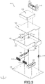
- FIG. 2 and FIG. 3 are exploded perspective views of the gate driver 100.
- the gate driver 100 includes two driver boards 102, 104 which are disposed apart from each other in an up-down direction (Z-axis direction in FIG. 2 and FIG. 3 ).
- a not-illustrated gate driver circuit is formed on the driver boards 102, 104.
- Each of the driver boards 102, 104 itself also has a multilayer structure, and the two driver boards 102, 104 are stacked with their circuit surfaces facing each other. Further, a space is kept between the two driver boards 102, 104, which will be described in more detail with reference to other drawings.
- a DC-DC converter 106 On the driver board 104 (disposed on the upper side in FIG. 1A to FIG. 3 ), a DC-DC converter 106, an input connector 110, and various kinds of not-illustrated chip components are mounted, and besides, not-illustrated wiring patterns are formed. Wiring lines connecting to an external DC power source, a control unit, and so on, which are not illustrated, can be connected to the input connector 110.
- the DC-DC converter 106 converts an externally input DC power (for example, DC +12 V) into a drive current for the gate driver circuit.
- the external power source may be an AC power source, and in this case, an AC-DC converter or the like can be mounted on the driver board 104.
- the two driver boards 102, 104 are coupled with each other, with a plurality of lead pins 112 and support pins 114 therebetween, and out of these, arrays of the lead pins 112 electrically connect the driver boards 102, 104.
- Arrays of the support pins 114 structurally couple the two driver boards 102, 104.
- the arrays of the support pins 114 and the lead pins 112 keep the space between the two driver boards 102, 104.
- the not-illustrated gate driver circuit is formed on the two driver boards 102, 104 as described above, and the gate driver circuit is divided into a plurality of systems according to the circuit configuration (semiconductor bridge) of a driving-target module. How the gate driver circuit drives the semiconductors will be further described in detail later.
- the gate driver 100 further includes an insulating member 120 surrounding the driver board 104.
- the insulating member 120 is formed of, for example, an insulating resin, and its whole shape is like that of a casing covering a lower surface of the driver board 104 while surrounding a peripheral edge of the driver board 104.
- the insulating member 120 includes a pair of flat surface walls 122 and a pair of bent walls 124 each having a shape along the corresponding edge portion of the driver board 104. Such an insulating member 120 is disposed in a state of standing on the circuit surface of the other driver board 102.
- the insulating member 120 further includes a flat plate-shaped division wall 126 in its region covering the lower surface of the driver board 104, and a peripheral edge of the division wall 126 is coupled with inner wall surfaces of the flat surface walls 122 and the bent walls 124. Further, the division wall 126 has openings 128, 129 formed at its appropriate positions, and the aforesaid arrays of the lead pins 112 and the support pins 114 are inserted to the openings 128, 129 respectively. Note that a lower surface, not illustrated in FIG. 2 and FIG. 3 , of the division wall 126 is at a position slightly higher than lower ends of the flat surface walls 122 and the bent walls 124, ensuring that the division wall 126 and an upper circuit surface of the other driver board 102 are spaced.
- a pair of output connectors 108 is mounted and besides, not-illustrated various chip components are mounted.
- the output connectors 108 are disposed at positions outside the insulating member 120, that is, are separated from the driver board 104 by the insulating member 120. Because the edge portions of the driver board 104 and the bent walls 124 are cranked, mounting ranges of the output connectors 108 and an installation range of the insulating member 120 do not interfere with each other on the circuit surface. The use purpose of the output connectors 108 will be further described later.
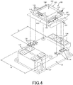
- the gate driver 100 is capable of driving semiconductor elements (IGBT) in the state of being mounted on the driving-target IGBT module 130 as illustrated in FIG. 4 .
- the IGBT module 130 is provided with various kinds of connection terminals 132, 134, 136, and the gate driver 100 is mounted thereon with lower surface terminals (not illustrated) of the driver board 102 press-joined to the connection terminals 136, for instance.
- main conductors (+ and -) such as busbars are connected to the connection terminals 132 which are located on one side of the IGBT module 130 in terms of the longitudinal detection and conductors for midpoint between the semiconductor elements are connected to the connection terminals 134 which are located on the other side.
- a mounting region of the gate driver 100 is reserved in advance, and this mounting region is defined by a dimension L and a dimension W in the longitudinal direction and the width direction of the IGBT module 130 respectively, for instance. Accordingly, the gate driver 100 is structured such that the outside dimension of the driver board 102 falls within the mounting region (dimensions L, W).
- FIG. 5 is a circuit diagram illustrating the connection relation between the gate driver 100 and the IGBT module 130.
- the gate driver 100 When mounted on the IGBT module 130 in the above-described manner, the gate driver 100 is electrically connected with the IGBT module 130 through the connection terminals 136.
- the gate driver 100 includes two gate driver circuits 141, 142 corresponding to the semiconductor elements Q1, Q2 provided in the IGBT module 130 respectively, and the gate driver circuits 141, 142 apply gate drive signals to the semiconductor elements Q1, Q2 through resistors R1, R2 respectively. Note that, when seen from the gate driver 100, the whole IGBT module 130 can be considered as its driving-target external device or only a part corresponding to the semiconductor elements Q1, Q2 can be considered as its driving-target external device.
- control signals are externally input to the gate driver circuits 141, 142 through the input connector 110 (not illustrated in FIG. 5 ), and besides, a DC current is also externally input (supplied) to the DC-DC converter 106.
- the drive current is supplied to the gate driver circuits 141, 142 from the DC-DC converter 106.
- an input-side (primary-side) circuit and an output-side (secondary-side) circuit are electrically insulated, and this input-side circuit PI includes the input connector 110, a not-illustrated primary-side circuit in the DC-DC converter 106, not-illustrated primary-side circuits in the gate driver circuits 141, 142, and their resistors, wiring patterns, connection terminals, and so on.
- the whole IGBT module 130 is an output-side circuit PO when seen in the state where the gate driver 100 is mounted thereon, and the output-side circuit PO at this time includes a not-illustrated secondary-side circuit in the DC-DC converter 106, not illustrated secondary-side circuits in the gate driver circuits 141, 142, and their resistors R1, R2, wiring patterns, connection terminals, and so on which are all insulated from the input-side circuit PI.
- an appropriate insulation distance Id needs to be kept between the input-side circuit PI and the output-side circuit PO, but there are various structural restrictions in keeping the insulation distance Id because the gate driver 100 is structured to be mounted on the package surface of the IGBT module 130 as described above and the gate driver 100 itself needs to be as compact as possible to be reduced in its mounting height and mounting area.
- the aforesaid structural restrictions would oblige a person with an ordinary skill in the art to provide a large spatial distance between the gate driver 100 and the IGBT module 130 or make the mounting height of the gate driver 100 itself large to thereby keep the insulation distance Id.
- the inventors have succeeded in reducing a physical spatial distance between the input-side circuit PI and the output-side circuit PO by suitably disposing the insulating member 120. How the insulation distance Id is kept (the spatial distance is reduced) in the mounted state will be described below.
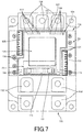
- FIG. 6 and FIG. 7 will be referred to.
- the IGBT module 130 which is a mounting destination is indicated by the two-dot chain line.
- the input-side circuit PI includes the input connector 110, the primary-side circuit of the DC-DC converter 106, the primary-side circuits in the gate driver circuits 141, 142 (not illustrated in FIG. 5 and FIG. 6 ), and so on, and they are structurally disposed in the range indicated by the bold broken line in FIG. 6 and FIG. 7 .
- an insulating element 135 is mounted on the driver board 104, and the dimension (standard dimension) of the insulating element 135 itself provides an insulation distance Id1 (rement according to the standard: about 14 mm) in the driver board 104.
- the lower driver board 102 since a region outside the range of the input-side circuit PI is included in the output-side circuit PO, the lower driver board 102 has to be disposed with a sufficient insulation distance from the input-side circuit PI. If it is attempted to have this insulation distance by providing a physical spatial distance, the distance needs to be about equal to the insulation distance Id1 indicated in FIG. 5 , necessitating disposing the two driver boards 102, 104 more apart from each other than in the illustrated state. However, disposing the two driver boards 102, 104 with such a spatial distance therebetween causes another problem of extremely increasing the mounting height of the whole gate driver 100.
- the insulating division wall 126 partitions the gap (space) between the two driver boards 102, 104 to keep a necessary insulation distance Id2 while making the physical spatial distance therebetween smaller (smaller than the insulation distance Id1).
- the presence of the division wall 126 between the input-side circuit PI and the circuit surface of the driver board 102 improves insulation performance, accordingly allowing a reduction in the physical spatial distance therebetween. This can make the mounting height of the whole gate driver 100 low to contribute to downsizing.
- the input-side circuit PI and the connection terminals 132 should have an appropriate spatial distance therebetween.
- the driver board 104 if it is attempted to mount the gate driver 100 within the predetermined mounting region, the driver board 104 has to be disposed more apart in the height direction than in the illustrate state. However, disposing the driver board 104 at such a height also causes the problem of extremely increasing the mounting height of the whole gate driver 100.
- the insulating member 120 is disposed around the peripheral edge of the driver board 104 on which the input-side circuit PI is mounted, to surround the driver board 104 by the flat surface walls 122 and the bent walls 124, thereby keeping a sufficient insulation distance Id3 between the input-side circuit PI and the output-side circuit PO in the IGBT module 130 while making the physical spatial distance therebetween small (smaller than the insulation distance Id1).
- the presence of the flat surface wall 122 between the input-side circuit PI and the connection terminals 132 (or the busbars in the connected state) of the IGBT module 130 improves insulation performance, accordingly allowing to dispose them close to each other with a reduced physical spatial distance. This can make the mounting height of the whole gate driver 100 low to contribute to downsizing.
- the periphery (three directions) of the input-side circuit PI is surrounded by the flat surface wall 122 and the bent walls 124. This allows the output connectors 108 to be disposed near the input-side circuit PI, making it possible to effectively use the limited mounting area on the driver board 102 to increase the packaging density.
- the gate driver 100 of this embodiment is capable of not only driving the semiconductor elements by outputting (applying) the drive signals to the IGBT module 130 which is its mounting destination, but also driving the plurality of IGBT modules 130, 131, 133 in parallel by outputting (applying) the drive signals in parallel also to the other IGBT modules 131, 133 that are not its mounting destination.
- the parallel driving will be described below.
- FIG. 8 illustrates a coupling state of the plurality of IGBT modules 130, 131, 133.
- the two IGBT modules 131 are disposed on both sides one per side, across the IGBT module 130 on which the gate driver 100 is mounted. Further, a relay substrate 150 is mounted on each of the IGBT modules 131, and on each of the relay substrates 150, relay connectors 107, 109 and not-illustrated chip components (driving resistors) are mounted, and besides, wiring patterns for relaying are formed.
- relay terminals are arranged on the relay connectors 107, 109, and the relay substrates 150 each have a circuit (not illustrated) that applies the drive signals which are input through the relay terminals, to the IGBT module 131 on which it is mounted.
- the IGBT module 130 is coupled with the IGBT modules 131 provided on both sides one per side.
- still another IGBT module 133 can be coupled, and in this case, the other IGBT module 133 can be coupled with each of the IGBT modules 131 coupled to both sides of the IGBT module 130 one per side.
- the other IGBT modules 133 are disposed adjacently to the IGBT modules 131 provided on both sides one per side, whose connection relation is previously illustrated.
- the same relay substrate 150 as that described above is mounted, and the IGBT modules 131 provided on both sides one per side can be connected to the IGBT modules 133 adjacent thereto by relay wiring lines 152.
- the relay connectors 107, 109 of the adjacent relay substrates 150 are used.
- relay wiring lines 152 extending from the relay connectors 109 of the relay substrates 150 mounted on the IGBT modules 131 provided on both sides one per side are connected to the relay connectors 107 of the relay substrates 150 mounted on the other IGBT modules 133 adjacent thereto.
- FIG. 9 illustrates a circuit configuration in which the plurality of IGBT modules 130, 131 (133) are coupled.
- the IGBT modules 131 provided on both sides one per side are coupled across the IGBT module 130 on which the gate driver 100 of this embodiment is mounted.
- the drive signals output from the gate driver circuits 141, 142 of the gate driver 100 can be applied also to semiconductor elements Q1, Q2 of the IGBT modules 131 provided on both sides one per side.
- the gate driver circuits 141, 142 of the gate driver 100 are capable of driving in parallel not only the semiconductor elements Q1, Q2 of the middle IGBT module 130 but also the semiconductor elements Q1, Q2 of the IGBT modules 131 provided on both sides one per side, by using the drive signals.
- the other IGBT module 133 is disposed adjacently to each of the IGBT modules 131 provided on both sides one per side and the aforesaid connection therebetween is established by the relay wiring lines 152, the drive signals externally output from the gate driver circuits 141, 142 are applied in parallel to the plurality of IGBT modules 130, 131, 133. Consequently, the gate driver circuits 141, 142 are capable of driving in parallel not only the semiconductor elements Q1, Q2 of the middle IGBT module 130 and the IGBT modules 131 provided on both sides one per side but also semiconductor elements Q1, Q2 of the other IGBT modules 133 adjacent to the IGBT modules 131 respectively.
- the number of the coupled IGBT modules 133 is not limited to one and still other IGBT modules 133 may be coupled in a row (any number of them can be coupled as long as the drive signals are kept at a level equal to or higher than a threshold value even in the attenuated state).
- the other IGBT modules 131 (133) are included in the output-side circuit PO, and in this case as well, it is apparent that they have a sufficient insulation distance Id from the input-side circuit PI
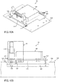
- FIG. 10A and FIG. 10B illustrate a certain reference example. Note that this reference example is not a prior art.
- a gate driver 10 of the reference example does not include the insulating member 120 used in this embodiment. Accordingly, a peripheral edge of a driver board 104 is open, and it is seen that a gap between the driver boards 102, 104 is not partitioned, either.
- Such a gate driver 10 of the reference example does not satisfy the standard (standard requirement) as an actual product because the driver board 104 including an input-side circuit PI is close to the other driver board 102 without a spatial distance satisfying the standard level therebetween and an insulation distance Id2 is not enough.
- an insulation distance Id3 between the input-side circuit PI and connection terminals 132 is not enough, either.
- the driver board 104 needs to be moved so as to be disposed at a height apart from the other driver board 102 by the spatial distance satisfying the standard requirement, leading to an increase in the mounting height (volume) of the whole gate driver 10.
- the gate driver 100 of this embodiment is far superior in that the whole size can be reduced with the mounting height reduced to the minimum owing to the sufficient insulation distances Id2, Id3.
- the gate driver 100 of this embodiment brings about the following advantages.
- FIG. 11 illustrates an example in which a gate driver 200 of another embodiment is used.
- the gate driver 200 of the other embodiment is different from the gate driver 100 of the above embodiment in that the shape of the periphery of one driver board 204 is different from that of the driver board 104 and accordingly the shape of an insulating member 220 is also different.
- the driver board 204 has a deformed H shape in a plan view, and output connectors 108 are arranged in the same direction as a coupling direction (lateral direction) of IGBT modules 130, 131. Further, regarding relay substrates 150 mounted on the IGBT modules 131 provided on both sides one per side, relay connectors 107, 109 are also arranged in the same direction as the coupling direction of the IGBT modules 130, 131. Note that other IGBT modules 133 may be coupled as in FIG. 8 , though the IGBT modules 133 are not illustrated in FIG. 11 .
- the example in which such a gate driver 200 of the other embodiment is used additionally has an advantage that it is possible to minimize the length of relay wiring lines 154 between the coupled IGBT modules 130, 131 to further reduce the weight and material cost. This effect is larger as the number of the coupled IGBT modules 130, 131 (133) is larger.
- the description is given using the example in which the gate driver 100 (200) has the two driver boards 102, 104 (202, 204), but the number of the driver boards may be three or more, and in this case, the division wall 126 can be disposed in each of the gaps (two places or more) between the facing circuit surfaces of the driver boards, and the plurality of division walls 126 may be integrally formed as the insulating member 120. Further, a structure with only one driver board may be adopted, and in this case, the peripheral edge of the single driver board is surrounded with the insulating member 120, and the division wall covering its lower surface need not be provided.
- the insulating member 120 is not limited to one including the flat surface walls 122, the bent walls 124, and the division wall 126 but may be constituted by an annular peripheral wall and a disk-shaped division wall, for instance. Further, the thickness, material, shape of each portion of the insulating member 120 are not limited to those exemplified in the embodiment, and the insulating member 120 can be variously modified as long as it enables to reduce the spatial distance and keep the necessary insulation distance.
- the output connectors 108 may be disposed, for example, at positions further lower than the position in the other embodiment in FIG. 11 to be disposed on both sides of the input connector 110.
- the driver board 104 and the insulating member 120 each can have a T-shape in a plan view.
- the output connectors 108 are mounted on both edge portions of the driver board 102, but instead, the two may be serially mounted on one edge portion of the driver board 102 or only one is mounted on one edge portion thereof.
- the driver board 104 may have a rectangular shape in a plan view.
- FIG. 8 and FIG. 11 show the form in which the other IGBT modules 131, 133, and so on are coupled to both sides of the IGBT module 130, but a form in which they are coupled only to one side may be adopted. Further, the number of the other coupled IGBT modules 131, 133 is not limited to the illustrated number, and in the case where they are coupled to both sides, their number may be different between both sides.
Landscapes
- Engineering & Computer Science (AREA)
- Microelectronics & Electronic Packaging (AREA)
- Power Engineering (AREA)
- Power Conversion In General (AREA)
- Inverter Devices (AREA)
Abstract
Description
- The present invention relates to a driver circuit device which drives an external device including a semiconductor element.
- A driver circuit device is typically used for driving a module having a power semiconductor such as IGBT (Insulated Gate-Bipolar Transistor), for instance. The publication issued by the Japan Patent Office (
JP5477157B2 - The power semiconductor module of the prior art example has the following structure. Specifically, semiconductor chips and wiring patterns are mounted on an insulating substrate, and conductors including the wiring patterns are electrically insulated from one another by ceramic layers or insulating layers, and the whole module is packaged with a case to be also insulated from an external part.
- On a package surface of the power semiconductor module, conductors such as external terminals for gate driving and main circuit terminals corresponding to collectors/emitters are greatly exposed. Therefore, the module terminals which are output-side elements when seen in terms of the relation with a gate driver or the like used in combination with the power semiconductor module need to be surely insulated also from input-side elements of the gate driver.
- It is an object of the present invention to provide a driver circuit device that can be surely insulated from an external device.
- To attain the aforesaid object, the present invention adopts the following configuration. Note that the parenthesized notes in the following description are only for reference and do not limit the present invention.
- A driver circuit device of a first configuration is usable with its circuit board being mounted on a driving-target external device, and the driver circuit device applies, to the external device, a drive signal generated in a driver circuit formed on the circuit board. The external device performs the switching of a relatively large current (power generation current, for instance) by using a power semiconductor element such as IGBT, for instance, and when seen in terms of the relation with the driver circuit device, the whole external device is an output side and part of the driver circuit device is an input side. Therefore, the input-side part of the driver circuit device needs to be surely insulated from the external device which is the output side.
- To achieve the insulation, the input-side element and the output-side element are disposed with a sufficient physical spatial distance (= insulation distance) therebetween. However, reserving a necessary space necessitates mounting the circuit board apart from the external device by the corresponding distance or disposing the terminals of the external device at positions apart from a mounting region of the circuit board, leading to an increase in the whole size including the mounting area and the mounting height.
- The driver circuit device of the first configuration has an insulating surrounding member that surrounds a peripheral edge of the circuit board, thereby having a sufficient insulation distance from the external device while a physical spatial distance that should be provided between the driver circuit device and the external device is reduced. Consequently, even in the state where the external device and the driver circuit device are combined, it is possible to reduce the whole size, enabling a space-saving and high-density arrangement.
- A driver circuit device of a second configuration includes a plurality of circuit boards. The plurality of circuit boards can be mounted on a driving-target external device with their circuit surfaces facing each other. By having the plurality of circuit boards where to form driver circuits, the driver circuit device can be further reduced in its whole mounting area. The driver circuit device applies, to an external device, drive signals generated in the driver circuits formed on the plurality of circuit boards. If an input-side circuit is formed on a specific circuit board out of the plurality of circuit boards, the other circuit board is an output side similarly to the external device, and accordingly, the insulation is also necessary between these circuit boards. For this purpose, in the second configuration, a space is kept between their circuit surfaces to insulate the input-side circuit and the output side from each other, and as for the circuit board on which the input-side circuit is formed, the insulating surrounding member is disposed to surround the peripheral edge of this circuit board. Consequently, a physical spatial distance that should be provided between the driver circuit device and the external device can be reduced yet a sufficient insulation distance can be kept therebetween. Further, even in the state where the external device and the driver circuit device are combined, it is also possible to reduce the whole size, enabling a space-saving and high-density arrangement.
- In the second configuration, a partition member can be further disposed between the plurality of circuit boards. In this case, even if the circuit surface of the circuit board on which the input-side circuit is formed and the circuit surface of the other circuit board face each other, a physical spatial distance that should be provided therebetween can be reduced, enabling a further reduction in the mounting height (dimension in a stacking direction of the circuit boards) of the driver circuit device.
- Further, the surrounding member and the partition member which are used in the second configuration can be integrated, and in this case, the structure is simplified and molding and assembling are facilitated.
- In the drawings used in the description of embodiments,
-
FIG. 1A and FIG. IB are respectively a perspective view and a plan view illustrating the configuration of a gate driver of one embodiment, -
FIG. 2 is an exploded perspective view of the gate driver, -
FIG. 3 is an exploded perspective view of the gate driver, -
FIG. 4 is a separation perspective view illustrating a mounting example of the gate driver, -
FIG. 5 is a circuit diagram illustrating the connection relation between the gate driver and an IGBT module, -
FIG. 6 is a vertical sectional view (sectional view along the V-V line inFIG. 1B ) of the gate driver, -
FIG. 7 is a plan view illustrating a state where the gate driver is mounted on the IGBT module, -
FIG. 8 is a plan view illustrating a coupling state of a plurality of IGBT modules, -
FIG. 9 is a diagram illustrating a circuit configuration in which the plurality of IGBT modules are coupled, -
FIG. 10A and FIG. 10B are respectively a perspective view and a side view illustrating the configuration of a gate driver of a reference example, and -
FIG. 11 is a plan view illustrating an example in which a gate driver of another embodiment is used. - Embodiments of a driver circuit device will be hereinafter described with reference to the drawings. In the following embodiments, though a gate driver is taken as an example of the driver circuit device and an IGBT module is taken as an example of a driving-target external device, the external device and the gate driver of the embodiments are not limited to these examples, and the external device may be a different power semiconductor module and the gate driver may be in a packaged state.
-
FIG. 1A is a perspective view illustrating the configuration of agate driver 100 of one embodiment, and FIG. IB is a plan view thereof. Further,FIG. 2 andFIG. 3 are exploded perspective views of thegate driver 100. - The
gate driver 100 includes twodriver boards FIG. 2 andFIG. 3 ). A not-illustrated gate driver circuit is formed on thedriver boards driver boards driver boards driver boards - On the driver board 104 (disposed on the upper side in
FIG. 1A to FIG. 3 ), a DC-DC converter 106, aninput connector 110, and various kinds of not-illustrated chip components are mounted, and besides, not-illustrated wiring patterns are formed. Wiring lines connecting to an external DC power source, a control unit, and so on, which are not illustrated, can be connected to theinput connector 110. The DC-DC converter 106 converts an externally input DC power (for example, DC +12 V) into a drive current for the gate driver circuit. Note that the external power source may be an AC power source, and in this case, an AC-DC converter or the like can be mounted on thedriver board 104. - The two
driver boards support pins 114 therebetween, and out of these, arrays of the lead pins 112 electrically connect thedriver boards driver boards driver boards - The not-illustrated gate driver circuit is formed on the two
driver boards - The
gate driver 100 further includes an insulatingmember 120 surrounding thedriver board 104. The insulatingmember 120 is formed of, for example, an insulating resin, and its whole shape is like that of a casing covering a lower surface of thedriver board 104 while surrounding a peripheral edge of thedriver board 104. - In more detail, in the
driver board 104, edge portions making a pair in one direction (X-axis direction inFIG. 2 andFIG. 3 ) are linear and edge portions making a pair in the other direction (Y-axis direction inFIG. 2 andFIG. 3 ) are cranked (bent). Accordingly, the insulatingmember 120 includes a pair offlat surface walls 122 and a pair ofbent walls 124 each having a shape along the corresponding edge portion of thedriver board 104. Such an insulatingmember 120 is disposed in a state of standing on the circuit surface of theother driver board 102. - The insulating
member 120 further includes a flat plate-shapeddivision wall 126 in its region covering the lower surface of thedriver board 104, and a peripheral edge of thedivision wall 126 is coupled with inner wall surfaces of theflat surface walls 122 and thebent walls 124. Further, thedivision wall 126 hasopenings openings FIG. 2 andFIG. 3 , of thedivision wall 126 is at a position slightly higher than lower ends of theflat surface walls 122 and thebent walls 124, ensuring that thedivision wall 126 and an upper circuit surface of theother driver board 102 are spaced. - On the other driver board 102 (disposed on the lower side in
FIG. 1A and FIG. 1B ), a pair ofoutput connectors 108 is mounted and besides, not-illustrated various chip components are mounted. On the circuit surface, theoutput connectors 108 are disposed at positions outside the insulatingmember 120, that is, are separated from thedriver board 104 by the insulatingmember 120. Because the edge portions of thedriver board 104 and thebent walls 124 are cranked, mounting ranges of theoutput connectors 108 and an installation range of the insulatingmember 120 do not interfere with each other on the circuit surface. The use purpose of theoutput connectors 108 will be further described later. - The
gate driver 100 is capable of driving semiconductor elements (IGBT) in the state of being mounted on the driving-target IGBT module 130 as illustrated inFIG. 4 . TheIGBT module 130 is provided with various kinds ofconnection terminals gate driver 100 is mounted thereon with lower surface terminals (not illustrated) of thedriver board 102 press-joined to theconnection terminals 136, for instance. Further, main conductors (+ and -) such as busbars are connected to theconnection terminals 132 which are located on one side of theIGBT module 130 in terms of the longitudinal detection and conductors for midpoint between the semiconductor elements are connected to theconnection terminals 134 which are located on the other side. - On the
IGBT module 130, a mounting region of thegate driver 100 is reserved in advance, and this mounting region is defined by a dimension L and a dimension W in the longitudinal direction and the width direction of theIGBT module 130 respectively, for instance. Accordingly, thegate driver 100 is structured such that the outside dimension of thedriver board 102 falls within the mounting region (dimensions L, W). -
FIG. 5 is a circuit diagram illustrating the connection relation between thegate driver 100 and theIGBT module 130. When mounted on theIGBT module 130 in the above-described manner, thegate driver 100 is electrically connected with theIGBT module 130 through theconnection terminals 136. - The
gate driver 100 includes twogate driver circuits IGBT module 130 respectively, and thegate driver circuits gate driver 100, thewhole IGBT module 130 can be considered as its driving-target external device or only a part corresponding to the semiconductor elements Q1, Q2 can be considered as its driving-target external device. - As described above, control signals are externally input to the
gate driver circuits FIG. 5 ), and besides, a DC current is also externally input (supplied) to the DC-DC converter 106. The drive current is supplied to thegate driver circuits DC converter 106. - At this time, in the
gate driver 100, an input-side (primary-side) circuit and an output-side (secondary-side) circuit are electrically insulated, and this input-side circuit PI includes theinput connector 110, a not-illustrated primary-side circuit in the DC-DC converter 106, not-illustrated primary-side circuits in thegate driver circuits - If the above part is defined as the input-side circuit PI, the
whole IGBT module 130 is an output-side circuit PO when seen in the state where thegate driver 100 is mounted thereon, and the output-side circuit PO at this time includes a not-illustrated secondary-side circuit in the DC-DC converter 106, not illustrated secondary-side circuits in thegate driver circuits - Therefore, an appropriate insulation distance Id needs to be kept between the input-side circuit PI and the output-side circuit PO, but there are various structural restrictions in keeping the insulation distance Id because the
gate driver 100 is structured to be mounted on the package surface of theIGBT module 130 as described above and thegate driver 100 itself needs to be as compact as possible to be reduced in its mounting height and mounting area. - The aforesaid structural restrictions would oblige a person with an ordinary skill in the art to provide a large spatial distance between the
gate driver 100 and theIGBT module 130 or make the mounting height of thegate driver 100 itself large to thereby keep the insulation distance Id. On the other hand, the inventors have succeeded in reducing a physical spatial distance between the input-side circuit PI and the output-side circuit PO by suitably disposing the insulatingmember 120. How the insulation distance Id is kept (the spatial distance is reduced) in the mounted state will be described below. - From here,
FIG. 6 andFIG. 7 will be referred to. InFIG. 6 , theIGBT module 130 which is a mounting destination is indicated by the two-dot chain line. - As described above, the input-side circuit PI includes the
input connector 110, the primary-side circuit of the DC-DC converter 106, the primary-side circuits in thegate driver circuits 141, 142 (not illustrated inFIG. 5 andFIG. 6 ), and so on, and they are structurally disposed in the range indicated by the bold broken line inFIG. 6 andFIG. 7 . Note that an insulatingelement 135 is mounted on thedriver board 104, and the dimension (standard dimension) of the insulatingelement 135 itself provides an insulation distance Id1 (requirement according to the standard: about 14 mm) in thedriver board 104. - In the
gate driver 100 as well, since a region outside the range of the input-side circuit PI is included in the output-side circuit PO, thelower driver board 102 has to be disposed with a sufficient insulation distance from the input-side circuit PI. If it is attempted to have this insulation distance by providing a physical spatial distance, the distance needs to be about equal to the insulation distance Id1 indicated inFIG. 5 , necessitating disposing the twodriver boards driver boards whole gate driver 100. - Therefore, in this embodiment, the insulating
division wall 126 partitions the gap (space) between the twodriver boards division wall 126 between the input-side circuit PI and the circuit surface of thedriver board 102 improves insulation performance, accordingly allowing a reduction in the physical spatial distance therebetween. This can make the mounting height of thewhole gate driver 100 low to contribute to downsizing. - As for the relation between the
gate driver 100 and theIGBT module 130, considering that theconnection terminals 132 are at positions near the input-side circuit PI when thegate driver 100 is in the mounted state and also considering that the busbars are connected to theconnection terminals 132, the input-side circuit PI and the connection terminals 132 (busbars in the connected state) should have an appropriate spatial distance therebetween. In this case, if it is attempted to mount thegate driver 100 within the predetermined mounting region, thedriver board 104 has to be disposed more apart in the height direction than in the illustrate state. However, disposing thedriver board 104 at such a height also causes the problem of extremely increasing the mounting height of thewhole gate driver 100. Note that it is difficult to dispose the input-side circuit PI closer to the middle of thedriver board 104 because of the limited board area, but disposing the input-side circuit PI on the opposite side causes another problem that its insulation distance cannot be kept from theother connection terminals 134. - Therefore, in this embodiment, the insulating
member 120 is disposed around the peripheral edge of thedriver board 104 on which the input-side circuit PI is mounted, to surround thedriver board 104 by theflat surface walls 122 and thebent walls 124, thereby keeping a sufficient insulation distance Id3 between the input-side circuit PI and the output-side circuit PO in theIGBT module 130 while making the physical spatial distance therebetween small (smaller than the insulation distance Id1). - That is, in the example in
FIG. 6 , the presence of theflat surface wall 122 between the input-side circuit PI and the connection terminals 132 (or the busbars in the connected state) of theIGBT module 130 improves insulation performance, accordingly allowing to dispose them close to each other with a reduced physical spatial distance. This can make the mounting height of thewhole gate driver 100 low to contribute to downsizing. - Further, in the example in
FIG. 7 , the periphery (three directions) of the input-side circuit PI is surrounded by theflat surface wall 122 and thebent walls 124. This allows theoutput connectors 108 to be disposed near the input-side circuit PI, making it possible to effectively use the limited mounting area on thedriver board 102 to increase the packaging density. - The
gate driver 100 of this embodiment is capable of not only driving the semiconductor elements by outputting (applying) the drive signals to theIGBT module 130 which is its mounting destination, but also driving the plurality ofIGBT modules other IGBT modules -
FIG. 8 illustrates a coupling state of the plurality ofIGBT modules - First, the coupling relation between the
IGBT module 130 and the other twoIGBT modules 131 will be described. The twoIGBT modules 131 are disposed on both sides one per side, across theIGBT module 130 on which thegate driver 100 is mounted. Further, arelay substrate 150 is mounted on each of theIGBT modules 131, and on each of therelay substrates 150,relay connectors relay connectors relay substrates 150 each have a circuit (not illustrated) that applies the drive signals which are input through the relay terminals, to theIGBT module 131 on which it is mounted. - On the
output connectors 108 of thegate driver 100, external output terminals (parallel drive terminals) capable of externally outputting the drive signals from thegate driver circuits output connectors 108 and therelay connectors 107 of therelay substrates 150 byrelay wiring lines 152 establishes the connection relation between thegate driver 100 and therelay substrates 150. In this manner, theIGBT module 130 is coupled with theIGBT modules 131 provided on both sides one per side. - Further, in this embodiment, still another
IGBT module 133 can be coupled, and in this case, theother IGBT module 133 can be coupled with each of theIGBT modules 131 coupled to both sides of theIGBT module 130 one per side. - That is, the other IGBT modules 133 (indicated by the two-dot chain lines in
FIG. 8 ) are disposed adjacently to theIGBT modules 131 provided on both sides one per side, whose connection relation is previously illustrated. At this time, on each of theother IGBT modules 133, thesame relay substrate 150 as that described above is mounted, and theIGBT modules 131 provided on both sides one per side can be connected to theIGBT modules 133 adjacent thereto by relay wiring lines 152. For the connection of therelay wiring lines 152, therelay connectors adjacent relay substrates 150 are used. For example, therelay wiring lines 152 extending from therelay connectors 109 of therelay substrates 150 mounted on theIGBT modules 131 provided on both sides one per side (theserelay wiring lines 152 are illustrated with part thereof being cut inFIG. 8 ) are connected to therelay connectors 107 of therelay substrates 150 mounted on theother IGBT modules 133 adjacent thereto. -
FIG. 9 illustrates a circuit configuration in which the plurality ofIGBT modules 130, 131 (133) are coupled. - As described above, the
IGBT modules 131 provided on both sides one per side are coupled across theIGBT module 130 on which thegate driver 100 of this embodiment is mounted. In this case, since theIGBT modules 131 have therelay substrates 150 mounted thereon, the drive signals output from thegate driver circuits gate driver 100 can be applied also to semiconductor elements Q1, Q2 of theIGBT modules 131 provided on both sides one per side. - Consequently, by externally outputting the drive signals to the relay terminals of the
relay connectors 107 through therelay wiring lines 152 from the external output terminals of theoutput connectors 108, thegate driver circuits gate driver 100 are capable of driving in parallel not only the semiconductor elements Q1, Q2 of themiddle IGBT module 130 but also the semiconductor elements Q1, Q2 of theIGBT modules 131 provided on both sides one per side, by using the drive signals. - Further, if the
other IGBT module 133 is disposed adjacently to each of theIGBT modules 131 provided on both sides one per side and the aforesaid connection therebetween is established by therelay wiring lines 152, the drive signals externally output from thegate driver circuits IGBT modules gate driver circuits middle IGBT module 130 and theIGBT modules 131 provided on both sides one per side but also semiconductor elements Q1, Q2 of theother IGBT modules 133 adjacent to theIGBT modules 131 respectively. It should be noted that the number of the coupledIGBT modules 133 is not limited to one and stillother IGBT modules 133 may be coupled in a row (any number of them can be coupled as long as the drive signals are kept at a level equal to or higher than a threshold value even in the attenuated state). - Further, in the state where the plurality of
IGBT modules 130, 131 (133) are coupled as illustrated inFIG. 9 , the other IGBT modules 131 (133) are included in the output-side circuit PO, and in this case as well, it is apparent that they have a sufficient insulation distance Id from the input-side circuit PI - Here, the applicability of this embodiment will be described using a reference example for comparison.
FIG. 10A and FIG. 10B illustrate a certain reference example. Note that this reference example is not a prior art. - A
gate driver 10 of the reference example does not include the insulatingmember 120 used in this embodiment. Accordingly, a peripheral edge of adriver board 104 is open, and it is seen that a gap between thedriver boards - Such a
gate driver 10 of the reference example does not satisfy the standard (standard requirement) as an actual product because thedriver board 104 including an input-side circuit PI is close to theother driver board 102 without a spatial distance satisfying the standard level therebetween and an insulation distance Id2 is not enough. Similarly, in terms of the relation with anIGBT module 130 on which it is mounted, an insulation distance Id3 between the input-side circuit PI andconnection terminals 132 is not enough, either. - Therefore, to increase the insulation distances Id2, Id3 to sufficient levels in the
gate driver 10 of the reference example, thedriver board 104 needs to be moved so as to be disposed at a height apart from theother driver board 102 by the spatial distance satisfying the standard requirement, leading to an increase in the mounting height (volume) of thewhole gate driver 10. - In this respect, the
gate driver 100 of this embodiment is far superior in that the whole size can be reduced with the mounting height reduced to the minimum owing to the sufficient insulation distances Id2, Id3. - The
gate driver 100 of this embodiment brings about the following advantages. - (1) It is possible to keep the sufficient insulation distances Id2, Id3 between the input-side circuit PI and the output-side circuit PO, yet shorten the physical spatial distance therebetween to reduce the mounting height (volume).
- (2) Further, even in the case where the mounting region is prescribed on the
IGBT module 130 which is the driving target (mounting destination), it is possible to obtain the circuit configuration with sufficient performance by making the best use of the limited mounting region. - (3) The
gate driver 100 has such a size as not to protrude to the outside of theIGBT module 130 in a plan view. Accordingly, even when the plurality of modules are coupled as illustrated inFIG. 8 , it is possible to narrow an arrangement interval between theIGBT modules - (4) The insulating
member 120 is structured to have theflat surface walls 122, thebent walls 124, and thedivision wall 126 and they each have a unique insulation function, but since they are all integrally formed, it is possible to achieve easiness at the time of the manufacture and assembly, reduce production cost, and improve production efficiency. - (5) Further, the insulating
member 120 is disposed only at a place where the insulation distance is necessary and does not package the whole including thedriver board 104 and its mounted components, enabling a reduction in the number of used materials and weight, a reduction in production cost, and an increase in production efficiency. - (6) Since the insulating
member 120 and thedriver board 104 do not interfere with the mounting ranges of theoutput connectors 108 which are used when the plurality ofIGBT modules -
FIG. 11 illustrates an example in which agate driver 200 of another embodiment is used. Thegate driver 200 of the other embodiment is different from thegate driver 100 of the above embodiment in that the shape of the periphery of onedriver board 204 is different from that of thedriver board 104 and accordingly the shape of an insulatingmember 220 is also different. - Specifically, the
driver board 204 has a deformed H shape in a plan view, andoutput connectors 108 are arranged in the same direction as a coupling direction (lateral direction) ofIGBT modules relay substrates 150 mounted on theIGBT modules 131 provided on both sides one per side,relay connectors IGBT modules other IGBT modules 133 may be coupled as inFIG. 8 , though theIGBT modules 133 are not illustrated inFIG. 11 . - The example in which such a
gate driver 200 of the other embodiment is used additionally has an advantage that it is possible to minimize the length ofrelay wiring lines 154 between the coupledIGBT modules IGBT modules 130, 131 (133) is larger. - Further, in the embodiments, the description is given using the example in which the gate driver 100 (200) has the two
driver boards 102, 104 (202, 204), but the number of the driver boards may be three or more, and in this case, thedivision wall 126 can be disposed in each of the gaps (two places or more) between the facing circuit surfaces of the driver boards, and the plurality ofdivision walls 126 may be integrally formed as the insulatingmember 120. Further, a structure with only one driver board may be adopted, and in this case, the peripheral edge of the single driver board is surrounded with the insulatingmember 120, and the division wall covering its lower surface need not be provided. - The insulating
member 120 is not limited to one including theflat surface walls 122, thebent walls 124, and thedivision wall 126 but may be constituted by an annular peripheral wall and a disk-shaped division wall, for instance. Further, the thickness, material, shape of each portion of the insulatingmember 120 are not limited to those exemplified in the embodiment, and the insulatingmember 120 can be variously modified as long as it enables to reduce the spatial distance and keep the necessary insulation distance. - The
output connectors 108 may be disposed, for example, at positions further lower than the position in the other embodiment inFIG. 11 to be disposed on both sides of theinput connector 110. In this case, thedriver board 104 and the insulatingmember 120 each can have a T-shape in a plan view. - Further, in the plan view of
FIG. 8 , theoutput connectors 108 are mounted on both edge portions of thedriver board 102, but instead, the two may be serially mounted on one edge portion of thedriver board 102 or only one is mounted on one edge portion thereof. Further, thedriver board 104 may have a rectangular shape in a plan view. - The examples in
FIG. 8 andFIG. 11 show the form in which theother IGBT modules IGBT module 130, but a form in which they are coupled only to one side may be adopted. Further, the number of the other coupledIGBT modules - Besides, the structures described with the illustration in the embodiments and the application examples are only suitable examples, and various elements may be added to the basic structures or the basic structures may be partly replaced.
Claims (6)
- A driver circuit device (100) which drives a semiconductor element (Q1, Q2) that a driving-target external device (130) has,
characterized in that the driver circuit device (100) comprises:a circuit board (102, 104) mountable on the driving-target external device (130);a driver circuit (141, 142) which is formed on the circuit board (102, 104) and applies, to the external device (130), a drive signal generated using power and a signal which are externally input, andan insulating surrounding member (122, 124) disposed to surround a peripheral edge of the circuit board (102, 104). - The driver circuit device (100) according to claim 1, characterized in that:the circuit board (102, 104) includes a plurality of circuit boards (102, 104) mountable on the driving-target external device (130) while a space is kept between facing circuit surfaces of the plurality of circuit boards (102, 104);the driver circuit (141, 142) is formed on one of the plurality of circuit boards (102, 104); andthe driver circuit device (100) further includes an insulating surrounding member (122, 124) disposed to surround a peripheral edge of the circuit board (104) on which a circuit on an input side to the driver circuit (141, 142) is formed, out of the plurality of circuit boards (102, 104).
- The driver circuit device (100) according to claim 2,
characterized in that the driver circuit device (100) further comprises
an insulating partition member (126) disposed in the space to partition a gap between the circuit surfaces. - The driver circuit device (100) according to claim 3,
characterized in that the surrounding member (122, 124) and the partition member (126) are integrated, with a peripheral edge of the partition member (126) coupled with the surrounding member (122, 124). - The driver circuit device (100) according to any one of claims 1 to 4,
characterized in that:the driver circuit device (100) further comprises a parallel drive terminal (108) which is disposed on the circuit board (102, 104) and is capable of externally outputting the drive signal in parallel to another external device (131) disposed in addition to the external device (130) on which the driver circuit device (100) is mounted; andin a state where a relay substrate (150) having a circuit which applies, to the other external device (131), the drive signal input through a predetermined relay terminal (107) is mounted on the other external device (131), the driver circuit (141,142) is capable of driving the other external device (131) in parallel by using the drive signal that the driver circuit (141, 142) externally outputs from the parallel drive terminal (108) to the relay terminal (107) through a wiring line. - The driver circuit device (100) according to claim 5,
characterized in that:another relay terminal (109) is disposed on the relay substrate (150), the other relay terminal (109) capable of externally outputting the drive signal to still another external device (133) in parallel while applying the drive signal to the other external device (131) on which the relay substrate (150) is mounted; andin a state where the relay substrate (150) is mounted on each of a first external device (131) and a second external device (133) which are the other external devices, the parallel drive terminal (108) is connected, by a wiring line, to the relay terminal (109) of the relay substrate (150) mounted on the first external device (131), and the relay terminals (109, 107) of the first external device (131) and the second external device (133) are connected to each other by a wiring line,the driver circuit (141, 142) is capable of driving the first external device (131) and the second external device (133) in parallel by using the drive signal which is externally output from the parallel drive terminal (108).
Applications Claiming Priority (1)
| Application Number | Priority Date | Filing Date | Title |
|---|---|---|---|
| JP2019047696A JP6915890B2 (en) | 2019-03-14 | 2019-03-14 | Drive circuit device |
Publications (3)
| Publication Number | Publication Date |
|---|---|
| EP3709781A1 true EP3709781A1 (en) | 2020-09-16 |
| EP3709781B1 EP3709781B1 (en) | 2024-05-01 |
| EP3709781C0 EP3709781C0 (en) | 2024-05-01 |
Family
ID=69784077
Family Applications (1)
| Application Number | Title | Priority Date | Filing Date |
|---|---|---|---|
| EP20161175.3A Active EP3709781B1 (en) | 2019-03-14 | 2020-03-05 | Driver circuit device |
Country Status (5)
| Country | Link |
|---|---|
| US (1) | US11503725B2 (en) |
| EP (1) | EP3709781B1 (en) |
| JP (1) | JP6915890B2 (en) |
| CN (2) | CN111697796B (en) |
| ES (1) | ES2982471T3 (en) |
Families Citing this family (5)
| Publication number | Priority date | Publication date | Assignee | Title |
|---|---|---|---|---|
| JP6915890B2 (en) * | 2019-03-14 | 2021-08-04 | 株式会社タムラ製作所 | Drive circuit device |
| JP1782542S (en) * | 2023-04-20 | 2024-10-17 | Semiconductor driver circuit module | |
| JP1753053S (en) * | 2023-04-20 | 2023-09-13 | Semiconductor drive circuit module | |
| JP7711125B2 (en) * | 2023-05-08 | 2025-07-22 | 株式会社タムラ製作所 | Drive circuit device |
| TWI872853B (en) | 2023-12-07 | 2025-02-11 | 朋程科技股份有限公司 | Drive device |
Citations (3)
| Publication number | Priority date | Publication date | Assignee | Title |
|---|---|---|---|---|
| US20090002956A1 (en) * | 2007-06-22 | 2009-01-01 | Hitachi, Ltd. | Power Converter |
| JP5477157B2 (en) | 2010-05-17 | 2014-04-23 | 富士電機株式会社 | Semiconductor device |
| US20160079744A1 (en) * | 2014-09-11 | 2016-03-17 | Keihin Corporation | Power conversion apparatus |
Family Cites Families (13)
| Publication number | Priority date | Publication date | Assignee | Title |
|---|---|---|---|---|
| JPS5587699A (en) | 1978-12-25 | 1980-07-02 | Mitsubishi Heavy Ind Ltd | Propulsion system for propeller ship |
| JPH1098887A (en) * | 1996-09-20 | 1998-04-14 | Hitachi Ltd | Power converter |
| JP4163360B2 (en) * | 2000-02-21 | 2008-10-08 | 三菱電機株式会社 | Power module |
| US8007255B2 (en) * | 2006-11-22 | 2011-08-30 | Mitsubishi Heavy Industries, Ltd. | Inverter-integrated electric compressor with inverter storage box arrangement |
| JP4452952B2 (en) * | 2007-06-20 | 2010-04-21 | 日立オートモティブシステムズ株式会社 | Power converter |
| CN104011988A (en) * | 2012-02-07 | 2014-08-27 | 富士电机株式会社 | Electric power conversion device |
| US9935526B2 (en) * | 2012-04-16 | 2018-04-03 | Mitsubishi Electric Corporation | Electric rotating machine |
| JP6045992B2 (en) * | 2013-07-04 | 2016-12-14 | 本田技研工業株式会社 | Power switching equipment |
| JP6227150B2 (en) | 2014-08-29 | 2017-11-08 | 三菱電機株式会社 | Semiconductor device and multiphase semiconductor device |
| JP6170640B1 (en) | 2017-03-15 | 2017-07-26 | イサハヤ電子株式会社 | Gate drive board with parallel connector |
| JP6130959B1 (en) | 2016-07-19 | 2017-05-17 | イサハヤ電子株式会社 | Connector-connected gate parallel connection board |
| CN107852085B (en) * | 2016-07-19 | 2020-01-03 | 谏早电子株式会社 | Connector-connected gate parallel connection substrate and gate drive substrate |
| JP6915890B2 (en) * | 2019-03-14 | 2021-08-04 | 株式会社タムラ製作所 | Drive circuit device |
-
2019
- 2019-03-14 JP JP2019047696A patent/JP6915890B2/en active Active
-
2020
- 2020-02-06 CN CN202010081544.0A patent/CN111697796B/en active Active
- 2020-02-06 CN CN202020154656.XU patent/CN211959061U/en active Active
- 2020-03-05 EP EP20161175.3A patent/EP3709781B1/en active Active
- 2020-03-05 ES ES20161175T patent/ES2982471T3/en active Active
- 2020-03-12 US US16/816,791 patent/US11503725B2/en active Active
Patent Citations (3)
| Publication number | Priority date | Publication date | Assignee | Title |
|---|---|---|---|---|
| US20090002956A1 (en) * | 2007-06-22 | 2009-01-01 | Hitachi, Ltd. | Power Converter |
| JP5477157B2 (en) | 2010-05-17 | 2014-04-23 | 富士電機株式会社 | Semiconductor device |
| US20160079744A1 (en) * | 2014-09-11 | 2016-03-17 | Keihin Corporation | Power conversion apparatus |
Also Published As
| Publication number | Publication date |
|---|---|
| US20200296845A1 (en) | 2020-09-17 |
| CN111697796A (en) | 2020-09-22 |
| EP3709781B1 (en) | 2024-05-01 |
| US11503725B2 (en) | 2022-11-15 |
| ES2982471T3 (en) | 2024-10-16 |
| CN211959061U (en) | 2020-11-17 |
| JP6915890B2 (en) | 2021-08-04 |
| EP3709781C0 (en) | 2024-05-01 |
| CN111697796B (en) | 2025-11-04 |
| JP2020150178A (en) | 2020-09-17 |
Similar Documents
| Publication | Publication Date | Title |
|---|---|---|
| EP3709781B1 (en) | Driver circuit device | |
| CN102237326B (en) | Semiconductor device | |
| US10159166B2 (en) | Heat dissipating structure | |
| CN113013126A (en) | Half-bridge module of a traction inverter of a power electronics system of a vehicle | |
| US11570921B2 (en) | Semiconductor device with stacked terminals | |
| US7541670B2 (en) | Semiconductor device having terminals | |
| WO2017130421A1 (en) | Semiconductor module | |
| CN111033996A (en) | Busbar and power module | |
| JP3941266B2 (en) | Semiconductor power module | |
| JP2023180525A (en) | power converter | |
| US10251256B2 (en) | Heat dissipating structure | |
| KR100843734B1 (en) | Semiconductor power module and manufacturing method | |
| TW202332357A (en) | Power module | |
| CN111834353B (en) | SIP laminated structure | |
| WO2021180660A1 (en) | Power module | |
| US6788546B1 (en) | Multi-chip module | |
| US20220181316A1 (en) | Electronic chips with surface mount component | |
| JP4695918B2 (en) | Power module | |
| JP4580270B2 (en) | Power module | |
| US11373804B2 (en) | Capacitor structure and power module having a power electronic component | |
| KR100894796B1 (en) | Multi-layered Power Semiconductor Module | |
| JP7533740B2 (en) | Power Conversion Equipment | |
| KR102432054B1 (en) | Power conditioning system | |
| JP7711125B2 (en) | Drive circuit device | |
| CN121035064A (en) | Power modules and electronic devices |
Legal Events
| Date | Code | Title | Description |
|---|---|---|---|
| PUAI | Public reference made under article 153(3) epc to a published international application that has entered the european phase |
Free format text: ORIGINAL CODE: 0009012 |
|
| STAA | Information on the status of an ep patent application or granted ep patent |
Free format text: STATUS: THE APPLICATION HAS BEEN PUBLISHED |
|
| AK | Designated contracting states |
Kind code of ref document: A1 Designated state(s): AL AT BE BG CH CY CZ DE DK EE ES FI FR GB GR HR HU IE IS IT LI LT LU LV MC MK MT NL NO PL PT RO RS SE SI SK SM TR |
|
| AX | Request for extension of the european patent |
Extension state: BA ME |
|
| RIC1 | Information provided on ipc code assigned before grant |
Ipc: H05K 7/14 20060101AFI20201117BHEP Ipc: H05K 5/02 20060101ALI20201117BHEP |
|
| STAA | Information on the status of an ep patent application or granted ep patent |
Free format text: STATUS: REQUEST FOR EXAMINATION WAS MADE |
|
| 17P | Request for examination filed |
Effective date: 20210312 |
|
| RBV | Designated contracting states (corrected) |
Designated state(s): AL AT BE BG CH CY CZ DE DK EE ES FI FR GB GR HR HU IE IS IT LI LT LU LV MC MK MT NL NO PL PT RO RS SE SI SK SM TR |
|
| STAA | Information on the status of an ep patent application or granted ep patent |
Free format text: STATUS: EXAMINATION IS IN PROGRESS |
|
| 17Q | First examination report despatched |
Effective date: 20220707 |
|
| GRAP | Despatch of communication of intention to grant a patent |
Free format text: ORIGINAL CODE: EPIDOSNIGR1 |
|
| STAA | Information on the status of an ep patent application or granted ep patent |
Free format text: STATUS: GRANT OF PATENT IS INTENDED |
|
| INTG | Intention to grant announced |
Effective date: 20231017 |
|
| GRAS | Grant fee paid |
Free format text: ORIGINAL CODE: EPIDOSNIGR3 |
|
| GRAA | (expected) grant |
Free format text: ORIGINAL CODE: 0009210 |
|
| STAA | Information on the status of an ep patent application or granted ep patent |
Free format text: STATUS: THE PATENT HAS BEEN GRANTED |
|
| AK | Designated contracting states |
Kind code of ref document: B1 Designated state(s): AL AT BE BG CH CY CZ DE DK EE ES FI FR GB GR HR HU IE IS IT LI LT LU LV MC MK MT NL NO PL PT RO RS SE SI SK SM TR |
|
| REG | Reference to a national code |
Ref country code: GB Ref legal event code: FG4D |
|
| REG | Reference to a national code |
Ref country code: CH Ref legal event code: EP |
|
| REG | Reference to a national code |
Ref country code: IE Ref legal event code: FG4D |
|
| REG | Reference to a national code |
Ref country code: DE Ref legal event code: R096 Ref document number: 602020029887 Country of ref document: DE |
|
| U01 | Request for unitary effect filed |
Effective date: 20240501 |
|
| U07 | Unitary effect registered |
Designated state(s): AT BE BG DE DK EE FI FR IT LT LU LV MT NL PT SE SI Effective date: 20240510 |
|
| PG25 | Lapsed in a contracting state [announced via postgrant information from national office to epo] |
Ref country code: IS Free format text: LAPSE BECAUSE OF FAILURE TO SUBMIT A TRANSLATION OF THE DESCRIPTION OR TO PAY THE FEE WITHIN THE PRESCRIBED TIME-LIMIT Effective date: 20240901 |
|
| PG25 | Lapsed in a contracting state [announced via postgrant information from national office to epo] |
Ref country code: HR Free format text: LAPSE BECAUSE OF FAILURE TO SUBMIT A TRANSLATION OF THE DESCRIPTION OR TO PAY THE FEE WITHIN THE PRESCRIBED TIME-LIMIT Effective date: 20240501 |
|
| PG25 | Lapsed in a contracting state [announced via postgrant information from national office to epo] |
Ref country code: GR Free format text: LAPSE BECAUSE OF FAILURE TO SUBMIT A TRANSLATION OF THE DESCRIPTION OR TO PAY THE FEE WITHIN THE PRESCRIBED TIME-LIMIT Effective date: 20240802 |
|
| REG | Reference to a national code |
Ref country code: ES Ref legal event code: FG2A Ref document number: 2982471 Country of ref document: ES Kind code of ref document: T3 Effective date: 20241016 |
|
| PG25 | Lapsed in a contracting state [announced via postgrant information from national office to epo] |
Ref country code: PL Free format text: LAPSE BECAUSE OF FAILURE TO SUBMIT A TRANSLATION OF THE DESCRIPTION OR TO PAY THE FEE WITHIN THE PRESCRIBED TIME-LIMIT Effective date: 20240501 |
|
| PG25 | Lapsed in a contracting state [announced via postgrant information from national office to epo] |
Ref country code: PL Free format text: LAPSE BECAUSE OF FAILURE TO SUBMIT A TRANSLATION OF THE DESCRIPTION OR TO PAY THE FEE WITHIN THE PRESCRIBED TIME-LIMIT Effective date: 20240501 Ref country code: NO Free format text: LAPSE BECAUSE OF FAILURE TO SUBMIT A TRANSLATION OF THE DESCRIPTION OR TO PAY THE FEE WITHIN THE PRESCRIBED TIME-LIMIT Effective date: 20240801 Ref country code: IS Free format text: LAPSE BECAUSE OF FAILURE TO SUBMIT A TRANSLATION OF THE DESCRIPTION OR TO PAY THE FEE WITHIN THE PRESCRIBED TIME-LIMIT Effective date: 20240901 Ref country code: HR Free format text: LAPSE BECAUSE OF FAILURE TO SUBMIT A TRANSLATION OF THE DESCRIPTION OR TO PAY THE FEE WITHIN THE PRESCRIBED TIME-LIMIT Effective date: 20240501 Ref country code: GR Free format text: LAPSE BECAUSE OF FAILURE TO SUBMIT A TRANSLATION OF THE DESCRIPTION OR TO PAY THE FEE WITHIN THE PRESCRIBED TIME-LIMIT Effective date: 20240802 Ref country code: RS Free format text: LAPSE BECAUSE OF FAILURE TO SUBMIT A TRANSLATION OF THE DESCRIPTION OR TO PAY THE FEE WITHIN THE PRESCRIBED TIME-LIMIT Effective date: 20240801 |
|
| PG25 | Lapsed in a contracting state [announced via postgrant information from national office to epo] |
Ref country code: CZ Free format text: LAPSE BECAUSE OF FAILURE TO SUBMIT A TRANSLATION OF THE DESCRIPTION OR TO PAY THE FEE WITHIN THE PRESCRIBED TIME-LIMIT Effective date: 20240501 |
|
| PG25 | Lapsed in a contracting state [announced via postgrant information from national office to epo] |
Ref country code: SK Free format text: LAPSE BECAUSE OF FAILURE TO SUBMIT A TRANSLATION OF THE DESCRIPTION OR TO PAY THE FEE WITHIN THE PRESCRIBED TIME-LIMIT Effective date: 20240501 |
|
| PG25 | Lapsed in a contracting state [announced via postgrant information from national office to epo] |
Ref country code: SM Free format text: LAPSE BECAUSE OF FAILURE TO SUBMIT A TRANSLATION OF THE DESCRIPTION OR TO PAY THE FEE WITHIN THE PRESCRIBED TIME-LIMIT Effective date: 20240501 |
|
| PG25 | Lapsed in a contracting state [announced via postgrant information from national office to epo] |
Ref country code: SM Free format text: LAPSE BECAUSE OF FAILURE TO SUBMIT A TRANSLATION OF THE DESCRIPTION OR TO PAY THE FEE WITHIN THE PRESCRIBED TIME-LIMIT Effective date: 20240501 Ref country code: SK Free format text: LAPSE BECAUSE OF FAILURE TO SUBMIT A TRANSLATION OF THE DESCRIPTION OR TO PAY THE FEE WITHIN THE PRESCRIBED TIME-LIMIT Effective date: 20240501 Ref country code: CZ Free format text: LAPSE BECAUSE OF FAILURE TO SUBMIT A TRANSLATION OF THE DESCRIPTION OR TO PAY THE FEE WITHIN THE PRESCRIBED TIME-LIMIT Effective date: 20240501 |
|
| REG | Reference to a national code |
Ref country code: DE Ref legal event code: R097 Ref document number: 602020029887 Country of ref document: DE |
|
| PLBE | No opposition filed within time limit |
Free format text: ORIGINAL CODE: 0009261 |
|
| STAA | Information on the status of an ep patent application or granted ep patent |
Free format text: STATUS: NO OPPOSITION FILED WITHIN TIME LIMIT |
|
| 26N | No opposition filed |
Effective date: 20250204 |
|
| U20 | Renewal fee for the european patent with unitary effect paid |
Year of fee payment: 6 Effective date: 20250325 |
|
| PGFP | Annual fee paid to national office [announced via postgrant information from national office to epo] |
Ref country code: ES Payment date: 20250429 Year of fee payment: 6 |
|
| PGFP | Annual fee paid to national office [announced via postgrant information from national office to epo] |
Ref country code: CH Payment date: 20250401 Year of fee payment: 6 |
|
| PG25 | Lapsed in a contracting state [announced via postgrant information from national office to epo] |
Ref country code: MC Free format text: LAPSE BECAUSE OF FAILURE TO SUBMIT A TRANSLATION OF THE DESCRIPTION OR TO PAY THE FEE WITHIN THE PRESCRIBED TIME-LIMIT Effective date: 20240501 |
|
| GBPC | Gb: european patent ceased through non-payment of renewal fee |
Effective date: 20250305 |
|
| PG25 | Lapsed in a contracting state [announced via postgrant information from national office to epo] |
Ref country code: GB Free format text: LAPSE BECAUSE OF NON-PAYMENT OF DUE FEES Effective date: 20250305 |
|
| PG25 | Lapsed in a contracting state [announced via postgrant information from national office to epo] |
Ref country code: IE Free format text: LAPSE BECAUSE OF NON-PAYMENT OF DUE FEES Effective date: 20250305 |
|
| REG | Reference to a national code |
Ref country code: CH Ref legal event code: U11 Free format text: ST27 STATUS EVENT CODE: U-0-0-U10-U11 (AS PROVIDED BY THE NATIONAL OFFICE) Effective date: 20260401 |
|
| PGFP | Annual fee paid to national office [announced via postgrant information from national office to epo] |
Ref country code: RO Payment date: 20260225 Year of fee payment: 7 |
|
| U20 | Renewal fee for the european patent with unitary effect paid |
Year of fee payment: 7 Effective date: 20260326 |