EP3709518A1 - Delta-sigma modulator with truncation error compensation and associated method - Google Patents
Delta-sigma modulator with truncation error compensation and associated method Download PDFInfo
- Publication number
- EP3709518A1 EP3709518A1 EP20161567.1A EP20161567A EP3709518A1 EP 3709518 A1 EP3709518 A1 EP 3709518A1 EP 20161567 A EP20161567 A EP 20161567A EP 3709518 A1 EP3709518 A1 EP 3709518A1
- Authority
- EP
- European Patent Office
- Prior art keywords
- signal
- digital
- truncation error
- circuit
- analog
- Prior art date
- Legal status (The legal status is an assumption and is not a legal conclusion. Google has not performed a legal analysis and makes no representation as to the accuracy of the status listed.)
- Ceased
Links
- 238000000034 method Methods 0.000 title claims description 23
- 238000012546 transfer Methods 0.000 claims description 32
- 238000013139 quantization Methods 0.000 claims description 12
- 238000006243 chemical reaction Methods 0.000 claims description 8
- 238000001914 filtration Methods 0.000 claims description 5
- 238000010586 diagram Methods 0.000 description 14
- 238000007493 shaping process Methods 0.000 description 7
- 230000003111 delayed effect Effects 0.000 description 4
- 230000004044 response Effects 0.000 description 3
- 238000012545 processing Methods 0.000 description 2
- 230000004075 alteration Effects 0.000 description 1
- 230000008901 benefit Effects 0.000 description 1
- 238000013461 design Methods 0.000 description 1
- 238000002347 injection Methods 0.000 description 1
- 239000007924 injection Substances 0.000 description 1
- 238000012986 modification Methods 0.000 description 1
- 230000004048 modification Effects 0.000 description 1
- 230000008569 process Effects 0.000 description 1
- 230000009467 reduction Effects 0.000 description 1
- 238000005070 sampling Methods 0.000 description 1
Images



Classifications
-
- H—ELECTRICITY
- H03—ELECTRONIC CIRCUITRY
- H03M—CODING; DECODING; CODE CONVERSION IN GENERAL
- H03M3/00—Conversion of analogue values to or from differential modulation
- H03M3/30—Delta-sigma modulation
- H03M3/322—Continuously compensating for, or preventing, undesired influence of physical parameters
- H03M3/368—Continuously compensating for, or preventing, undesired influence of physical parameters of noise other than the quantisation noise already being shaped inherently by delta-sigma modulators
-
- H—ELECTRICITY
- H03—ELECTRONIC CIRCUITRY
- H03M—CODING; DECODING; CODE CONVERSION IN GENERAL
- H03M3/00—Conversion of analogue values to or from differential modulation
- H03M3/30—Delta-sigma modulation
- H03M3/458—Analogue/digital converters using delta-sigma modulation as an intermediate step
- H03M3/464—Details of the digital/analogue conversion in the feedback path
-
- H—ELECTRICITY
- H03—ELECTRONIC CIRCUITRY
- H03M—CODING; DECODING; CODE CONVERSION IN GENERAL
- H03M3/00—Conversion of analogue values to or from differential modulation
- H03M3/30—Delta-sigma modulation
- H03M3/322—Continuously compensating for, or preventing, undesired influence of physical parameters
-
- H—ELECTRICITY
- H03—ELECTRONIC CIRCUITRY
- H03M—CODING; DECODING; CODE CONVERSION IN GENERAL
- H03M3/00—Conversion of analogue values to or from differential modulation
- H03M3/30—Delta-sigma modulation
- H03M3/39—Structural details of delta-sigma modulators, e.g. incremental delta-sigma modulators
- H03M3/412—Structural details of delta-sigma modulators, e.g. incremental delta-sigma modulators characterised by the number of quantisers and their type and resolution
- H03M3/422—Structural details of delta-sigma modulators, e.g. incremental delta-sigma modulators characterised by the number of quantisers and their type and resolution having one quantiser only
- H03M3/424—Structural details of delta-sigma modulators, e.g. incremental delta-sigma modulators characterised by the number of quantisers and their type and resolution having one quantiser only the quantiser being a multiple bit one
- H03M3/426—Structural details of delta-sigma modulators, e.g. incremental delta-sigma modulators characterised by the number of quantisers and their type and resolution having one quantiser only the quantiser being a multiple bit one the quantiser being a successive approximation type analogue/digital converter
Definitions
- the present invention relates to delta-sigma modulation, and more particularly, to a delta-sigma modulator with truncation error compensation and an associated method.
- a multi-level digital-to-analog converter In a conventional delta-sigma modulator with a multi-bit quantizer, a multi-level digital-to-analog converter (DAC) is required to feed back an output signal of the delta-sigma modulator and to work with a loop filter and a quantizer to implement a closed-loop system for noise-shaping function.
- DAC digital-to-analog converter
- a mismatch between the DAC cells contributes mismatch errors. Since the digital input to the feedback DAC determines the selection of DAC cells included in the feedback DAC, these mismatches result in non-linearity in the analog output of the feedback DAC.
- a dynamic element matching (DEM) function is a well-known strategy to address the mismatch issue of the multi-level feedback DAC, but the hardware complexity grows exponentially as a bit number of the feedback DAC increases. Thus, there is a need for an innovative feedback DAC reduction technique in a delta-sigma modulator.
- One of the objectives of the claimed invention is to provide a delta-sigma modulator with truncation error compensation and an associated method.
- an exemplary delta-sigma modulator includes a first combining circuit, a loop filter circuit, a quantizer circuit, a truncator circuit, a first digital-to-analog converter (DAC) circuit, and a compensation circuit.
- the first combining circuit is arranged to receive an analog input signal and an analog feedback signal, and generate a first analog signal by combining the analog feedback signal and the analog input signal.
- the loop filter circuit is arranged to receive the first analog signal, and generate a loop-filtered signal according to the first analog signal.
- the quantizer circuit is arranged to output a first digital signal that is indicative of a digital combination result of at least a truncation error compensation signal and the loop-filtered signal.
- the truncator circuit is arranged to perform truncation upon the first digital signal to generate a second digital signal, wherein a bit number of the second digital signal is smaller than a bit number of the first digital signal.
- the first DAC circuit is arranged to receive the second digital signal, and generate the analog feedback signal according to the second digital signal.
- the compensation circuit is arranged to generate the truncation error compensation signal according to a truncation error resulting from said truncation performed upon the first digital signal.
- an exemplary delta-sigma modulation method includes: generating a first analog signal by combining an analog feedback signal and an analog input signal; generating a loop-filtered signal by applying loop filtering to the first analog signal; performing quantization to output a first digital signal that is indicative of a digital combination result of at least a truncation error compensation signal and the loop-filtered signal; performing truncation upon the first digital signal to generate a second digital signal, wherein a bit number of the second digital signal is smaller than a bit number of the first digital signal; performing digital-to-analog conversion upon the second digital signal to generate the analog feedback signal; and generating the truncation error compensation signal according to a truncation error resulting from said truncation performed upon the first digital signal.
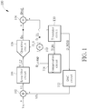
- FIG. 1 is a diagram illustrating a first delta-sigma modulator according to an embodiment of the present invention.
- the delta-sigma modulator 100 may be a part of a delta-sigma analog-to-digital converter (ADC).
- ADC analog-to-digital converter
- an analog input signal Vin of the delta-sigma modulator 100 may be an analog input of the delta-sigma ADC
- a digital output of the delta-sigma ADC may be generated by processing a digital output signal Dout of the delta-sigma modulator 100 through a digital filter and a decimation filter.
- ADC analog-to-digital converter
- the delta-sigma modulator 100 includes a plurality of combining circuits 102, 103, 104, a loop filter circuit 106, a quantizer circuit 108, a digital-to-analog converter (DAC) circuit 112, a truncator circuit 110, and a compensation circuit 114.
- the combining circuit 102 is arranged to receive the analog input signal Vin and an analog feedback signal Vfb, and generate an analog signal V1 by combining the analog feedback signal Vfb and the analog input signal Vin.
- the loop filter circuit is arranged to receive the analog signal V1, and generate a loop-filtered signal V_LF according to the analog signal V1.
- the quantizer circuit 108 is arranged to perform quantization to output a digital signal Do that is indicative of a digital combination result of a truncation error compensation signal D_comp (which is a digital signal), a truncation error signal D_TE (which is a digital signal), and the loop-filtered signal V_LF (which is an analog signal).
- the truncator circuit 110 is arranged to perform truncation upon the digital signal Do to generate a digital signal D_MSB, wherein a bit number of the digital signal D_MSB is smaller than a bit number of the digital signal Do.
- the truncator circuit 110 and the DAC circuit 112 are located at a feedback path between the quantizer circuit 108 and the combining circuit 102.
- the DAC circuit 112 is arranged to receive the digital signal D_MSB, and generate the analog feedback signal Vfb according to the digital signal D_MSB.
- the compensation circuit 114 is arranged to generate the truncation error compensation signal D_comp according to a truncation error TQN resulting from the truncation performed upon the digital signal Do.
- the truncator circuit 110 may be implemented by a delta-sigma truncator with truncator error shaping.
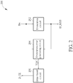
- FIG. 2 is a diagram illustrating a truncator circuit according to an embodiment of the present invention.
- the truncator circuit 110 shown in FIG. 1 may be realized by the truncator circuit 200 shown in FIG. 2 .
- the truncator circuit 200 includes a truncation circuit 202, a truncation error generating circuit 204, and a delay-based circuit 206.
- the truncation circuit 202 truncates the digital signal Do (e.g., N-bit digital word) to generate the digital signal D_MSB (e.g., M-bit digital word, where N>M) .
- the truncation error generating circuit 204 generates the truncation error TQN according to the digital signals Do and D_MSB. For example, the truncation error generating circuit 204 generates the truncation error TQN by subtracting the digital signal D_MSB from the digital signal Do.
- the digital signal D_MSB may be an M-bit most significant bit (MSB) part of the N-bit digital signal Do
- the truncation error TQN may be an (N-M) -bit less significant bit (LSB) part of the N-bit digital signal Do.
- the delay-based circuit 206 outputs the truncation error signal D_TE according to the truncation error TQN.
- the truncator circuit 200 may be a first-order digital delta-sigma truncator when the delay-based circuit 206 has a transfer function "z -1 " in a z-domain.
- the truncator circuit 200 may be a second-order digital delta-sigma truncator when the delay-based circuit 206 has a transfer function "a ⁇ z -1 +b ⁇ z -2 " in a z-domain.
- FIG. 3 is a diagram illustrating a delayed-based circuit according to an embodiment of the present invention.
- the delay-based circuit 206 shown in FIG. 2 may be implemented by the delayed-based circuit 300 shown in FIG. 3 , such that the truncator circuit 200 may be configured to act as a second-order digital delta-sigma truncator.
- the delayed-based circuit 300 includes a plurality of delay circuits 302, 304, a multiplier 306, and a combining circuit 308.
- the truncation error TQN is fed into the delay circuit 302.
- An output of the delay circuit 302 is fed into the multiplier 306 and the delay circuit 304.
- the combining circuit 308 may be an adder that is configured to perform subtraction.
- the truncation error signal D_TE may be generated from subtracting a digital output of the delay circuit 304 from a digital output of the multiplier 306.
- the combining circuit 104 of the delta-sigma modulator 100 is arranged to receive the digital signal Do and the truncation error signal D_TE, and generate the digital output signal Dout by combining the truncation error signal D_TE and the digital signal Do.
- the quantizer circuit 108 outputs the digital signal Do that is indicative of a digital combination result of truncation error compensation signal D_comp, truncation error signal D_TE, and loop-filtered signal V_LF.
- the combining circuit 104 may be an adder that is configured to perform subtraction.
- the quantizer circuit 108 outputs the digital signal Do that is indicative of a digital combination result of truncation error compensation signal D_comp, truncation error signal D_TE, the loop-filtered signal V_LF.
- the loop-filtered signal V_LF is an analog signal
- the truncation error compensation signal D_comp and the truncation error signal D_TE are digital signals.
- the combining circuit 103 is arranged to combining the truncation error compensation signal D_comp and the truncation error signal D_TE to generate a digital signal D_S.
- the digital signal D_S is a summation result generated by adding the truncation error compensation signal D_comp to the truncation error signal D_TE.
- the quantizer circuit 108 includes a successive approximation register (SAR) based quantizer with an internal DAC. Hence, the digital signal D_S can be merged into digital control of the internal DAC of the quantizer circuit 108.
- SAR successive approximation register
- FIG. 4 is a diagram illustrating a SAR quantizer without noise shaping according to an embodiment of the present invention.
- the quantizer circuit 108 shown in FIG. 1 may be implemented using the SAR quantizer 400 shown in FIG. 4 .
- the SAR quantizer 400 includes a track/hold circuit 402, a comparator 404, a SAR control logic 406, a register 408, and an internal DAC 410.
- the track/hold circuit 402 may be controlled according to a sampling frequency. Hence, an analog input voltage V IN is sampled and held on the track/hold circuit 402.
- a reference voltage V DAC is provided from the internal DAC 410 in response to a digital code stored in the register 408, where bits of the digital code is set and adjusted by the SAR control logic 406 according to a comparison result generated from the comparator 404 during an analog-to-digital conversion process. After the conversion of the analog input voltage V IN is complete, the digital word stored in the register 408 is output. As shown in FIG. 4 , the SAR control logic 406 further receives the digital signal D_S that is derived from combining the truncation error signal D_TE and the truncation error compensation signal D_comp. Hence, the digital signal D_S is merged into digital control of the internal DAC 410.
- the digital output of the SAR quantizer 400 is equal to a result of applying analog-to-digital conversion to an analog input voltage derived from combining the analog input voltage V IN and an analog voltage representative of the digital signal D_S.
- the SAR quantizer architecture shown in FIG. 4 is for illustrative purposes only, and is not meant to be a limitation of the present invention.
- the quantizer circuit 108 may be implemented by noise-shaping (NS-SAR) quantizer architecture.
- N-SAR noise-shaping
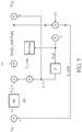
- FIG. 5 is a diagram illustrating a simplified model of the delta-sigma modulator 100 shown in FIG. 1 .
- the truncator circuit 110 is implemented by a first-order digital delta-sigma modulator with a transfer function "z -1 " in the z-domain.
- a noise transfer function (NTF) of the truncator circuit 110 may be simply expressed by (1-z -1 ) .
- the quantization error Q R is induced by the quantizer circuit 108.
- the truncation error Q T can be suppressed in the digital output signal Dout.
- Dout STF DSM ⁇ V IN +NTF DSM ⁇ Q R , where STF DSM represents a signal transfer function of the delta-sigma modulator 100, and NTF DSM represents a noise transfer function of the delta-sigma modulator 100.
- FIG. 6 is a diagram illustrating a frequency response of a noise transfer function of a delta-sigma modulator.
- a noise transfer function of the delta-sigma modulator has a characteristic curve CV1 that is deviated from an ideal characteristic curve CV2.
- the compensation circuit 114 generates the compensation signal D_comp for truncation noise cancellation.
- a noise transfer function of the delta-sigma modulator 100 can be close to or identical to the ideal characteristic curve CV2.
- generation of the digital signal D_MSB only requires processing of the digital signal Do at the truncator circuit 110 (particularly, truncation circuit 202 shown in FIG. 2 ) . That is, an additional combining circuit (e.g., an adder) is not needed by the feedback path for combining the truncation error signal D_TE and an input of the truncator circuit 110. In addition, an additional combining circuit (e.g., an adder) is not needed by the feedforward path for combining the truncation error compensation signal D_comp and an output of the quantizer circuit 108. In this way, the proposed delta-sigma modulator 100 can operate at a higher speed due to shorter loop latency, and the digital hardware of the proposed delta-sigma modulator 100 can be simplified.
- an additional combining circuit e.g., an adder
- the truncation error signal D_TE is not injected to a feedback path, and/or the compensation signal D_comp is not combined with an output of the quantizer circuit 108.
- the quantizer circuit 108 is implemented by a SAR-based quantizer (e.g., SAR quantizer with/without noise shaping)
- the digital signal injection can be merged in the SAR-based quantizer, thereby reducing the hardware cost.
- a quantizer circuit may be implemented by a non-SAR-based quantizer. The same objective of shorting the loop latency and/or simplifying the digital hardware can be achieved.
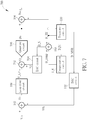
- FIG. 7 is a diagram illustrating a second delta-sigma modulator according to an embodiment of the present invention.
- the major difference between the delta-sigma modulators 100 and 700 is that the delta-sigma modulator 700 employs a non-SAR-based quantizer as a quantization circuit 706, and further includes a combining circuit 702 and a DAC circuit 704.
- the DAC circuit 704 is arranged to receive the digital signal D_S (which is derived from combining the truncation error signal D_TE and the truncation error compensation signal D_comp), and generates an analog signal V2 according to the digital signal D_S.
- the quantizer circuit 706 is arranged to output the digital signal Do that is indicative of a digital combination result of truncation error compensation signal D_TE, truncation error compensation signal D_comp and the loop-filtered signal V_LF.
- the quantizer circuit 706 receives the analog signal V3 (which is indicative of an analog combination result of truncation error compensation signal D_TE, truncation error compensation signal D_comp and the loop-filtered signal V_LF), and generates the digital signal Do according to the analog signal V3.
- the delta-sigma modulator 700 may have the same simplified model as shown in FIG. 5 . Hence, the proposed delta-sigma modulator 700 can operate at a higher speed due to shorter loop latency.
- the truncator circuit 110 may be implemented by a delta-sigma truncator with truncator error shaping.
- a delta-sigma modulator design using the proposed concept that does not combine a truncation error compensation signal at an output of a quantizer circuit falls within the scope of the present invention.
- a quantizer circuit outputs a digital signal that is indicative of a digital combination result of at least a truncation error compensation signal and a loop-filtered signal.
- the present invention may also be defined by means of the following numbered clauses.
Landscapes
- Engineering & Computer Science (AREA)
- Theoretical Computer Science (AREA)
- Compression, Expansion, Code Conversion, And Decoders (AREA)
Abstract
Description
- This application claims the benefit of
U.S. provisional application No.62/818,167 - The present invention relates to delta-sigma modulation, and more particularly, to a delta-sigma modulator with truncation error compensation and an associated method.
- In a conventional delta-sigma modulator with a multi-bit quantizer, a multi-level digital-to-analog converter (DAC) is required to feed back an output signal of the delta-sigma modulator and to work with a loop filter and a quantizer to implement a closed-loop system for noise-shaping function. However, a mismatch between the DAC cells contributes mismatch errors. Since the digital input to the feedback DAC determines the selection of DAC cells included in the feedback DAC, these mismatches result in non-linearity in the analog output of the feedback DAC. A dynamic element matching (DEM) function is a well-known strategy to address the mismatch issue of the multi-level feedback DAC, but the hardware complexity grows exponentially as a bit number of the feedback DAC increases. Thus, there is a need for an innovative feedback DAC reduction technique in a delta-sigma modulator.
- One of the objectives of the claimed invention is to provide a delta-sigma modulator with truncation error compensation and an associated method.
- According to a first aspect of the present invention, an exemplary delta-sigma modulator is disclosed. The exemplary delta-sigma modulator includes a first combining circuit, a loop filter circuit, a quantizer circuit, a truncator circuit, a first digital-to-analog converter (DAC) circuit, and a compensation circuit. The first combining circuit is arranged to receive an analog input signal and an analog feedback signal, and generate a first analog signal by combining the analog feedback signal and the analog input signal. The loop filter circuit is arranged to receive the first analog signal, and generate a loop-filtered signal according to the first analog signal. The quantizer circuit is arranged to output a first digital signal that is indicative of a digital combination result of at least a truncation error compensation signal and the loop-filtered signal. The truncator circuit is arranged to perform truncation upon the first digital signal to generate a second digital signal, wherein a bit number of the second digital signal is smaller than a bit number of the first digital signal. The first DAC circuit is arranged to receive the second digital signal, and generate the analog feedback signal according to the second digital signal. The compensation circuit is arranged to generate the truncation error compensation signal according to a truncation error resulting from said truncation performed upon the first digital signal.
- According to a second aspect of the present invention, an exemplary delta-sigma modulation method is disclosed. The exemplary delta-sigma modulation method includes: generating a first analog signal by combining an analog feedback signal and an analog input signal; generating a loop-filtered signal by applying loop filtering to the first analog signal; performing quantization to output a first digital signal that is indicative of a digital combination result of at least a truncation error compensation signal and the loop-filtered signal; performing truncation upon the first digital signal to generate a second digital signal, wherein a bit number of the second digital signal is smaller than a bit number of the first digital signal; performing digital-to-analog conversion upon the second digital signal to generate the analog feedback signal; and generating the truncation error compensation signal according to a truncation error resulting from said truncation performed upon the first digital signal.
- These and other objectives of the present invention will no doubt become obvious to those of ordinary skill in the art after reading the following detailed description of the preferred embodiment that is illustrated in the various figures and drawings.
-
-
FIG. 1 is a diagram illustrating a first delta-sigma modulator according to an embodiment of the present invention. -
FIG. 2 is a diagram illustrating a truncator circuit according to an embodiment of the present invention. -
FIG. 3 is a diagram illustrating a delayed-based circuit according to an embodiment of the present invention. -
FIG. 4 is a diagram illustrating a SAR quantizer without noise shaping according to an embodiment of the present invention. -
FIG. 5 is a diagram illustrating a simplified model of the delta-sigma modulator shown inFIG. 1 . -
FIG. 6 is a diagram illustrating a frequency response of a noise transfer function of a delta-sigma modulator. -
FIG. 7 is a diagram illustrating a second delta-sigma modulator according to an embodiment of the present invention. - Certain terms are used throughout the following description and claims, which refer to particular components. As one skilled in the art will appreciate, electronic equipment manufacturers may refer to a component by different names. This document does not intend to distinguish between components that differ in name but not in function. In the following description and in the claims, the terms "include" and "comprise" are used in an open-ended fashion, and thus should be interpreted to mean "include, but not limited to ...". Also, the term "couple" is intended to mean either an indirect or direct electrical connection. Accordingly, if one device is coupled to another device, that connection may be through a direct electrical connection, or through an indirect electrical connection via other devices and connections.
-
FIG. 1 is a diagram illustrating a first delta-sigma modulator according to an embodiment of the present invention. By way of example, but not limitation, the delta-sigma modulator 100 may be a part of a delta-sigma analog-to-digital converter (ADC). For example, an analog input signal Vin of the delta-sigma modulator 100 may be an analog input of the delta-sigma ADC, and a digital output of the delta-sigma ADC may be generated by processing a digital output signal Dout of the delta-sigma modulator 100 through a digital filter and a decimation filter. As shown inFIG. 1 , the delta-sigma modulator 100 includes a plurality of combiningcircuits loop filter circuit 106, aquantizer circuit 108, a digital-to-analog converter (DAC)circuit 112, atruncator circuit 110, and acompensation circuit 114. The combiningcircuit 102 is arranged to receive the analog input signal Vin and an analog feedback signal Vfb, and generate an analog signal V1 by combining the analog feedback signal Vfb and the analog input signal Vin. For example, the combiningcircuit 102 outputs a voltage difference between the analog signal V1 and the analog feedback signal Vfb as the analog signal V1 (i.e., V1 = Vin-Vfb). The loop filter circuit is arranged to receive the analog signal V1, and generate a loop-filtered signal V_LF according to the analog signal V1. For example, theloop filter circuit 106 may be implemented by an integrator with a transfer function
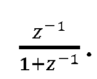
- The
quantizer circuit 108 is arranged to perform quantization to output a digital signal Do that is indicative of a digital combination result of a truncation error compensation signal D_comp (which is a digital signal), a truncation error signal D_TE (which is a digital signal), and the loop-filtered signal V_LF (which is an analog signal). Thetruncator circuit 110 is arranged to perform truncation upon the digital signal Do to generate a digital signal D_MSB, wherein a bit number of the digital signal D_MSB is smaller than a bit number of the digital signal Do. Thetruncator circuit 110 and theDAC circuit 112 are located at a feedback path between thequantizer circuit 108 and the combiningcircuit 102. Hence, theDAC circuit 112 is arranged to receive the digital signal D_MSB, and generate the analog feedback signal Vfb according to the digital signal D_MSB. Thecompensation circuit 114 is arranged to generate the truncation error compensation signal D_comp according to a truncation error TQN resulting from the truncation performed upon the digital signal Do. - In this embodiment, the
truncator circuit 110 may be implemented by a delta-sigma truncator with truncator error shaping.FIG. 2 is a diagram illustrating a truncator circuit according to an embodiment of the present invention. Thetruncator circuit 110 shown inFIG. 1 may be realized by thetruncator circuit 200 shown inFIG. 2 . Thetruncator circuit 200 includes atruncation circuit 202, a truncationerror generating circuit 204, and a delay-basedcircuit 206. Thetruncation circuit 202 truncates the digital signal Do (e.g., N-bit digital word) to generate the digital signal D_MSB (e.g., M-bit digital word, where N>M) . The truncationerror generating circuit 204 generates the truncation error TQN according to the digital signals Do and D_MSB. For example, the truncationerror generating circuit 204 generates the truncation error TQN by subtracting the digital signal D_MSB from the digital signal Do. In this example, the digital signal D_MSB may be an M-bit most significant bit (MSB) part of the N-bit digital signal Do, and the truncation error TQN may be an (N-M) -bit less significant bit (LSB) part of the N-bit digital signal Do. The delay-basedcircuit 206 outputs the truncation error signal D_TE according to the truncation error TQN. For example, thetruncator circuit 200 may be a first-order digital delta-sigma truncator when the delay-basedcircuit 206 has a transfer function "z-1" in a z-domain. For another example, thetruncator circuit 200 may be a second-order digital delta-sigma truncator when the delay-basedcircuit 206 has a transfer function "a∗z-1+b∗z-2" in a z-domain. -
FIG. 3 is a diagram illustrating a delayed-based circuit according to an embodiment of the present invention. The delay-basedcircuit 206 shown inFIG. 2 may be implemented by the delayed-basedcircuit 300 shown inFIG. 3 , such that thetruncator circuit 200 may be configured to act as a second-order digital delta-sigma truncator. As shown inFIG. 3 , the delayed-basedcircuit 300 includes a plurality ofdelay circuits multiplier 306, and a combiningcircuit 308. The truncation error TQN is fed into thedelay circuit 302. An output of thedelay circuit 302 is fed into themultiplier 306 and thedelay circuit 304. The combiningcircuit 308 may be an adder that is configured to perform subtraction. Hence, the truncation error signal D_TE may be generated from subtracting a digital output of thedelay circuit 304 from a digital output of themultiplier 306. - The combining
circuit 104 of the delta-sigma modulator 100 is arranged to receive the digital signal Do and the truncation error signal D_TE, and generate the digital output signal Dout by combining the truncation error signal D_TE and the digital signal Do. As mentioned above, thequantizer circuit 108 outputs the digital signal Do that is indicative of a digital combination result of truncation error compensation signal D_comp, truncation error signal D_TE, and loop-filtered signal V_LF. Since the truncation error signal D_TE is injected to a forward path at which thequantizer circuit 108 is located rather than injected to a feedback path at which thetruncator circuit 110 is located, the delta-sigma modulator 100 has the combiningcircuit 104 that is arranged to subtract the truncation error signal D_TE from the digital signal Do to generate the digital output signal Dout (i.e., Dout = Do-D_TE) . For example, the combiningcircuit 104 may be an adder that is configured to perform subtraction. - The
quantizer circuit 108 outputs the digital signal Do that is indicative of a digital combination result of truncation error compensation signal D_comp, truncation error signal D_TE, the loop-filtered signal V_LF. It should be noted that the loop-filtered signal V_LF is an analog signal, while the truncation error compensation signal D_comp and the truncation error signal D_TE are digital signals. In this embodiment, the combiningcircuit 103 is arranged to combining the truncation error compensation signal D_comp and the truncation error signal D_TE to generate a digital signal D_S. For example, the digital signal D_S is a summation result generated by adding the truncation error compensation signal D_comp to the truncation error signal D_TE. In this embodiment, thequantizer circuit 108 includes a successive approximation register (SAR) based quantizer with an internal DAC. Hence, the digital signal D_S can be merged into digital control of the internal DAC of thequantizer circuit 108. -
FIG. 4 is a diagram illustrating a SAR quantizer without noise shaping according to an embodiment of the present invention. Thequantizer circuit 108 shown inFIG. 1 may be implemented using the SAR quantizer 400 shown inFIG. 4 . The SAR quantizer 400 includes a track/hold circuit 402, acomparator 404, aSAR control logic 406, aregister 408, and aninternal DAC 410. The track/hold circuit 402 may be controlled according to a sampling frequency. Hence, an analog input voltage VIN is sampled and held on the track/hold circuit 402. A reference voltage VDAC is provided from theinternal DAC 410 in response to a digital code stored in theregister 408, where bits of the digital code is set and adjusted by theSAR control logic 406 according to a comparison result generated from thecomparator 404 during an analog-to-digital conversion process. After the conversion of the analog input voltage VIN is complete, the digital word stored in theregister 408 is output. As shown inFIG. 4 , theSAR control logic 406 further receives the digital signal D_S that is derived from combining the truncation error signal D_TE and the truncation error compensation signal D_comp. Hence, the digital signal D_S is merged into digital control of theinternal DAC 410. Though thecomparator 404 receives the analog input voltage VIN, the digital output of the SAR quantizer 400 is equal to a result of applying analog-to-digital conversion to an analog input voltage derived from combining the analog input voltage VIN and an analog voltage representative of the digital signal D_S. - It should be noted that the SAR quantizer architecture shown in
FIG. 4 is for illustrative purposes only, and is not meant to be a limitation of the present invention. For example, thequantizer circuit 108 may be implemented by noise-shaping (NS-SAR) quantizer architecture. To put it simply, the present invention has no limitations on the SAR quantizer architecture employed by thequantizer circuit 108. -
FIG. 5 is a diagram illustrating a simplified model of the delta-sigma modulator 100 shown inFIG. 1 . For clarity and simplicity, it is assumed that thetruncator circuit 110 is implemented by a first-order digital delta-sigma modulator with a transfer function "z-1" in the z-domain. Hence, a noise transfer function (NTF) of thetruncator circuit 110 may be simply expressed by (1-z-1) . The quantization error QR is induced by thequantizer circuit 108. The truncation error QT (TQN=QT) is introduced by thetruncator circuit 110, where an MSB part of the digital signal Do is processed via a feedback path, and an LSB part of the digital signal Do is processed via a compensation path. To achieve truncation error cancellation, thecompensation circuit 114 is arranged to generate the truncation error compensation signal D_comp according to the truncation error TQN and a transfer function Hcomp, where the transfer function Hcomp is set on the basis of the NTF of the delta-sigma truncator and a transfer function H(z) of theloop filter circuit 106. For example, Hcomp = - (1-z-1) ∗H (z) . With a proper setting of the transfer function Hcomp of thecompensation circuit 114, the truncation error QT can be suppressed in the digital output signal Dout. For example, Dout = STFDSM ∗VIN+NTFDSM ∗QR, where STFDSM represents a signal transfer function of the delta-sigma modulator 100, and NTFDSM represents a noise transfer function of the delta-sigma modulator 100. -
FIG. 6 is a diagram illustrating a frequency response of a noise transfer function of a delta-sigma modulator. When no truncation error compensation is employed by a delta-sigma modulator with feedback truncation, a noise transfer function of the delta-sigma modulator has a characteristic curve CV1 that is deviated from an ideal characteristic curve CV2. Regarding the proposed delta-sigma modulator 100, thecompensation circuit 114 generates the compensation signal D_comp for truncation noise cancellation. Hence, with a proper setting of the transfer function Hcomp of thecompensation circuit 114, a noise transfer function of the delta-sigma modulator 100 can be close to or identical to the ideal characteristic curve CV2. - As shown in
FIG. 5 , generation of the digital signal D_MSB only requires processing of the digital signal Do at the truncator circuit 110 (particularly,truncation circuit 202 shown inFIG. 2 ) . That is, an additional combining circuit (e.g., an adder) is not needed by the feedback path for combining the truncation error signal D_TE and an input of thetruncator circuit 110. In addition, an additional combining circuit (e.g., an adder) is not needed by the feedforward path for combining the truncation error compensation signal D_comp and an output of thequantizer circuit 108. In this way, the proposed delta-sigma modulator 100 can operate at a higher speed due to shorter loop latency, and the digital hardware of the proposed delta-sigma modulator 100 can be simplified. - The truncation error signal D_TE is not injected to a feedback path, and/or the compensation signal D_comp is not combined with an output of the
quantizer circuit 108. In a case where thequantizer circuit 108 is implemented by a SAR-based quantizer (e.g., SAR quantizer with/without noise shaping), the digital signal injection can be merged in the SAR-based quantizer, thereby reducing the hardware cost. However, this is for illustrative purposes only, and is not meant to be a limitation of the present invention. Alternatively, a quantizer circuit may be implemented by a non-SAR-based quantizer. The same objective of shorting the loop latency and/or simplifying the digital hardware can be achieved. -
FIG. 7 is a diagram illustrating a second delta-sigma modulator according to an embodiment of the present invention. The major difference between the delta-sigma modulators sigma modulator 700 employs a non-SAR-based quantizer as aquantization circuit 706, and further includes a combiningcircuit 702 and aDAC circuit 704. TheDAC circuit 704 is arranged to receive the digital signal D_S (which is derived from combining the truncation error signal D_TE and the truncation error compensation signal D_comp), and generates an analog signal V2 according to the digital signal D_S. The combiningcircuit 702 is arranged to receive the loop-filtered signal V_LF and the analog signal V2, and generate an analog signal V3 by combining the loop-filtered signal V_LF and the analog signal V2. That is, V3 = V_LF+V2. Like thequantizer circuit 108, thequantizer circuit 706 is arranged to output the digital signal Do that is indicative of a digital combination result of truncation error compensation signal D_TE, truncation error compensation signal D_comp and the loop-filtered signal V_LF. In this embodiment, thequantizer circuit 706 receives the analog signal V3 (which is indicative of an analog combination result of truncation error compensation signal D_TE, truncation error compensation signal D_comp and the loop-filtered signal V_LF), and generates the digital signal Do according to the analog signal V3. The delta-sigma modulator 700 may have the same simplified model as shown inFIG. 5 . Hence, the proposed delta-sigma modulator 700 can operate at a higher speed due to shorter loop latency. - In above embodiments shown in
FIG. 1 andFIG. 7 , thetruncator circuit 110 may be implemented by a delta-sigma truncator with truncator error shaping. However, these are for illustrative purposes only, and are not meant to limitations of the present invention. In practice, any delta-sigma modulator design using the proposed concept that does not combine a truncation error compensation signal at an output of a quantizer circuit falls within the scope of the present invention. For example, a quantizer circuit outputs a digital signal that is indicative of a digital combination result of at least a truncation error compensation signal and a loop-filtered signal. - Those skilled in the art will readily observe that numerous modifications and alterations of the device and method may be made while retaining the teachings of the invention. Accordingly, the above disclosure should be construed as limited only by the metes and bounds of the appended claims.
- The present invention may also be defined by means of the following numbered clauses.
- 1. A delta-sigma modulator comprising:
- a first combining circuit, arranged to receive an analog input signal and an analog feedback signal, and generate a first analog signal by combining the analog feedback signal and the analog input signal;
- a loop filter circuit, arranged to receive the first analog signal, and generate a loop-filtered signal according to the first analog signal;
- a quantizer circuit, arranged to output a first digital signal that is indicative of a digital combination result of at least a truncation error compensation signal and the loop-filtered signal;
- a truncator circuit, arranged to perform truncation upon the first digital signal to generate a second digital signal, wherein a bit number of the second digital signal is smaller than a bit number of the first digital signal;
- a first digital-to-analog converter (DAC) circuit, arranged to receive the second digital signal, and generate the analog feedback signal according to the second digital signal; and
- a compensation circuit, arranged to generate the truncation error compensation signal according to a truncation error resulting from said truncation performed upon the first digital signal.
- 2. The delta-sigma modulator of
clause 1, wherein the quantizer circuit outputs the first digital signal that is indicative of the digital combination result of the truncation error compensation signal, the loop-filtered signal, and a truncation error signal, and the truncator circuit is further arranged to generate the truncation error signal according to the truncation error. - 3. The delta-sigma modulator of clause 2, further comprising:
a second combining circuit, arranged to receive the first digital signal and the truncation error signal, and generate a digital output signal by combining the truncation error signal and the first digital signal. - 4. The delta-sigma modulator of clause 3, wherein the digital output signal is generated by subtracting the truncation error signal from the first digital signal.
- 5. The delta-sigma modulator of clause 2, wherein the truncator circuit is a delta-sigma truncator.
- 6. The delta-sigma modulator of clause 5, wherein the compensation circuit generates the truncation error compensation signal according to the truncation error and a transfer function of the compensation circuit, and the transfer function of the compensation circuit depends on a noise transfer function of the delta-sigma truncator and a transfer function of the loop filter circuit.
- 7. The delta-sigma modulator of
clause 1, further comprising:- a second combining circuit, arranged to receive the truncation error signal and the truncation error compensation signal, and generate a third digital signal by combining at least the truncation error signal and the truncation error compensation signal;
- wherein the quantizer circuit comprises a successive approximation register (SAR) based quantizer with an internal DAC, and the third digital signal is merged into digital control of the internal DAC.
- 8. The delta-sigma modulator of
clause 1, further comprising:- a second combining circuit, arranged to receive the truncation error signal and the truncation error compensation signal, and generate a third digital signal by at least combining the truncation error signal and the truncation error compensation signal; and
- a second DAC circuit, arranged to receive the third digital signal, and generate a second analog signal according to the third digital signal; and
- a third combining circuit, arranged receive the second analog signal and the loop-filtered signal, and generate a third analog signal by combining the second analog signal and the loop-filtered signal;
- wherein the quantizer circuit receives the third analog signal, and generates the first digital signal according to the third analog signal.
- 9. A delta-sigma modulation method comprising:
- generating a first analog signal by combining an analog feedback signal and an analog input signal;
- generating a loop-filtered signal by applying loop filtering to the first analog signal;
- performing quantization to output a first digital signal that is indicative of a digital combination result of at least a truncation error compensation signal and the loop-filtered signal;
- performing truncation upon the first digital signal to generate a second digital signal, wherein a bit number of the second digital signal is smaller than a bit number of the first digital signal;
- performing digital-to-analog conversion upon the second digital signal to generate the analog feedback signal; and
- generating the truncation error compensation signal according to a truncation error resulting from said truncation performed upon the first digital signal.
- 10. The delta-sigma modulation method of clause 9, further comprising:
- generating a truncation error signal according to the truncation error;
- wherein the first digital signal is indicative of the digital combination result of the truncation error compensation signal, the loop-filtered signal, and the truncation error signal.
- 11. The delta-sigma modulation method of clause 10, further comprising:
generating a digital output signal by combining the truncation error signal and the first digital signal. - 12. The delta-sigma modulation method of clause 11, wherein the digital output signal is generated by subtracting the truncation error signal from the first digital signal.
- 13. The delta-sigma modulation method of clause 10, wherein the truncation error signal and the second digital signal are generated from delta-sigma truncation.
- 14. The delta-sigma modulation method of clause 13, wherein the truncation error compensation signal is generated according to the truncation error and a transfer function of truncation error compensation, and the transfer function of truncation error compensation depends on a noise transfer function of said delta-sigma truncation and a transfer function of said loop filtering.
- 15. The delta-sigma modulation method of clause 9, further comprising:
- generating a third digital signal by combining at least the truncation error signal and the truncation error compensation signal;
- wherein said quantization is performed by a successive approximation register (SAR) based quantizer with an internal DAC, and the third digital signal is merged into digital control of the internal DAC.
- 16. The delta-sigma modulation method of clause 9, further comprising:
- generating a third digital signal by combining at least the truncation error signal and the truncation error compensation signal; and
- performing digital-to-analog conversion upon the third digital signal to generate a second analog signal; and
- generating a third analog signal by combining the second analog signal and the loop-filtered signal;
- wherein performing quantization to output the first digital signal comprises:
generating the first digital signal by performing said quantization upon the third analog signal.
Claims (15)
- A delta-sigma modulator (100, 700) comprising:a first combining circuit (102), arranged to receive an analog input signal and an analog feedback signal, and generate a first analog signal by combining the analog feedback signal and the analog input signal;a loop filter circuit (106), arranged to receive the first analog signal, and generate a loop-filtered signal according to the first analog signal;a quantizer circuit (108, 400), arranged to output a first digital signal that is indicative of a digital combination result of at least a truncation error compensation signal and the loop-filtered signal;a truncator circuit (110, 200), arranged to perform truncation upon the first digital signal to generate a second digital signal, wherein a bit number of the second digital signal is smaller than a bit number of the first digital signal;a first digital-to-analog converter, DAC, circuit(112), arranged to receive the second digital signal, and generate the analog feedback signal according to the second digital signal; anda compensation circuit (114), arranged to generate the truncation error compensation signal according to a truncation error resulting from said truncation performed upon the first digital signal.
- The delta-sigma modulator (100, 700) of claim 1, wherein the quantizer circuit (108, 400) outputs the first digital signal that is indicative of the digital combination result of the truncation error compensation signal, the loop-filtered signal, and a truncation error signal, and the truncator circuit (110, 200) is further arranged to generate the truncation error signal according to the truncation error.
- The delta-sigma modulator (100, 700) of claim 2, further comprising:
a second combining circuit (103), arranged to receive the first digital signal and the truncation error signal, and generate a digital output signal by combining the truncation error signal and the first digital signal. - The delta-sigma modulator (100, 700) of claim 3, wherein the digital output signal is generated by subtracting the truncation error signal from the first digital signal.
- The delta-sigma modulator (100, 700) of claim 2, wherein the truncator circuit (110, 200) is a delta-sigma truncator.
- The delta-sigma modulator (100, 700) of claim 5, wherein the compensation circuit (114) generates the truncation error compensation signal according to the truncation error and a transfer function of the compensation circuit (114), and the transfer function of the compensation circuit (114) depends on a noise transfer function of the delta-sigma truncator and a transfer function of the loop filter circuit (106).
- The delta-sigma modulator (100, 700) of claim 1, further comprising:a second combining circuit (103), arranged to receive the truncation error signal and the truncation error compensation signal, and generate a third digital signal by combining at least the truncation error signal and the truncation error compensation signal;wherein the quantizer circuit (108, 400) comprises a successive approximation register, SAR, based quantizer with an internal DAC, and the third digital signal is merged into digital control of the internal DAC.
- The delta-sigma modulator (100, 700) of claim 1, further comprising:a second combining circuit (103), arranged to receive the truncation error signal and the truncation error compensation signal, and generate a third digital signal by at least combining the truncation error signal and the truncation error compensation signal; anda second DAC circuit (704), arranged to receive the third digital signal, and generate a second analog signal according to the third digital signal; anda third combining circuit 9104), arranged receive the second analog signal and the loop-filtered signal, and generate a third analog signal by combining the second analog signal and the loop-filtered signal;wherein the quantizer circuit (108, 400) receives the third analog signal, and generates the first digital signal according to the third analog signal.
- A delta-sigma modulation method comprising:generating a first analog signal by combining an analog feedback signal and an analog input signal;generating a loop-filtered signal by applying loop filtering to the first analog signal;performing quantization to output a first digital signal that is indicative of a digital combination result of at least a truncation error compensation signal and the loop-filtered signal;performing truncation upon the first digital signal to generate a second digital signal, wherein a bit number of the second digital signal is smaller than a bit number of the first digital signal;performing digital-to-analog conversion upon the second digital signal to generate the analog feedback signal; andgenerating the truncation error compensation signal according to a truncation error resulting from said truncation performed upon the first digital signal.
- The delta-sigma modulation method of claim 9, further comprising:generating a truncation error signal according to the truncation error;wherein the first digital signal is indicative of the digital combination result of the truncation error compensation signal, the loop-filtered signal, and the truncation error signal.
- The delta-sigma modulation method of claim 10, further comprising: generating a digital output signal by combining the truncation error signal and the first digital signal.
- The delta-sigma modulation method of claim 11, wherein the digital output signal is generated by subtracting the truncation error signal from the first digital signal.
- The delta-sigma modulation method of claim 10, wherein the truncation error signal and the second digital signal are generated from delta-sigma truncation.
- The delta-sigma modulation method of claim 13, wherein the truncation error compensation signal is generated according to the truncation error and a transfer function of truncation error compensation, and the transfer function of truncation error compensation depends on a noise transfer function of said delta-sigma truncation and a transfer function of said loop filtering.
- The delta-sigma modulation method of claim 9, further comprising:generating a third digital signal by combining at least the truncation error signal and the truncation error compensation signal;wherein said quantization is performed by a successive approximation register, SAR, based quantizer with an internal DAC, and the third digital signal is merged into digital control of the internal DAC orfurther comprising:generating a third digital signal by combining at least the truncation error signal and the truncation error compensation signal; andperforming digital-to-analog conversion upon the third digital signal to generate a second analog signal; andgenerating a third analog signal by combining the second analog signal and the loop-filtered signal;wherein performing quantization to output the first digital signal comprises:
generating the first digital signal by performing said quantization upon the third analog signal.
Applications Claiming Priority (2)
| Application Number | Priority Date | Filing Date | Title |
|---|---|---|---|
| US201962818167P | 2019-03-14 | 2019-03-14 | |
| US16/809,535 US10979069B2 (en) | 2019-03-14 | 2020-03-04 | Delta-sigma modulator with truncation error compensation and associated method |
Publications (1)
| Publication Number | Publication Date |
|---|---|
| EP3709518A1 true EP3709518A1 (en) | 2020-09-16 |
Family
ID=69780069
Family Applications (1)
| Application Number | Title | Priority Date | Filing Date |
|---|---|---|---|
| EP20161567.1A Ceased EP3709518A1 (en) | 2019-03-14 | 2020-03-06 | Delta-sigma modulator with truncation error compensation and associated method |
Country Status (4)
| Country | Link |
|---|---|
| US (1) | US10979069B2 (en) |
| EP (1) | EP3709518A1 (en) |
| CN (1) | CN111697972B (en) |
| TW (1) | TWI757699B (en) |
Cited By (2)
| Publication number | Priority date | Publication date | Assignee | Title |
|---|---|---|---|---|
| US11563444B1 (en) * | 2021-09-09 | 2023-01-24 | Textron Systems Corporation | Suppressing spurious signals in direct-digital synthesizers |
| EP4329201A1 (en) * | 2022-08-04 | 2024-02-28 | Nxp B.V. | System and method of reducing delta-sigma modulator error using force-and-correction |
Families Citing this family (6)
| Publication number | Priority date | Publication date | Assignee | Title |
|---|---|---|---|---|
| FR3105897B1 (en) * | 2019-12-26 | 2023-10-27 | Thales Sa | Analog-to-digital conversion device comprising two cascaded analog-to-digital conversion stages with successive approximation register and noise shaping, and associated electronic sensor |
| CN113489495B (en) * | 2021-08-17 | 2022-11-01 | 加特兰微电子科技(上海)有限公司 | Signal modulator, integrated circuit, radio device, and electronic apparatus |
| US11870453B2 (en) * | 2021-11-22 | 2024-01-09 | Taiwan Semiconductor Manufacturing Company, Ltd. | Circuits and methods for a noise shaping analog to digital converter |
| US12463656B2 (en) * | 2023-02-23 | 2025-11-04 | Daegu Gyeongbuk Institute Of Science And Technology | Current-to-digital converter with wide dynamic range |
| TWI914753B (en) | 2024-03-27 | 2026-02-11 | 瑞昱半導體股份有限公司 | Radio frequency transceiver circuits and associated circuit set |
| CN119070826B (en) * | 2024-11-04 | 2025-02-25 | 秦玄汉(苏州)信息科技有限公司 | A V/I analog signal transmission system and method based on sigma-delta |
Citations (2)
| Publication number | Priority date | Publication date | Assignee | Title |
|---|---|---|---|---|
| US20170353192A1 (en) * | 2016-06-03 | 2017-12-07 | Mediatek Inc. | Analog-to-digital converter with embedded noise-shaped truncation, embedded noise-shaped segmentation and/or embedded excess loop delay compensation |
| EP3280055A1 (en) * | 2016-08-05 | 2018-02-07 | MediaTek Inc. | Delta-sigma modulator with delta-sigma truncator and associated method for reducing leakage errors of delta-sigma modulator |
Family Cites Families (16)
| Publication number | Priority date | Publication date | Assignee | Title |
|---|---|---|---|---|
| JP2937624B2 (en) * | 1992-05-29 | 1999-08-23 | 日本電気株式会社 | Integrated circuit for digitized quadrature modulation and its inspection method |
| US5493343A (en) * | 1994-12-28 | 1996-02-20 | Thomson Consumer Electronics, Inc. | Compensation for truncation error in a digital video signal decoder |
| US5682161A (en) * | 1996-05-20 | 1997-10-28 | General Electric Company | High-order delta sigma modulator |
| JP3830924B2 (en) * | 2003-07-04 | 2006-10-11 | 松下電器産業株式会社 | Cascaded delta-sigma modulator |
| US6967608B1 (en) * | 2004-06-25 | 2005-11-22 | Texas Instruments Incorporated | Sigma-delta analog-to-digital converter (ADC) with truncation error cancellation in a multi-bit feedback digital-to-analog converter (DAC) |
| US7362247B2 (en) * | 2005-05-06 | 2008-04-22 | Agere Systems Inc. | Digital correction of nonlinearity errors of multibit delta-sigma digital to analog converters |
| US7525464B2 (en) * | 2007-05-29 | 2009-04-28 | National Semiconductor Corporation | Sigma-delta modulator with DAC resolution less than ADC resolution |
| US7450047B1 (en) * | 2007-09-06 | 2008-11-11 | National Semiconductor Corporation | Sigma-delta modulator with DAC resolution less than ADC resolution and increased dynamic range |
| US7961129B2 (en) * | 2009-08-12 | 2011-06-14 | Infineon Technologies Ag | Coupled delta-sigma modulators |
| CN102270990B (en) * | 2010-06-01 | 2013-09-25 | 北京大学深圳研究生院 | Modulator and designing method thereof |
| US8344921B2 (en) * | 2010-11-04 | 2013-01-01 | Mediatek Inc. | Sigma-delta modulator with SAR ADC and truncater having order lower than order of integrator and related sigma-delta modulation method |
| TW201246804A (en) * | 2011-05-05 | 2012-11-16 | Univ Nat Taiwan | Delta-sigma ADC modulator with excess loop delay compensation |
| US9344271B1 (en) * | 2014-03-25 | 2016-05-17 | Microsemi Storage Solutions (U.S.), Inc. | Digital correction of spurious tones caused by a phase detector of a hybrid analog-digital delta-sigma modulator based fractional-N phase locked loop |
| US9490835B2 (en) * | 2014-06-10 | 2016-11-08 | Mediatek Inc. | Modulation circuit and modulation method with digital ELD compensation |
| US9634687B2 (en) * | 2015-06-10 | 2017-04-25 | Mediatek Inc. | VCO-based continuous-time sigma delta modulator equipped with truncation circuit and phase-domain excess loop delay compensation |
| US10141948B2 (en) * | 2016-06-06 | 2018-11-27 | Mediatek Inc. | Delta-sigma modulator, analog-to-digital converter and associated signal conversion method based on multi stage noise shaping structure |
-
2020
- 2020-03-04 US US16/809,535 patent/US10979069B2/en active Active
- 2020-03-05 TW TW109107286A patent/TWI757699B/en active
- 2020-03-06 EP EP20161567.1A patent/EP3709518A1/en not_active Ceased
- 2020-03-12 CN CN202010169347.4A patent/CN111697972B/en active Active
Patent Citations (2)
| Publication number | Priority date | Publication date | Assignee | Title |
|---|---|---|---|---|
| US20170353192A1 (en) * | 2016-06-03 | 2017-12-07 | Mediatek Inc. | Analog-to-digital converter with embedded noise-shaped truncation, embedded noise-shaped segmentation and/or embedded excess loop delay compensation |
| EP3280055A1 (en) * | 2016-08-05 | 2018-02-07 | MediaTek Inc. | Delta-sigma modulator with delta-sigma truncator and associated method for reducing leakage errors of delta-sigma modulator |
Non-Patent Citations (4)
| Title |
|---|
| HE LIN ET AL: "Digital Noise-Coupling Technique for Delta-Sigma Modulators With Segmented Quantiza", IEEE TRANSACTIONS ON CIRCUITS AND SYSTEMS II: EXPRESS BRIEFS, IEEE, US, vol. 61, no. 6, 1 June 2014 (2014-06-01), pages 403 - 407, XP011551104, ISSN: 1549-7747, [retrieved on 20140612], DOI: 10.1109/TCSII.2014.2319994 * |
| LESLIE T.C. ET AL: "An improved sigma-delta modulator architecture", IEEE INTERNATIONAL SYMPOSIUM ON CIRCUITS AND SYSTEMS, 1 May 1990 (1990-05-01), New Orleans, LA, USA, pages 372 - 375, XP093177598, Retrieved from the Internet <URL:https://ieeexplore.ieee.org/stampPDF/getPDF.jsp?tp=&arnumber=112045&ref=aHR0cHM6Ly9pZWVleHBsb3JlLmllZWUub3JnL2RvY3VtZW50LzExMjA0NQ==> DOI: 10.1109/ISCAS.1990.112045 * |
| TSAI HUNG-CHIEH ET AL: "A 64-fJ/Conv.-Step Continuous-Time $\Sigma \Delta$ Modulator in 40-nm CMOS Using Asynchronous SAR Quantizer and Digital $\Delta \Sigma$ Truncator", IEEE JOURNAL OF SOLID-STATE CIRCUITS, IEEE, USA, vol. 48, no. 11, 1 November 2013 (2013-11-01), pages 2637 - 2648, XP011531071, ISSN: 0018-9200, [retrieved on 20131021], DOI: 10.1109/JSSC.2013.2274852 * |
| YAN HAIYUE ET AL: "A second-order continuous-time delta-sigma modulator with double self noise coupling", ANALOG INTEGRATED CIRCUITS AND SIGNAL PROCESSING, SPRINGER NEW YORK LLC, US, vol. 99, no. 2, 20 February 2019 (2019-02-20), pages 251 - 259, XP036767815, ISSN: 0925-1030, [retrieved on 20190220], DOI: 10.1007/S10470-019-01425-X * |
Cited By (3)
| Publication number | Priority date | Publication date | Assignee | Title |
|---|---|---|---|---|
| US11563444B1 (en) * | 2021-09-09 | 2023-01-24 | Textron Systems Corporation | Suppressing spurious signals in direct-digital synthesizers |
| EP4329201A1 (en) * | 2022-08-04 | 2024-02-28 | Nxp B.V. | System and method of reducing delta-sigma modulator error using force-and-correction |
| US12015426B2 (en) | 2022-08-04 | 2024-06-18 | Nxp B.V. | System and method of reducing delta-sigma modulator error using force-and-correction |
Also Published As
| Publication number | Publication date |
|---|---|
| TWI757699B (en) | 2022-03-11 |
| TW202101916A (en) | 2021-01-01 |
| CN111697972A (en) | 2020-09-22 |
| US20200295776A1 (en) | 2020-09-17 |
| US10979069B2 (en) | 2021-04-13 |
| CN111697972B (en) | 2023-09-15 |
Similar Documents
| Publication | Publication Date | Title |
|---|---|---|
| US10979069B2 (en) | Delta-sigma modulator with truncation error compensation and associated method | |
| EP3252953B1 (en) | Analog-to-digital converter with embedded noise-shaped truncation, embedded noise-shaped segmentation and/or embedded excess loop delay compensation | |
| EP2351228B1 (en) | Method and apparatus for dithering in multi-bit sigma-delta digital-to-analog converters | |
| JP5496399B2 (en) | Sigma delta modulator with shortening and its application | |
| US8928511B2 (en) | Sigma-delta modulator with SAR ADC and truncater and related sigma-delta modulation method | |
| US7129874B2 (en) | Method and apparatus for operating a pipelined ADC circuit | |
| US5977899A (en) | Digital-to-analog converter using noise-shaped segmentation | |
| US8120518B2 (en) | Digital feedforward sigma-delta modulator in analog-to-digital converter and modulation method thereof | |
| US6304608B1 (en) | Multibit sigma-delta converters employing dynamic element matching with reduced baseband tones | |
| US20110032132A1 (en) | Delta-sigma analog-to-digital conversion apparatus and method thereof | |
| US10432214B2 (en) | Apparatus for applying different transfer functions to code segments of multi-bit output code that are sequentially determined and output by multi-bit quantizer and associated delta-sigma modulator | |
| JP4543209B2 (en) | Multistage converter using digital dither | |
| US7084791B2 (en) | Analog-to-digital converter with correction of offset errors | |
| US6100834A (en) | Recursive multi-bit ADC with predictor | |
| US10374626B2 (en) | Interleaving quantizer in continuous-time delta-sigma modulator for quantization level increment | |
| US6535154B1 (en) | Enhanced noise-shaped quasi-dynamic-element-matching technique | |
| KR102441025B1 (en) | Semiconductor device and operating method thereof | |
| US5936561A (en) | Apparatus and methods for digitally compensated multi-bit sigma-delta analog-to-digital conversion | |
| US7385537B2 (en) | Linear feedback shift register first-order noise generator |
Legal Events
| Date | Code | Title | Description |
|---|---|---|---|
| PUAI | Public reference made under article 153(3) epc to a published international application that has entered the european phase |
Free format text: ORIGINAL CODE: 0009012 |
|
| STAA | Information on the status of an ep patent application or granted ep patent |
Free format text: STATUS: THE APPLICATION HAS BEEN PUBLISHED |
|
| AK | Designated contracting states |
Kind code of ref document: A1 Designated state(s): AL AT BE BG CH CY CZ DE DK EE ES FI FR GB GR HR HU IE IS IT LI LT LU LV MC MK MT NL NO PL PT RO RS SE SI SK SM TR |
|
| AX | Request for extension of the european patent |
Extension state: BA ME |
|
| STAA | Information on the status of an ep patent application or granted ep patent |
Free format text: STATUS: REQUEST FOR EXAMINATION WAS MADE |
|
| 17P | Request for examination filed |
Effective date: 20210119 |
|
| RBV | Designated contracting states (corrected) |
Designated state(s): AL AT BE BG CH CY CZ DE DK EE ES FI FR GB GR HR HU IE IS IT LI LT LU LV MC MK MT NL NO PL PT RO RS SE SI SK SM TR |
|
| STAA | Information on the status of an ep patent application or granted ep patent |
Free format text: STATUS: EXAMINATION IS IN PROGRESS |
|
| 17Q | First examination report despatched |
Effective date: 20211112 |
|
| P01 | Opt-out of the competence of the unified patent court (upc) registered |
Effective date: 20230607 |
|
| STAA | Information on the status of an ep patent application or granted ep patent |
Free format text: STATUS: THE APPLICATION HAS BEEN REFUSED |
|
| 18R | Application refused |
Effective date: 20241130 |