EP3706338A1 - Transmission/reception circuit, communication device, and method for controlling transmission/reception circuit - Google Patents
Transmission/reception circuit, communication device, and method for controlling transmission/reception circuit Download PDFInfo
- Publication number
- EP3706338A1 EP3706338A1 EP18873604.5A EP18873604A EP3706338A1 EP 3706338 A1 EP3706338 A1 EP 3706338A1 EP 18873604 A EP18873604 A EP 18873604A EP 3706338 A1 EP3706338 A1 EP 3706338A1
- Authority
- EP
- European Patent Office
- Prior art keywords
- signal
- transmission
- circuit
- reception
- loop
- Prior art date
- Legal status (The legal status is an assumption and is not a legal conclusion. Google has not performed a legal analysis and makes no representation as to the accuracy of the status listed.)
- Granted
Links
Images






Classifications
-
- H—ELECTRICITY
- H04—ELECTRIC COMMUNICATION TECHNIQUE
- H04B—TRANSMISSION
- H04B17/00—Monitoring; Testing
- H04B17/10—Monitoring; Testing of transmitters
- H04B17/11—Monitoring; Testing of transmitters for calibration
- H04B17/14—Monitoring; Testing of transmitters for calibration of the whole transmission and reception path, e.g. self-test loop-back
-
- H—ELECTRICITY
- H04—ELECTRIC COMMUNICATION TECHNIQUE
- H04B—TRANSMISSION
- H04B17/00—Monitoring; Testing
- H04B17/20—Monitoring; Testing of receivers
- H04B17/29—Performance testing
- H04B17/295—Detection of non-compliance or faulty performance, e.g. response deviations
-
- H—ELECTRICITY
- H04—ELECTRIC COMMUNICATION TECHNIQUE
- H04B—TRANSMISSION
- H04B17/00—Monitoring; Testing
- H04B17/0082—Monitoring; Testing using service channels; using auxiliary channels
- H04B17/0085—Monitoring; Testing using service channels; using auxiliary channels using test signal generators
Definitions
- the present technology has an excellent effect of executing a loop-back test during wireless transmission in a circuit that performs wireless communication. Note that the effect disclosed herein is not necessarily limited and may be any effect disclosed in the present disclosure.
- the signal processing unit 120 performs predetermined signal processing on an information signal.
- the signal processing unit 120 performs signal processing such as coding to generate a transmission information signal and supplies the transmission information signal to the transmission/reception circuit 200. Further, the signal processing unit 120 receives a reception information signal from the transmission/reception circuit 200 and performs signal processing such as decoding on the signal.
- the information signals such as the transmission information signal and the reception information signal are, for example, pulse signals on which data is superimposed.
- the selector 211 selects one of the selector 212 or the transmission circuit 240, and connects the selected one to the antenna 110 in response to a selection signal SELa from the signal processing unit 120.
- the transmission/reception circuit 200 performs wireless communication while switching between transmission and reception by, for example, time-division. For a certain unit time allocated for transmission, the signal processing unit 120 controls the selector 211 so as to connect the transmission circuit 240 to the antenna 110 in response to the selection signal SELa. Thus, a transmission signal is output to the antenna 110 from the transmission circuit 240. This unit time is referred to as "time slot".
- the reception circuit 220 includes a mixer 221 and a low-noise amplifier 222.
- the low-noise amplifier 222 amplifies the signal to be demodulated from the selector 212 and supplies the signal to be demodulated to the signal processing unit 120.
- the mixer 221 mixes the local signal from the local oscillator 260 and the amplified signal to be demodulated, thereby generating a reception information signal, and supplies the reception information signal to the low-noise amplifier 222.
- the reception information signal having the frequency f pr can be obtained because of the mixture of the local signal.
- Fig. 6 is a circuit diagram showing a configuration example of the phase shifter 270 in the second embodiment of the present technology.
- the phase shifter 270 includes a predetermined number of (e.g., five) delay circuits 271 and a multiplexer 272.
- a configuration of the transmission circuit 240 in the fifth embodiment is similar to that in the fourth embodiment.
- a configuration of the loop-back test signal generation circuit 230 in the fifth embodiment is similar to that in the fourth embodiment, except that a local signal is modulated instead of a transmission signal.
- a configuration of the reception circuit 220 in the fifth embodiment is similar to that in the fourth embodiment. Note that a phase and frequency of a local signal generated by the local oscillator 223 is similar to those of the local signal generated by the local oscillator 260.
- IoT Internet of things
- IoT is a mechanism in which an IoT device 9100 that is a "thing" is connected to another IoT device 9003, the Internet, a cloud 9005, and the like and exchanges information to control each other.
- IoT can be used in various industries such as agriculture, houses, automobiles, manufacture, distribution, and energy.
- a communication method of the IoT device 9001 in a house is desirably a low-power-consumption communication method. Further, the IoT device 9001 may perform communication via WiFi inside the house and via 3G/LTE outside the house.
- An external server 9006 for controlling the IoT device may be installed in the cloud 9005 to control the IoT device 9001.
- the IoT device 9001 transmits data such as a situation of a home appliance, temperature, humidity, energy consumption, and presence/absence of a person/animal inside/outside the house. Data transmitted from the home appliances is accumulated in the external server 9006 via the cloud 9005. A new service is provided on the basis of such data.
- Such an IoT device 9001 can be controlled by audio with the use of an audio recognition technology.
Landscapes
- Physics & Mathematics (AREA)
- Electromagnetism (AREA)
- Engineering & Computer Science (AREA)
- Computer Networks & Wireless Communication (AREA)
- Signal Processing (AREA)
- Transceivers (AREA)
- Monitoring And Testing Of Transmission In General (AREA)
Abstract
Description
- The present technology relates to a transmission/reception circuit, a communication apparatus, and a method of controlling the transmission/reception circuit. More specifically, the present technology relates to a transmission/reception circuit that performs carrier communication, a communication apparatus, and a method of controlling the transmission/reception circuit.
- Conventionally, in wireless communication, carrier communication in which modulation and demodulation are performed by using a carrier wave such as a local signal is widely used. In addition, in a transmission/reception circuit that performs carrier communication, a loop-back test for transmitting a test signal to a reception circuit from a transmission circuit not via an antenna is performed in some cases, in order to determine whether or not the reception circuit normally operates. For example, there is proposed a circuit including a selector that separates the transmission circuit and the reception circuit from the antenna and directly connects the transmission circuit and the reception circuit at the time of the loop-back test (see, for example, Patent Document 1). In this circuit, the selector selects one of the transmission circuit or the reception circuit and connects the selected circuit to the antenna at the time of wireless communication. Further, in this circuit, the transmission circuit and the reception circuit share the same local oscillator.
- Patent Document 1: Japanese Patent Application Laid-Open No.
2009-060174 - In the related art described above, because the transmission circuit and the reception circuit share the local oscillator, a circuit scale and costs can be reduced, as compared to a case where those circuits individually include a local oscillator. However, in the related art described above, the transmission circuit and the reception circuit are not directly connected and are connected to the antenna at the time of wireless transmission. Thus, there is an issue that the loop-back test cannot be executed during wireless transmission.
- The present technology has been made in view of such a circumstance, and an object thereof is to execute a loop-back test during wireless transmission in a circuit that performs wireless communication.
- The present technology is made in order to solve the above issue and a first aspect of the present technology is a transmission/reception circuit and a control method thereof including: a transmission circuit that modulates a transmission information signal and supplies the transmission information signal, as a transmission signal, to an antenna; a loop-back test signal generation circuit that modulates a predetermined signal to be modulated and supplies the predetermined signal to be modulated as a loop-back test signal; a selection unit that selects one of a reception signal from the antenna or the loop-back test signal, and supplies the selected signal as a signal to be demodulated; a reception circuit that demodulates the signal to be demodulated and acquires a reception information signal; and a test circuit that compares the reception information signal and the predetermined signal to be modulated.
- With this configuration, while the transmission circuit can supply a transmission signal, a loop-back test signal can be generated.
- In addition, in the first aspect includes a local oscillator that generates a predetermined local signal and supplies the predetermined local signal to the transmission circuit and the loop-back test signal generation circuit, in which the transmission circuit mixes the predetermined local signal and the transmission information signal, and the loop-back test signal generation circuit mixes the predetermined local signal and the predetermined signal to be modulated. With this configuration, the transmission circuit and the loop-back test signal generation circuit can share the local oscillator.
- In addition, in the first aspect, the local oscillator may further transmit the predetermined local signal to the reception circuit, and the reception circuit may mix the predetermined local signal and the signal to be demodulated. With this configuration, the transmission circuit, the loop-back test signal generation circuit, and the reception circuit can share the local oscillator.
- In addition, the first aspect may further include a phase shifter that corrects a phase error of the predetermined local signal and supplies the predetermined local signal to the reception circuit, and the local oscillator may supply the predetermined local signal to the reception circuit via the phase shifter. With this configuration, the phase error of the local signal can be corrected.
- In addition, in the first aspect, the transmission circuit may include: a first local oscillator that generates a first local signal, and a first mixer that mixes the first local signal and the transmission information signal; and the reception circuit may include a second local oscillator that generates a second local signal, and a second mixer that mixes the second local signal and the signal to be demodulated. With this configuration, the phase error of the local signal can be restrained.
- In addition, in the first aspect, the loop-back test signal generation circuit may include a third local oscillator that generates a third local signal, and a third mixer that mixes the third local signal and the predetermined signal to be modulated. With this configuration, the phase error of the local signal can be restrained.
- In addition, in the first aspect, the transmission circuit may supply the transmission signal to the antenna and supply the transmission signal, as the predetermined signal to be modulated, to the loop-back test signal generation circuit. With this configuration, the local oscillator of the transmission circuit can be omitted.
- In addition, a second aspect of the present technology is a communication apparatus including: a transmission circuit that modulates a transmission information signal and supplies the transmission information signal, as a transmission signal, to an antenna; the antenna that transmits the transmission signal and receives a reception signal; a loop-back test signal generation circuit that modulates a predetermined signal to be modulated and supplies the predetermined signal to be modulated as a loop-back test signal; a selection unit that selects one of the reception signal from the antenna or the loop-back test signal, and supplies the selected signal as a signal to be demodulated; a reception circuit that demodulates the signal to be demodulated and acquires a reception information signal; and a test circuit that compares the reception information signal and the predetermined signal to be modulated. With this configuration, while the transmission circuit can supply a transmission signal to the antenna, a loop-back test signal can be generated.
- The present technology has an excellent effect of executing a loop-back test during wireless transmission in a circuit that performs wireless communication. Note that the effect disclosed herein is not necessarily limited and may be any effect disclosed in the present disclosure.
-
-
Fig. 1 is a block diagram showing a configuration example of a communication apparatus in a first embodiment of the present technology. -
Fig. 2 is a block diagram showing a configuration example of a transmission/reception circuit in the first embodiment of the present technology. -
Fig. 3 is circuit diagrams showing configuration examples of a transmission circuit, a loop-back test signal generation circuit, and a reception circuit in the first embodiment of the present technology. -
Fig. 4 is a flowchart showing an example of operation of a transmission/reception circuit in the first embodiment of the present technology. -
Fig. 5 is a block diagram showing a configuration example of a transmission/reception circuit in the second embodiment of the present technology. -
Fig. 6 is a circuit diagram showing a configuration example of a phase shifter in a second embodiment of the present technology. -
Fig. 7 is a block diagram showing a configuration example of a transmission/reception circuit in a third embodiment of the present technology. -
Fig. 8 is circuit diagrams showing configuration examples of a transmission circuit, a loop-back test signal generation circuit, and a reception circuit in the third embodiment of the present technology. -
Fig. 9 is a block diagram showing a configuration example of a transmission/reception circuit in a fourth embodiment of the present technology. -
Fig. 10 is circuit diagrams showing configuration examples of a transmission circuit, a loop-back test signal generation circuit, and a reception circuit in the fourth embodiment of the present technology. -
Fig. 11 is a block diagram showing a configuration example of a transmission/reception circuit in a fifth embodiment of the present technology. -
Fig. 12 is circuit diagrams showing configuration examples of a transmission circuit, a loop-back test signal generation circuit, and a reception circuit in the fifth embodiment of the present technology. -
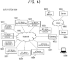
Fig. 13 shows an example of a schematic configuration of an Internet of Things (IoT) system to which a technology according to the present disclosure is applicable. - Hereinafter, modes for carrying out the present technology (hereinafter, referred to as "embodiments") will be described. Description will be made in the following order.
- 1. First embodiment (example where a loop-back test signal generation circuit generates a test signal)
- 2. Second embodiment (example where a phase error is corrected and a loop-back test signal generation circuit generates a test signal)
- 3. Third embodiment (example where a local oscillator is not shared, and a loop-back test signal generation circuit generates a test signal)
- 4. Fourth embodiment (example where a loop-back test signal generation circuit generates a test signal on the basis of a transmission signal)
- 5. Fifth embodiment (example where a loop-back test signal generation circuit that shares a local oscillator with a transmission circuit generates a test signal)
- 6. Application examples
-
Fig. 1 is a block diagram showing a configuration example of acommunication apparatus 100 in a first embodiment of the present technology. Thecommunication apparatus 100 performs wireless communication and includes anantenna 110, a transmission/reception circuit 200, and asignal processing unit 120. Thecommunication apparatus 100 is expected to be, for example, a smartphone or an IoT device. - The
antenna 110 converts an electromagnetic wave into an electric signal and vice versa. Theantenna 110 converts (i.e., receives) an electromagnetic wave into an electric signal and supplies the electric signal, as a reception signal, to the transmission/reception circuit 200 via asignal line 119. Further, theantenna 110 converts (i.e., transmits) a transmission signal that is an electric signal received from the transmission/reception circuit 200 via thesignal line 119 into an electromagnetic wave. - The transmission/
reception circuit 200 modulates and demodulates a signal. The transmission/reception circuit 200 modulates a transmission information signal that is an information signal received from thesignal processing unit 120 via asignal line 129 and supplies the transmission information signal, as a transmission signal, to theantenna 110. Further, the transmission/reception circuit 200 demodulates a reception signal from theantenna 110, extracts an information signal as a reception information signal, and supplies the information signal to thesignal processing unit 120 via thesignal line 129. - The
signal processing unit 120 performs predetermined signal processing on an information signal. Thesignal processing unit 120 performs signal processing such as coding to generate a transmission information signal and supplies the transmission information signal to the transmission/reception circuit 200. Further, thesignal processing unit 120 receives a reception information signal from the transmission/reception circuit 200 and performs signal processing such as decoding on the signal. The information signals such as the transmission information signal and the reception information signal are, for example, pulse signals on which data is superimposed. -
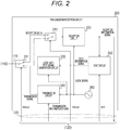
Fig. 2 is a block diagram showing a configuration example of the transmission/reception circuit 200 in the first embodiment of the present technology. The transmission/reception circuit 200 includesselectors reception circuit 220, a loop-back testsignal generation circuit 230, atransmission circuit 240, atest circuit 250, and alocal oscillator 260. - The
selector 211 selects one of theselector 212 or thetransmission circuit 240, and connects the selected one to theantenna 110 in response to a selection signal SELa from thesignal processing unit 120. The transmission/reception circuit 200 performs wireless communication while switching between transmission and reception by, for example, time-division. For a certain unit time allocated for transmission, thesignal processing unit 120 controls theselector 211 so as to connect thetransmission circuit 240 to theantenna 110 in response to the selection signal SELa. Thus, a transmission signal is output to theantenna 110 from thetransmission circuit 240. This unit time is referred to as "time slot". - Further, for a unit time (i.e., time slot) allocated for reception, the
signal processing unit 120 controls theselector 211 so as to connect theselector 212 to theantenna 110 in response to the selection signal SELa. Thus, a reception signal is output to theselector 212 from theantenna 110. - The
transmission circuit 240 modulates a transmission information signal from thesignal processing unit 120 and supplies the transmission information signal as a transmission signal. Thetransmission circuit 240 mixes a local signal from thelocal oscillator 260 and the transmission information signal, thereby generating a transmission signal. With this mixture, the transmission information signal is superimposed (i.e., modulated) on the local signal. Then, thetransmission circuit 240 supplies the generated transmission signal to theantenna 110 via theselector 211. - The loop-back test
signal generation circuit 230 modulates a predetermined test information signal from thetest circuit 250 and supplies the predetermined test information signal as a loop-back test signal. The loop-back testsignal generation circuit 230 mixes the local signal from thelocal oscillator 260 and the test information signal, thereby generating a loop-back test signal. With this mixture, the test information signal is superimposed (i.e., modulated) on the local signal. Then, the loop-back testsignal generation circuit 230 supplies the generated loop-back test signal to theselector 212. - The
selector 212 selects one of the reception signal or the loop-back test signal in response to a selection signal SELb and supplies the selected signal, as a signal to be demodulated, to thereception circuit 220. In a time slot allocated for a loop-back test, thesignal processing unit 120 controls theselector 212 so as to supply the loop-back test signal, as the signal to be demodulated, to thereception circuit 220 in response to the selection signal SELb. Herein, the loop-back test and transmission can be allocated in the same time slot. - Further, in a time slot not allocated for the loop-back test, the
signal processing unit 120 controls theselector 212 so as to supply the reception signal, as the signal to be demodulated, to thereception circuit 220 in response to the selection signal SELb. Note that theselector 212 is an example of a selection unit recited in CLAIMS. - The
reception circuit 220 demodulates the signal to be demodulated from theselector 212 and acquires a reception information signal. Thereception circuit 220 mixes the local signal from thelocal oscillator 260 and the signal to be demodulated. With this mixture, the reception information signal is extracted from the signal to be demodulated. In other words, the signal to be demodulated is demodulated. Then, thereception circuit 220 supplies the acquired reception information signal to thetest circuit 250 and thesignal processing unit 120. - The
local oscillator 260 generates a local signal having a predetermined frequency. Thelocal oscillator 260 supplies the generated local signal to thereception circuit 220, the loop-back testsignal generation circuit 230, and thetransmission circuit 240. As described above, the loop-back testsignal generation circuit 230 and thetransmission circuit 240 share the samelocal oscillator 260. Because thelocal oscillator 260 is shared, a circuit scale and a chip cost can be reduced, as compared to a configuration in which the loop-back testsignal generation circuit 230 and thetransmission circuit 240 individually include a local oscillator. - The
test circuit 250 compares the test information signal and the reception information signal in response to an enable signal EN from thesignal processing unit 120. The enable signal EN is a signal for operating or stopping thetest circuit 250. In the time slot allocated for the loop-back test, thesignal processing unit 120 enables the enable signal EN to operate thetest circuit 250. Meanwhile, in the time slot not allocated for the loop-back test, thesignal processing unit 120 disables the enable signal EN to stop thetest circuit 250. - In a case where the enable signal EN is enabled, the
test circuit 250 generates a test information signal and supplies the test information signal to the loop-back testsignal generation circuit 230. Then, thetest circuit 250 receives a reception information signal from thereception circuit 220, compares the reception information signal with the test information signal, and determines whether or not thereception circuit 220 normally operates. The test performed by supplying a signal generated in the circuit to thereception circuit 220 not via theantenna 110 as described above is referred to as "loop-back test". By the loop-back test, thereception circuit 220 can be tested without using a signal from the outside. Consequently, costs and adjustment time required for the test of thereception circuit 220 can be reduced. - Note that the transmission/
reception circuit 200 performs the loop-back test during transmission, but is not limited to this configuration. For example, the transmission/reception circuit 200 may perform the loop-back test in a period of time other than the time slot for transmission. - Further, the
signal processing unit 120 controls thetest circuit 250 in response to the enable signal EN, but may further individually control the loop-back testsignal generation circuit 230 and thetransmission circuit 240 in response to the enable signal. In this case, thesignal processing unit 120 stops thetransmission circuit 240 in a period of time other than the time slot for transmission in response to the enable signal, and stops thereception circuit 220 in a period of time other than the time slot for reception in response to the enable signal. Further, thesignal processing unit 120 stops the loop-back testsignal generation circuit 230 in a period of time other than the time slot for the loop-back test in response to the enable signal. For example, a power saving mode and a normal mode are set, and, in the normal mode, the transmission/reception circuit 200 may perform the loop-back test during transmission. Meanwhile, in the power saving mode, the transmission/reception circuit 200 performs the loop-back test in a period of time other than the time slot for transmission, and stops thetransmission circuit 240 during the loop-back test. Thus, power consumption can be less in the power saving mode than in the normal mode. -
Fig. 3 is circuit diagrams showing configuration examples of thetransmission circuit 240, the loop-back testsignal generation circuit 230, and thereception circuit 220 in the first embodiment of the present technology. A part "a" ofFig. 3 is a circuit diagram showing a configuration example of thetransmission circuit 240, and a part "b" ofFig. 3 is a circuit diagram showing a configuration example of the loop-back testsignal generation circuit 230. Further, a part "c" ofFig. 3 is a circuit diagram showing a configuration example of thereception circuit 220. - The
transmission circuit 240 includes amixer 241 and a low-noise amplifier 242. Themixer 241 mixes the local signal from thelocal oscillator 260 and the transmission information signal from thesignal processing unit 120, thereby generating a transmission signal, and supplies the transmission signal to the low-noise amplifier 242. The low-noise amplifier 242 amplifies the transmission signal and supplies the transmission signal to theselector 211. When a local frequency of the local signal is denoted by fLO and a frequency of the transmission information signal is denoted by fpt, a transmission signal having a transmission frequency fTX that is different from the above frequencies can be obtained because of the mixture of the local signal. The transmission frequency fTX is different from, for example, a reception frequency fRX of the reception signal. - Further, the loop-back test
signal generation circuit 230 includes amixer 231 and a low-noise amplifier 232. Themixer 231 mixes the local signal from thelocal oscillator 260 and the test information signal from thetest circuit 250, thereby generating a loop-back test signal, and supplies the loop-back test signal to the low-noise amplifier 232. The low-noise amplifier 232 amplifies the loop-back test signal and supplies the loop-back test signal to theselector 212. When a frequency of the test information signal is denoted by fpr, the loop-back test signal having a frequency fLB that is the same as the reception frequency fRX can be obtained because of the mixture of the local signal. The frequency fpr is different from, for example, the frequency fpt of the transmission information signal. Therefore, the frequency fLB has a different value from that of the transmission frequency fTX. Further, the frequency fLB has the same value as that of the reception frequency fRX. - Further, the
reception circuit 220 includes amixer 221 and a low-noise amplifier 222. The low-noise amplifier 222 amplifies the signal to be demodulated from theselector 212 and supplies the signal to be demodulated to thesignal processing unit 120. Themixer 221 mixes the local signal from thelocal oscillator 260 and the amplified signal to be demodulated, thereby generating a reception information signal, and supplies the reception information signal to the low-noise amplifier 222. The reception information signal having the frequency fpr can be obtained because of the mixture of the local signal. -
Fig. 4 is a flowchart showing an example of operation of the transmission/reception circuit 200 in the first embodiment of the present technology. This operation is started when, for example, a predetermined application for performing wireless communication is executed. - The transmission/
reception circuit 200 determines whether or not a current time is within the time slot for transmission (step S901). In a case where the current time is within the time slot for transmission (step S901: Yes), the transmission/reception circuit 200 transmits a transmission signal (step S902). - Further, during transmission, the transmission/
reception circuit 200 determines whether or not a current time is within the time slot for the loop-back test (step S903). The loop-back test and transmission can be allocated in the same time slot as described above. In a case where the current time is within the time slot for the loop-back test (step S903: Yes), the transmission/reception circuit 200 selects a loop-back test signal, demodulates the loop-back test signal in thereception circuit 220, and executes the loop-back test (step S904) . - In a case where the current time is not within the time slot for the loop-back test (step S903: No) or after step S904, the transmission/
reception circuit 200 determines whether or not a current time is within the time slot for reception (step S905). Further, also in a case where the current time is not within the time slot for transmission (step S901: No), step S905 is executed. In a case where the current time is within the time slot for reception (step S905: Yes), the transmission/reception circuit 200 receives a reception signal (step S906). Meanwhile, in a case where the current time is not within the time slot for reception (step S905: No), the transmission/reception circuit 200 repeatedly executes step S901 and the subsequent steps. - As described above, according to the first embodiment of the present technology, the
transmission circuit 240 supplies a transmission signal, and the loop-back testsignal generation circuit 230 generates a loop-back test signal. Thus, it is possible to perform the loop-back test during transmission. - In the first embodiment described above, the
transmission circuit 240 and the loop-back testsignal generation circuit 230 share thelocal oscillator 260. However, in this configuration, a phase error may occur in the local signal transmitted not via the loop-back testsignal generation circuit 230, with respect to a phase of the loop-back test signal that is a signal transmitted via the circuit. Consequently, verification accuracy of the loop-back test may be reduced. The transmission/reception circuit 200 in a second embodiment is different from that in the first embodiment in that the phase error of the local signal is corrected. -
Fig. 5 is a block diagram showing a configuration example of the transmission/reception circuit 200 in the second embodiment of the present technology. The transmission/reception circuit 200 in the second embodiment is different from that in the first embodiment in that aphase shifter 270 is further provided. - The
phase shifter 270 corrects a phase error of a local signal from thelocal oscillator 260 with respect to a phase of a loop-back test signal. Thephase shifter 270 supplies the corrected local signal to thereception circuit 220. -
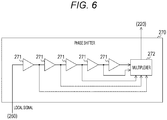
Fig. 6 is a circuit diagram showing a configuration example of thephase shifter 270 in the second embodiment of the present technology. Thephase shifter 270 includes a predetermined number of (e.g., five)delay circuits 271 and amultiplexer 272. - The
delay circuit 271 delays an input signal and outputs the input signal. The local signal from thelocal oscillator 260 is input to an input terminal of thefirst delay circuit 271. Further, an output terminal of the first delay circuit is connected to an input terminal of thesecond delay circuit 271 and themultiplexer 272. Note that the number of thedelay circuits 271 is not limited to five. - An output terminal of the second delay circuit is connected to an input terminal of the
third delay circuit 271 and themultiplexer 272. An output terminal of the third delay circuit is connected to an input terminal of thefourth delay circuit 271 and themultiplexer 272. An output terminal of the fourth delay circuit is connected to an input terminal of thefifth delay circuit 271 and themultiplexer 272. An output terminal of the fifth delay circuit is connected to themultiplexer 272. - The
multiplexer 272 selects one of the signals of therespective delay circuits 271 and supplies the selected signal to thereception circuit 220. The signal to be selected is set by a register or the like in advance before communication. - As described above, according to the second embodiment of the present technology, the
phase shifter 270 corrects the phase error of the local signal. Accordingly, verification accuracy of the loop-back test can be improved. - In the first embodiment described above, the
transmission circuit 240 and the loop-back testsignal generation circuit 230 share thelocal oscillator 260. However, in this configuration, a phase error may occur in the local signal transmitted not via the loop-back testsignal generation circuit 230, with respect to a phase of the loop-back test signal that is a signal transmitted via the circuit. Consequently, verification accuracy of the loop-back test may be reduced. The transmission/reception circuit 200 in the third embodiment is different from that in the first embodiment in that thetransmission circuit 240 and the loop-back testsignal generation circuit 230 individually include a local oscillator. -
Fig. 7 is a block diagram showing a configuration example of the transmission/reception circuit 200 in the third embodiment of the present technology. The transmission/reception circuit 200 in the third embodiment is different from that in the first embodiment in that thelocal oscillator 260 is not provided. -
Fig. 8 is circuit diagrams showing configuration examples of thetransmission circuit 240, the loop-back testsignal generation circuit 230, and thereception circuit 220 in the third embodiment of the present technology. A part "a" ofFig. 3 is a circuit diagram showing a configuration example of thetransmission circuit 240, and a part "b" ofFig. 3 is a circuit diagram showing a configuration example of the loop-back testsignal generation circuit 230. Further, a part "c" ofFig. 3 is a circuit diagram showing a configuration example of thereception circuit 220. - The
transmission circuit 240 in the third embodiment is different from that in the first embodiment in that alocal oscillator 243 is further provided. Thelocal oscillator 243 supplies a local signal to themixer 241. Note that thelocal oscillator 243 is an example of a first local oscillator recited in CLAIMS, and themixer 241 is an example of a first mixer recited in CLAIMS. - The loop-back test
signal generation circuit 230 in the third embodiment is different from that in the first embodiment in that alocal oscillator 233 is further provided. Thelocal oscillator 233 supplies a local signal to themixer 231. Note that thelocal oscillator 233 is an example of a third local oscillator recited in CLAIMS, and themixer 231 is an example of a third mixer recited in CLAIMS. - The
reception circuit 220 in the third embodiment is different from that in the first embodiment in that alocal oscillator 223 is further provided. Thelocal oscillator 223 supplies a local signal to themixer 221. Note that thelocal oscillator 223 is an example of a second local oscillator recited in CLAIMS, and themixer 221 is an example of a second mixer recited in CLAIMS. - Further, the local signals generated by the respective
local oscillators - As described above, according to the second embodiment of the present technology, the local oscillators having the same phase are provided in the
transmission circuit 240 and the loop-back testsignal generation circuit 230, respectively. With this arrangement, the phase error of the local signal can be restrained. - In the third embodiment described above, the local oscillators are individually arranged in the
transmission circuit 240, the loop-back testsignal generation circuit 230, and thereception circuit 220, respectively. However, this arrangement increases a circuit scale and costs, as compared to a configuration in which those circuits share a local oscillator. The transmission/reception circuit 200 in a fourth embodiment is different from that in the third embodiment in that the loop-back testsignal generation circuit 230 generates a loop-back test signal by using a transmission signal instead of a local signal. -
Fig. 9 is a block diagram showing a configuration example of the transmission/reception circuit 200 in the fourth embodiment of the present technology. The transmission/reception circuit 200 in the fourth embodiment is different from that in the third embodiment in that the loop-back testsignal generation circuit 230 generates a loop-back test signal by using a reception signal. -
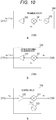
Fig. 10 is circuit diagrams showing configuration examples of thetransmission circuit 240, the loop-back testsignal generation circuit 230, and thereception circuit 220 in the fourth embodiment of the present technology. A part "a" ofFig. 3 is a circuit diagram showing a configuration example of thetransmission circuit 240, and a part "b" ofFig. 3 is a circuit diagram showing a configuration example of the loop-back testsignal generation circuit 230. Further, a part "c" ofFig. 3 is a circuit diagram showing a configuration example of thereception circuit 220. - In the
transmission circuit 240, thelocal oscillator 243 generates a local signal having a local frequency fLO1. - Further, the
local oscillator 233 is not arranged in the loop-back testsignal generation circuit 230. In the loop-back testsignal generation circuit 230, themixer 231 mixes a transmission signal having the transmission frequency fTX and a test information signal having the frequency fpr, thereby generating a local loop-back signal. - Further, in the
reception circuit 220, thelocal oscillator 223 generates a local signal having a frequency fLO2 that is the same as the transmission frequency fTX and supplies the local signal to themixer 221. - As described above, according to the fourth embodiment of the present technology, the loop-back test
signal generation circuit 230 generates a loop-back test signal by using a transmission signal instead of a local signal. Therefore, the local oscillator in the loop-back testsignal generation circuit 230 can be omitted. - In the fourth embodiment described above, the loop-back test
signal generation circuit 230 generates a loop-back test signal by using a transmission signal. However, thetransmission circuit 240 cannot be stopped during the loop-back test, which makes it difficult to reduce power consumption. The transmission/reception circuit 200 in a fifth embodiment is different from that in the fourth embodiment in that thetransmission circuit 240 and the loop-back testsignal generation circuit 230 share thelocal oscillator 260. -
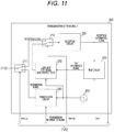
Fig. 11 is a block diagram showing a configuration example of the transmission/reception circuit 200 in the fifth embodiment of the present technology. The transmission/reception circuit 200 in the fifth embodiment is different from that in the fourth embodiment in that thelocal oscillator 260 is further provided. Thelocal oscillator 260 supplies a local signal to thetransmission circuit 240 and the loop-back testsignal generation circuit 230. Thetransmission circuit 240 modulates a transmission information signal by using the local signal, and the loop-back testsignal generation circuit 230 modulates a test information signal by using the local signal. -
Fig. 12 is circuit diagrams showing configuration examples of thetransmission circuit 240, the loop-back testsignal generation circuit 230, and thereception circuit 220 in the fifth embodiment of the present technology. A part "a" ofFig. 3 is a circuit diagram showing a configuration example of thetransmission circuit 240, and a part "b" ofFig. 3 is a circuit diagram showing a configuration example of the loop-back testsignal generation circuit 230. Further, a part "c" ofFig. 3 is a circuit diagram showing a configuration example of thereception circuit 220. - A configuration of the
transmission circuit 240 in the fifth embodiment is similar to that in the fourth embodiment. A configuration of the loop-back testsignal generation circuit 230 in the fifth embodiment is similar to that in the fourth embodiment, except that a local signal is modulated instead of a transmission signal. A configuration of thereception circuit 220 in the fifth embodiment is similar to that in the fourth embodiment. Note that a phase and frequency of a local signal generated by thelocal oscillator 223 is similar to those of the local signal generated by thelocal oscillator 260. - As described above, according to the fifth embodiment of the present technology, while the
transmission circuit 240 modulates a transmission information signal, the loop-back testsignal generation circuit 230 modulates a test information signal. Therefore, power consumption can be reduced by stopping thetransmission circuit 240 during the loop-back test. - A technology according to the present disclosure is applicable to a technology that is so-called Internet of things (IoT). IoT is a mechanism in which an IoT device 9100 that is a "thing" is connected to another
IoT device 9003, the Internet, acloud 9005, and the like and exchanges information to control each other. IoT can be used in various industries such as agriculture, houses, automobiles, manufacture, distribution, and energy. -
Fig. 13 is a diagram showing an example of a schematic configuration of anIoT system 9000 to which the technology according to the present disclosure is applicable. - An
IoT device 9001 encompasses various kinds of sensors such as a temperature sensor, a humidity sensor, an illuminance sensor, an acceleration sensor, a distance sensor, an image sensor, a gas sensor, and a motion sensor. Further, theIoT device 9001 may encompass terminals such as a smartphone, a mobile phone, a wearable terminal, and a game console. Power is supplied to theIoT device 9001 from an AC power supply, a DC power supply, a battery, non-contact power supply, so-called energy harvesting, or the like. TheIoT device 9001 can perform communication via wired, wireless, proximity wireless communication, or the like. As a communication method, 3G/LTE, WiFi, IEEE802.15.4, Bluetooth, Zigbee (registered trademark), Z-Wave, or the like is suitably used. TheIoT device 9001 may switch those plurality of communication means to perform communication. - The
IoT device 9001 may form a peer-to-peer, star, tree, or meshed network. TheIoT device 9001 may be connected to theexternal cloud 9005 directly or via agateway 9002. An address is given to theIoT device 9001 by using IPv4, IPv6, 6LoWPAN, or the like. Data collected from theIoT device 9001 is transmitted to anotherIoT device 9003, aserver 9004, thecloud 9005, or the like. A timing at which or a frequency with which data is transmitted from theIoT device 9001 may be suitably adjusted, and data may be compressed and transmitted. Such data may be used as it is, or data may be analyzed by acomputer 9008 with the use of various means such as statistical analysis, machine learning, data mining, cluster analysis, discriminant analysis, combination analysis, and time series analysis. By using such data, it is possible to provide various services such as control, warning, monitoring, visualization, automation, and optimization. - The technology according to the present disclosure are also applicable to devices and services regarding a house. The
IoT device 9001 in a house encompasses a washing machine, a drying machine, a dryer, a microwave oven, a dishwasher, a refrigerator, an oven, a rice cooker, a cooking tool, a gas appliance, a fire alarm, a thermostat, an air conditioner, a television, a recorder, audio equipment, lighting equipment, a water heater, a hot water dispenser, a vacuum cleaner, a fan, an air cleaner, a security camera, a lock, a door/shutter opening and closing apparatus, a sprinkler, a toilet, a thermometer, a weighing scale, a sphygmomanometer, and the like. TheIoT device 9001 may further encompass a solar cell, a fuel cell, a storage battery, a gas meter, an electricity meter, and a distribution board. - A communication method of the
IoT device 9001 in a house is desirably a low-power-consumption communication method. Further, theIoT device 9001 may perform communication via WiFi inside the house and via 3G/LTE outside the house. Anexternal server 9006 for controlling the IoT device may be installed in thecloud 9005 to control theIoT device 9001. TheIoT device 9001 transmits data such as a situation of a home appliance, temperature, humidity, energy consumption, and presence/absence of a person/animal inside/outside the house. Data transmitted from the home appliances is accumulated in theexternal server 9006 via thecloud 9005. A new service is provided on the basis of such data. Such anIoT device 9001 can be controlled by audio with the use of an audio recognition technology. - Further, it is possible to directly transmit information from various home appliances to a television to visualize a state of the various home appliances. Further, various sensors determine presence/absence of a resident and transmit data to an air conditioner, a light, and the like and can therefore turn on and off power supplies thereof. Furthermore, it is possible to display an advertisement on displays provided on the various home appliances via the Internet.
- Hereinabove, there have been described an example of the
IoT system 9000 to which the technology according to the present disclosure is applicable. The technology according to the present disclosure is suitably applicable to theIoT device 9001 in the configuration described above. Specifically, thecommunication apparatus 100 ofFig. 1 can be applicable to theIoT device 9001. By applying the technology according to the present disclosure to theIoT device 9001, it is possible to execute a loop-back test during wireless transmission so as to improve reliability of theIoT device 9001. - Note that the above-described embodiments are examples for embodying the present technology, and matters in the embodiments each have a corresponding relationship with disclosure-specific matters in the claims. Likewise, the matters in the embodiments of the present technology and the disclosure-specific matters in the claims denoted by the same names have a corresponding relationship with each other. However, the present technology is not limited to the embodiments, and various modifications of the embodiments may be embodied in the scope of the present technology without departing from the spirit of the present technology.
- Additionally, the present technology may also be configured as below.
- (1) A transmission/reception circuit including:
- a transmission circuit that modulates a transmission information signal and supplies the transmission information signal, as a transmission signal, to an antenna;
- a loop-back test signal generation circuit that modulates a predetermined signal to be modulated and supplies the predetermined signal to be modulated as a loop-back test signal;
- a selection unit that selects one of a reception signal from the antenna or the loop-back test signal, and supplies the selected signal as a signal to be demodulated;
- a reception circuit that demodulates the signal to be demodulated and acquires a reception information signal; and
- a test circuit that compares the reception information signal and the predetermined signal to be modulated.
- (2) The transmission/reception circuit according to (1), further including
a local oscillator that generates a predetermined local signal and supplies the predetermined local signal to the transmission circuit and the loop-back test signal generation circuit,
in which the transmission circuit mixes the predetermined local signal and the transmission information signal, and
the loop-back test signal generation circuit mixes the predetermined local signal and the predetermined signal to be modulated. - (3) The transmission/reception circuit according to (2),
in which the local oscillator further transmits the predetermined local signal to the reception circuit, and
the reception circuit mixes the predetermined local signal and the signal to be demodulated. - (4) The transmission/reception circuit according to (3), further including
a phase shifter that corrects a phase error of the predetermined local signal and supplies the predetermined local signal to the reception circuit,
in which the local oscillator supplies the predetermined local signal to the reception circuit via the phase shifter. - (5) The transmission/reception circuit according to (1),
in which the transmission circuit includes
a first local oscillator that generates a first local signal, and
a first mixer that mixes the first local signal and the transmission information signal, and
the reception circuit includes
a second local oscillator that generates a second local signal, and
a second mixer that mixes the second local signal and the signal to be demodulated. - (6) The transmission/reception circuit according to (5),
in which the loop-back test signal generation circuit includes a third local oscillator that generates a third local signal, and
a third mixer that mixes the third local signal and the predetermined signal to be modulated. - (7) The transmission/reception circuit according to (5),
in which the transmission circuit supplies the transmission signal to the antenna and supplies the transmission signal, as the predetermined signal to be modulated, to the loop-back test signal generation circuit. - (8) A communication apparatus including:
- a transmission circuit that modulates a transmission information signal and supplies the transmission information signal, as a transmission signal, to an antenna;
- the antenna that transmits the transmission signal and receives a reception signal;
- a loop-back test signal generation circuit that modulates a predetermined signal to be modulated and supplies the predetermined signal to be modulated as a loop-back test signal;
- a selection unit that selects one of the reception signal from the antenna or the loop-back test signal, and supplies the selected signal as a signal to be demodulated;
- a reception circuit that demodulates the signal to be demodulated and acquires a reception information signal; and
- a test circuit that compares the reception information signal and the predetermined signal to be modulated.
- (9) A method of controlling a transmission/reception circuit, including:
- a transmission step of modulating a transmission information signal and supplying the transmission information signal, as a transmission signal, to an antenna;
- a loop-back test signal generation step of modulating a predetermined signal to be modulated and supplying the predetermined signal to be modulated as a loop-back test signal;
- a selection step of selecting one of a reception signal from the antenna or the loop-back test signal, and supplying the selected signal as a signal to be demodulated;
- a reception step of demodulating the signal to be demodulated and acquiring a reception information signal; and
- a test step of comparing the reception information signal and the predetermined signal to be modulated.
-
- 100
- Communication apparatus
- 110
- Antenna
- 120
- Signal processing unit
- 200
- Transmission/reception circuit
- 211, 212
- Selector
- 220
- Reception circuit
- 221, 231, 241
- Mixer
- 222, 232, 242
- Low-noise amplifier
- 223, 233, 243, 260
- Local oscillator
- 230
- Loop-back test signal generation circuit
- 240
- Transmission circuit
- 250
- Test circuit
- 270
- Phase shifter
- 271
- Delay circuit
- 272
- Multiplexer
- 9001
- IoT device
Claims (9)
- A transmission/reception circuit comprising:a transmission circuit that modulates a transmission information signal and supplies the transmission information signal, as a transmission signal, to an antenna;a loop-back test signal generation circuit that modulates a predetermined signal to be modulated and supplies the predetermined signal to be modulated as a loop-back test signal;a selection unit that selects one of a reception signal from the antenna or the loop-back test signal, and supplies the selected signal as a signal to be demodulated;a reception circuit that demodulates the signal to be demodulated and acquires a reception information signal; anda test circuit that compares the reception information signal and the predetermined signal to be modulated.
- The transmission/reception circuit according to claim 1, further comprising
a local oscillator that generates a predetermined local signal and supplies the predetermined local signal to the transmission circuit and the loop-back test signal generation circuit,
wherein the transmission circuit mixes the predetermined local signal and the transmission information signal, and
the loop-back test signal generation circuit mixes the predetermined local signal and the predetermined signal to be modulated. - The transmission/reception circuit according to claim 2,
wherein the local oscillator further transmits the predetermined local signal to the reception circuit, and
the reception circuit mixes the predetermined local signal and the signal to be demodulated. - The transmission/reception circuit according to claim 3, further comprising
a phase shifter that corrects a phase error of the predetermined local signal and supplies the predetermined local signal to the reception circuit,
wherein the local oscillator supplies the predetermined local signal to the reception circuit via the phase shifter. - The transmission/reception circuit according to claim 1,
wherein the transmission circuit includes
a first local oscillator that generates a first local signal, and
a first mixer that mixes the first local signal and the transmission information signal, and
the reception circuit includes
a second local oscillator that generates a second local signal, and
a second mixer that mixes the second local signal and the signal to be demodulated. - The transmission/reception circuit according to claim 5,
wherein the loop-back test signal generation circuit includes
a third local oscillator that generates a third local signal, and
a third mixer that mixes the third local signal and the predetermined signal to be modulated. - The transmission/reception circuit according to claim 5,
wherein the transmission circuit supplies the transmission signal to the antenna and supplies the transmission signal, as the predetermined signal to be modulated, to the loop-back test signal generation circuit. - A communication apparatus comprising:a transmission circuit that modulates a transmission information signal and supplies the transmission information signal, as a transmission signal, to an antenna;the antenna that transmits the transmission signal and receives a reception signal;a loop-back test signal generation circuit that modulates a predetermined signal to be modulated and supplies the predetermined signal to be modulated as a loop-back test signal;a selection unit that selects one of the reception signal from the antenna or the loop-back test signal, and supplies the selected signal as a signal to be demodulated;a reception circuit that demodulates the signal to be demodulated and acquires a reception information signal; anda test circuit that compares the reception information signal and the predetermined signal to be modulated.
- A method of controlling a transmission/reception circuit, comprising:a transmission step of modulating a transmission information signal and supplying the transmission information signal, as a transmission signal, to an antenna;a loop-back test signal generation step of modulating a predetermined signal to be modulated and supplying the predetermined signal to be modulated as a loop-back test signal;a selection step of selecting one of a reception signal from the antenna or the loop-back test signal, and supplying the selected signal as a signal to be demodulated;a reception step of demodulating the signal to be demodulated and acquiring a reception information signal; anda test step of comparing the reception information signal and the predetermined signal to be modulated.
Applications Claiming Priority (2)
| Application Number | Priority Date | Filing Date | Title |
|---|---|---|---|
| JP2017209222 | 2017-10-30 | ||
| PCT/JP2018/029254 WO2019087501A1 (en) | 2017-10-30 | 2018-08-03 | Transmission/reception circuit, communication device, and method for controlling transmission/reception circuit |
Publications (3)
| Publication Number | Publication Date |
|---|---|
| EP3706338A1 true EP3706338A1 (en) | 2020-09-09 |
| EP3706338A4 EP3706338A4 (en) | 2020-12-23 |
| EP3706338B1 EP3706338B1 (en) | 2023-10-04 |
Family
ID=66331577
Family Applications (1)
| Application Number | Title | Priority Date | Filing Date |
|---|---|---|---|
| EP18873604.5A Active EP3706338B1 (en) | 2017-10-30 | 2018-08-03 | Transmission/reception circuit, communication device, and method for controlling transmission/reception circuit |
Country Status (5)
| Country | Link |
|---|---|
| US (1) | US10938491B2 (en) |
| EP (1) | EP3706338B1 (en) |
| JP (1) | JP7121744B2 (en) |
| CN (1) | CN111247751B (en) |
| WO (1) | WO2019087501A1 (en) |
Families Citing this family (2)
| Publication number | Priority date | Publication date | Assignee | Title |
|---|---|---|---|---|
| US11695439B2 (en) | 2020-10-30 | 2023-07-04 | Mediatek Inc. | Semiconductor chip with local oscillator buffer reused for signal transmission and associated transmission method |
| US11601147B2 (en) * | 2020-10-30 | 2023-03-07 | Mediatek Inc. | Semiconductor chip with local oscillator buffer reused for loop-back test and associated loop-back test method |
Family Cites Families (14)
| Publication number | Priority date | Publication date | Assignee | Title |
|---|---|---|---|---|
| JPH06120860A (en) | 1992-10-08 | 1994-04-28 | Oki Electric Ind Co Ltd | On-vehicle radio equipment for inter-road vehicle information system |
| JPH1065746A (en) | 1996-08-19 | 1998-03-06 | Nec Eng Ltd | Radio telephone equipment |
| US5933767A (en) * | 1997-09-15 | 1999-08-03 | Motorola, Inc. | Apparatus and method for tuning the gain of a transmitter utilizing cartesian feedback |
| US6819938B2 (en) * | 2001-06-26 | 2004-11-16 | Qualcomm Incorporated | System and method for power control calibration and a wireless communication device |
| US7464314B2 (en) * | 2005-05-12 | 2008-12-09 | Realtek Semiconductor Corp. | Method for validating an integrated circuit and related semiconductor product thereof |
| JP2009060174A (en) | 2007-08-29 | 2009-03-19 | Fujitsu Ltd | Wireless device, wireless circuit, and wireless circuit control method |
| JP4618742B2 (en) | 2008-03-11 | 2011-01-26 | Okiセミコンダクタ株式会社 | Wireless device with self-diagnosis function |
| CN101651480B (en) * | 2008-08-14 | 2013-04-24 | 华为技术有限公司 | Active antenna, base station, method for updating amplitude and phase, and signal processing method |
| JP5334318B2 (en) * | 2009-11-30 | 2013-11-06 | ルネサスエレクトロニクス株式会社 | Semiconductor integrated circuit for communication and operation method thereof |
| JP5473746B2 (en) | 2010-04-22 | 2014-04-16 | 三菱電機株式会社 | Communication device |
| US8583970B2 (en) | 2011-05-13 | 2013-11-12 | James Francis Harvey | Enhancing a receiver for improved impairment/fault detection when handling the reception of intermittent signals |
| EP2637312B1 (en) * | 2012-03-08 | 2017-01-11 | Intel Deutschland GmbH | Algorithm for fine rf transceiver dc offset calibration |
| GB2512586B (en) * | 2013-04-02 | 2015-08-12 | Broadcom Corp | Switch arrangement |
| CN107104742B (en) * | 2017-04-02 | 2020-11-10 | 上海无线通信研究中心 | Calibration method and system for parallel multi-channel wireless channel measurement |
-
2018
- 2018-08-03 JP JP2019549864A patent/JP7121744B2/en active Active
- 2018-08-03 CN CN201880068241.6A patent/CN111247751B/en active Active
- 2018-08-03 WO PCT/JP2018/029254 patent/WO2019087501A1/en not_active Ceased
- 2018-08-03 US US16/758,575 patent/US10938491B2/en active Active
- 2018-08-03 EP EP18873604.5A patent/EP3706338B1/en active Active
Also Published As
| Publication number | Publication date |
|---|---|
| EP3706338B1 (en) | 2023-10-04 |
| US10938491B2 (en) | 2021-03-02 |
| WO2019087501A1 (en) | 2019-05-09 |
| US20200351001A1 (en) | 2020-11-05 |
| CN111247751B (en) | 2022-07-05 |
| JPWO2019087501A1 (en) | 2020-11-19 |
| JP7121744B2 (en) | 2022-08-18 |
| EP3706338A4 (en) | 2020-12-23 |
| CN111247751A (en) | 2020-06-05 |
Similar Documents
| Publication | Publication Date | Title |
|---|---|---|
| US10231268B2 (en) | Associating devices and users with a local area network using network identifiers | |
| US10314088B2 (en) | Associating devices and users with a local area network using network identifiers | |
| Vivek et al. | Enabling IOT services using WIFI-ZigBee gateway for a home automation system | |
| US10772137B2 (en) | Internet of things gateway and operating method of the same | |
| US10574475B2 (en) | Household appliance with bluetooth connection and authentication | |
| US11221596B2 (en) | Hub for managing networked household appliances | |
| US20160245538A1 (en) | Smart ac controller with engery measurement capability | |
| US11825254B2 (en) | Server and method for energy resource monitoring and customer engagement | |
| US20160033945A1 (en) | Household appliance and control method therefor, and household appliance system | |
| JP2015186096A (en) | Communication system, relay device, control device, server device, control method, and information processing method | |
| US10938491B2 (en) | Transmission/reception circuit, communication apparatus, and method of controlling transmission/reception circuit | |
| JP2022173297A (en) | Device status notification control device, device status notification system, device status notification method and program | |
| US20140277591A1 (en) | Electrical Equipment and Communication Apparatus | |
| US11150685B2 (en) | Electronic apparatus and method of controlling electronic apparatus | |
| JP6811418B2 (en) | Notification system, notification content setting method, and program | |
| US20180052988A1 (en) | Information processing system, information processing method, and program | |
| US20150005909A1 (en) | Communication Device, Communication Method, and Management Device | |
| JP6785449B2 (en) | Status judgment system, status judgment method and program | |
| CN115967185B (en) | Intelligent box transformer substation measurement and control system | |
| JP2015097303A (en) | Communication device for use amount monitoring, use amount monitoring system, and use amount monitoring method | |
| RU122467U1 (en) | REMOTE SOFTWARE CABINET | |
| KR20180060743A (en) | Method for providing gateway and time synchronization service for analyzing using pattern by time | |
| WO2024062768A1 (en) | Wireless communication device, and method for controlling wireless communication device | |
| KR102137415B1 (en) | Electric apparatus and method for controlling the same | |
| TWI688304B (en) | Repeater and control system |
Legal Events
| Date | Code | Title | Description |
|---|---|---|---|
| STAA | Information on the status of an ep patent application or granted ep patent |
Free format text: STATUS: THE INTERNATIONAL PUBLICATION HAS BEEN MADE |
|
| PUAI | Public reference made under article 153(3) epc to a published international application that has entered the european phase |
Free format text: ORIGINAL CODE: 0009012 |
|
| STAA | Information on the status of an ep patent application or granted ep patent |
Free format text: STATUS: REQUEST FOR EXAMINATION WAS MADE |
|
| 17P | Request for examination filed |
Effective date: 20200506 |
|
| AK | Designated contracting states |
Kind code of ref document: A1 Designated state(s): AL AT BE BG CH CY CZ DE DK EE ES FI FR GB GR HR HU IE IS IT LI LT LU LV MC MK MT NL NO PL PT RO RS SE SI SK SM TR |
|
| AX | Request for extension of the european patent |
Extension state: BA ME |
|
| A4 | Supplementary search report drawn up and despatched |
Effective date: 20201124 |
|
| RIC1 | Information provided on ipc code assigned before grant |
Ipc: H04B 17/29 20150101AFI20201118BHEP Ipc: H04B 17/14 20150101ALI20201118BHEP |
|
| DAV | Request for validation of the european patent (deleted) | ||
| DAX | Request for extension of the european patent (deleted) | ||
| STAA | Information on the status of an ep patent application or granted ep patent |
Free format text: STATUS: EXAMINATION IS IN PROGRESS |
|
| 17Q | First examination report despatched |
Effective date: 20210722 |
|
| GRAP | Despatch of communication of intention to grant a patent |
Free format text: ORIGINAL CODE: EPIDOSNIGR1 |
|
| STAA | Information on the status of an ep patent application or granted ep patent |
Free format text: STATUS: GRANT OF PATENT IS INTENDED |
|
| INTG | Intention to grant announced |
Effective date: 20230426 |
|
| GRAS | Grant fee paid |
Free format text: ORIGINAL CODE: EPIDOSNIGR3 |
|
| GRAA | (expected) grant |
Free format text: ORIGINAL CODE: 0009210 |
|
| STAA | Information on the status of an ep patent application or granted ep patent |
Free format text: STATUS: THE PATENT HAS BEEN GRANTED |
|
| AK | Designated contracting states |
Kind code of ref document: B1 Designated state(s): AL AT BE BG CH CY CZ DE DK EE ES FI FR GB GR HR HU IE IS IT LI LT LU LV MC MK MT NL NO PL PT RO RS SE SI SK SM TR |
|
| REG | Reference to a national code |
Ref country code: GB Ref legal event code: FG4D |
|
| REG | Reference to a national code |
Ref country code: CH Ref legal event code: EP |
|
| REG | Reference to a national code |
Ref country code: DE Ref legal event code: R096 Ref document number: 602018058907 Country of ref document: DE |
|
| REG | Reference to a national code |
Ref country code: IE Ref legal event code: FG4D |
|
| REG | Reference to a national code |
Ref country code: LT Ref legal event code: MG9D |
|
| REG | Reference to a national code |
Ref country code: NL Ref legal event code: MP Effective date: 20231004 |
|
| REG | Reference to a national code |
Ref country code: AT Ref legal event code: MK05 Ref document number: 1618855 Country of ref document: AT Kind code of ref document: T Effective date: 20231004 |
|
| PG25 | Lapsed in a contracting state [announced via postgrant information from national office to epo] |
Ref country code: NL Free format text: LAPSE BECAUSE OF FAILURE TO SUBMIT A TRANSLATION OF THE DESCRIPTION OR TO PAY THE FEE WITHIN THE PRESCRIBED TIME-LIMIT Effective date: 20231004 |
|
| PG25 | Lapsed in a contracting state [announced via postgrant information from national office to epo] |
Ref country code: GR Free format text: LAPSE BECAUSE OF FAILURE TO SUBMIT A TRANSLATION OF THE DESCRIPTION OR TO PAY THE FEE WITHIN THE PRESCRIBED TIME-LIMIT Effective date: 20240105 |
|
| PG25 | Lapsed in a contracting state [announced via postgrant information from national office to epo] |
Ref country code: IS Free format text: LAPSE BECAUSE OF FAILURE TO SUBMIT A TRANSLATION OF THE DESCRIPTION OR TO PAY THE FEE WITHIN THE PRESCRIBED TIME-LIMIT Effective date: 20240204 |
|
| PG25 | Lapsed in a contracting state [announced via postgrant information from national office to epo] |
Ref country code: LT Free format text: LAPSE BECAUSE OF FAILURE TO SUBMIT A TRANSLATION OF THE DESCRIPTION OR TO PAY THE FEE WITHIN THE PRESCRIBED TIME-LIMIT Effective date: 20231004 |
|
| PG25 | Lapsed in a contracting state [announced via postgrant information from national office to epo] |
Ref country code: AT Free format text: LAPSE BECAUSE OF FAILURE TO SUBMIT A TRANSLATION OF THE DESCRIPTION OR TO PAY THE FEE WITHIN THE PRESCRIBED TIME-LIMIT Effective date: 20231004 |
|
| PG25 | Lapsed in a contracting state [announced via postgrant information from national office to epo] |
Ref country code: ES Free format text: LAPSE BECAUSE OF FAILURE TO SUBMIT A TRANSLATION OF THE DESCRIPTION OR TO PAY THE FEE WITHIN THE PRESCRIBED TIME-LIMIT Effective date: 20231004 |
|
| PG25 | Lapsed in a contracting state [announced via postgrant information from national office to epo] |
Ref country code: LT Free format text: LAPSE BECAUSE OF FAILURE TO SUBMIT A TRANSLATION OF THE DESCRIPTION OR TO PAY THE FEE WITHIN THE PRESCRIBED TIME-LIMIT Effective date: 20231004 Ref country code: IS Free format text: LAPSE BECAUSE OF FAILURE TO SUBMIT A TRANSLATION OF THE DESCRIPTION OR TO PAY THE FEE WITHIN THE PRESCRIBED TIME-LIMIT Effective date: 20240204 Ref country code: GR Free format text: LAPSE BECAUSE OF FAILURE TO SUBMIT A TRANSLATION OF THE DESCRIPTION OR TO PAY THE FEE WITHIN THE PRESCRIBED TIME-LIMIT Effective date: 20240105 Ref country code: ES Free format text: LAPSE BECAUSE OF FAILURE TO SUBMIT A TRANSLATION OF THE DESCRIPTION OR TO PAY THE FEE WITHIN THE PRESCRIBED TIME-LIMIT Effective date: 20231004 Ref country code: BG Free format text: LAPSE BECAUSE OF FAILURE TO SUBMIT A TRANSLATION OF THE DESCRIPTION OR TO PAY THE FEE WITHIN THE PRESCRIBED TIME-LIMIT Effective date: 20240104 Ref country code: AT Free format text: LAPSE BECAUSE OF FAILURE TO SUBMIT A TRANSLATION OF THE DESCRIPTION OR TO PAY THE FEE WITHIN THE PRESCRIBED TIME-LIMIT Effective date: 20231004 Ref country code: PT Free format text: LAPSE BECAUSE OF FAILURE TO SUBMIT A TRANSLATION OF THE DESCRIPTION OR TO PAY THE FEE WITHIN THE PRESCRIBED TIME-LIMIT Effective date: 20240205 |
|
| P01 | Opt-out of the competence of the unified patent court (upc) registered |
Effective date: 20240329 |
|
| PG25 | Lapsed in a contracting state [announced via postgrant information from national office to epo] |
Ref country code: SE Free format text: LAPSE BECAUSE OF FAILURE TO SUBMIT A TRANSLATION OF THE DESCRIPTION OR TO PAY THE FEE WITHIN THE PRESCRIBED TIME-LIMIT Effective date: 20231004 Ref country code: RS Free format text: LAPSE BECAUSE OF FAILURE TO SUBMIT A TRANSLATION OF THE DESCRIPTION OR TO PAY THE FEE WITHIN THE PRESCRIBED TIME-LIMIT Effective date: 20231004 Ref country code: PL Free format text: LAPSE BECAUSE OF FAILURE TO SUBMIT A TRANSLATION OF THE DESCRIPTION OR TO PAY THE FEE WITHIN THE PRESCRIBED TIME-LIMIT Effective date: 20231004 Ref country code: NO Free format text: LAPSE BECAUSE OF FAILURE TO SUBMIT A TRANSLATION OF THE DESCRIPTION OR TO PAY THE FEE WITHIN THE PRESCRIBED TIME-LIMIT Effective date: 20240104 Ref country code: LV Free format text: LAPSE BECAUSE OF FAILURE TO SUBMIT A TRANSLATION OF THE DESCRIPTION OR TO PAY THE FEE WITHIN THE PRESCRIBED TIME-LIMIT Effective date: 20231004 Ref country code: HR Free format text: LAPSE BECAUSE OF FAILURE TO SUBMIT A TRANSLATION OF THE DESCRIPTION OR TO PAY THE FEE WITHIN THE PRESCRIBED TIME-LIMIT Effective date: 20231004 |
|
| REG | Reference to a national code |
Ref country code: DE Ref legal event code: R097 Ref document number: 602018058907 Country of ref document: DE |
|
| PG25 | Lapsed in a contracting state [announced via postgrant information from national office to epo] |
Ref country code: DK Free format text: LAPSE BECAUSE OF FAILURE TO SUBMIT A TRANSLATION OF THE DESCRIPTION OR TO PAY THE FEE WITHIN THE PRESCRIBED TIME-LIMIT Effective date: 20231004 |
|
| PG25 | Lapsed in a contracting state [announced via postgrant information from national office to epo] |
Ref country code: CZ Free format text: LAPSE BECAUSE OF FAILURE TO SUBMIT A TRANSLATION OF THE DESCRIPTION OR TO PAY THE FEE WITHIN THE PRESCRIBED TIME-LIMIT Effective date: 20231004 |
|
| PG25 | Lapsed in a contracting state [announced via postgrant information from national office to epo] |
Ref country code: SK Free format text: LAPSE BECAUSE OF FAILURE TO SUBMIT A TRANSLATION OF THE DESCRIPTION OR TO PAY THE FEE WITHIN THE PRESCRIBED TIME-LIMIT Effective date: 20231004 |
|
| PG25 | Lapsed in a contracting state [announced via postgrant information from national office to epo] |
Ref country code: SM Free format text: LAPSE BECAUSE OF FAILURE TO SUBMIT A TRANSLATION OF THE DESCRIPTION OR TO PAY THE FEE WITHIN THE PRESCRIBED TIME-LIMIT Effective date: 20231004 Ref country code: SK Free format text: LAPSE BECAUSE OF FAILURE TO SUBMIT A TRANSLATION OF THE DESCRIPTION OR TO PAY THE FEE WITHIN THE PRESCRIBED TIME-LIMIT Effective date: 20231004 Ref country code: RO Free format text: LAPSE BECAUSE OF FAILURE TO SUBMIT A TRANSLATION OF THE DESCRIPTION OR TO PAY THE FEE WITHIN THE PRESCRIBED TIME-LIMIT Effective date: 20231004 Ref country code: IT Free format text: LAPSE BECAUSE OF FAILURE TO SUBMIT A TRANSLATION OF THE DESCRIPTION OR TO PAY THE FEE WITHIN THE PRESCRIBED TIME-LIMIT Effective date: 20231004 Ref country code: EE Free format text: LAPSE BECAUSE OF FAILURE TO SUBMIT A TRANSLATION OF THE DESCRIPTION OR TO PAY THE FEE WITHIN THE PRESCRIBED TIME-LIMIT Effective date: 20231004 Ref country code: DK Free format text: LAPSE BECAUSE OF FAILURE TO SUBMIT A TRANSLATION OF THE DESCRIPTION OR TO PAY THE FEE WITHIN THE PRESCRIBED TIME-LIMIT Effective date: 20231004 Ref country code: CZ Free format text: LAPSE BECAUSE OF FAILURE TO SUBMIT A TRANSLATION OF THE DESCRIPTION OR TO PAY THE FEE WITHIN THE PRESCRIBED TIME-LIMIT Effective date: 20231004 |
|
| PLBE | No opposition filed within time limit |
Free format text: ORIGINAL CODE: 0009261 |
|
| STAA | Information on the status of an ep patent application or granted ep patent |
Free format text: STATUS: NO OPPOSITION FILED WITHIN TIME LIMIT |
|
| 26N | No opposition filed |
Effective date: 20240705 |
|
| PGFP | Annual fee paid to national office [announced via postgrant information from national office to epo] |
Ref country code: GB Payment date: 20240723 Year of fee payment: 7 |
|
| PG25 | Lapsed in a contracting state [announced via postgrant information from national office to epo] |
Ref country code: SI Free format text: LAPSE BECAUSE OF FAILURE TO SUBMIT A TRANSLATION OF THE DESCRIPTION OR TO PAY THE FEE WITHIN THE PRESCRIBED TIME-LIMIT Effective date: 20231004 |
|
| PG25 | Lapsed in a contracting state [announced via postgrant information from national office to epo] |
Ref country code: SI Free format text: LAPSE BECAUSE OF FAILURE TO SUBMIT A TRANSLATION OF THE DESCRIPTION OR TO PAY THE FEE WITHIN THE PRESCRIBED TIME-LIMIT Effective date: 20231004 |
|
| REG | Reference to a national code |
Ref country code: CH Ref legal event code: PL |
|
| PG25 | Lapsed in a contracting state [announced via postgrant information from national office to epo] |
Ref country code: LU Free format text: LAPSE BECAUSE OF NON-PAYMENT OF DUE FEES Effective date: 20240803 |
|
| PG25 | Lapsed in a contracting state [announced via postgrant information from national office to epo] |
Ref country code: MC Free format text: LAPSE BECAUSE OF FAILURE TO SUBMIT A TRANSLATION OF THE DESCRIPTION OR TO PAY THE FEE WITHIN THE PRESCRIBED TIME-LIMIT Effective date: 20231004 Ref country code: CH Free format text: LAPSE BECAUSE OF NON-PAYMENT OF DUE FEES Effective date: 20240831 |
|
| REG | Reference to a national code |
Ref country code: BE Ref legal event code: MM Effective date: 20240831 |
|
| PG25 | Lapsed in a contracting state [announced via postgrant information from national office to epo] |
Ref country code: BE Free format text: LAPSE BECAUSE OF NON-PAYMENT OF DUE FEES Effective date: 20240831 |
|
| PG25 | Lapsed in a contracting state [announced via postgrant information from national office to epo] |
Ref country code: FR Free format text: LAPSE BECAUSE OF NON-PAYMENT OF DUE FEES Effective date: 20240831 |
|
| PG25 | Lapsed in a contracting state [announced via postgrant information from national office to epo] |
Ref country code: IE Free format text: LAPSE BECAUSE OF NON-PAYMENT OF DUE FEES Effective date: 20240803 |
|
| PG25 | Lapsed in a contracting state [announced via postgrant information from national office to epo] |
Ref country code: FI Free format text: LAPSE BECAUSE OF FAILURE TO SUBMIT A TRANSLATION OF THE DESCRIPTION OR TO PAY THE FEE WITHIN THE PRESCRIBED TIME-LIMIT Effective date: 20231004 |
|
| PGFP | Annual fee paid to national office [announced via postgrant information from national office to epo] |
Ref country code: DE Payment date: 20250724 Year of fee payment: 8 |
|
| PG25 | Lapsed in a contracting state [announced via postgrant information from national office to epo] |
Ref country code: CY Free format text: LAPSE BECAUSE OF FAILURE TO SUBMIT A TRANSLATION OF THE DESCRIPTION OR TO PAY THE FEE WITHIN THE PRESCRIBED TIME-LIMIT; INVALID AB INITIO Effective date: 20180803 |
|
| PG25 | Lapsed in a contracting state [announced via postgrant information from national office to epo] |
Ref country code: HU Free format text: LAPSE BECAUSE OF FAILURE TO SUBMIT A TRANSLATION OF THE DESCRIPTION OR TO PAY THE FEE WITHIN THE PRESCRIBED TIME-LIMIT; INVALID AB INITIO Effective date: 20180803 |
|
| GBPC | Gb: european patent ceased through non-payment of renewal fee |
Effective date: 20250803 |