EP3706251A1 - Expandable connector assembly - Google Patents
Expandable connector assembly Download PDFInfo
- Publication number
- EP3706251A1 EP3706251A1 EP19826291.7A EP19826291A EP3706251A1 EP 3706251 A1 EP3706251 A1 EP 3706251A1 EP 19826291 A EP19826291 A EP 19826291A EP 3706251 A1 EP3706251 A1 EP 3706251A1
- Authority
- EP
- European Patent Office
- Prior art keywords
- connector
- female
- male
- female connectors
- female connector
- Prior art date
- Legal status (The legal status is an assumption and is not a legal conclusion. Google has not performed a legal analysis and makes no representation as to the accuracy of the status listed.)
- Granted
Links
Images




Classifications
-
- H—ELECTRICITY
- H01—ELECTRIC ELEMENTS
- H01R—ELECTRICALLY-CONDUCTIVE CONNECTIONS; STRUCTURAL ASSOCIATIONS OF A PLURALITY OF MUTUALLY-INSULATED ELECTRICAL CONNECTING ELEMENTS; COUPLING DEVICES; CURRENT COLLECTORS
- H01R12/00—Structural associations of a plurality of mutually-insulated electrical connecting elements, specially adapted for printed circuits, e.g. printed circuit boards [PCB], flat or ribbon cables, or like generally planar structures, e.g. terminal strips, terminal blocks; Coupling devices specially adapted for printed circuits, flat or ribbon cables, or like generally planar structures; Terminals specially adapted for contact with, or insertion into, printed circuits, flat or ribbon cables, or like generally planar structures
- H01R12/70—Coupling devices
- H01R12/71—Coupling devices for rigid printing circuits or like structures
- H01R12/72—Coupling devices for rigid printing circuits or like structures coupling with the edge of the rigid printed circuits or like structures
- H01R12/722—Coupling devices for rigid printing circuits or like structures coupling with the edge of the rigid printed circuits or like structures coupling devices mounted on the edge of the printed circuits
- H01R12/724—Coupling devices for rigid printing circuits or like structures coupling with the edge of the rigid printed circuits or like structures coupling devices mounted on the edge of the printed circuits containing contact members forming a right angle
-
- H—ELECTRICITY
- H01—ELECTRIC ELEMENTS
- H01R—ELECTRICALLY-CONDUCTIVE CONNECTIONS; STRUCTURAL ASSOCIATIONS OF A PLURALITY OF MUTUALLY-INSULATED ELECTRICAL CONNECTING ELEMENTS; COUPLING DEVICES; CURRENT COLLECTORS
- H01R13/00—Details of coupling devices of the kinds covered by groups H01R12/70 or H01R24/00 - H01R33/00
- H01R13/46—Bases; Cases
- H01R13/514—Bases; Cases composed as a modular blocks or assembly, i.e. composed of co-operating parts provided with contact members or holding contact members between them
-
- H—ELECTRICITY
- H01—ELECTRIC ELEMENTS
- H01R—ELECTRICALLY-CONDUCTIVE CONNECTIONS; STRUCTURAL ASSOCIATIONS OF A PLURALITY OF MUTUALLY-INSULATED ELECTRICAL CONNECTING ELEMENTS; COUPLING DEVICES; CURRENT COLLECTORS
- H01R12/00—Structural associations of a plurality of mutually-insulated electrical connecting elements, specially adapted for printed circuits, e.g. printed circuit boards [PCB], flat or ribbon cables, or like generally planar structures, e.g. terminal strips, terminal blocks; Coupling devices specially adapted for printed circuits, flat or ribbon cables, or like generally planar structures; Terminals specially adapted for contact with, or insertion into, printed circuits, flat or ribbon cables, or like generally planar structures
- H01R12/70—Coupling devices
- H01R12/77—Coupling devices for flexible printed circuits, flat or ribbon cables or like structures
- H01R12/79—Coupling devices for flexible printed circuits, flat or ribbon cables or like structures connecting to rigid printed circuits or like structures
-
- H—ELECTRICITY
- H01—ELECTRIC ELEMENTS
- H01R—ELECTRICALLY-CONDUCTIVE CONNECTIONS; STRUCTURAL ASSOCIATIONS OF A PLURALITY OF MUTUALLY-INSULATED ELECTRICAL CONNECTING ELEMENTS; COUPLING DEVICES; CURRENT COLLECTORS
- H01R13/00—Details of coupling devices of the kinds covered by groups H01R12/70 or H01R24/00 - H01R33/00
- H01R13/02—Contact members
- H01R13/04—Pins or blades for co-operation with sockets
-
- H—ELECTRICITY
- H01—ELECTRIC ELEMENTS
- H01R—ELECTRICALLY-CONDUCTIVE CONNECTIONS; STRUCTURAL ASSOCIATIONS OF A PLURALITY OF MUTUALLY-INSULATED ELECTRICAL CONNECTING ELEMENTS; COUPLING DEVICES; CURRENT COLLECTORS
- H01R13/00—Details of coupling devices of the kinds covered by groups H01R12/70 or H01R24/00 - H01R33/00
- H01R13/02—Contact members
- H01R13/10—Sockets for co-operation with pins or blades
-
- H—ELECTRICITY
- H01—ELECTRIC ELEMENTS
- H01R—ELECTRICALLY-CONDUCTIVE CONNECTIONS; STRUCTURAL ASSOCIATIONS OF A PLURALITY OF MUTUALLY-INSULATED ELECTRICAL CONNECTING ELEMENTS; COUPLING DEVICES; CURRENT COLLECTORS
- H01R13/00—Details of coupling devices of the kinds covered by groups H01R12/70 or H01R24/00 - H01R33/00
- H01R13/62—Means for facilitating engagement or disengagement of coupling parts or for holding them in engagement
- H01R13/627—Snap or like fastening
-
- H—ELECTRICITY
- H01—ELECTRIC ELEMENTS
- H01R—ELECTRICALLY-CONDUCTIVE CONNECTIONS; STRUCTURAL ASSOCIATIONS OF A PLURALITY OF MUTUALLY-INSULATED ELECTRICAL CONNECTING ELEMENTS; COUPLING DEVICES; CURRENT COLLECTORS
- H01R13/00—Details of coupling devices of the kinds covered by groups H01R12/70 or H01R24/00 - H01R33/00
- H01R13/62—Means for facilitating engagement or disengagement of coupling parts or for holding them in engagement
- H01R13/627—Snap or like fastening
- H01R13/6271—Latching means integral with the housing
- H01R13/6273—Latching means integral with the housing comprising two latching arms
-
- H—ELECTRICITY
- H01—ELECTRIC ELEMENTS
- H01R—ELECTRICALLY-CONDUCTIVE CONNECTIONS; STRUCTURAL ASSOCIATIONS OF A PLURALITY OF MUTUALLY-INSULATED ELECTRICAL CONNECTING ELEMENTS; COUPLING DEVICES; CURRENT COLLECTORS
- H01R12/00—Structural associations of a plurality of mutually-insulated electrical connecting elements, specially adapted for printed circuits, e.g. printed circuit boards [PCB], flat or ribbon cables, or like generally planar structures, e.g. terminal strips, terminal blocks; Coupling devices specially adapted for printed circuits, flat or ribbon cables, or like generally planar structures; Terminals specially adapted for contact with, or insertion into, printed circuits, flat or ribbon cables, or like generally planar structures
- H01R12/70—Coupling devices
- H01R12/71—Coupling devices for rigid printing circuits or like structures
- H01R12/72—Coupling devices for rigid printing circuits or like structures coupling with the edge of the rigid printed circuits or like structures
- H01R12/722—Coupling devices for rigid printing circuits or like structures coupling with the edge of the rigid printed circuits or like structures coupling devices mounted on the edge of the printed circuits
Definitions
- the present disclosure relates to a connector, and more particularly, to an expandable connector assembly capable of increasing the number of pins of the connector by assembling unit male and female connectors, when it is needed to increase the number of pins of the connector.
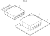
- a conventional connector generally includes a female connector 2 and a male connector 3 in a pair.
- the female connector 1 has a plurality of pins corresponding to a contact
- the male connector 3 has a plurality of plug terminals that come into contact with the plurality of pins.
- the female connector 2 is mounted to the circuit board 1 by means of SMT (Surface Mounter Technology), and the male connector 3 is connected and fixed in the female connector 2.
- the number of pins is predetermined, and the number of pins determines compatibility with a usable device or circuit board. In other words, if the number of pins is not identical between any connector and a circuit board, the connector is not useable. In this case, it is required to use male and female connectors with exactly the same number of pins or newly fabricate male and female connectors with the required number of pins.
- the number of pins must be increased by one to the male and female connectors.
- the male and female connectors must be replaced entirely.
- the present disclosure is directed to improving compatibility and economic efficiency of male and female connectors by implementing the male and female connectors in an expandable manner, where several unit connectors may be consecutively assembled when it is required to increase the number of pins of the connector.
- the present disclosure is directed to providing a connector assembly which may be prevented from being detached or disconnected due to external shocks or vibrations and also allow male and female connectors to be conveniently assembled and disassembled.
- a connector assembly comprising: a plurality of female connectors respectively having a predetermined number of pins; and at least one male connector having a plug terminal contacting the pin and coupled with the plurality of female connectors, wherein the plurality of female connectors are provided to be assembled with each other along one direction.
- Each of the plurality of female connectors may have one pin, and the at least one male connector may be respectively connected to the plurality of female connectors in one-to-one relationship.
- the at least one male connector may be a single male connector integrally having plug terminals corresponding to the total number of pins of the plurality of female connectors and be connected to the plurality of female connectors in multi-to-one relationship.
- the female connector may have a hooking protrusion bent in a vertical direction on at least one of an upper end and a lower end of a front surface thereof to which the male connector is connected, and the male connector may have a hooking groove provided to be hooked with the hooking protrusion.
- the hooking protrusion of any one female connector and the hooking protrusion of another neighboring female connector may be connected along one direction.
- the female connector may have a locking groove formed by depressing an inner surface on at least one of an upper end and a lower end of a front surface thereof to which the male connector is connected, and the male connector may have a locking pin provided at an upper end or a lower end thereof to be locked to or unlocked from the locking groove by means of a seesawing structure.
- the female connector may have a convex block formed at one side surface thereof to protrude in the one direction and a concave groove formed at the other side surface thereof to depress corresponding to the convex block, and any one female connector and another female connector may be connected to each other by vertically fitting the convex block into the concave groove.
- the convex block may have a cross-section of a "T" shape, and the concave groove is formed to engage with the convex block.
- the female connector may include a first uneven portion formed at one side surface thereof to have ridges and valleys repeatedly; and a second uneven portion formed at the other side surface thereof and shaped to engage with the first uneven portion, wherein any one female connector and another female connector may be connected to each other by vertically fitting the first uneven portion into the second uneven portion.
- the first uneven portion may be provided to have a saw-tooth form inclined in one direction.
- a circuit board may refer to a BMS (Battery Management System) circuit board applied to a battery pack for a vehicle.
- the BMS circuit board is a component of the battery pack for controlling charge/discharge and cell balancing of battery cells.
- a connector assembly according to the present disclosure may be connected to the BMS circuit board to transmit voltage information or the like of the battery cells to the BMS.
- the connector assembly of the present disclosure may be connected to a printed circuit board of an electronic device such as a laptop, a tablet PC, a smart phone, or the like, in addition to the BMS circuit board, to transmit a signal necessary for the electronic device.
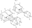
- FIG. 2 is a schematic perspective view showing unit male and female connectors according to an embodiment of the present disclosure
- FIG. 3 is a schematic perspective view showing male and female connectors, which are configured by assembling the unit male and female connectors of FIG. 2
- FIG. 4 is a schematic top view showing the female connectors of this embodiment, which are installed to a circuit board.
- the connector assembly includes a plurality of female connectors 10 provided to be assembled with each other along one direction, and an at least one male connector 20 coupled to the female connectors 10.
- each of the female connectors 10 accommodates a predetermined number of pins 11 therein.
- the female connector 10 according to this embodiment is illustrated as accommodating one pin 11, the female connector 10 may accommodate two or more pins 11.
- the plurality of female connectors 10 respectively having one pin 11 may be connected successively in one direction as shown in FIGS. 3 and 4 . If the unit female connectors 10 are successively assembled as above, it is possible to configure a female connector 10 having various numbers of pins 11. In other words, if it is necessary to decrease or increase the number of pins 11 of the female connector 10 to be connected to a circuit board 30, in the conventional art, the female connector itself must be replaced. However, according to the present disclosure, the number of pins 11 of the female connector 10 can be increased or decreased just by separating or adding one unit female connector 10. Thus, the cost of replacing the female connector may be reduced and the labor required for mounting the female connector to the circuit board may be reduced.
- the assembling structure and method of the plurality of female connectors 10 may be implemented as follows.
- the unit female connector 10 includes a convex block 15 formed at one side thereof to protrude therefrom and a concave groove 16 formed at the other side thereof to be depressed in a shape corresponding to the convex block 15.
- the convex block 15 has a cross-section of an approximately alphabetical "T" shape and extends along the height direction. Also, the concave groove 16 forms an empty space that engages with the convex block.
- Any one unit female connector 10 and another female connector 10 may be connected to each other by fitting the convex block 15 and the concave groove 16 vertically.
- two unit female connectors 10 may be connected into one body by fitting the convex block 15 of any one unit female connector 10 into the concave grooves 16 of another female connector 10 the from top to bottom.
- the two unit female connectors 10 engage with each other by means of the convex block 15 and the concave groove 16 having a "T" shape, the two unit female connectors 10 may be tightly fastened with each other without relatively moving in the forward, backward, left and right directions.
- the convex block 15 and the concave groove 16 are formed in the "T" shape in this embodiment, the convex block 15 and the concave groove 16 may have any shape such as an "L” shape as long as the convex block 15 convexly formed at one side surface of the unit female connector 10 and the concave groove 16 concavely formed at the other side surface of the unit female connector 10 are capable of engaging with each other.
- other unit female connectors 10 may be assembled and connected to the two unit female connectors 10 such that a plurality of female connectors 10 having a required number of pins 11 are connected.
- the male connector 20 may include a plurality of unit male connectors 20 that are connected to the unit female connectors 10 in one-to-one relationship.
- the unit male connector 20 is implemented to have only one plug terminal 21 that contacts one pin 11 of the female connector 10.
- FIGS. 5 and 6 are diagrams for illustrating a fastening structure between the male and female connectors 20 of this embodiment.
- the female connector 10 has hooking protrusions 12, 13 bent in a vertical direction on at least one of an upper end and a lower end of a front surface thereof to which the male connector 20 is connected. Also, the male connector 20 has hooking grooves 22, 23 provided to be hooked to the hooking protrusions 12, 13.
- the hooking protrusions 12, 13 are provided to both the upper end and the lower end of the front surface of the female connector 10 for enhanced coupling, and the hooking grooves 22, 23 corresponding thereto are provided to the upper end and the lower end of the front surface of the male connector 20.
- the male connector 20 In order to separate the male connector 20 from the female connector 10, in a state where the hooking protrusions 12, 13 of the female connector 10 are slightly widened, the male connector 20 should be pulled in the reverse direction. Although not shown in detail, the plug terminal 21 of the male connector 20 may be inserted in a receptacle manner to contact the pin 11 of the female connector 10, which is located inside the female connector 10.
- FIG. 7 is a diagram corresponding to FIG. 2 and showing a modified example of the male connector 20.
- the male connector 20 according to this embodiment is provided in a single number.
- the male connector 20 according to the modified example integrally includes plug terminals 21 corresponding to the total number of pins 11 of the plurality of unit female connectors 10 and is connected to the female connectors 10, which are assembled with each other on the circuit board 30, in a multi-to-one structure.
- the female connectors 10 assembled with each other have a front end opened in the lateral direction, and the hooking protrusions 12, 13 of any one female connector 10 and the hooking protrusions 12, 13 of another neighboring female connector 10 are connected along the assembling direction.
- the hooking grooves 22, 23 of the male connector 20 may be formed in a size corresponding to the connected hooking protrusions 12, 13.
- the hooking grooves 22, 23 of the male connector 20 may be hooked to all of the hooking protrusions 12, 13 of the female connectors 10.
- the male connector 20 also serves to bind a plurality of wires W into a bundle, it is advantageous to integrate the male connector 20 into one connector rather than dividing into several connectors. Also, since the male connector 20 is not mounted to the circuit board 30, the male connector 20 may be exchanged more easily than the female connector 10. For this reason, the connector assembly according to the modified example may be more effective than the connector assembly having the one-to-one connection structure of the male and female connectors 20 described above.
- FIGS. 8 to 10 Next, a connector assembly according to another embodiment of the present disclosure will be described with reference to FIGS. 8 to 10 .
- FIGS. 8 and 9 are diagrams for illustrating a fastening structure between male and female connectors 20 according to another embodiment of the present disclosure.
- the female connector 10 according to another embodiment of the present disclosure has a locking groove 17 formed by depressing an inner surface of at least one of an upper end and a lower end of a front surface thereof to which the male connector 20 is connected.
- the male connector 20 has a locking pin 24 provided at an upper end or a lower end thereof to be locked to or unlocked from the locking groove 17 by means of a seesawing structure.
- the locking pin 24 may be integrally formed at an outer side of a housing of the male connector 20 such that, if one end thereof based on a support point located at one site is pressed, the other end is lifted.
- the other end of the locking pin 24 may be provided with a projection 24a that at least partially engages with the locking groove 17 of the female connector 10.
- the fastening structure between the male and female connectors 20 may the male and female connectors 20 from being broken or deformed when the male connector 20 is inserted into or separated from the female connector 10.
- the hooking protrusions 12, 13 of the female connector 10 should be widened so that the male connector 20 may pass into and out of the front end of the female connector 10.
- the female connector 10 is made of a material elastically deformable within a certain range, when the female and female connectors 20 are repeatedly fastened, the coupling force of the female connector 10 is weakened due to deformation or breakage thereof.
- the male connector 20 when the male connector 20 is inserted into or separated from the female connector 10, the male connector 20 may be inserted or separated by appropriately using the locking pin 24 without widening the front end of the female connector 10.
- the male connector 20 may be inserted into or separated from the female connector 10 in a state of pressing a front portion of the locking pin 24.
- the male connector 20 may also be inserted into or separated from the female connector 10 in a state of slightly lifting up a rear portion of the locking pin 24 with a predetermined tool.
- the locking pin 24 according to this embodiment is used, there is no need to widen the front end of the female connector 10 or forcibly press the front end of the male connector 20 into the front end of the female connector 10.
- the male and female connectors 20 are fastened or released, it is possible to minimize the damage of the male and female connectors 20, thereby improving the coupling force and durability of the male and female connectors 20.
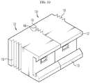
- FIGS. 10 and 11 are diagrams for illustrating an assembling structure of a plurality of female connectors 10 according to still another embodiment of the present disclosure.
- the female connector 10 includes a first uneven portion 18 formed at one side surface thereof and having ridges and valleys repeatedly and a second uneven portion 19 formed at the other side surface thereof to engage with the first uneven portion 18.
- Any one female connector 10 and another female connector 10 may be connected to each other by fitting the first uneven portion 18 vertically into the second uneven portion 19.
- the first uneven portion 18 and the second uneven portion 19 according to this embodiment may correspond to the convex block 15 and the concave groove 16 of the former embodiment.
- first uneven portion 18 and the second uneven portion 19 may easily adjust the number and depth of ridges and valleys at both side surfaces of the female connector 10, compared to the convex block 15 and the concave groove 16 of the former embodiment having a "T" shape.
- the unit female connector 10 of this embodiment may be manufactured into a slim design more easily than the female connector 10 of the former embodiment.
- the unit female connector 10 having one pin 11 should be made as slim as possible so that the entire female connector 10 formed by connecting unit female connectors may have a compact design.
- the assembling structure of the female connectors 10 according to this embodiment may be more advantageous in slimming the unit female connector 10 and the entire female connector 10 formed by connecting unit female connectors, compared to the former embodiment.
- the +X-axis direction of FIG. 11 is a direction in which the pin 11 of the female connector 10 is electrically connected to a conductive pattern of the circuit board 30 when the female connector 10 is mounted to the circuit board 30. If vibration or an external force is applied, the female connectors 10 may be pushed in the +X-axis direction, which may cut the electrical connection between the pin 11 of the female connector 10 and the conductive pattern of the circuit board 30. Thus, it is particularly needed to fix the female connector 10 to the circuit board 30 such that the female connector 10 is not pushed in the +X axis direction.
- first uneven portion 18 and the second uneven portion 19 may be provided to have a saw-tooth form inclined in one direction as shown in FIG. 11 .
Landscapes
- Details Of Connecting Devices For Male And Female Coupling (AREA)
- Coupling Device And Connection With Printed Circuit (AREA)
- Connector Housings Or Holding Contact Members (AREA)
Abstract
Description
- The present disclosure relates to a connector, and more particularly, to an expandable connector assembly capable of increasing the number of pins of the connector by assembling unit male and female connectors, when it is needed to increase the number of pins of the connector.
- The present application claims priority to Korean Patent Application No.
10-2018-0075765 filed on June 29, 2018 - As shown in
FIG. 1 , a conventional connector generally includes afemale connector 2 and amale connector 3 in a pair. The female connector 1 has a plurality of pins corresponding to a contact, and themale connector 3 has a plurality of plug terminals that come into contact with the plurality of pins. Thefemale connector 2 is mounted to the circuit board 1 by means of SMT (Surface Mounter Technology), and themale connector 3 is connected and fixed in thefemale connector 2. - However, if both the
female connector 2 and themale connector 3 are used, different bodies and contacts of thefemale connector 2 and themale connector 3 should be prepared using different molds, and any one connector must be surface-mounted to a circuit board, which makes the manufacturing process complicated and increases the manufacturing cost. - In addition, in the conventional male and female connectors, the number of pins is predetermined, and the number of pins determines compatibility with a usable device or circuit board. In other words, if the number of pins is not identical between any connector and a circuit board, the connector is not useable. In this case, it is required to use male and female connectors with exactly the same number of pins or newly fabricate male and female connectors with the required number of pins.
- In particular, in order to transmit one more signal to an existing device or circuit board, the number of pins must be increased by one to the male and female connectors. In this case, due to the structure of the existing connectors the male and female connectors must be replaced entirely.
- Thus, there is a demand for a new type connector, which allows a connector pin to be easily added without replacing the existing male and female connectors.
- The present disclosure is directed to improving compatibility and economic efficiency of male and female connectors by implementing the male and female connectors in an expandable manner, where several unit connectors may be consecutively assembled when it is required to increase the number of pins of the connector.
- In addition, the present disclosure is directed to providing a connector assembly which may be prevented from being detached or disconnected due to external shocks or vibrations and also allow male and female connectors to be conveniently assembled and disassembled.
- In one aspect of the present disclosure, there is provided a connector assembly, comprising: a plurality of female connectors respectively having a predetermined number of pins; and at least one male connector having a plug terminal contacting the pin and coupled with the plurality of female connectors, wherein the plurality of female connectors are provided to be assembled with each other along one direction.
- Each of the plurality of female connectors may have one pin, and the at least one male connector may be respectively connected to the plurality of female connectors in one-to-one relationship.
- The at least one male connector may be a single male connector integrally having plug terminals corresponding to the total number of pins of the plurality of female connectors and be connected to the plurality of female connectors in multi-to-one relationship.
- The female connector may have a hooking protrusion bent in a vertical direction on at least one of an upper end and a lower end of a front surface thereof to which the male connector is connected, and the male connector may have a hooking groove provided to be hooked with the hooking protrusion.
- When the female connectors are assembled in one direction, the hooking protrusion of any one female connector and the hooking protrusion of another neighboring female connector may be connected along one direction.
- The female connector may have a locking groove formed by depressing an inner surface on at least one of an upper end and a lower end of a front surface thereof to which the male connector is connected, and the male connector may have a locking pin provided at an upper end or a lower end thereof to be locked to or unlocked from the locking groove by means of a seesawing structure.
- The female connector may have a convex block formed at one side surface thereof to protrude in the one direction and a concave groove formed at the other side surface thereof to depress corresponding to the convex block, and any one female connector and another female connector may be connected to each other by vertically fitting the convex block into the concave groove.
- The convex block may have a cross-section of a "T" shape, and the concave groove is formed to engage with the convex block.
- The female connector may include a first uneven portion formed at one side surface thereof to have ridges and valleys repeatedly; and a second uneven portion formed at the other side surface thereof and shaped to engage with the first uneven portion, wherein any one female connector and another female connector may be connected to each other by vertically fitting the first uneven portion into the second uneven portion.
- The first uneven portion may be provided to have a saw-tooth form inclined in one direction.
- According to an embodiment of the present disclosure, when it is necessary to increase the number of pins of a connector, it is possible to expand the male and female connectors by successively assembling several unit connectors, thereby improving compatibility and economic efficiency of the male and female connectors, compared to the conventional technique.
- Also, by assembling unit male and female connectors, it is possible to easily construct a connector assembly with the required number of pins.
- In addition, it is possible to provide a connector assembly, which may be prevented from being detached or disconnected due to external shocks or vibrations and also allow the male and female connectors to be conveniently assembled and disassembled.
-
-
FIG. 1 is a diagram schematically showing conventional male and female connectors. -
FIG. 2 is a schematic perspective view showing unit male and female connectors according to an embodiment of the present disclosure. -
FIG. 3 is a schematic perspective view showing male and female connectors, which are configured by assembling the unit male and female connectors ofFIG. 2 . -
FIG. 4 is a schematic top view showing the female connectors of this embodiment, which are installed to a circuit board. -
FIGS. 5 and6 are diagrams for illustrating a fastening structure between the male and female connectors of this embodiment. -
FIG. 7 is a diagram corresponding toFIG. 2 and showing a modified example of the male connector. -
FIGS. 8 and 9 are diagrams for illustrating a fastening structure between male and female connectors according to another embodiment of the present disclosure. -
FIGS. 10 and11 are diagrams for illustrating an assembling structure of a plurality of female connectors according to still another embodiment of the present disclosure. - Hereinafter, preferred embodiments of the present disclosure will be described in detail with reference to the accompanying drawings. Prior to the description, it should be understood that the terms used in the specification and the appended claims should not be construed as limited to general and dictionary meanings, but interpreted based on the meanings and concepts corresponding to technical aspects of the present disclosure on the basis of the principle that the inventor is allowed to define terms appropriately for the best explanation.
- Therefore, the description proposed herein is just a preferable example for the purpose of illustrations only, not intended to limit the scope of the disclosure, so it should be understood that other equivalents and modifications could be made thereto without departing from the scope of the disclosure.
- In the following description, a circuit board may refer to a BMS (Battery Management System) circuit board applied to a battery pack for a vehicle. Here, the BMS circuit board is a component of the battery pack for controlling charge/discharge and cell balancing of battery cells. A connector assembly according to the present disclosure may be connected to the BMS circuit board to transmit voltage information or the like of the battery cells to the BMS.
- Here, the connector assembly of the present disclosure may be connected to a printed circuit board of an electronic device such as a laptop, a tablet PC, a smart phone, or the like, in addition to the BMS circuit board, to transmit a signal necessary for the electronic device.
-
FIG. 2 is a schematic perspective view showing unit male and female connectors according to an embodiment of the present disclosure,FIG. 3 is a schematic perspective view showing male and female connectors, which are configured by assembling the unit male and female connectors ofFIG. 2 , andFIG. 4 is a schematic top view showing the female connectors of this embodiment, which are installed to a circuit board. - The connector assembly according to an embodiment of the present disclosure includes a plurality of
female connectors 10 provided to be assembled with each other along one direction, and an at least onemale connector 20 coupled to thefemale connectors 10. - Each of the
female connectors 10 accommodates a predetermined number ofpins 11 therein. Although thefemale connector 10 according to this embodiment is illustrated as accommodating onepin 11, thefemale connector 10 may accommodate two ormore pins 11. However, as will be explained later, in order to vary the overall number ofpins 11 of the connector assembly, it may be advantageous to use thefemale connectors 10 respectively having one or twopins 11, or to use thefemale connectors 10 respectively having onepin 11 and thefemale connectors 10 respectively having two pins in combination. - The plurality of
female connectors 10 respectively having onepin 11 may be connected successively in one direction as shown inFIGS. 3 and4 . If the unitfemale connectors 10 are successively assembled as above, it is possible to configure afemale connector 10 having various numbers ofpins 11. In other words, if it is necessary to decrease or increase the number ofpins 11 of thefemale connector 10 to be connected to acircuit board 30, in the conventional art, the female connector itself must be replaced. However, according to the present disclosure, the number ofpins 11 of thefemale connector 10 can be increased or decreased just by separating or adding one unitfemale connector 10. Thus, the cost of replacing the female connector may be reduced and the labor required for mounting the female connector to the circuit board may be reduced. - The assembling structure and method of the plurality of
female connectors 10 according to an embodiment of the present disclosure may be implemented as follows. - The unit
female connector 10 includes aconvex block 15 formed at one side thereof to protrude therefrom and aconcave groove 16 formed at the other side thereof to be depressed in a shape corresponding to theconvex block 15. - For example, the convex
block 15 has a cross-section of an approximately alphabetical "T" shape and extends along the height direction. Also, theconcave groove 16 forms an empty space that engages with the convex block. - Any one unit
female connector 10 and anotherfemale connector 10 may be connected to each other by fitting theconvex block 15 and theconcave groove 16 vertically. - In other words, two unit
female connectors 10 may be connected into one body by fitting theconvex block 15 of any one unitfemale connector 10 into theconcave grooves 16 of anotherfemale connector 10 the from top to bottom. - Since the two unit
female connectors 10 engage with each other by means of theconvex block 15 and theconcave groove 16 having a "T" shape, the two unitfemale connectors 10 may be tightly fastened with each other without relatively moving in the forward, backward, left and right directions. - Though the
convex block 15 and theconcave groove 16 are formed in the "T" shape in this embodiment, theconvex block 15 and theconcave groove 16 may have any shape such as an "L" shape as long as theconvex block 15 convexly formed at one side surface of the unitfemale connector 10 and theconcave groove 16 concavely formed at the other side surface of the unitfemale connector 10 are capable of engaging with each other. - In such a pattern, other unit
female connectors 10 may be assembled and connected to the two unitfemale connectors 10 such that a plurality offemale connectors 10 having a required number ofpins 11 are connected. - Meanwhile, the
male connector 20 may include a plurality ofunit male connectors 20 that are connected to the unitfemale connectors 10 in one-to-one relationship. In this case, theunit male connector 20 is implemented to have only oneplug terminal 21 that contacts onepin 11 of thefemale connector 10. -
FIGS. 5 and6 are diagrams for illustrating a fastening structure between the male andfemale connectors 20 of this embodiment. - Next, a fastening structure of the
female connector 10 and themale connector 20 according to this embodiment will be described with reference toFIGS. 5 and6 along withFIG. 2 . - The
female connector 10 has hookingprotrusions male connector 20 is connected. Also, themale connector 20 has hookinggrooves protrusions - In this embodiment, the hooking
protrusions female connector 10 for enhanced coupling, and the hookinggrooves male connector 20. - As shown in
FIGS. 5 and6 , if the front end of themale connector 20 is inserted into the front end of thefemale connector 10, the hookinggrooves male connector 20 are hooked by the hookingprotrusions female connector 10, and thus themale connector 20 is not easily taken out of thefemale connector 10 in a reverse direction. - In order to separate the
male connector 20 from thefemale connector 10, in a state where the hookingprotrusions female connector 10 are slightly widened, themale connector 20 should be pulled in the reverse direction. Although not shown in detail, theplug terminal 21 of themale connector 20 may be inserted in a receptacle manner to contact thepin 11 of thefemale connector 10, which is located inside thefemale connector 10. -
FIG. 7 is a diagram corresponding toFIG. 2 and showing a modified example of themale connector 20. - Meanwhile, in a modified example, the
male connector 20 according to this embodiment is provided in a single number. In other words, themale connector 20 according to the modified example integrally includesplug terminals 21 corresponding to the total number ofpins 11 of the plurality of unitfemale connectors 10 and is connected to thefemale connectors 10, which are assembled with each other on thecircuit board 30, in a multi-to-one structure. - As shown in
FIG. 7 , thefemale connectors 10 assembled with each other have a front end opened in the lateral direction, and the hookingprotrusions female connector 10 and the hookingprotrusions female connector 10 are connected along the assembling direction. - In addition, the hooking
grooves male connector 20 may be formed in a size corresponding to the connected hookingprotrusions male connector 20 is inserted into the front end of the plurality offemale connectors 10, the hookinggrooves male connector 20 may be hooked to all of the hookingprotrusions female connectors 10. - Since the
male connector 20 also serves to bind a plurality of wires W into a bundle, it is advantageous to integrate themale connector 20 into one connector rather than dividing into several connectors. Also, since themale connector 20 is not mounted to thecircuit board 30, themale connector 20 may be exchanged more easily than thefemale connector 10. For this reason, the connector assembly according to the modified example may be more effective than the connector assembly having the one-to-one connection structure of the male andfemale connectors 20 described above. - Next, a connector assembly according to another embodiment of the present disclosure will be described with reference to
FIGS. 8 to 10 . - When explaining the connector assembly according to another embodiment of the present disclosure, features different from the former embodiment will be described in detail, and features identical to the former embodiment will not be described in detail.
-
FIGS. 8 and 9 are diagrams for illustrating a fastening structure between male andfemale connectors 20 according to another embodiment of the present disclosure. - Referring to
FIGS. 8 and 9 , thefemale connector 10 according to another embodiment of the present disclosure has a lockinggroove 17 formed by depressing an inner surface of at least one of an upper end and a lower end of a front surface thereof to which themale connector 20 is connected. - In addition, the
male connector 20 has a lockingpin 24 provided at an upper end or a lower end thereof to be locked to or unlocked from the lockinggroove 17 by means of a seesawing structure. - Referring to
FIGS. 8 and 9 , the lockingpin 24 may be integrally formed at an outer side of a housing of themale connector 20 such that, if one end thereof based on a support point located at one site is pressed, the other end is lifted. The other end of the lockingpin 24 may be provided with aprojection 24a that at least partially engages with the lockinggroove 17 of thefemale connector 10. - The fastening structure between the male and
female connectors 20 according to this embodiment may the male andfemale connectors 20 from being broken or deformed when themale connector 20 is inserted into or separated from thefemale connector 10. - In the above embodiment, when the
male connector 20 is inserted into or separated from thefemale connector 10, the hookingprotrusions female connector 10 should be widened so that themale connector 20 may pass into and out of the front end of thefemale connector 10. However, even if thefemale connector 10 is made of a material elastically deformable within a certain range, when the female andfemale connectors 20 are repeatedly fastened, the coupling force of thefemale connector 10 is weakened due to deformation or breakage thereof. - Meanwhile, according to this embodiment, when the
male connector 20 is inserted into or separated from thefemale connector 10, themale connector 20 may be inserted or separated by appropriately using thelocking pin 24 without widening the front end of thefemale connector 10. In other words, themale connector 20 may be inserted into or separated from thefemale connector 10 in a state of pressing a front portion of the lockingpin 24. Alternatively, themale connector 20 may also be inserted into or separated from thefemale connector 10 in a state of slightly lifting up a rear portion of the lockingpin 24 with a predetermined tool. - If the locking
pin 24 according to this embodiment is used, there is no need to widen the front end of thefemale connector 10 or forcibly press the front end of themale connector 20 into the front end of thefemale connector 10. Thus, while the male andfemale connectors 20 are fastened or released, it is possible to minimize the damage of the male andfemale connectors 20, thereby improving the coupling force and durability of the male andfemale connectors 20. -
FIGS. 10 and11 are diagrams for illustrating an assembling structure of a plurality offemale connectors 10 according to still another embodiment of the present disclosure. - Referring to
FIGS. 10 and11 , thefemale connector 10 according to still another embodiment of the present disclosure includes a firstuneven portion 18 formed at one side surface thereof and having ridges and valleys repeatedly and a seconduneven portion 19 formed at the other side surface thereof to engage with the firstuneven portion 18. - Any one
female connector 10 and anotherfemale connector 10 may be connected to each other by fitting the firstuneven portion 18 vertically into the seconduneven portion 19. The firstuneven portion 18 and the seconduneven portion 19 according to this embodiment may correspond to theconvex block 15 and theconcave groove 16 of the former embodiment. - However, the first
uneven portion 18 and the seconduneven portion 19 according to this embodiment may easily adjust the number and depth of ridges and valleys at both side surfaces of thefemale connector 10, compared to theconvex block 15 and theconcave groove 16 of the former embodiment having a "T" shape. Thus, the unitfemale connector 10 of this embodiment may be manufactured into a slim design more easily than thefemale connector 10 of the former embodiment. - The unit
female connector 10 having onepin 11 should be made as slim as possible so that the entirefemale connector 10 formed by connecting unit female connectors may have a compact design. In this regard, the assembling structure of thefemale connectors 10 according to this embodiment may be more advantageous in slimming the unitfemale connector 10 and the entirefemale connector 10 formed by connecting unit female connectors, compared to the former embodiment. - The +X-axis direction of
FIG. 11 is a direction in which thepin 11 of thefemale connector 10 is electrically connected to a conductive pattern of thecircuit board 30 when thefemale connector 10 is mounted to thecircuit board 30. If vibration or an external force is applied, thefemale connectors 10 may be pushed in the +X-axis direction, which may cut the electrical connection between thepin 11 of thefemale connector 10 and the conductive pattern of thecircuit board 30. Thus, it is particularly needed to fix thefemale connector 10 to thecircuit board 30 such that thefemale connector 10 is not pushed in the +X axis direction. - To this end, the first
uneven portion 18 and the seconduneven portion 19 according to this embodiment may be provided to have a saw-tooth form inclined in one direction as shown inFIG. 11 . - In a state where the first
uneven portion 18 and the seconduneven portion 19 formed as above engage with each other, even if an external force is applied, the possibility that any oneunit female connector 10 is separated from another unitfemale connector 10 and moves in the +X axis direction of inFIG. 11 is very low. That is, if the unitfemale connectors 10 are connected as in this embodiment, even if there is external vibration, the possibility that the unitfemale connectors 10 are individually separated and move in the +X axis direction to cut the electric connection with the conductive pattern of thecircuit board 30 may be greatly lowered. - The present disclosure has been described in detail. However, it should be understood that the detailed description and specific examples, while indicating preferred embodiments of the disclosure, are given by way of illustration only, since various changes and modifications within the scope of the disclosure will become apparent to those skilled in the art from this detailed description.
- Meanwhile, when the terms indicating up, down, left and right directions are used in the specification, it is obvious to those skilled in the art that these merely represent relative locations for convenience in explanation and may vary based on a location of an observer or an object to be observed.
Claims (10)
- A connector assembly, comprising:a plurality of female connectors respectively having a predetermined number of pins; andat least one male connector having a plug terminal contacting the pin and coupled with the plurality of female connectors,wherein the plurality of female connectors are provided to be assembled with each other along one direction.
- The connector assembly according to claim 1,
wherein each of the plurality of female connectors has one pin, and
wherein the at least one male connector is respectively connected to the plurality of female connectors in one-to-one relationship. - The connector assembly according to claim 1,
wherein the at least one male connector is a single male connector integrally having plug terminals corresponding to the total number of pins of the plurality of female connectors and is connected to the plurality of female connectors in multi-to-one relationship. - The connector assembly according to claim 1,
wherein the female connector has a hooking protrusion bent in a vertical direction on at least one of an upper end and a lower end of a front surface thereof to which the male connector is connected, and
wherein the male connector has a hooking groove provided to be hooked with the hooking protrusion. - The connector assembly according to claim 4,
wherein when the female connectors are assembled in one direction, the hooking protrusion of any one female connector and the hooking protrusion of another neighboring female connector are connected along one direction. - The connector assembly according to claim 1,
wherein the female connector has a locking groove formed by depressing an inner surface on at least one of an upper end and a lower end of a front surface thereof to which the male connector is connected, and
wherein the male connector has a locking pin provided at an upper end or a lower end thereof to be locked to or unlocked from the locking groove by means of a seesawing structure. - The connector assembly according to claim 1,
wherein the female connector has a convex block formed at one side surface thereof to protrude in the one direction and a concave groove formed at the other side surface thereof to depress corresponding to the convex block, and
wherein any one female connector and another female connector are connected to each other by vertically fitting the convex block into the concave groove. - The connector assembly according to claim 7,
wherein the convex block has a cross-section of a "T" shape, and the concave groove is formed to engage with the convex block. - The connector assembly according to claim 1,
wherein the female connector includes:a first uneven portion formed at one side surface thereof to have ridges and valleys repeatedly; anda second uneven portion formed at the other side surface thereof and shaped to engage with the first uneven portion,wherein any one female connector and another female connector are connected to each other by vertically fitting the first uneven portion into the second uneven portion. - The connector assembly according to claim 9,
wherein the first uneven portion is provided to have a saw-tooth form inclined in one direction.
Applications Claiming Priority (2)
| Application Number | Priority Date | Filing Date | Title |
|---|---|---|---|
| KR1020180075765A KR102373471B1 (en) | 2018-06-29 | 2018-06-29 | Expandable connector assembly |
| PCT/KR2019/003264 WO2020004775A1 (en) | 2018-06-29 | 2019-03-20 | Expandable connector assembly |
Publications (3)
| Publication Number | Publication Date |
|---|---|
| EP3706251A1 true EP3706251A1 (en) | 2020-09-09 |
| EP3706251A4 EP3706251A4 (en) | 2020-12-23 |
| EP3706251B1 EP3706251B1 (en) | 2025-05-14 |
Family
ID=68985058
Family Applications (1)
| Application Number | Title | Priority Date | Filing Date |
|---|---|---|---|
| EP19826291.7A Active EP3706251B1 (en) | 2018-06-29 | 2019-03-20 | Expandable connector assembly |
Country Status (8)
| Country | Link |
|---|---|
| US (1) | US11196211B2 (en) |
| EP (1) | EP3706251B1 (en) |
| JP (1) | JP7004228B2 (en) |
| KR (1) | KR102373471B1 (en) |
| CN (1) | CN111542970B (en) |
| ES (1) | ES3031211T3 (en) |
| HU (1) | HUE071556T2 (en) |
| WO (1) | WO2020004775A1 (en) |
Families Citing this family (5)
| Publication number | Priority date | Publication date | Assignee | Title |
|---|---|---|---|---|
| US11183788B2 (en) * | 2020-04-01 | 2021-11-23 | Honeywell International Inc. | Electrical connector for a controller |
| JP7364620B2 (en) * | 2021-05-14 | 2023-10-18 | 矢崎総業株式会社 | Connectors, electronic control units, terminal parts and a pair of end parts |
| USD1057663S1 (en) * | 2021-10-18 | 2025-01-14 | Apple Inc. | Connector |
| CN114899635B (en) * | 2022-07-13 | 2022-09-20 | 深圳智慧龙城软件开发技术有限公司 | Electronic product interface protector |
| CN119812805A (en) * | 2024-06-26 | 2025-04-11 | 比亚迪股份有限公司 | Integrated plug-in components and energy storage system |
Family Cites Families (34)
| Publication number | Priority date | Publication date | Assignee | Title |
|---|---|---|---|---|
| US4230387A (en) * | 1979-04-18 | 1980-10-28 | General Staple Company, Inc. | Continuous connector |
| NL8901438A (en) * | 1989-06-06 | 1991-01-02 | Du Pont Nederland | CONNECTOR. |
| JPH08321348A (en) | 1995-05-26 | 1996-12-03 | Sumitomo Wiring Syst Ltd | Joint connectors |
| JP3083071B2 (en) | 1995-08-30 | 2000-09-04 | 矢崎総業株式会社 | Joint connector |
| JPH09213406A (en) | 1996-02-05 | 1997-08-15 | Hosiden Corp | Charging terminal board |
| FR2776844B3 (en) | 1998-03-31 | 2000-01-14 | Frb Connectron | IMPROVED CONNECTOR |
| KR20000015116U (en) * | 1998-12-31 | 2000-07-25 | 강병호 | Auxiliary connector |
| US6123554A (en) | 1999-05-28 | 2000-09-26 | Berg Technology, Inc. | Connector cover with board stiffener |
| KR100597812B1 (en) | 1999-09-20 | 2006-07-06 | 엘지.필립스 엘시디 주식회사 | Auxiliary connector of liquid crystal display |
| JP2001148267A (en) | 1999-11-19 | 2001-05-29 | Auto Network Gijutsu Kenkyusho:Kk | Electronic device connector and connection structure thereof |
| JP2002184522A (en) | 2000-12-12 | 2002-06-28 | Jst Mfg Co Ltd | Connector assembly with locking mechanism |
| JP3997871B2 (en) * | 2002-09-20 | 2007-10-24 | 住友電装株式会社 | connector |
| JP2007115448A (en) | 2005-10-18 | 2007-05-10 | Denso Corp | Articulated connector |
| CN2882016Y (en) * | 2006-01-06 | 2007-03-21 | 深圳市菲亚伏实业股份有限公司 | Combined connector |
| KR200425697Y1 (en) * | 2006-06-16 | 2006-09-13 | 애니텍 테크놀로지 코포레이션 리미티드 | Terminal Block Fastening Structure |
| JP2008140731A (en) | 2006-12-05 | 2008-06-19 | Yazaki Corp | connector |
| KR100876949B1 (en) * | 2007-02-27 | 2009-01-09 | 에이컴조명 주식회사 | Connection structure of street lamp |
| KR100900306B1 (en) * | 2007-08-02 | 2009-06-02 | 경신공업 주식회사 | Coupling device of leaf multi connector |
| JP4956323B2 (en) * | 2007-08-10 | 2012-06-20 | 古河電気工業株式会社 | Multipolar connector and method of assembling the same |
| CN201188477Y (en) * | 2007-11-02 | 2009-01-28 | 群康科技(深圳)有限公司 | Video graphics array connector |
| JP2009259599A (en) * | 2008-04-16 | 2009-11-05 | Molex Inc | Electric connector |
| JP2010262854A (en) | 2009-05-08 | 2010-11-18 | Yazaki Corp | Connector for printed wiring board |
| CN102117988B (en) * | 2010-12-31 | 2012-11-07 | 东莞市胜蓝电子有限公司 | Anti-drop data transmission electric connector |
| DE102011006867A1 (en) | 2011-04-06 | 2012-10-11 | Robert Bosch Gmbh | Connector for direct contacting on a printed circuit board |
| JP2013037819A (en) * | 2011-08-04 | 2013-02-21 | Sumitomo Wiring Syst Ltd | Coupling joint connector |
| JP2014078370A (en) | 2012-10-10 | 2014-05-01 | Hirose Electric Co Ltd | Connector |
| JP2015026511A (en) | 2013-07-26 | 2015-02-05 | 矢崎総業株式会社 | Fitting detection connector |
| JP2015032433A (en) * | 2013-08-01 | 2015-02-16 | ヒロセ電機株式会社 | Relay electrical connector |
| SE537815C2 (en) * | 2013-12-05 | 2015-10-20 | Moduel Ab | Electrical modules |
| CN205543471U (en) * | 2016-01-08 | 2016-08-31 | 东莞市硕达电子技术服务有限公司 | Supply socket's improvement structure |
| JP6886971B2 (en) | 2016-05-24 | 2021-06-16 | 日本端子株式会社 | Connector structure |
| KR101801706B1 (en) | 2016-06-21 | 2017-12-29 | 이경현 | Connector assembly |
| KR102648813B1 (en) | 2016-12-20 | 2024-03-19 | 현대자동차주식회사 | Joint Connector Assembly |
| KR20180075765A (en) | 2016-12-26 | 2018-07-05 | 계양전기 주식회사 | Electric tool automatically stopped by over-oscillation |
-
2018
- 2018-06-29 KR KR1020180075765A patent/KR102373471B1/en active Active
-
2019
- 2019-03-20 ES ES19826291T patent/ES3031211T3/en active Active
- 2019-03-20 EP EP19826291.7A patent/EP3706251B1/en active Active
- 2019-03-20 HU HUE19826291A patent/HUE071556T2/en unknown
- 2019-03-20 US US16/761,520 patent/US11196211B2/en active Active
- 2019-03-20 JP JP2020523985A patent/JP7004228B2/en active Active
- 2019-03-20 WO PCT/KR2019/003264 patent/WO2020004775A1/en not_active Ceased
- 2019-03-20 CN CN201980007315.XA patent/CN111542970B/en active Active
Also Published As
| Publication number | Publication date |
|---|---|
| EP3706251B1 (en) | 2025-05-14 |
| ES3031211T3 (en) | 2025-07-07 |
| CN111542970A (en) | 2020-08-14 |
| HUE071556T2 (en) | 2025-09-28 |
| WO2020004775A1 (en) | 2020-01-02 |
| CN111542970B (en) | 2022-03-15 |
| JP7004228B2 (en) | 2022-01-21 |
| US11196211B2 (en) | 2021-12-07 |
| KR20200002353A (en) | 2020-01-08 |
| JP2021501965A (en) | 2021-01-21 |
| US20200266573A1 (en) | 2020-08-20 |
| EP3706251A4 (en) | 2020-12-23 |
| KR102373471B1 (en) | 2022-03-10 |
Similar Documents
| Publication | Publication Date | Title |
|---|---|---|
| EP3706251B1 (en) | Expandable connector assembly | |
| EP3683896B1 (en) | Pcb direct connector | |
| EP3660985A1 (en) | Connector | |
| CN110380260B (en) | Socket electric connector | |
| WO2011126838A2 (en) | Electrical connector | |
| EP3633765B1 (en) | Battery connector for series connection of batteries and battery pack including the same | |
| EP3706255A1 (en) | Pcb direct connector having two-row terminal structure | |
| EP3467947B1 (en) | Power interface, mobile terminal and power adapter | |
| CN101901942A (en) | Charger for 2 types of square rechargeable batteries | |
| EP3886262B1 (en) | Fpcb connector, battery module including same, and battery pack | |
| US6231390B1 (en) | Connector for use in portable phone | |
| CN202749560U (en) | Electrical connector and electronic device using the electrical connector | |
| US9263815B2 (en) | Rechargeable battery socket and manufacturing method thereof | |
| EP3703197A1 (en) | Connector having surge prevention function and circuit board including same | |
| CN107425356B (en) | Electric connector assembly for vehicle | |
| US11114787B2 (en) | Terminal for connector mounted to printed circuit board and connector supporting said terminal | |
| CN212062753U (en) | Power supply connector | |
| CN212725797U (en) | Electronic card connector with firm connection | |
| US7927150B2 (en) | Connectors including spring tabs for holding a contact module | |
| CN212725685U (en) | Male end of electric connector | |
| CN221226626U (en) | Automobile connector | |
| CN220108090U (en) | Plug-in camera module | |
| CN212991483U (en) | a connector | |
| CN218101823U (en) | Socket of communication connector | |
| CN204230463U (en) | A kind of electric connector |
Legal Events
| Date | Code | Title | Description |
|---|---|---|---|
| STAA | Information on the status of an ep patent application or granted ep patent |
Free format text: STATUS: THE INTERNATIONAL PUBLICATION HAS BEEN MADE |
|
| PUAI | Public reference made under article 153(3) epc to a published international application that has entered the european phase |
Free format text: ORIGINAL CODE: 0009012 |
|
| STAA | Information on the status of an ep patent application or granted ep patent |
Free format text: STATUS: REQUEST FOR EXAMINATION WAS MADE |
|
| 17P | Request for examination filed |
Effective date: 20200604 |
|
| AK | Designated contracting states |
Kind code of ref document: A1 Designated state(s): AL AT BE BG CH CY CZ DE DK EE ES FI FR GB GR HR HU IE IS IT LI LT LU LV MC MK MT NL NO PL PT RO RS SE SI SK SM TR |
|
| AX | Request for extension of the european patent |
Extension state: BA ME |
|
| A4 | Supplementary search report drawn up and despatched |
Effective date: 20201125 |
|
| RIC1 | Information provided on ipc code assigned before grant |
Ipc: H01R 13/04 20060101ALI20201119BHEP Ipc: H01R 13/10 20060101ALI20201119BHEP Ipc: H01R 13/627 20060101ALI20201119BHEP Ipc: H01R 13/514 20060101AFI20201119BHEP Ipc: H01R 12/79 20110101ALI20201119BHEP Ipc: H01R 12/72 20110101ALI20201119BHEP |
|
| DAV | Request for validation of the european patent (deleted) | ||
| DAX | Request for extension of the european patent (deleted) | ||
| RAP1 | Party data changed (applicant data changed or rights of an application transferred) |
Owner name: LG ENERGY SOLUTION LTD. |
|
| STAA | Information on the status of an ep patent application or granted ep patent |
Free format text: STATUS: EXAMINATION IS IN PROGRESS |
|
| 17Q | First examination report despatched |
Effective date: 20220208 |
|
| RAP3 | Party data changed (applicant data changed or rights of an application transferred) |
Owner name: LG ENERGY SOLUTION, LTD. |
|
| GRAP | Despatch of communication of intention to grant a patent |
Free format text: ORIGINAL CODE: EPIDOSNIGR1 |
|
| STAA | Information on the status of an ep patent application or granted ep patent |
Free format text: STATUS: GRANT OF PATENT IS INTENDED |
|
| INTG | Intention to grant announced |
Effective date: 20250220 |
|
| GRAS | Grant fee paid |
Free format text: ORIGINAL CODE: EPIDOSNIGR3 |
|
| GRAA | (expected) grant |
Free format text: ORIGINAL CODE: 0009210 |
|
| STAA | Information on the status of an ep patent application or granted ep patent |
Free format text: STATUS: THE PATENT HAS BEEN GRANTED |
|
| P01 | Opt-out of the competence of the unified patent court (upc) registered |
Free format text: CASE NUMBER: APP_13937/2025 Effective date: 20250321 |
|
| AK | Designated contracting states |
Kind code of ref document: B1 Designated state(s): AL AT BE BG CH CY CZ DE DK EE ES FI FR GB GR HR HU IE IS IT LI LT LU LV MC MK MT NL NO PL PT RO RS SE SI SK SM TR |
|
| REG | Reference to a national code |
Ref country code: GB Ref legal event code: FG4D |
|
| REG | Reference to a national code |
Ref country code: CH Ref legal event code: EP |
|
| REG | Reference to a national code |
Ref country code: DE Ref legal event code: R096 Ref document number: 602019070036 Country of ref document: DE |
|
| REG | Reference to a national code |
Ref country code: IE Ref legal event code: FG4D |
|
| REG | Reference to a national code |
Ref country code: ES Ref legal event code: FG2A Ref document number: 3031211 Country of ref document: ES Kind code of ref document: T3 Effective date: 20250707 |
|
| REG | Reference to a national code |
Ref country code: NL Ref legal event code: MP Effective date: 20250514 |
|
| REG | Reference to a national code |
Ref country code: HU Ref legal event code: AG4A Ref document number: E071556 Country of ref document: HU |
|
| PG25 | Lapsed in a contracting state [announced via postgrant information from national office to epo] |
Ref country code: PT Free format text: LAPSE BECAUSE OF FAILURE TO SUBMIT A TRANSLATION OF THE DESCRIPTION OR TO PAY THE FEE WITHIN THE PRESCRIBED TIME-LIMIT Effective date: 20250915 Ref country code: FI Free format text: LAPSE BECAUSE OF FAILURE TO SUBMIT A TRANSLATION OF THE DESCRIPTION OR TO PAY THE FEE WITHIN THE PRESCRIBED TIME-LIMIT Effective date: 20250514 |
|
| REG | Reference to a national code |
Ref country code: LT Ref legal event code: MG9D |
|
| PG25 | Lapsed in a contracting state [announced via postgrant information from national office to epo] |
Ref country code: NO Free format text: LAPSE BECAUSE OF FAILURE TO SUBMIT A TRANSLATION OF THE DESCRIPTION OR TO PAY THE FEE WITHIN THE PRESCRIBED TIME-LIMIT Effective date: 20250814 Ref country code: GR Free format text: LAPSE BECAUSE OF FAILURE TO SUBMIT A TRANSLATION OF THE DESCRIPTION OR TO PAY THE FEE WITHIN THE PRESCRIBED TIME-LIMIT Effective date: 20250815 |
|
| PG25 | Lapsed in a contracting state [announced via postgrant information from national office to epo] |
Ref country code: PL Free format text: LAPSE BECAUSE OF FAILURE TO SUBMIT A TRANSLATION OF THE DESCRIPTION OR TO PAY THE FEE WITHIN THE PRESCRIBED TIME-LIMIT Effective date: 20250514 Ref country code: NL Free format text: LAPSE BECAUSE OF FAILURE TO SUBMIT A TRANSLATION OF THE DESCRIPTION OR TO PAY THE FEE WITHIN THE PRESCRIBED TIME-LIMIT Effective date: 20250514 |
|
| REG | Reference to a national code |
Ref country code: AT Ref legal event code: MK05 Ref document number: 1795642 Country of ref document: AT Kind code of ref document: T Effective date: 20250514 |
|
| PG25 | Lapsed in a contracting state [announced via postgrant information from national office to epo] |
Ref country code: BG Free format text: LAPSE BECAUSE OF FAILURE TO SUBMIT A TRANSLATION OF THE DESCRIPTION OR TO PAY THE FEE WITHIN THE PRESCRIBED TIME-LIMIT Effective date: 20250514 |
|
| PG25 | Lapsed in a contracting state [announced via postgrant information from national office to epo] |
Ref country code: HR Free format text: LAPSE BECAUSE OF FAILURE TO SUBMIT A TRANSLATION OF THE DESCRIPTION OR TO PAY THE FEE WITHIN THE PRESCRIBED TIME-LIMIT Effective date: 20250514 |
|
| PG25 | Lapsed in a contracting state [announced via postgrant information from national office to epo] |
Ref country code: AT Free format text: LAPSE BECAUSE OF FAILURE TO SUBMIT A TRANSLATION OF THE DESCRIPTION OR TO PAY THE FEE WITHIN THE PRESCRIBED TIME-LIMIT Effective date: 20250514 |
|
| PG25 | Lapsed in a contracting state [announced via postgrant information from national office to epo] |
Ref country code: RS Free format text: LAPSE BECAUSE OF FAILURE TO SUBMIT A TRANSLATION OF THE DESCRIPTION OR TO PAY THE FEE WITHIN THE PRESCRIBED TIME-LIMIT Effective date: 20250814 |
|
| PG25 | Lapsed in a contracting state [announced via postgrant information from national office to epo] |
Ref country code: IS Free format text: LAPSE BECAUSE OF FAILURE TO SUBMIT A TRANSLATION OF THE DESCRIPTION OR TO PAY THE FEE WITHIN THE PRESCRIBED TIME-LIMIT Effective date: 20250914 |
|
| PG25 | Lapsed in a contracting state [announced via postgrant information from national office to epo] |
Ref country code: LV Free format text: LAPSE BECAUSE OF FAILURE TO SUBMIT A TRANSLATION OF THE DESCRIPTION OR TO PAY THE FEE WITHIN THE PRESCRIBED TIME-LIMIT Effective date: 20250514 |
|
| PG25 | Lapsed in a contracting state [announced via postgrant information from national office to epo] |
Ref country code: DK Free format text: LAPSE BECAUSE OF FAILURE TO SUBMIT A TRANSLATION OF THE DESCRIPTION OR TO PAY THE FEE WITHIN THE PRESCRIBED TIME-LIMIT Effective date: 20250514 Ref country code: SM Free format text: LAPSE BECAUSE OF FAILURE TO SUBMIT A TRANSLATION OF THE DESCRIPTION OR TO PAY THE FEE WITHIN THE PRESCRIBED TIME-LIMIT Effective date: 20250514 |
|
| PG25 | Lapsed in a contracting state [announced via postgrant information from national office to epo] |
Ref country code: CZ Free format text: LAPSE BECAUSE OF FAILURE TO SUBMIT A TRANSLATION OF THE DESCRIPTION OR TO PAY THE FEE WITHIN THE PRESCRIBED TIME-LIMIT Effective date: 20250514 |
|
| PG25 | Lapsed in a contracting state [announced via postgrant information from national office to epo] |
Ref country code: EE Free format text: LAPSE BECAUSE OF FAILURE TO SUBMIT A TRANSLATION OF THE DESCRIPTION OR TO PAY THE FEE WITHIN THE PRESCRIBED TIME-LIMIT Effective date: 20250514 |
|
| PG25 | Lapsed in a contracting state [announced via postgrant information from national office to epo] |
Ref country code: SK Free format text: LAPSE BECAUSE OF FAILURE TO SUBMIT A TRANSLATION OF THE DESCRIPTION OR TO PAY THE FEE WITHIN THE PRESCRIBED TIME-LIMIT Effective date: 20250514 Ref country code: RO Free format text: LAPSE BECAUSE OF FAILURE TO SUBMIT A TRANSLATION OF THE DESCRIPTION OR TO PAY THE FEE WITHIN THE PRESCRIBED TIME-LIMIT Effective date: 20250514 |
|
| PG25 | Lapsed in a contracting state [announced via postgrant information from national office to epo] |
Ref country code: IT Free format text: LAPSE BECAUSE OF FAILURE TO SUBMIT A TRANSLATION OF THE DESCRIPTION OR TO PAY THE FEE WITHIN THE PRESCRIBED TIME-LIMIT Effective date: 20250514 |
|
| REG | Reference to a national code |
Ref country code: DE Ref legal event code: R097 Ref document number: 602019070036 Country of ref document: DE |
|
| PLBE | No opposition filed within time limit |
Free format text: ORIGINAL CODE: 0009261 |
|
| STAA | Information on the status of an ep patent application or granted ep patent |
Free format text: STATUS: NO OPPOSITION FILED WITHIN TIME LIMIT |
|
| REG | Reference to a national code |
Ref country code: CH Ref legal event code: L10 Free format text: ST27 STATUS EVENT CODE: U-0-0-L10-L00 (AS PROVIDED BY THE NATIONAL OFFICE) Effective date: 20260325 |
|
| PGFP | Annual fee paid to national office [announced via postgrant information from national office to epo] |
Ref country code: GB Payment date: 20260224 Year of fee payment: 8 |
|
| PGFP | Annual fee paid to national office [announced via postgrant information from national office to epo] |
Ref country code: DE Payment date: 20260220 Year of fee payment: 8 |
|
| PGFP | Annual fee paid to national office [announced via postgrant information from national office to epo] |
Ref country code: BE Payment date: 20260220 Year of fee payment: 8 |
|
| PGFP | Annual fee paid to national office [announced via postgrant information from national office to epo] |
Ref country code: HU Payment date: 20260310 Year of fee payment: 8 |
|
| PGFP | Annual fee paid to national office [announced via postgrant information from national office to epo] |
Ref country code: FR Payment date: 20260224 Year of fee payment: 8 |
|
| 26N | No opposition filed |
Effective date: 20260217 |