EP3706150A1 - Transformer and power conversion device - Google Patents
Transformer and power conversion device Download PDFInfo
- Publication number
- EP3706150A1 EP3706150A1 EP18874496.5A EP18874496A EP3706150A1 EP 3706150 A1 EP3706150 A1 EP 3706150A1 EP 18874496 A EP18874496 A EP 18874496A EP 3706150 A1 EP3706150 A1 EP 3706150A1
- Authority
- EP
- European Patent Office
- Prior art keywords
- conductor
- secondary coil
- leg
- transformer
- coil
- Prior art date
- Legal status (The legal status is an assumption and is not a legal conclusion. Google has not performed a legal analysis and makes no representation as to the accuracy of the status listed.)
- Granted
Links
Images








Classifications
-
- H—ELECTRICITY
- H02—GENERATION; CONVERSION OR DISTRIBUTION OF ELECTRIC POWER
- H02M—APPARATUS FOR CONVERSION BETWEEN AC AND AC, BETWEEN AC AND DC, OR BETWEEN DC AND DC, AND FOR USE WITH MAINS OR SIMILAR POWER SUPPLY SYSTEMS; CONVERSION OF DC OR AC INPUT POWER INTO SURGE OUTPUT POWER; CONTROL OR REGULATION THEREOF
- H02M3/00—Conversion of DC power input into DC power output
- H02M3/22—Conversion of DC power input into DC power output with intermediate conversion into AC
- H02M3/24—Conversion of DC power input into DC power output with intermediate conversion into AC by static converters
- H02M3/28—Conversion of DC power input into DC power output with intermediate conversion into AC by static converters using discharge tubes with control electrode or semiconductor devices with control electrode to produce the intermediate AC
- H02M3/325—Conversion of DC power input into DC power output with intermediate conversion into AC by static converters using discharge tubes with control electrode or semiconductor devices with control electrode to produce the intermediate AC using devices of a triode or a transistor type requiring continuous application of a control signal
- H02M3/335—Conversion of DC power input into DC power output with intermediate conversion into AC by static converters using discharge tubes with control electrode or semiconductor devices with control electrode to produce the intermediate AC using devices of a triode or a transistor type requiring continuous application of a control signal using semiconductor devices only
- H02M3/33569—Conversion of DC power input into DC power output with intermediate conversion into AC by static converters using discharge tubes with control electrode or semiconductor devices with control electrode to produce the intermediate AC using devices of a triode or a transistor type requiring continuous application of a control signal using semiconductor devices only having several active switching elements
- H02M3/33576—Conversion of DC power input into DC power output with intermediate conversion into AC by static converters using discharge tubes with control electrode or semiconductor devices with control electrode to produce the intermediate AC using devices of a triode or a transistor type requiring continuous application of a control signal using semiconductor devices only having several active switching elements having at least one active switching element at the secondary side of an isolation transformer
-
- H—ELECTRICITY
- H01—ELECTRIC ELEMENTS
- H01F—MAGNETS; INDUCTANCES; TRANSFORMERS; SELECTION OF MATERIALS FOR THEIR MAGNETIC PROPERTIES
- H01F27/00—Details of transformers or inductances, in general
- H01F27/24—Magnetic cores
-
- H—ELECTRICITY
- H01—ELECTRIC ELEMENTS
- H01F—MAGNETS; INDUCTANCES; TRANSFORMERS; SELECTION OF MATERIALS FOR THEIR MAGNETIC PROPERTIES
- H01F27/00—Details of transformers or inductances, in general
- H01F27/28—Coils; Windings; Conductive connections
- H01F27/2895—Windings disposed upon ring cores
-
- H—ELECTRICITY
- H02—GENERATION; CONVERSION OR DISTRIBUTION OF ELECTRIC POWER
- H02M—APPARATUS FOR CONVERSION BETWEEN AC AND AC, BETWEEN AC AND DC, OR BETWEEN DC AND DC, AND FOR USE WITH MAINS OR SIMILAR POWER SUPPLY SYSTEMS; CONVERSION OF DC OR AC INPUT POWER INTO SURGE OUTPUT POWER; CONTROL OR REGULATION THEREOF
- H02M3/00—Conversion of DC power input into DC power output
- H02M3/22—Conversion of DC power input into DC power output with intermediate conversion into AC
- H02M3/24—Conversion of DC power input into DC power output with intermediate conversion into AC by static converters
- H02M3/28—Conversion of DC power input into DC power output with intermediate conversion into AC by static converters using discharge tubes with control electrode or semiconductor devices with control electrode to produce the intermediate AC
- H02M3/325—Conversion of DC power input into DC power output with intermediate conversion into AC by static converters using discharge tubes with control electrode or semiconductor devices with control electrode to produce the intermediate AC using devices of a triode or a transistor type requiring continuous application of a control signal
- H02M3/335—Conversion of DC power input into DC power output with intermediate conversion into AC by static converters using discharge tubes with control electrode or semiconductor devices with control electrode to produce the intermediate AC using devices of a triode or a transistor type requiring continuous application of a control signal using semiconductor devices only
- H02M3/33569—Conversion of DC power input into DC power output with intermediate conversion into AC by static converters using discharge tubes with control electrode or semiconductor devices with control electrode to produce the intermediate AC using devices of a triode or a transistor type requiring continuous application of a control signal using semiconductor devices only having several active switching elements
- H02M3/33573—Full-bridge at primary side of an isolation transformer
-
- H—ELECTRICITY
- H01—ELECTRIC ELEMENTS
- H01F—MAGNETS; INDUCTANCES; TRANSFORMERS; SELECTION OF MATERIALS FOR THEIR MAGNETIC PROPERTIES
- H01F27/00—Details of transformers or inductances, in general
- H01F27/28—Coils; Windings; Conductive connections
-
- H—ELECTRICITY
- H02—GENERATION; CONVERSION OR DISTRIBUTION OF ELECTRIC POWER
- H02M—APPARATUS FOR CONVERSION BETWEEN AC AND AC, BETWEEN AC AND DC, OR BETWEEN DC AND DC, AND FOR USE WITH MAINS OR SIMILAR POWER SUPPLY SYSTEMS; CONVERSION OF DC OR AC INPUT POWER INTO SURGE OUTPUT POWER; CONTROL OR REGULATION THEREOF
- H02M1/00—Details of apparatus for conversion
- H02M1/0048—Circuits or arrangements for reducing losses
-
- H—ELECTRICITY
- H02—GENERATION; CONVERSION OR DISTRIBUTION OF ELECTRIC POWER
- H02M—APPARATUS FOR CONVERSION BETWEEN AC AND AC, BETWEEN AC AND DC, OR BETWEEN DC AND DC, AND FOR USE WITH MAINS OR SIMILAR POWER SUPPLY SYSTEMS; CONVERSION OF DC OR AC INPUT POWER INTO SURGE OUTPUT POWER; CONTROL OR REGULATION THEREOF
- H02M1/00—Details of apparatus for conversion
- H02M1/0067—Converter structures employing plural converter units, other than for parallel operation of the units on a single load
- H02M1/0077—Plural converter units whose outputs are connected in series
-
- Y—GENERAL TAGGING OF NEW TECHNOLOGICAL DEVELOPMENTS; GENERAL TAGGING OF CROSS-SECTIONAL TECHNOLOGIES SPANNING OVER SEVERAL SECTIONS OF THE IPC; TECHNICAL SUBJECTS COVERED BY FORMER USPC CROSS-REFERENCE ART COLLECTIONS [XRACs] AND DIGESTS
- Y02—TECHNOLOGIES OR APPLICATIONS FOR MITIGATION OR ADAPTATION AGAINST CLIMATE CHANGE
- Y02B—CLIMATE CHANGE MITIGATION TECHNOLOGIES RELATED TO BUILDINGS, e.g. HOUSING, HOUSE APPLIANCES OR RELATED END-USER APPLICATIONS
- Y02B70/00—Technologies for an efficient end-user side electric power management and consumption
- Y02B70/10—Technologies improving the efficiency by using switched-mode power supplies [SMPS], i.e. efficient power electronics conversion e.g. power factor correction or reduction of losses in power supplies or efficient standby modes
Definitions
- the present invention relates to a transformer and a power converter.
- US Patent US 5 027 264 A discloses a DC/DC transformer including a transformer.
- An object of the present invention is to provide a transformer and a power converter that have improved dielectric breakdown voltage and improved power efficiency.
- a transformer according to the present invention includes a first core, a first primary coil, a first secondary coil, and a first insulating member.
- the first primary coil includes a first conductor wound around the first core.
- the first secondary coil includes a second conductor wound around the first core.
- the first insulating member covers the first secondary coil.
- the first secondary coil is applied with a high voltage compared with the first primary coil.
- the second conductor has a shape of a first polygon in a first cross-section of the second conductor perpendicular to a direction in which the second conductor extends.
- a first corner of the first polygon has a first radius of curvature of 0.1 mm or more.
- a power converter of the present invention includes the transformer.
- the first corner Since the first corner has the first radius of curvature of 0.1 mm, an increase in electric field strength, which results from the concentration of electric field at the first corner, can be restrained. Consequently, a dielectric breakdown of the first insulating member, which results from the concentration of electric field at the first corner, can be restrained. Also, the first secondary primary coil can be miniaturized, leading to miniaturization of the first core.
- the transformer of the present invention and the power converter of the present invention have improved dielectric breakdown voltage and improved power efficiency.
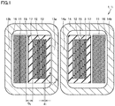
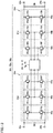
- Transformer 1 includes a first core 13, a first primary coil 11, a first secondary coil 12, and a first insulating member 15.
- transformer 1 may further include a second core 14 and may be a shell-type transformer.
- Transformer 1 may be a core-type transformer.
- First core 13 may include a first leg 13a and a second leg 13b opposed to first leg 13a.
- First core 13 may be a first ring core.
- First core 13 may be formed of a magnetic material having a low power loss, such as first amorphous magnetic material or first nanocrystalline magnetic material.
- the first nanocrystalline magnetic material may be, for example, an iron-based nanocrystalline magnetic material or a cobalt-based nanocrystalline magnetic material.
- the first amorphous magnetic material may be, for example, an iron-based amorphous magnetic material or a cobalt-based amorphous magnetic material. Even when the frequency of the power supplied to transformer 1 and the frequency of the power output from transformer 1 increase, the first amorphous magnetic material or the first nanocrystalline magnetic material included in first core 13 can reduce a power loss in first core 13.
- Second core 14 may include a third leg 14a facing first leg 13a and a fourth leg 14b opposed to third leg 14a.
- Second core 14 may be a second ring core.
- Second core 14 may be formed of a magnetic material having a low power loss, such as second amorphous magnetic material or second nanocrystalline magnetic material.
- the second nanocrystalline magnetic material may be, for example, an iron-based nanocrystalline magnetic material or a cobalt-based nanocrystalline magnetic material.
- the second amorphous magnetic material may be, for example, an iron-based amorphous magnetic material or a cobalt-based amorphous magnetic material.
- the second amorphous magnetic material or the second nanocrystalline magnetic material included in second core 14 can reduce a power loss in second core 14.
- the material for second core 14 may be identical to or different from the material for first core 13.
- First primary coil 11 includes a first conductor 16 wound around first core 13.
- First conductor 16 is wound around first leg 13a.
- First conductor 16 may be wound around second core 14.
- First conductor 16 may be wound around third leg 14a.
- First conductor 16 may be a conductive foil.
- the conductive foil refers to a conductor having a width larger than its thickness. In first conductor 16 formed of the conductive foil, a power loss in first primary coil 11 which results from the skin effect and the proximity effect in first primary coil 11, can be reduced.
- First secondary coil 12 includes a second conductor 17 wound around first core 13. Second conductor 17 is wound around first leg 13a. Second conductor 17 may be wound around second core 14. Second conductor 17 may be wound around third leg 14a. First secondary coil 12 may be disposed inside first primary coil 11. First secondary coil 12 may be disposed between first primary coil 11 and first leg 13a and between first primary coil 11 and third leg 14a. Second conductor 17 may be a first conductive foil. In second conductor 17 formed of the first conductive foil, a power loss in first secondary coil 12, which results from the skin effect and the proximity effect in first secondary coil 12, can be reduced.
- First secondary coil 12 is configured to be applied with a high voltage compared with first primary coil 11. A voltage of 25 kV or more may be applied to first secondary coil 12. Since a low voltage is applied to first primary coil 11 compared with first secondary coil 12, first primary coil 11 may not be covered with an insulating member. Since first primary coil 11 is not covered with an insulating member, first core 13 and second core 14 can be miniaturized.
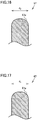
- second conductor 17 has the shape of a first polygon in a first cross-section of second conductor 17 perpendicular to the direction in which second conductor 17 extends.
- the polygon includes a polygon with a corner having a curvature.
- a first corner 17p of the first polygon has a first radius of curvature r 1 of 0.1 mm or more.
- First radius of curvature r 1 is equal to or less than a half of a first thickness d 1 of second conductor 17.
- Second conductor 17 with first corner 17p having first radius of curvature r 1 may be formed by processing second conductor 17 with a die.
- first insulating member 15 covers first secondary coil 12.
- First insulating member 15 may seal first secondary coil 12.
- First secondary coil 12 may be molded with first insulating member 15.
- First insulating member 15 may be formed of a resin material, such as epoxy resin or polyurethane resin.
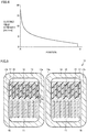
- FIG. 3 shows a distribution of an electric field strength in a region, which is indicated by line A-B in FIG. 1 , in transformer 1 of one example of Embodiment 1.
- a voltage of 25 kV is applied to first secondary coil 12
- first corner 17p has first radius of curvature r 1 of 0.1 mm
- first insulating member 15 is formed of the epoxy resin.
- the epoxy resin has a dielectric breakdown voltage of 15 kV/mm.
- a maximum value of the electric field strength around first secondary coil 12 is less than the electric field strength (15 kV/mm) that causes a dielectric breakdown in first insulating member 15.
- first corner 17p has first radius of curvature r 1 of 0.1 mm, an increase in the electric field strength in first insulating member 15, which results from the concentration of electric field at first corner 17p, can be restrained, which can prevent a dielectric breakdown of first insulating member 15.
- a minimum distance between first secondary coil 12 and first core 13 is 6 mm or more in the region in which the electric field strength between first secondary coil 12 and first core 13 becomes maximum.
- the region in which the electric field strength between first secondary coil 12 and first core 13 becomes maximum is the region indicated by line A-B in FIG. 1 .
- FIG. 4 shows a distribution of an electric field strength in a region indicated by line A-B in a transformer according to a comparative example.
- first corner 17p has an angle of 90°.
- the maximum value of the electric field strength around first secondary coil 12 is greater than an electric field strength (15 kV/mm) that causes a dielectric breakdown in first insulating member 15.
- first corner 17p since first corner 17p has an angle of 90°, a dielectric breakdown of first insulating member 15, which results from the concentration of electric field at first corner 17p, may occur.
- transformer 1 As described above, in transformer 1, the strength of an electric field applied to first insulating member 15 covering first secondary coil 12 can be reduced. A gap g 1 between adjacent portions of second conductor 17 can be reduced, leading to miniaturization of first secondary coil 12. Thus, first core 13 and second core 14 can be miniaturized, reducing a power loss in first core 13 and second core 14.
- Transformer 1 of the present Embodiment has improved power efficiency.
- the power efficiency herein refers to a ratio of the power output from a transformer to the power supplied to the transformer.
- first core 13 and second core 14 can be miniaturized.
- the material for first core 13 can be a magnetic material having a low power loss, such as first amorphous magnetic material or first nanocrystalline magnetic material.
- the material for second core 14 can be a magnetic material having a low power loss, such as second amorphous magnetic material or second nanocrystalline magnetic material.
- first primary coil 11 and first secondary coil 12 may be arranged in the direction in which first leg 13a and third leg 14a extend.
- Transformer 1a can have a relatively large gap G 1 between first primary coil 11 and first secondary coil 12 compared with transformer 1.
- Transformer 1a can have weak magnetic coupling between first primary coil 11 and first secondary coil 12 compared with transformer 1.
- Transformer 1a thus has a relatively high leakage inductance compared with transformer 1.
- Power converter 25 can be used in an offshore wind power generator or a DC power grid.
- Power converter 25 mainly includes a plurality of DC/DC converters 30.
- Power converter 25 may further include primary DC terminals 27a, 27b and secondary DC terminals 28a, 28b.
- DC/DC converters 30 each include primary terminals 31a, 31b, a DC/AC conversion circuit 33 connected to primary terminals 31a, 31b, transformer 1 (or transformer 1a), an AC/DC conversion circuit 34, and secondary terminals 32a, 32b connected to AC/DC conversion circuit 34.
- DC/DC converters 30 may each further include a first capacitor 38 connected in parallel with primary terminals 31a, 31b and a second capacitor 39 connected in parallel with secondary terminals 32a, 32b.
- DC/AC conversion circuit 33 is connected to first primary coil 11 and is a first single-phase bridge circuit.
- DC/AC conversion circuit 33 may be a first single-phase full-bridge circuit.
- DC/AC conversion circuit 33 may include a first switching circuit 45.
- First switching circuit 45 includes a plurality of first switching elements 41a, 41b, 41c, 41d and a plurality of first diodes 42a, 42b, 42c, 42d connected in anti-parallel with first switching elements 41a, 41b, 41c, 41d, respectively.
- First switching elements 41a, 41b, 41c, 41d may be transistors, such as insulated gate bipolar transistors (IGBTs).
- First switching circuit 45 includes two first legs 46a, 46b connected in parallel with each other.
- First leg 46a includes two first switching elements 41a, 41b connected in series with each other and two first diodes 42a, 42b connected in anti-parallel with two first switching elements 41a, 41b, respectively.
- First leg 46b includes two first switching elements 41c, 41d connected in series with each other and two first diodes 42c, 42d connected in anti-parallel with two first switching elements 41c, 41d, respectively.
- the opposite terminals (DC terminals) of each of two first legs 46a, 46b are connected to first capacitor 38.
- the midpoint (AC terminal) of each of two first legs 46a, 46b is connected to first primary coil 11 (first conductor 16) of transformer 1, 1a.
- the midpoint (AC terminal) of first leg 46a is located between first switching elements 41a, 41b.
- the midpoint (AC terminal) of first leg 46b is located between first switching elements 41c, 41d.
- AC/DC conversion circuit 34 is connected to first secondary coil 12 and is a second single-phase bridge circuit.
- AC/DC conversion circuit 34 may be a second single-phase full-bridge circuit.
- AC/DC conversion circuit 34 may include a second switching circuit 47.
- Second switching circuit 47 includes a plurality of second switching elements 43a, 43b, 43c, 43d and a plurality of second diodes 44a, 44b, 44c, 44d connected in anti-parallel with second switching elements 43a, 43b, 43c, 43d, respectively.
- Second switching elements 43a, 43b, 43c, 43d may be transistors, such as insulated gate bipolar transistors (IGBTs).
- Second switching circuit 47 includes two second legs 48a, 48b connected in parallel with each other.
- Second leg 48a includes two second switching elements 43a, 43b connected in series with each other and two second diodes 44a, 44b connected in anti-parallel with two second switching elements 43a, 43b, respectively.
- Second leg 48b includes two second switching elements 43c, 43d connected in series with each other and two second diodes 44c, 44d connected in anti-parallel with two second switching elements 43c, 43d, respectively.
- each of two second legs 48a, 48b are connected to second capacitor 39.
- the midpoint (AC terminal) of each of two second legs 48a, 48b is connected to a first secondary coil 12 (second conductor 17) of transformer 1, 1a.
- the midpoint (AC terminal) of second leg 48a is located between second switching elements 43a, 43b.
- the midpoint (AC terminal) of second leg 48b is located between second switching elements 43c, 43d.
- First switching elements 41a, 41b, 41c, 41d and second switching elements 43a, 43b, 43c, 43d may be configured to operate at frequencies of 100 Hz or more, may be configured to operate at frequencies of 200 Hz or more, or may be configured to operate at frequencies of 1 kHz or more.
- First switching elements 41a, 41b, 41c, 41d and second switching elements 43a, 43b, 43c, 43d may be configured to operate at frequencies of 2 kHz or less. Since first switching elements 41a, 41b, 41c, 41d and second switching elements 43a, 43b, 43c, 43d are configured to operate at high frequencies, each of DC/DC converters 30 can be miniaturized.
- first switching elements 41a, 41b, 41c, 41d and second switching elements 43a, 43b, 43c, 43d are operated at frequencies of, for example, 1 kHz or more
- first core 13 and second core 14 can be miniaturized.
- the material for first core 13a can be a magnetic material having a low power loss, such as first amorphous magnetic material or first nanocrystalline magnetic material.
- the material for second core 14A can be a magnetic material having a low power loss, such as second amorphous magnetic material or second nanocrystalline magnetic material.
- DC/DC converters 30 are connected to primary DC terminals 27a, 27b and secondary DC terminals 28a, 28b.
- Primary terminals 31a, 31b of DC/DC converters 30 are connected to primary DC terminals 27a, 27b.
- Primary terminals 31a, 31b of DC/DC converters 30 are connected in parallel with each other.
- Power converter 25 can thus handle high-current power.
- Secondary terminals 32a, 32b of DC/DC converters 30 are connected to secondary DC terminals 28a, 28b.
- Secondary terminals 32a, 32b of DC/DC converters 30 are connected in series with each other.
- power converter 25 can handle high-voltage power.
- Power converter 25 can convert low-voltage DC power of 1 kV to 3 kV into high-voltage DC power of 25 kV or more.
- transformer 1, 1a and power converter 25 of the present Embodiment will be described.
- Transformer 1, 1a of the present Embodiment includes first core 13, first primary coil 11, first secondary coil 12, and first insulating member 15.
- First primary coil 11 includes first conductor 16 wound around first core 13.
- First secondary coil 12 includes second conductor 17 wound around first core 13.
- First insulating member 15 covers first secondary coil 12.
- First secondary coil 12 is configured to be applied with a high voltage compared with first primary coil 11.
- Second conductor 17 has a shape of a first polygon in the first cross-section of second conductor 17 perpendicular to the direction in which second conductor 17 extends.
- First corner 17p of the first polygon has first radius of curvature r 1 of 0.1 mm or more.
- first corner 17p has first radius of curvature r 1 of 0.1 mm
- the dielectric breakdown of first insulating member 15 can be prevented.
- Transformer 1, 1a of the present Embodiment has improved dielectric breakdown voltage.
- First secondary coil 12 can be miniaturized.
- first core 13 can be miniaturized, reducing a power loss in first core 13.
- Transformer 1, 1a of the present Embodiment has improved power efficiency.
- second conductor 17 may be a first conductive foil. This can reduce a power loss in first secondary coil 12 which results from the skin effect and the proximity effect in first secondary coil 12. Transformer 1, 1a of the present Embodiment has improved power efficiency.
- first core 13 may be formed of the first amorphous magnetic material or the first nanocrystalline magnetic material.
- the power loss in first core 13 can be reduced even when the frequency of the power supplied to transformer 1, 1a and the frequency of the power output from transformer 1, 1a increase.
- Transformer 1, 1a of the present Embodiment has improved power efficiency.
- Transformer 1, 1a of the present Embodiment may further include second core 14.
- First core 13 may include first leg 13a and second leg 13b opposed to first leg 13a.
- Second core 14 may include third leg 14a facing first leg 13a and fourth leg 14b opposed to third leg 14a.
- First conductor 16 may be wound around first leg 13a and third leg 14a.
- Second conductor 17 may be wound around first leg 13a and third leg 14a.
- transformer 1, 1a of the present embodiment an increase in the electric field strength in first insulating member 15, which results from the concentration of electric field at first corner 17p, can be restrained. Thus, the dielectric breakdown of first insulating member 15 can be prevented.
- Transformer 1, 1a of the present Embodiment has improved dielectric breakdown voltage. Gap g 1 between adjacent portions of second conductor 17 can be reduced. Thus, first core 13 and second core 14 can be miniaturized, reducing a power loss in first core 13 and second core 14. Transformer 1, 1a of the present Embodiment has improved power efficiency.
- first secondary coil 12 may be disposed inside first primary coil 11.
- gap G 1 between first primary coil 11 and first secondary coil 12 can be reduced relatively.
- Magnetic coupling between first primary coil 11 and first secondary coil 12 can be increased.
- Transformer 1 having a relatively low leakage inductance can be provided.
- first primary coil 11 and first secondary coil 12 may be arranged in the direction in which first leg 13a and third leg 14a extend.
- gap G 1 between first primary coil 11 and first secondary coil 12 can be increased relatively.
- Magnetic coupling between first primary coil 11 and first secondary coil 12 can be weakened.
- Transformer 1a having a relatively high leakage inductance can be provided.
- second core 14 may be formed of the second amorphous magnetic material or the second nanocrystalline magnetic material.
- the power loss in second core 14 can be reduced even when the frequency of the power supplied to transformer 1, 1a and the frequency of the power output from transformer 1, 1a increase.
- Transformer 1, 1a of the present Embodiment has improved power efficiency.
- Power converter 25 of the present Embodiment includes DC/DC converters 30.
- DC/DC converters 30 each include primary terminals 31a, 31b, DC/AC conversion circuit 33 connected to primary terminals 31a, 31b, AC/DC conversion circuit 34, and secondary terminals 32a, 32b connected to AC/DC conversion circuit 34.
- DC/AC conversion circuit 33 is connected to first primary coil 11 and is a first single-phase bridge circuit.
- AC/DC conversion circuit 34 is connected to first secondary coil 12 and is a second single-phase bridge circuit.
- Primary terminals 31a, 31b of DC/DC converters 30 are connected in parallel with each other.
- Secondary terminals 32a, 32b of DC/DC converters 30 are connected in series with each other.
- Power converter 25 of the present Embodiment has improved dielectric breakdown voltage and improved power efficiency.
- transformer 1b according to Embodiment 2 will be described with reference to FIGS. 8 and 9 .
- transformer 1b of the present Embodiment includes components similar to the components of transformer 1 of Embodiment 1, it differs from that of Embodiment 1 mainly in the following respects.
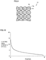
- second conductor 18 is a first litz wire formed of a plurality of twisted first conductive strands 19.
- First conductive strands 19 each have the shape of a circle having a first radius R 1 of 0.1 mm or more in the first cross-section of second conductor 18.
- the circle shapes include not only the shape of a circle but also the shape of an oval in which a ratio of its major axis to its minor axis is 1.0 or more and 1.5 or less, and first radius R 1 of 0.1 mm or more refers to a minor axis of 0.1 mm or more.
- second conductor 18 has a first corner 18p having first radius of curvature r 1 defined by first radius R 1 of first conductive strand 19.
- FIG. 10 shows a distribution of an electric field strength of the region indicated by line A-B in FIG. 8 in transformer 1b of one example of Embodiment 2.
- a maximum value of the electric field strength around first secondary coil 12 is less than the electric field strength (15 kV/mm) that causes a dielectric breakdown in first insulating member 15.
- first conductive strands 19 each have the shape of a circle having first radius R 1 of 0.1 mm or more, an increase in the electric field strength in first insulating member 15, which results from the concentration of electric field at first corner 18p, can be restrained, thus preventing a dielectric breakdown of first insulating member 15. Further, it is not necessary to process second conductor 18 in the present embodiment, unlike in Embodiment 1.
- Transformer 1b of the present Embodiment can thus be manufactured at low cost compared with transformer 1 of Embodiment 1.
- first primary coil 11 and first secondary coil 12 may be arranged in the direction in which first leg 13a and third leg 14a extend.
- gap G 1 between first primary coil 11 and first secondary coil 12 can be relatively large compared with transformer 1b.
- magnetic coupling between first primary coil 11 and first secondary coil 12 can be weak compared with transformer 1b.
- transformer 1c has a relatively high leakage inductance compared with transformer 1b.
- a power converter 25b according to Embodiment 2 will be described with reference to FIGS. 6 and 7 .
- power converter 25b of the present Embodiment includes components similar to the components of power converter 25 of Embodiment 1, it differs from that of Embodiment 1 in that transformer 1, 1a of Embodiment 1 is replaced by transformer 1b, 1c of the present embodiment.
- Transformer 1b, 1c and power converter 25b of the present Embodiment achieve the following effects similar to the components of transformer 1, 1a and power converter 25 of Embodiment 1.
- second conductor 18 is a first litz wire formed of twisted first conductive strands 19.
- First conductive strands 19 each have the shape of a circle having first radius R 1 of 0.1 mm or more in the first cross-section of second conductor 18.
- a power converter 25d according to Embodiment 3 will be described with reference to FIGS. 12 to 14 .
- power converter 25d of the present Embodiment includes components similar to the components of power converter 25 of Embodiment 1, it differs from that of Embodiment 1 mainly in the following respects.
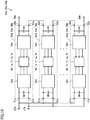
- Power converter 25d of the present Embodiment includes a plurality of DC/DC converters 30d. As shown in FIGS. 12 and 13 , DC/DC converters 30d each include primary terminals 31a, 31b, a DC/AC conversion circuit 33d connected to primary terminals 31a, 31b, a transformation unit 40, an AC/DC conversion circuit 34d, and secondary terminals 32a, 32b connected to AC/DC conversion circuit 34d.
- transformation unit 40 includes any three of transformers 1, 1a, 1b, 1c of Embodiment 1 and Embodiment 2.
- DC/AC conversion circuits 33d are connected to first primary coils 11 of transformation units 40 (three transformers 1, 1a, 1b, 1c). Specifically, first terminals of first primary coils 11 of three transformers 1, 1a, 1b, 1c are connected to DC/AC conversion circuits 33d. Second terminals of first primary coils 11 of three transformers 1, 1a, 1b, 1c are connected to each other.
- DC/AC conversion circuit 33d is a first three-phase bridge circuit.
- DC/AC conversion circuit 33d may be a first three-phase full-bridge circuit.
- DC/AC conversion circuit 33d may include a first switching circuit 45d.
- first switching circuit 45d includes a plurality of first switching elements 41a, 41b, 41c, 41d, 41e, 41f and a plurality of first diodes 42a, 42b, 42c, 42d, 42e, 42f connected in anti-parallel with first switching elements 41a, 41b, 41c, 41d, 41e, 41f, respectively.
- First switching elements 41a, 41b, 41c, 41d, 41e, 41f may be transistors, such as insulated gate bipolar transistors (IGBTs).
- First switching circuit 45d includes three first legs 46a, 46b, 46c connected in parallel with each other.
- First leg 46a includes two first switching elements 41a, 41b connected in series with each other and two first diodes 42a, 42b connected in anti-parallel with two first switching elements 41a, 41b, respectively.
- First leg 46b includes two first switching elements 41c, 41d connected in series with each other and two first diodes 42c, 42d connected in anti-parallel with two first switching elements 41c, 41d, respectively.
- First leg 46c includes two first switching elements 41e, 41f connected in series with each other and two first diodes 42e, 42f connected in anti-parallel with two first switching elements 41e, 41f, respectively.
- the opposite terminals (DC terminals) of each of three first legs 46a, 46b, 46c are connected to first capacitor 38.
- the midpoint (AC terminal) of each of three first legs 46a, 46b, 46c is connected to a corresponding one of three first primary coils 11 (first conductors 16) of three transformers 1, 1a, 1b, 1c.
- the midpoint (AC terminal) of first leg 46a is located between two first switching elements 41a, 41b.
- the midpoint (AC terminal) of first leg 46b is located between two first switching elements 41c, 41d.
- the midpoint (AC terminal) of first leg 46c is located between two first switching elements 41e, 41f.
- AC/DC conversion circuits 34d are connected to first secondary coils 12 of transformation units 40 (three transformers 1, 1a, 1b, 1c). Specifically, first terminals of first secondary coils 12 of three transformers 1, 1a, 1b, 1c are connected to AC/DC conversion circuit 34d. Second terminals of first secondary coils 12 of three transformers 1, 1a, 1b, 1c are connected to each other.
- AC/DC conversion circuit 34d is a second three-phase bridge circuit.
- AC/DC conversion circuit 34d may be a second three-phase full-bridge circuit.
- AC/DC conversion circuit 34d may include second switching circuit 47d.
- second switching circuit 47d includes a plurality of second switching elements 43a, 43b, 43c, 43d, 43e, 43f and a plurality of second diodes 44a, 44b, 44c, 44d, 44e, 44f connected in anti-parallel with second switching elements 43a, 43b, 43c, 43d, 43e, 43f, respectively.
- Second switching elements 43a, 43b, 43c, 43d, 43e, 43f may be transistors, such as insulated gate bipolar transistors (IGBTs).
- Second switching circuit 47d includes three second legs 48a, 48b, 48c connected in parallel with each other.
- Second leg 48a includes two second switching elements 43a, 43b connected in series with each other and two second diodes 44a, 44b connected in anti-parallel with two second switching elements 43a, 43b, respectively.
- Second leg 48b includes two second switching elements 43c, 43d connected in series with each other and two second diodes 44c, 44d connected in anti-parallel with two second switching elements 43c, 43d, respectively.
- Second leg 48c includes two second switching elements 43e, 43f connected in series with each other and two second diodes 44e, 44f connected in anti-parallel with two second switching elements 43e, 43f, respectively.
- each of three second legs 48a, 48b, 48c are connected to second capacitor 39.
- Each of the midpoints (AC terminals) of three second legs 48a, 48b, 48c is connected to a corresponding one of three first secondary coils 12 (second conductors 17) of three transformers 1, 1a, 1b, 1c.
- the midpoint (AC terminal) of second leg 48a is located between two second switching elements 43a, 43b.
- the midpoint (AC terminal) of second leg 48b is located between two second switching elements 43c, 43d.
- the midpoint (AC terminal) of second leg 48c is located between two second switching elements 43e, 43f.
- First switching elements 41a, 41b, 41c, 41d, 41e, 41f and second switching elements 43a, 43b, 43c, 43d, 43e, 43f may be configured to operate at frequencies of 100 Hz or more, may be configured to operate at frequencies of 200 Hz or more, or may be configured to operate at frequencies of 1 kHz or more.
- First switching elements 41a, 41b, 41c, 41d, 41e, 41f and second switching elements 43a, 43b, 43c, 43d, 43e, 43f may be configured to operate at frequencies of 2 kHz of less.
- first switching elements 41a, 41b, 41c, 41d, 41e, 41f and second switching elements 43a, 43b, 43c, 43d, 43e, 43f are configured to operate at high frequencies, each of DC/DC converters 30d can be miniaturized.
- first switching elements 41a, 41b, 41c, 41d, 41e, 41f and second switching elements 43a, 43b, 43c, 43d, 43e, 43f are operated at, for example, frequencies of 1 kHz or more
- first core 13 and second core 14 can be miniaturized.
- the material for first core 13 can be a magnetic material having a low power loss, such as first amorphous magnetic material or first nanocrystalline magnetic material.
- the material for second core 14 can be a magnetic material having a low power loss, such as second amorphous magnetic material or second nanocrystalline magnetic material.
- DC/DC converters 30d are connected to primary DC terminals 27a, 27b and secondary DC terminals 28a, 28b.
- Primary terminals 31a, 31b of DC/DC converters 30d are connected to primary DC terminals 27a, 27b.
- Primary terminals 31a, 31b of DC/DC converters 30d are connected in parallel with each other.
- power converter 25d can handle high-current power.
- Secondary terminals 32a, 32b of DC/DC converters 30d are connected to secondary DC terminals 28a, 28b.
- Secondary terminals 32a, 32b of DC/DC converters 30d are connected in series with each other.
- power converter 25d can handle high-voltage power.
- Power converter 25d can convert low-voltage DC power of 1 kV to 3 kV into high-voltage DC power of 25 kV or more.
- Power converter 25d of the present Embodiment achieves the following effects in addition to the effects of power converter 25 of Embodiment 1.
- Power converter 25d of the present Embodiment includes DC/DC converters 30d.
- DC/DC converters 30d each include primary terminals 31a, 31b, DC/AC conversion circuit 33d connected to primary terminals 31a, 31b, transformation unit 40, AC/DC conversion circuit 34d, and secondary terminals 32a, 32b connected to AC/DC conversion circuit 34d.
- Transformation unit 40 includes any three of transformers 1, 1a, 1b, 1c of Embodiment 1 and Embodiment 2.
- Each of DC/AC conversion circuits 33d is connected to a corresponding one of first primary coils 11 of three transformers 1, 1a, 1b, 1c and is a first three-phase bridge circuit.
- Each of AC/DC conversion circuits 34d is connected to a corresponding one of first secondary coils 12 of three transformers 1, 1a, 1b, 1c and is a second three-phase bridge circuit.
- Primary terminals 31a, 31b of DC/DC converters 30d are connected in parallel with each other.
- Secondary terminals 32a, 32b of DC/DC converters 30d are connected in series with each other.
- Power converter 25d of the present Embodiment has improved dielectric breakdown voltage and improved power efficiency.
- power converter 25d of the present Embodiment is a three-phase power converter, a current flowing through transformer 1, 1a, 1b, 1c can be reduced.
- the power loss in first switching elements 41a, 41b, 41c, 41d, 41e, 41f and second switching elements 43a, 43b, 43c, 43d, 43e, 43f and the power loss in first primary coil 11 and first secondary coil 12 can be reduced.
- first core 13 and second core 14 can be miniaturized.
- the material for first core 13 can be a magnetic material having a low power loss, such as first amorphous magnetic material or first nanocrystalline magnetic material.
- the material for second core 14 can be a magnetic material having a low power loss, such as second amorphous magnetic material or second nanocrystalline magnetic material.
- Power converter 25d of the present Embodiment has improved power efficiency.
- Transformer 1e of the present Embodiment includes components similar to the components of transformer 1 of Embodiment 1, it differs from that of Embodiment 1 mainly in the following respects.
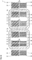
- Transformer 1e of the present Embodiment further includes a second primary coil 51, a second secondary coil 52, a second insulating member 55, a third primary coil 61, a third secondary coil 62, and a third insulating member 65.
- Second primary coil 51 includes a third conductor 56 wound around first core 13.
- Third conductor 56 is wound around second leg 13b.
- Third conductor 56 may be a conductive foil.
- a power loss in second primary coil 51 which results from the skin effect and the proximity effect in second primary coil 51, can be reduced.
- Second secondary coil 52 includes a fourth conductor 57 wound around first core 13. Fourth conductor 57 is wound around second leg 13b. Second secondary coil 52 may be disposed inside second primary coil 51. Second secondary coil 52 may be disposed between second primary coil 51 and second leg 13b. Fourth conductor 57 may be a second conductive foil. In fourth conductor 57 formed of the second conductive foil, a power loss in second secondary coil 52, which results from the skin effect and the proximity effect in second secondary coil 52, can be reduced.
- Second secondary coil 52 is configured to be applied with a high voltage compared with second primary coil 51.
- a voltage of 25 kV or more may be applied to second secondary coil 52. Since a low voltage is applied to second primary coil 51 compared with second secondary coil 52, second primary coil 51 may not be covered with an insulating member. Since second primary coil 51 is not covered with the insulating member, first core 13 can be miniaturized.
- fourth conductor 57 has the shape of a second polygon in a second cross-section of fourth conductor 57 perpendicular to the direction in which fourth conductor 57 extends.
- a second corner 57p of the second polygon has a second radius of curvature r 2 of 0.1 mm or more. This can restrain an increase in the electric field strength, which results from the concentration of electric field at second corner 57p, thus preventing a dielectric breakdown of second insulating member 55.
- Second radius of curvature r 2 is equal to or less than a half of a thickness d 2 of fourth conductor 57.
- Fourth conductor 57 with second corner 57p having second radius of curvature r 2 may be formed by processing fourth conductor 57 with a die.
- Second radius of curvature r 2 may be equal to first radius of curvature r 1 , may be greater than first radius of curvature r 1 , or may be smaller than first radius of curvature r 1 .
- Second insulating member 55 covers second secondary coil 52. Second insulating member 55 may seal second secondary coil 52. Second secondary coil 52 may be molded with second insulating member 55. Second insulating member 55 may be formed of a resin material, such as epoxy resin or polyurethane resin.
- Third primary coil 61 includes a fifth conductor 66 wound around second core 14. Fifth conductor 66 is wound around fourth leg 14b. Fifth conductor 66 may be a conductive foil. In fifth conductor 66 formed of the conductive foil, a power loss in third primary coil 61, which results from the skin effect and the proximity effect in third primary coil 61, can be reduced.
- Third secondary coil 62 includes a sixth conductor 67 wound around second core 14. Sixth conductor 67 is wound around fourth leg 14b. Third secondary coil 62 may be disposed inside third primary coil 61. Third secondary coil 62 may be disposed between third primary coil 61 and fourth leg 14b. Sixth conductor 67 may be a third conductive foil. In sixth conductor 67 formed of the third conductive foil, a power loss in third secondary coil 62, which results from the skin effect and the proximity effect in third secondary coil 62, can be reduced.
- Third secondary coil 62 is configured to be applied with a high voltage compared with third primary coil 61.
- a voltage of 25 kV or more may be applied to third secondary coil 62. Since a low voltage is applied to third primary coil 61 compared with third secondary coil 62, third primary coil 61 may not be covered with the insulating member. Since third primary coil 61 is not covered with the insulating member, second core 14 can be miniaturized.
- sixth conductor 67 has the shape of a third polygon in a third cross-section of sixth conductor 67 perpendicular to the direction in which sixth conductor 67 extends.
- a third corner 67p of the third polygon has a third radius of curvature r 3 of 0.1 mm or more.
- Third radius of curvature r 3 is equal to or less than a half of a thickness d 3 of sixth conductor 67.
- Sixth conductor 67 with third corner 67p having third radius of curvature r 3 may be formed by processing sixth conductor 67 with a die.
- Third radius of curvature r 3 may be equal to first radius of curvature r 1 , may be greater than first radius of curvature r 1 , or may be smaller than first radius of curvature r 1 .
- Third radius of curvature r 3 may be equal to second radius of curvature r 2 , may be greater than second radius of curvature r 2 , or may be smaller than second radius of curvature r 2 .
- Third insulating member 65 covers third secondary coil 62. Third insulating member 65 may seal third secondary coil 62. Third secondary coil 62 may be molded with third insulating member 65. Third insulating member 65 may be formed of a resin material, such as epoxy resin or polyurethane resin.
- transformer 1e the strength of an electric field applied to second insulating member 55 covering second secondary coil 52 can be reduced. A gap g 2 between adjacent portions of fourth conductor 57 can be reduced, leading to miniaturization of second secondary coil 52.
- first core 13 can be miniaturized, reducing a power loss in first core 13.
- Transformer 1e has improved power efficiency. It is generally difficult to increase the size of a core formed of an amorphous magnetic material or a nanocrystalline magnetic material. Since first core 13 can be miniaturized in transformer 1e, the material for first core 13 can be a magnetic material having a low power loss, such as first amorphous magnetic material or first nanocrystalline magnetic material.
- transformer 1e the strength of an electric field applied to third insulating member 65 covering third secondary coil 62 can be reduced. A gap g 3 between adjacent portions of sixth conductor 67 can be reduced, leading to miniaturization of third secondary coil 62.
- second core 14 can be miniaturized, reducing a power loss in second core 14.
- Transformer 1e has improved power efficiency. It is generally difficult to increase the size of a core formed of an amorphous magnetic material or a nanocrystalline magnetic material. Since second core 14 can be miniaturized in transformer 1e, the material for second core 14 can be a magnetic material having a low power loss, such as second amorphous magnetic material or second nanocrystalline magnetic material.
- second primary coil 51 and second secondary coil 52 may be arranged in the direction in which second leg 13b extends.
- Third primary coil 61 and third secondary coil 62 may be arranged in the direction in which fourth leg 14b extends.
- a gap G 2 between second primary coil 51 and second secondary coil 52 can be relatively large compared with transformer 1e.
- a gap G 3 between third primary coil 61 and third secondary coil 62 can be relatively large compared with transformer 1e.
- magnetic coupling between second primary coil 51 and second secondary coil 52 can be weak compared with transformer 1e.
- magnetic coupling between third primary coil 61 and third secondary coil 62 can be weak compared with transformer 1e.
- Transformer 1f has a relatively high leakage inductance compared with transformer 1e.
- a power converter 25e according to Embodiment 4 will be described with reference to FIGS. 12 , 13 , and 19 .
- power converter 25e of the present Embodiment includes components similar to the components of power converter 25d of Embodiment 3, it differs from that of Embodiment 3 mainly in that in power converter 25e of the present embodiment, transformation unit 40 of Embodiment 3 is replaced by transformer 1e or transformer 1f of the present embodiment.
- Power converter 25e of the present Embodiment includes a plurality of DC/DC converters 30e.
- DC/DC converter 30e of the present Embodiment includes components similar to the components of DC/DC converter 30d of Embodiment 3, it differs from that of Embodiment 3 mainly in that transformation unit 40 of Embodiment 3 is replaced by transformer 1e or transformer 1f of the present embodiment.
- DC/DC converters 30e each include primary terminals 31a, 31b, DC/AC conversion circuit 33d connected to primary terminals 31a, 31b, transformer 1e, 1f, AC/DC conversion circuit 34d, and secondary terminals 32a, 32b connected to AC/DC conversion circuit 34d.
- DC/AC conversion circuit 33d is connected to first primary coil 11, second primary coil 51, and third primary coil 61 and is a first three-phase bridge circuit.
- DC/AC conversion circuit 33d may be a first three-phase full-bridge circuit.
- AC/DC conversion circuit 34d is connected to first secondary coil 12, second secondary coil 52, and third secondary coil 62 and is a second three-phase bridge circuit.
- AC/DC conversion circuit 34d may be a second three-phase full-bridge circuit.
- Power converter 25e can handle high-current power. Secondary terminals 32a, 32b of DC/DC converters 30e are connected in series with each other. Thus, power converter 25e can handle high-voltage power. Power converter 25e can convert low-voltage DC power of 1 kV to 3 kV into high-voltage DC power of 25 kV or more.
- Transformer 1e, 1f and power converter 25e of the present Embodiment achieve the following effects in addition to the effects of transformer 1d and power converter 25d of Embodiment 3.
- Transformer 1e, 1f of the present Embodiment further includes second primary coil 51, second secondary coil 52, second insulating member 55, third primary coil 61, third secondary coil 62, and third insulating member 65.
- Second primary coil 51 includes third conductor 56 wound around second leg 13b.
- Second secondary coil 52 includes fourth conductor 57 wound around second leg 13b.
- Second insulating member 55 covers second secondary coil 52.
- Third primary coil 61 includes fifth conductor 66 wound around fourth leg 14b.
- Third secondary coil 62 includes sixth conductor 67 wound around fourth leg 14b.
- Third insulating member 65 covers third secondary coil 62.
- Second secondary coil 52 is configured to be applied with a high voltage compared with second primary coil 51.
- Third secondary coil 62 is configured to be applied with a high voltage compared with third primary coil 61.
- Fourth conductor 57 has the shape of the second polygon in the second cross-section of fourth conductor 57 perpendicular to the direction in which fourth conductor 57 extends.
- Second corner 57p of the second polygon has second radius of curvature r 2 of 0.1 mm or more.
- Sixth conductor 67 has the shape of the third polygon in the third cross-section of sixth conductor 67 perpendicular to the direction in which sixth conductor 67 extends.
- Third corner 67p of the third polygon has third radius of curvature r 3 of 0.1 mm or more.
- transformer 1e, 1f of the present Embodiment has improved dielectric breakdown voltage.
- Gap g 2 between adjacent portions of fourth conductors 57 and gap g 3 between adjacent portions of sixth conductors 67 can be reduced, leading to miniaturization of second secondary coil 52 and third secondary coil 62.
- first core 13 and second core 14 can be miniaturized, reducing a power loss in first core 13 and second core 14.
- Transformer 1e, 1f of the present Embodiment has improved power efficiency.
- first primary coil 11, first secondary coil 12, second primary coil 51, second secondary coil 52, third primary coil 61, and third secondary coil 62 can be disposed compactly in first core 13 and second core 14. According to transformer 1e, 1f of the present embodiment, a compact three-phase transformer can be obtained.
- fourth conductor 57 may be the second conductive foil
- sixth conductor 67 may be the third conductive foil.
- second secondary coil 52 may be disposed inside second primary coil 51.
- Third secondary coil 62 may be disposed inside third primary coil 61. Gap G 2 between second primary coil 51 and second secondary coil 52 can thus be reduced relatively. Magnetic coupling between second primary coil 51 and second secondary coil 52 can be increased. Gap G 3 between third primary coil 61 and third secondary coil 62 can be reduced relatively. Magnetic coupling between third primary coil 61 and third secondary coil 62 can be increased.
- Transformer 1e having a relatively low leakage inductance can be provided.
- second primary coil 51 and second secondary coil 52 may be arranged in the direction in which second leg 13b extends.
- Third primary coil 61 and third secondary coil 62 may be arranged in the direction in which fourth leg 14b extends.
- gap G 2 between second primary coil 51 and second secondary coil 52 can be increased relatively.
- Magnetic coupling between second primary coil 51 and second secondary coil 52 can be weakened.
- Gap G 3 between third primary coil 61 and third secondary coil 62 can be increased relatively.
- Magnetic coupling between third primary coil 61 and third secondary coil 62 can be weakened.
- Transformer 1f having a relatively high leakage inductance can be provided.
- Power converter 25e of the present Embodiment includes DC/DC converters 30e.
- DC/DC converters 30e can each include primary terminals 31a, 31b, DC/AC conversion circuit 33d connected to primary terminals 31a, 31b, transformer 1e, 1f, AC/DC conversion circuit 34d, and secondary terminals 32a, 32b connected to AC/DC conversion circuit 34d.
- DC/AC conversion circuit 33d is connected to first primary coil 11, second primary coil 51, and third primary coil 61 and is a first three-phase bridge circuit.
- AC/DC conversion circuit 34d is connected to first secondary coil 12, second secondary coil 52, and third secondary coil 62 and is a second three-phase bridge circuit.
- Primary terminals 31a, 31b of DC/DC converters 30e are connected in parallel with each other.
- Secondary terminals 32a, 32b of DC/DC converters 30e are connected in series with each other.
- Power converter 25e of the present Embodiment has improved dielectric breakdown voltage and improved power efficiency.
- transformer 1g according to Embodiment 5 will be described with reference to FIGS. 20 to 22 .
- transformer 1g of the present Embodiment includes components similar to the components of transformer 1e of Embodiment 4, it differs from that of Embodiment 4 mainly in the following respects.
- a fourth conductor 58 is a second litz wire formed of a plurality of twisted second conductive strands 59.
- Second conductive strands 59 each have the shape of a circle having a second radius R 2 of 0.1 mm or more in the second cross-section.
- fourth conductor 58 has a second corner 58p having second radius of curvature r 2 which is defined by second radius R 2 of second conductive strand 59.
- Second radius R 2 may be equal to first radius R 1 , may be greater than first radius R 1 , or may be smaller than first radius R 1 .
- a sixth conductor 68 is a third litz wire formed of a plurality of twisted third conductive strands 69.
- Third conductive strands 69 each have the shape of a circle having a third radius R 3 of 0.1 mm or more in the third cross-section.
- sixth conductor 68 has a third corner 68p having third radius of curvature r 3 which is defined by third radius R 3 of third conductive strand 69.
- Third radius R 3 may be equal to first radius R 1 , may be greater than first radius R 1 , or may be smaller than first radius R 1 . Third radius R 3 may be equal to second radius R 2 , may be greater than second radius R 2 , or may be smaller than second R 2 .
- Transformer 1g of the present Embodiment can thus be manufactured at low cost compared with transformer 1e of Embodiment 4.
- second primary coil 51 and second secondary coil 52 may be arranged in the direction in which second leg 13b extends.
- gap G 2 between second primary coil 51 and second secondary coil 52 can be relatively large compared with transformer 1g.
- magnetic coupling between second primary coil 51 and second secondary coil 52 can be weak compared with transformer 1g.
- third primary coil 61 and third secondary coil 62 may be arranged in the direction in which fourth leg 14b extends.
- gap G 3 between third primary coil 61 and third secondary coil 62 can be relatively large compared with transformer 1g.
- magnetic coupling between third primary coil 61 and third secondary coil 62 can be weak compared with transformer 1g.
- Transformer 1h thus has a relatively high leakage inductance compared with transformer 1g.
- a power converter 25g according to Embodiment 5 will be described with reference to FIGS. 12 , 13 , and 19 .
- power converter 25g of the present Embodiment includes components similar to the components of power converter 25e of Embodiment 4, it differs from that of Embodiment 4 in that transformer 1e, 1f of Embodiment 4 is replaced by transformer 1g or transformer 1h of the present embodiment.
- power converter 25g of the present Embodiment includes a plurality of DC/DC converters 30g.
- DC/DC converter 30g includes components similar to the components of DC/DC converters 30e of Embodiment 4, it differs from that of Embodiment 4 mainly in that transformer 1e, 1f of Embodiment 4 is replaced by transformer 1g or transformer 1h of the present embodiment.
- Transformer 1g, 1h and power converter 25g of the present Embodiment achieve the following effects similar to the components of transformer 1e and power converter 25e of Embodiment 4.
- fourth conductor 58 may be a second litz wire formed of a plurality of twisted second conductive strands 59.
- Sixth conductor 68 may be a third litz wire formed of a plurality of twisted third conductive strands 69.
- Second conductive strands 59 may each have the shape of a circle having second radius R 2 of 0.1 mm or more in the second cross-section of fourth conductor 58.
- Third conductive strands 69 may each have the shape of a circle having third radius R 3 of 0.1 mm or more in the third cross-section of sixth conductor 68.
- Transformer 1g, 1h and power converter 25g of the present Embodiment have improved dielectric breakdown voltage and improved power efficiency.
- transformer 1i according to Embodiment 6 will be described with reference to FIGS. 1 and 2 .
- transformer 1i of the present Embodiment includes components similar to the components of transformer 1 of Embodiment 1, it differs from that of Embodiment 1 mainly in the following respects.
- a first inductance of first primary coil 11 is equal to a second inductance of first secondary coil 12.
- the first inductance of first primary coil 11 is measured by opening all the coils (including first secondary coil 12) except for first primary coil 11 and directly connecting a measuring instrument, such as an LCR meter, to the opposite ends (see the white circles of first primary coil 11 in FIG. 7 ) of first primary coil 11.
- the second inductance of first secondary coil 12 is measured by opening all the coils (including first primary coil 11) except for first secondary coil 12 and directly connecting a measuring instrument, such as an LCR meter, to the opposite ends (see the white circles of first secondary coil 12 in FIG. 7 ) of first secondary coil 12.
- the inductance of a coil depends on the length of the coil, the shape of the coil, the distance between a core and the coil, and the like.
- the inductance of the coil decreases as the length of the coil along the core decreases.
- the inductance of the coil decreases as the distance between the coil and the core increases.
- the length of first primary coil 11 along first leg 13a of first core 13 and third leg 14a of second core 14 is larger than the length of first secondary coil 12 along first leg 13a and third leg 14a.
- the distance between first leg 13a, third leg 14a and first primary coil 11 is larger than the distance between first leg 13a, third leg 14a and first secondary coil 12.
- the first inductance of first primary coil 11 can be made equal to the second inductance of first secondary coil 12.
- first primary coil 11 when a voltage is applied to between primary terminals 31a, 31b, the voltage is applied to first primary coil 11 via DC/AC conversion circuit 33.
- First primary coil 11 applied with the voltage excites a magnetic flux in first leg 13a of first core 13 and third leg 14a of second core 14. This magnetic flux causes an induced voltage in first secondary coil 12. Since the first inductance of first primary coil 11 is equal to the second inductance of first secondary coil 12, the same magnetic flux as that of first primary coil 11 is excited also in first secondary coil 12, causing the induced voltage to be equal to the voltage applied to first secondary coil 12 by second switching circuit 47. This prevents a flow of reactive current through second switching circuit 47, thus preventing a power loss in second switching elements 43a, 43b, 43c, 43d.
- first secondary coil 12 when a voltage is applied to between secondary terminals 32a, 32b, the voltage is applied to first secondary coil 12 via AC/DC conversion circuit 34.
- First secondary coil 12 applied with the voltage excites a magnetic flux in first leg 13a of first core 13 and third leg 14a of second core 14.
- This magnetic flux causes an induced voltage in first primary coil 11. Since the first inductance of first primary coil 11 is equal to the second inductance of first secondary coil 12, the same magnetic flux as that of first secondary coil 12 is excited also in first primary coil 11, causing the induced voltage to be equal to the voltage applied to first primary coil 11 by first switching circuit 45. This prevents a flow of reactive current through first switching circuit 45, thus preventing a power loss in first switching elements 41a, 41b, 41c, 41d.
- Transformer 1i of the present Embodiment achieves the effect of having improved power efficiency in addition to the effects of transformer 1 of Embodiment 1.
- the first inductance of first primary coil 11 is made equal to the second inductance of first secondary coil 12 in transformer 1 of Embodiment 1 in the present embodiment
- the first inductance of first primary coil 11 may be equal to the second inductance of first secondary coil 12 also in Embodiment 2 to Embodiment 5 and the modifications of Embodiment 1 to Embodiment 5.
- the inductance of second primary coil 51 and the inductance of second secondary coil 52 may be equal to each other, and the inductance of third primary coil 61 and the inductance of third secondary coil 62 may be equal to each other.
- Embodiments 1 to 6 and the modifications thereof disclosed herein are illustrative and non-restrictive in every respect. At least two of Embodiments 1 to 6 and the modifications thereof disclosed herein may be combined within a range free of inconsistency or contradiction.
- the scope of the present invention is defined by the terms of the claims, rather than the description of the embodiments above, and is intended to include any modifications within the scope and meaning equivalent to the terms of the claims.
Landscapes
- Engineering & Computer Science (AREA)
- Power Engineering (AREA)
- Dc-Dc Converters (AREA)
- Coils Of Transformers For General Uses (AREA)
Abstract
Description
- The present invention relates to a transformer and a power converter.
- US Patent
US 5 027 264 A (PTL 1) discloses a DC/DC transformer including a transformer. - PTL 1: US Patent
US 5 027 264 A - An object of the present invention is to provide a transformer and a power converter that have improved dielectric breakdown voltage and improved power efficiency.
- A transformer according to the present invention includes a first core, a first primary coil, a first secondary coil, and a first insulating member. The first primary coil includes a first conductor wound around the first core. The first secondary coil includes a second conductor wound around the first core. The first insulating member covers the first secondary coil. The first secondary coil is applied with a high voltage compared with the first primary coil. The second conductor has a shape of a first polygon in a first cross-section of the second conductor perpendicular to a direction in which the second conductor extends. A first corner of the first polygon has a first radius of curvature of 0.1 mm or more.
- A power converter of the present invention includes the transformer.
- Since the first corner has the first radius of curvature of 0.1 mm, an increase in electric field strength, which results from the concentration of electric field at the first corner, can be restrained. Consequently, a dielectric breakdown of the first insulating member, which results from the concentration of electric field at the first corner, can be restrained. Also, the first secondary primary coil can be miniaturized, leading to miniaturization of the first core. The transformer of the present invention and the power converter of the present invention have improved dielectric breakdown voltage and improved power efficiency.
-
- FIG. 1
- is a schematic sectional view of a transformer according to each of
Embodiment 1 and Embodiment 6. - FIG. 2
- is a partially enlarged schematic sectional view of a region II, shown in
FIG. 1 , of the transformer according to each ofEmbodiment 1 and Embodiment 6. - FIG. 3
- shows a distribution of an electric field strength in A-B, shown in
FIG. 1 , of a transformer of an example ofEmbodiment 1. - FIG. 4
- shows a distribution of an electric field strength in A-B of a transformer according to a comparative example.
- FIG. 5
- is a schematic sectional view of a transformer according to a modification of
Embodiment 1. - FIG. 6
- is a circuit diagram of a power converter according to each of
Embodiment 1 and Embodiment 2. - FIG. 7
- is a partially enlarged circuit diagram of the power converter according to each of
Embodiment 1 and Embodiment 2. - FIG. 8
- is a schematic sectional view of a transformer according to Embodiment 2.
- FIG. 9
- is a partially enlarged schematic sectional view of a region IX, shown in
FIG. 8 , of the transformer according to Embodiment 2. - FIG.
- 10 shows a distribution of an electric field strength in A-B, shown in
FIG. 8 , of a transformer of an example of Embodiment 2. - FIG. 11
- is a schematic sectional view of a transformer according to a modification of Embodiment 2.
- FIG. 12
- is a circuit diagram of power converters according to Embodiment 3 to
Embodiment 5. - FIG. 13
- is a partially enlarged circuit diagram of the power converter according to Embodiment 3.
- FIG. 14
- is a partially enlarged circuit diagram of the power converter according to Embodiment 3.
- FIG. 15
- is a schematic sectional view of the transformer according to Embodiment 4.
- FIG. 16
- is a partially enlarged schematic sectional view of a region XVI, shown in
FIG. 15 , of the transformer according to Embodiment 4. - FIG. 17
- is a partially enlarged schematic sectional view of a region XVII, shown in
FIG. 15 , of the transformer according to Embodiment 4. - FIG. 18
- is a schematic sectional view of a transformer according to a modification of Embodiment 4.
- FIG. 19
- is a partially enlarged circuit diagram of the power converter according to each of Embodiment 4 and
Embodiment 5. - FIG. 20
- is a schematic sectional view of the transformer according to
Embodiment 5. - FIG. 21
- is a partially enlarged schematic sectional view of a region XXI, shown in
FIG. 20 , of the transformer according toEmbodiment 5. - FIG. 22
- is a partially enlarged schematic sectional view of a region XXII, shown in
FIG. 20 , of the transformer according toEmbodiment 5. - FIG. 23
- is a schematic sectional view of a transformer according to a modification of
Embodiment 5. - Embodiments of the present invention will now be described. The same or corresponding components are denoted by the same reference numerals, description of which will not be repeated.
- A
transformer 1 according toEmbodiment 1 will be described with reference toFIGS. 1 and2 .Transformer 1 includes afirst core 13, a firstprimary coil 11, a firstsecondary coil 12, and a first insulatingmember 15. In the present embodiment,transformer 1 may further include asecond core 14 and may be a shell-type transformer.Transformer 1 may be a core-type transformer. -
First core 13 may include afirst leg 13a and asecond leg 13b opposed tofirst leg 13a.First core 13 may be a first ring core.First core 13 may be formed of a magnetic material having a low power loss, such as first amorphous magnetic material or first nanocrystalline magnetic material. The first nanocrystalline magnetic material may be, for example, an iron-based nanocrystalline magnetic material or a cobalt-based nanocrystalline magnetic material. The first amorphous magnetic material may be, for example, an iron-based amorphous magnetic material or a cobalt-based amorphous magnetic material. Even when the frequency of the power supplied totransformer 1 and the frequency of the power output fromtransformer 1 increase, the first amorphous magnetic material or the first nanocrystalline magnetic material included infirst core 13 can reduce a power loss infirst core 13. -
Second core 14 may include athird leg 14a facingfirst leg 13a and afourth leg 14b opposed tothird leg 14a.Second core 14 may be a second ring core.Second core 14 may be formed of a magnetic material having a low power loss, such as second amorphous magnetic material or second nanocrystalline magnetic material. The second nanocrystalline magnetic material may be, for example, an iron-based nanocrystalline magnetic material or a cobalt-based nanocrystalline magnetic material. The second amorphous magnetic material may be, for example, an iron-based amorphous magnetic material or a cobalt-based amorphous magnetic material. Even when the frequency of the power supplied totransformer 1 and the frequency of the power output fromtransformer 1 increase, the second amorphous magnetic material or the second nanocrystalline magnetic material included insecond core 14 can reduce a power loss insecond core 14. The material forsecond core 14 may be identical to or different from the material forfirst core 13. - First
primary coil 11 includes afirst conductor 16 wound aroundfirst core 13.First conductor 16 is wound aroundfirst leg 13a.First conductor 16 may be wound aroundsecond core 14.First conductor 16 may be wound aroundthird leg 14a.First conductor 16 may be a conductive foil. Herein, the conductive foil refers to a conductor having a width larger than its thickness. Infirst conductor 16 formed of the conductive foil, a power loss in firstprimary coil 11 which results from the skin effect and the proximity effect in firstprimary coil 11, can be reduced. - First
secondary coil 12 includes asecond conductor 17 wound aroundfirst core 13.Second conductor 17 is wound aroundfirst leg 13a.Second conductor 17 may be wound aroundsecond core 14.Second conductor 17 may be wound aroundthird leg 14a. Firstsecondary coil 12 may be disposed inside firstprimary coil 11. Firstsecondary coil 12 may be disposed between firstprimary coil 11 andfirst leg 13a and between firstprimary coil 11 andthird leg 14a.Second conductor 17 may be a first conductive foil. Insecond conductor 17 formed of the first conductive foil, a power loss in firstsecondary coil 12, which results from the skin effect and the proximity effect in firstsecondary coil 12, can be reduced. - First
secondary coil 12 is configured to be applied with a high voltage compared with firstprimary coil 11. A voltage of 25 kV or more may be applied to firstsecondary coil 12. Since a low voltage is applied to firstprimary coil 11 compared with firstsecondary coil 12, firstprimary coil 11 may not be covered with an insulating member. Since firstprimary coil 11 is not covered with an insulating member,first core 13 andsecond core 14 can be miniaturized. - As shown in
FIG. 2 ,second conductor 17 has the shape of a first polygon in a first cross-section ofsecond conductor 17 perpendicular to the direction in whichsecond conductor 17 extends. Herein, the polygon includes a polygon with a corner having a curvature. Afirst corner 17p of the first polygon has a first radius of curvature r1 of 0.1 mm or more. First radius of curvature r1 is equal to or less than a half of a first thickness d1 ofsecond conductor 17.Second conductor 17 withfirst corner 17p having first radius of curvature r1 may be formed by processingsecond conductor 17 with a die. - As shown in
FIG. 1 , first insulatingmember 15 covers firstsecondary coil 12. First insulatingmember 15 may seal firstsecondary coil 12. Firstsecondary coil 12 may be molded with first insulatingmember 15. First insulatingmember 15 may be formed of a resin material, such as epoxy resin or polyurethane resin. -
FIG. 3 shows a distribution of an electric field strength in a region, which is indicated by line A-B inFIG. 1 , intransformer 1 of one example ofEmbodiment 1. In one example of the present embodiment, a voltage of 25 kV is applied to firstsecondary coil 12,first corner 17p has first radius of curvature r1 of 0.1 mm, and first insulatingmember 15 is formed of the epoxy resin. The epoxy resin has a dielectric breakdown voltage of 15 kV/mm. In one example of the present embodiment, a maximum value of the electric field strength around firstsecondary coil 12 is less than the electric field strength (15 kV/mm) that causes a dielectric breakdown in first insulatingmember 15. Sincefirst corner 17p has first radius of curvature r1 of 0.1 mm, an increase in the electric field strength in first insulatingmember 15, which results from the concentration of electric field atfirst corner 17p, can be restrained, which can prevent a dielectric breakdown of first insulatingmember 15. - In one example of the present embodiment, a minimum distance between first
secondary coil 12 andfirst core 13 is 6 mm or more in the region in which the electric field strength between firstsecondary coil 12 andfirst core 13 becomes maximum. When the distance between firstsecondary coil 12 andfirst core 13 is constant around firstsecondary coil 12, the region in which the electric field strength between firstsecondary coil 12 andfirst core 13 becomes maximum is the region indicated by line A-B inFIG. 1 . -
FIG. 4 shows a distribution of an electric field strength in a region indicated by line A-B in a transformer according to a comparative example. In the comparative example,first corner 17p has an angle of 90°. In the comparative example, the maximum value of the electric field strength around firstsecondary coil 12 is greater than an electric field strength (15 kV/mm) that causes a dielectric breakdown in first insulatingmember 15. In the comparative example, sincefirst corner 17p has an angle of 90°, a dielectric breakdown of first insulatingmember 15, which results from the concentration of electric field atfirst corner 17p, may occur. - As described above, in
transformer 1, the strength of an electric field applied to first insulatingmember 15 covering firstsecondary coil 12 can be reduced. A gap g1 between adjacent portions ofsecond conductor 17 can be reduced, leading to miniaturization of firstsecondary coil 12. Thus,first core 13 andsecond core 14 can be miniaturized, reducing a power loss infirst core 13 andsecond core 14.Transformer 1 of the present Embodiment has improved power efficiency. The power efficiency herein refers to a ratio of the power output from a transformer to the power supplied to the transformer. - It is generally difficult to increase the size of a core formed of an amorphous magnetic material or a nanocrystalline magnetic material. In
transformer 1 of the present embodiment,first core 13 andsecond core 14 can be miniaturized. Thus, the material forfirst core 13 can be a magnetic material having a low power loss, such as first amorphous magnetic material or first nanocrystalline magnetic material. The material forsecond core 14 can be a magnetic material having a low power loss, such as second amorphous magnetic material or second nanocrystalline magnetic material. - As shown in
FIG. 5 , in atransformer 1a of a modification of the present embodiment, firstprimary coil 11 and firstsecondary coil 12 may be arranged in the direction in whichfirst leg 13a andthird leg 14a extend.Transformer 1a can have a relatively large gap G1 between firstprimary coil 11 and firstsecondary coil 12 compared withtransformer 1.Transformer 1a can have weak magnetic coupling between firstprimary coil 11 and firstsecondary coil 12 compared withtransformer 1.Transformer 1a thus has a relatively high leakage inductance compared withtransformer 1. - A power converter 25 according to
Embodiment 1 will be described with reference toFIGS. 6 and7 . Power converter 25 can be used in an offshore wind power generator or a DC power grid. Power converter 25 mainly includes a plurality of DC/DC converters 30. Power converter 25 may further includeprimary DC terminals secondary DC terminals - DC/
DC converters 30 each includeprimary terminals AC conversion circuit 33 connected toprimary terminals transformer 1a), an AC/DC conversion circuit 34, andsecondary terminals DC conversion circuit 34. DC/DC converters 30 may each further include afirst capacitor 38 connected in parallel withprimary terminals second capacitor 39 connected in parallel withsecondary terminals - As shown in
FIG. 7 , DC/AC conversion circuit 33 is connected to firstprimary coil 11 and is a first single-phase bridge circuit. DC/AC conversion circuit 33 may be a first single-phase full-bridge circuit. DC/AC conversion circuit 33 may include afirst switching circuit 45. - First switching
circuit 45 includes a plurality offirst switching elements first diodes first switching elements elements - First switching
circuit 45 includes twofirst legs First leg 46a includes twofirst switching elements first diodes first switching elements First leg 46b includes twofirst switching elements 41c, 41d connected in series with each other and twofirst diodes 42c, 42d connected in anti-parallel with twofirst switching elements 41c, 41d, respectively. - The opposite terminals (DC terminals) of each of two
first legs first capacitor 38. The midpoint (AC terminal) of each of twofirst legs transformer first leg 46a is located betweenfirst switching elements first leg 46b is located between first switchingelements 41c, 41d. - AC/
DC conversion circuit 34 is connected to firstsecondary coil 12 and is a second single-phase bridge circuit. AC/DC conversion circuit 34 may be a second single-phase full-bridge circuit. AC/DC conversion circuit 34 may include asecond switching circuit 47. -
Second switching circuit 47 includes a plurality of second switching elements 43a, 43b, 43c, 43d and a plurality ofsecond diodes -
Second switching circuit 47 includes twosecond legs Second leg 48a includes two second switching elements 43a, 43b connected in series with each other and twosecond diodes Second leg 48b includes two second switching elements 43c, 43d connected in series with each other and twosecond diodes 44c, 44d connected in anti-parallel with two second switching elements 43c, 43d, respectively. - The opposite terminals (DC terminals) of each of two
second legs second capacitor 39. The midpoint (AC terminal) of each of twosecond legs transformer second leg 48a is located between second switching elements 43a, 43b. The midpoint (AC terminal) ofsecond leg 48b is located between second switching elements 43c, 43d. - First switching
elements elements elements DC converters 30 can be miniaturized. - As first switching
elements first core 13 andsecond core 14 can be miniaturized. Thus, the material forfirst core 13a can be a magnetic material having a low power loss, such as first amorphous magnetic material or first nanocrystalline magnetic material. The material for second core 14A can be a magnetic material having a low power loss, such as second amorphous magnetic material or second nanocrystalline magnetic material. - As shown in
FIG. 6 , DC/DC converters 30 are connected toprimary DC terminals secondary DC terminals Primary terminals DC converters 30 are connected toprimary DC terminals Primary terminals DC converters 30 are connected in parallel with each other. Power converter 25 can thus handle high-current power.Secondary terminals DC converters 30 are connected tosecondary DC terminals Secondary terminals DC converters 30 are connected in series with each other. Thus, power converter 25 can handle high-voltage power. Power converter 25 can convert low-voltage DC power of 1 kV to 3 kV into high-voltage DC power of 25 kV or more. - The effects of
transformer -
Transformer first core 13, firstprimary coil 11, firstsecondary coil 12, and first insulatingmember 15. Firstprimary coil 11 includesfirst conductor 16 wound aroundfirst core 13. Firstsecondary coil 12 includessecond conductor 17 wound aroundfirst core 13. First insulatingmember 15 covers firstsecondary coil 12. Firstsecondary coil 12 is configured to be applied with a high voltage compared with firstprimary coil 11.Second conductor 17 has a shape of a first polygon in the first cross-section ofsecond conductor 17 perpendicular to the direction in whichsecond conductor 17 extends.First corner 17p of the first polygon has first radius of curvature r1 of 0.1 mm or more. - Since
first corner 17p has first radius of curvature r1 of 0.1 mm, an increase in the electric field strength in first insulatingmember 15, which results from the concentration of electric field atfirst corner 17p, can be restrained. Thus, the dielectric breakdown of first insulatingmember 15 can be prevented.Transformer secondary coil 12 can be miniaturized. Thus,first core 13 can be miniaturized, reducing a power loss infirst core 13.Transformer - In
transformer second conductor 17 may be a first conductive foil. This can reduce a power loss in firstsecondary coil 12 which results from the skin effect and the proximity effect in firstsecondary coil 12.Transformer - In
transformer first core 13 may be formed of the first amorphous magnetic material or the first nanocrystalline magnetic material. Thus, the power loss infirst core 13 can be reduced even when the frequency of the power supplied totransformer transformer Transformer -
Transformer second core 14.First core 13 may includefirst leg 13a andsecond leg 13b opposed tofirst leg 13a.Second core 14 may includethird leg 14a facingfirst leg 13a andfourth leg 14b opposed tothird leg 14a.First conductor 16 may be wound aroundfirst leg 13a andthird leg 14a.Second conductor 17 may be wound aroundfirst leg 13a andthird leg 14a. - In
transformer member 15, which results from the concentration of electric field atfirst corner 17p, can be restrained. Thus, the dielectric breakdown of first insulatingmember 15 can be prevented.Transformer second conductor 17 can be reduced. Thus,first core 13 andsecond core 14 can be miniaturized, reducing a power loss infirst core 13 andsecond core 14.Transformer - In
transformer 1 of the present embodiment, firstsecondary coil 12 may be disposed inside firstprimary coil 11. Thus, gap G1 between firstprimary coil 11 and firstsecondary coil 12 can be reduced relatively. Magnetic coupling between firstprimary coil 11 and firstsecondary coil 12 can be increased.Transformer 1 having a relatively low leakage inductance can be provided. - In
transformer 1a of the present embodiment, firstprimary coil 11 and firstsecondary coil 12 may be arranged in the direction in whichfirst leg 13a andthird leg 14a extend. Thus, gap G1 between firstprimary coil 11 and firstsecondary coil 12 can be increased relatively. Magnetic coupling between firstprimary coil 11 and firstsecondary coil 12 can be weakened.Transformer 1a having a relatively high leakage inductance can be provided. - In
transformer second core 14 may be formed of the second amorphous magnetic material or the second nanocrystalline magnetic material. Thus, the power loss insecond core 14 can be reduced even when the frequency of the power supplied totransformer transformer Transformer - Power converter 25 of the present Embodiment includes DC/
DC converters 30. DC/DC converters 30 each includeprimary terminals AC conversion circuit 33 connected toprimary terminals DC conversion circuit 34, andsecondary terminals DC conversion circuit 34. DC/AC conversion circuit 33 is connected to firstprimary coil 11 and is a first single-phase bridge circuit. AC/DC conversion circuit 34 is connected to firstsecondary coil 12 and is a second single-phase bridge circuit.Primary terminals DC converters 30 are connected in parallel with each other.Secondary terminals DC converters 30 are connected in series with each other. Power converter 25 of the present Embodiment has improved dielectric breakdown voltage and improved power efficiency. - A
transformer 1b according to Embodiment 2 will be described with reference toFIGS. 8 and9 . Althoughtransformer 1b of the present Embodiment includes components similar to the components oftransformer 1 ofEmbodiment 1, it differs from that ofEmbodiment 1 mainly in the following respects. - In
transformer 1b of the present embodiment,second conductor 18 is a first litz wire formed of a plurality of twisted firstconductive strands 19. Firstconductive strands 19 each have the shape of a circle having a first radius R1 of 0.1 mm or more in the first cross-section ofsecond conductor 18. Herein, the circle shapes include not only the shape of a circle but also the shape of an oval in which a ratio of its major axis to its minor axis is 1.0 or more and 1.5 or less, and first radius R1 of 0.1 mm or more refers to a minor axis of 0.1 mm or more. Thus,second conductor 18 has afirst corner 18p having first radius of curvature r1 defined by first radius R1 of firstconductive strand 19. -
FIG. 10 shows a distribution of an electric field strength of the region indicated by line A-B inFIG. 8 intransformer 1b of one example of Embodiment 2. In one example of the present embodiment, a maximum value of the electric field strength around firstsecondary coil 12 is less than the electric field strength (15 kV/mm) that causes a dielectric breakdown in first insulatingmember 15. Since firstconductive strands 19 each have the shape of a circle having first radius R1 of 0.1 mm or more, an increase in the electric field strength in first insulatingmember 15, which results from the concentration of electric field atfirst corner 18p, can be restrained, thus preventing a dielectric breakdown of first insulatingmember 15. Further, it is not necessary to processsecond conductor 18 in the present embodiment, unlike inEmbodiment 1.Transformer 1b of the present Embodiment can thus be manufactured at low cost compared withtransformer 1 ofEmbodiment 1. - As shown in
FIG. 11 , in atransformer 1c of a modification of the present embodiment, firstprimary coil 11 and firstsecondary coil 12 may be arranged in the direction in whichfirst leg 13a andthird leg 14a extend. Intransformer 1c, gap G1 between firstprimary coil 11 and firstsecondary coil 12 can be relatively large compared withtransformer 1b. Intransformer 1c, magnetic coupling between firstprimary coil 11 and firstsecondary coil 12 can be weak compared withtransformer 1b. Thus,transformer 1c has a relatively high leakage inductance compared withtransformer 1b. - A power converter 25b according to Embodiment 2 will be described with reference to
FIGS. 6 and7 . Although power converter 25b of the present Embodiment includes components similar to the components of power converter 25 ofEmbodiment 1, it differs from that ofEmbodiment 1 in thattransformer Embodiment 1 is replaced bytransformer - The effects of
transformer Transformer transformer Embodiment 1. - In
transformer second conductor 18 is a first litz wire formed of twisted firstconductive strands 19. Firstconductive strands 19 each have the shape of a circle having first radius R1 of 0.1 mm or more in the first cross-section ofsecond conductor 18. Thus, an increase in the electric field strength in first insulatingmember 15, which results from the concentration of electric field atfirst corner 18p ofsecond conductor 18, can be restrained.Transformer - A
power converter 25d according to Embodiment 3 will be described with reference toFIGS. 12 to 14 . Althoughpower converter 25d of the present Embodiment includes components similar to the components of power converter 25 ofEmbodiment 1, it differs from that ofEmbodiment 1 mainly in the following respects. -
Power converter 25d of the present Embodiment includes a plurality of DC/DC converters 30d. As shown inFIGS. 12 and13 , DC/DC converters 30d each includeprimary terminals AC conversion circuit 33d connected toprimary terminals transformation unit 40, an AC/DC conversion circuit 34d, andsecondary terminals DC conversion circuit 34d. - As shown in
FIGS. 12 to 14 ,transformation unit 40 includes any three oftransformers Embodiment 1 and Embodiment 2. DC/AC conversion circuits 33d are connected to firstprimary coils 11 of transformation units 40 (threetransformers primary coils 11 of threetransformers AC conversion circuits 33d. Second terminals of firstprimary coils 11 of threetransformers AC conversion circuit 33d is a first three-phase bridge circuit. DC/AC conversion circuit 33d may be a first three-phase full-bridge circuit. DC/AC conversion circuit 33d may include afirst switching circuit 45d. - As shown in
FIG. 13 ,first switching circuit 45d includes a plurality offirst switching elements first diodes first switching elements elements - First switching
circuit 45d includes threefirst legs First leg 46a includes twofirst switching elements first diodes first switching elements First leg 46b includes twofirst switching elements 41c, 41d connected in series with each other and twofirst diodes 42c, 42d connected in anti-parallel with twofirst switching elements 41c, 41d, respectively.First leg 46c includes twofirst switching elements 41e, 41f connected in series with each other and twofirst diodes 42e, 42f connected in anti-parallel with twofirst switching elements 41e, 41f, respectively. - The opposite terminals (DC terminals) of each of three
first legs first capacitor 38. The midpoint (AC terminal) of each of threefirst legs transformers first leg 46a is located between twofirst switching elements first leg 46b is located between twofirst switching elements 41c, 41d. The midpoint (AC terminal) offirst leg 46c is located between twofirst switching elements 41e, 41f. - As shown in
FIGS. 12 to 14 , AC/DC conversion circuits 34d are connected to firstsecondary coils 12 of transformation units 40 (threetransformers secondary coils 12 of threetransformers DC conversion circuit 34d. Second terminals of firstsecondary coils 12 of threetransformers DC conversion circuit 34d is a second three-phase bridge circuit. AC/DC conversion circuit 34d may be a second three-phase full-bridge circuit. AC/DC conversion circuit 34d may includesecond switching circuit 47d. - As shown in
FIG. 13 ,second switching circuit 47d includes a plurality of second switching elements 43a, 43b, 43c, 43d, 43e, 43f and a plurality ofsecond diodes -
Second switching circuit 47d includes threesecond legs Second leg 48a includes two second switching elements 43a, 43b connected in series with each other and twosecond diodes Second leg 48b includes two second switching elements 43c, 43d connected in series with each other and twosecond diodes 44c, 44d connected in anti-parallel with two second switching elements 43c, 43d, respectively.Second leg 48c includes two second switching elements 43e, 43f connected in series with each other and twosecond diodes 44e, 44f connected in anti-parallel with two second switching elements 43e, 43f, respectively. - The opposite terminals (DC terminals) of each of three
second legs second capacitor 39. Each of the midpoints (AC terminals) of threesecond legs transformers second leg 48a is located between two second switching elements 43a, 43b. The midpoint (AC terminal) ofsecond leg 48b is located between two second switching elements 43c, 43d. The midpoint (AC terminal) ofsecond leg 48c is located between two second switching elements 43e, 43f. - First switching
elements elements elements DC converters 30d can be miniaturized. - As first switching
elements first core 13 andsecond core 14 can be miniaturized. Thus, the material forfirst core 13 can be a magnetic material having a low power loss, such as first amorphous magnetic material or first nanocrystalline magnetic material. The material forsecond core 14 can be a magnetic material having a low power loss, such as second amorphous magnetic material or second nanocrystalline magnetic material. - As shown in
FIG. 12 , DC/DC converters 30d are connected toprimary DC terminals secondary DC terminals Primary terminals DC converters 30d are connected toprimary DC terminals Primary terminals DC converters 30d are connected in parallel with each other. Thus,power converter 25d can handle high-current power.Secondary terminals DC converters 30d are connected tosecondary DC terminals Secondary terminals DC converters 30d are connected in series with each other. Thus,power converter 25d can handle high-voltage power.Power converter 25d can convert low-voltage DC power of 1 kV to 3 kV into high-voltage DC power of 25 kV or more. - The effects of
power converter 25d of the present Embodiment will be described.Power converter 25d of the present Embodiment achieves the following effects in addition to the effects of power converter 25 ofEmbodiment 1. -
Power converter 25d of the present Embodiment includes DC/DC converters 30d. DC/DC converters 30d each includeprimary terminals AC conversion circuit 33d connected toprimary terminals transformation unit 40, AC/DC conversion circuit 34d, andsecondary terminals DC conversion circuit 34d.Transformation unit 40 includes any three oftransformers Embodiment 1 and Embodiment 2. Each of DC/AC conversion circuits 33d is connected to a corresponding one of firstprimary coils 11 of threetransformers DC conversion circuits 34d is connected to a corresponding one of firstsecondary coils 12 of threetransformers Primary terminals DC converters 30d are connected in parallel with each other.Secondary terminals DC converters 30d are connected in series with each other.Power converter 25d of the present Embodiment has improved dielectric breakdown voltage and improved power efficiency. - Since
power converter 25d of the present Embodiment is a three-phase power converter, a current flowing throughtransformer first switching elements primary coil 11 and firstsecondary coil 12 can be reduced. Further, since the capacity of each of threetransformers first core 13 andsecond core 14 can be miniaturized. Thus, the material forfirst core 13 can be a magnetic material having a low power loss, such as first amorphous magnetic material or first nanocrystalline magnetic material. The material forsecond core 14 can be a magnetic material having a low power loss, such as second amorphous magnetic material or second nanocrystalline magnetic material.Power converter 25d of the present Embodiment has improved power efficiency. - A
transformer 1e according to Embodiment 4 will be described with reference toFIGS. 15 to 17 . Althoughtransformer 1e of the present Embodiment includes components similar to the components oftransformer 1 ofEmbodiment 1, it differs from that ofEmbodiment 1 mainly in the following respects.Transformer 1e of the present Embodiment further includes a secondprimary coil 51, a secondsecondary coil 52, a second insulatingmember 55, a thirdprimary coil 61, a thirdsecondary coil 62, and a third insulatingmember 65. - Second
primary coil 51 includes athird conductor 56 wound aroundfirst core 13.Third conductor 56 is wound aroundsecond leg 13b.Third conductor 56 may be a conductive foil. Inthird conductor 56 formed of the conductive foil, a power loss in secondprimary coil 51, which results from the skin effect and the proximity effect in secondprimary coil 51, can be reduced. - Second
secondary coil 52 includes afourth conductor 57 wound aroundfirst core 13.Fourth conductor 57 is wound aroundsecond leg 13b. Secondsecondary coil 52 may be disposed inside secondprimary coil 51. Secondsecondary coil 52 may be disposed between secondprimary coil 51 andsecond leg 13b.Fourth conductor 57 may be a second conductive foil. Infourth conductor 57 formed of the second conductive foil, a power loss in secondsecondary coil 52, which results from the skin effect and the proximity effect in secondsecondary coil 52, can be reduced. - Second
secondary coil 52 is configured to be applied with a high voltage compared with secondprimary coil 51. A voltage of 25 kV or more may be applied to secondsecondary coil 52. Since a low voltage is applied to secondprimary coil 51 compared with secondsecondary coil 52, secondprimary coil 51 may not be covered with an insulating member. Since secondprimary coil 51 is not covered with the insulating member,first core 13 can be miniaturized. - As shown in
FIG. 16 ,fourth conductor 57 has the shape of a second polygon in a second cross-section offourth conductor 57 perpendicular to the direction in whichfourth conductor 57 extends. Asecond corner 57p of the second polygon has a second radius of curvature r2 of 0.1 mm or more. This can restrain an increase in the electric field strength, which results from the concentration of electric field atsecond corner 57p, thus preventing a dielectric breakdown of second insulatingmember 55. Second radius of curvature r2 is equal to or less than a half of a thickness d2 offourth conductor 57.Fourth conductor 57 withsecond corner 57p having second radius of curvature r2 may be formed by processingfourth conductor 57 with a die. Second radius of curvature r2 may be equal to first radius of curvature r1, may be greater than first radius of curvature r1, or may be smaller than first radius of curvature r1. - Second insulating
member 55 covers secondsecondary coil 52. Second insulatingmember 55 may seal secondsecondary coil 52. Secondsecondary coil 52 may be molded with second insulatingmember 55. Second insulatingmember 55 may be formed of a resin material, such as epoxy resin or polyurethane resin. - Third
primary coil 61 includes afifth conductor 66 wound aroundsecond core 14.Fifth conductor 66 is wound aroundfourth leg 14b.Fifth conductor 66 may be a conductive foil. Infifth conductor 66 formed of the conductive foil, a power loss in thirdprimary coil 61, which results from the skin effect and the proximity effect in thirdprimary coil 61, can be reduced. - Third
secondary coil 62 includes asixth conductor 67 wound aroundsecond core 14.Sixth conductor 67 is wound aroundfourth leg 14b. Thirdsecondary coil 62 may be disposed inside thirdprimary coil 61. Thirdsecondary coil 62 may be disposed between thirdprimary coil 61 andfourth leg 14b.Sixth conductor 67 may be a third conductive foil. Insixth conductor 67 formed of the third conductive foil, a power loss in thirdsecondary coil 62, which results from the skin effect and the proximity effect in thirdsecondary coil 62, can be reduced. - Third
secondary coil 62 is configured to be applied with a high voltage compared with thirdprimary coil 61. A voltage of 25 kV or more may be applied to thirdsecondary coil 62. Since a low voltage is applied to thirdprimary coil 61 compared with thirdsecondary coil 62, thirdprimary coil 61 may not be covered with the insulating member. Since thirdprimary coil 61 is not covered with the insulating member,second core 14 can be miniaturized. - As shown in
FIG. 17 ,sixth conductor 67 has the shape of a third polygon in a third cross-section ofsixth conductor 67 perpendicular to the direction in whichsixth conductor 67 extends. Athird corner 67p of the third polygon has a third radius of curvature r3 of 0.1 mm or more. Thus, an increase in the electric field strength, which results from the concentration of electric field atthird corner 67p, can be reduced, thus preventing a dielectric breakdown of third insulatingmember 65. Third radius of curvature r3 is equal to or less than a half of a thickness d3 ofsixth conductor 67.Sixth conductor 67 withthird corner 67p having third radius of curvature r3 may be formed by processingsixth conductor 67 with a die. Third radius of curvature r3 may be equal to first radius of curvature r1, may be greater than first radius of curvature r1, or may be smaller than first radius of curvature r1. Third radius of curvature r3 may be equal to second radius of curvature r2, may be greater than second radius of curvature r2, or may be smaller than second radius of curvature r2. - Third insulating
member 65 covers thirdsecondary coil 62. Third insulatingmember 65 may seal thirdsecondary coil 62. Thirdsecondary coil 62 may be molded with third insulatingmember 65. Third insulatingmember 65 may be formed of a resin material, such as epoxy resin or polyurethane resin. - In
transformer 1e, the strength of an electric field applied to second insulatingmember 55 covering secondsecondary coil 52 can be reduced. A gap g2 between adjacent portions offourth conductor 57 can be reduced, leading to miniaturization of secondsecondary coil 52. Thus,first core 13 can be miniaturized, reducing a power loss infirst core 13.Transformer 1e has improved power efficiency. It is generally difficult to increase the size of a core formed of an amorphous magnetic material or a nanocrystalline magnetic material. Sincefirst core 13 can be miniaturized intransformer 1e, the material forfirst core 13 can be a magnetic material having a low power loss, such as first amorphous magnetic material or first nanocrystalline magnetic material. - In
transformer 1e, the strength of an electric field applied to third insulatingmember 65 covering thirdsecondary coil 62 can be reduced. A gap g3 between adjacent portions ofsixth conductor 67 can be reduced, leading to miniaturization of thirdsecondary coil 62. Thus,second core 14 can be miniaturized, reducing a power loss insecond core 14.Transformer 1e has improved power efficiency. It is generally difficult to increase the size of a core formed of an amorphous magnetic material or a nanocrystalline magnetic material. Sincesecond core 14 can be miniaturized intransformer 1e, the material forsecond core 14 can be a magnetic material having a low power loss, such as second amorphous magnetic material or second nanocrystalline magnetic material. - As shown in
FIG. 18 , in atransformer 1f of a modification of the present embodiment, secondprimary coil 51 and secondsecondary coil 52 may be arranged in the direction in whichsecond leg 13b extends. Thirdprimary coil 61 and thirdsecondary coil 62 may be arranged in the direction in whichfourth leg 14b extends. Intransformer 1f, a gap G2 between secondprimary coil 51 and secondsecondary coil 52 can be relatively large compared withtransformer 1e. Intransformer 1f, a gap G3 between thirdprimary coil 61 and thirdsecondary coil 62 can be relatively large compared withtransformer 1e. Intransformer 1f, magnetic coupling between secondprimary coil 51 and secondsecondary coil 52 can be weak compared withtransformer 1e. Intransformer 1f, magnetic coupling between thirdprimary coil 61 and thirdsecondary coil 62 can be weak compared withtransformer 1e.Transformer 1f has a relatively high leakage inductance compared withtransformer 1e. - A
power converter 25e according to Embodiment 4 will be described with reference toFIGS. 12 ,13 , and19 . Althoughpower converter 25e of the present Embodiment includes components similar to the components ofpower converter 25d of Embodiment 3, it differs from that of Embodiment 3 mainly in that inpower converter 25e of the present embodiment,transformation unit 40 of Embodiment 3 is replaced bytransformer 1e ortransformer 1f of the present embodiment. -
Power converter 25e of the present Embodiment includes a plurality of DC/DC converters 30e. Although DC/DC converter 30e of the present Embodiment includes components similar to the components of DC/DC converter 30d of Embodiment 3, it differs from that of Embodiment 3 mainly in thattransformation unit 40 of Embodiment 3 is replaced bytransformer 1e ortransformer 1f of the present embodiment. Specifically, DC/DC converters 30e each includeprimary terminals AC conversion circuit 33d connected toprimary terminals transformer DC conversion circuit 34d, andsecondary terminals DC conversion circuit 34d. - DC/
AC conversion circuit 33d is connected to firstprimary coil 11, secondprimary coil 51, and thirdprimary coil 61 and is a first three-phase bridge circuit. DC/AC conversion circuit 33d may be a first three-phase full-bridge circuit. AC/DC conversion circuit 34d is connected to firstsecondary coil 12, secondsecondary coil 52, and thirdsecondary coil 62 and is a second three-phase bridge circuit. AC/DC conversion circuit 34d may be a second three-phase full-bridge circuit. -
Primary terminals DC converters 30e are connected in parallel with each other. Thus,power converter 25e can handle high-current power.Secondary terminals DC converters 30e are connected in series with each other. Thus,power converter 25e can handle high-voltage power.Power converter 25e can convert low-voltage DC power of 1 kV to 3 kV into high-voltage DC power of 25 kV or more. - The effects of
transformer power converter 25e of the present Embodiment will be described.Transformer power converter 25e of the present Embodiment achieve the following effects in addition to the effects of transformer 1d andpower converter 25d of Embodiment 3. -
Transformer primary coil 51, secondsecondary coil 52, second insulatingmember 55, thirdprimary coil 61, thirdsecondary coil 62, and third insulatingmember 65. Secondprimary coil 51 includesthird conductor 56 wound aroundsecond leg 13b. Secondsecondary coil 52 includesfourth conductor 57 wound aroundsecond leg 13b. Second insulatingmember 55 covers secondsecondary coil 52. Thirdprimary coil 61 includesfifth conductor 66 wound aroundfourth leg 14b. Thirdsecondary coil 62 includessixth conductor 67 wound aroundfourth leg 14b. Third insulatingmember 65 covers thirdsecondary coil 62. Secondsecondary coil 52 is configured to be applied with a high voltage compared with secondprimary coil 51. Thirdsecondary coil 62 is configured to be applied with a high voltage compared with thirdprimary coil 61. -
Fourth conductor 57 has the shape of the second polygon in the second cross-section offourth conductor 57 perpendicular to the direction in whichfourth conductor 57 extends.Second corner 57p of the second polygon has second radius of curvature r2 of 0.1 mm or more.Sixth conductor 67 has the shape of the third polygon in the third cross-section ofsixth conductor 67 perpendicular to the direction in whichsixth conductor 67 extends.Third corner 67p of the third polygon has third radius of curvature r3 of 0.1 mm or more. - Since
second corner 57p has second radius of curvature r2 of 0.1 mm andthird corner 67p has third radius of curvature r3 of 0.1 mm, an increase in the electric field strength, which results from the concentration of electric field atsecond corner 57p andthird corner 67p, can be restrained, thus preventing a dielectric breakdown of second insulatingmember 55 and third insulatingmember 65. Thus,transformer fourth conductors 57 and gap g3 between adjacent portions ofsixth conductors 67 can be reduced, leading to miniaturization of secondsecondary coil 52 and thirdsecondary coil 62. Thus,first core 13 andsecond core 14 can be miniaturized, reducing a power loss infirst core 13 andsecond core 14.Transformer - In
transformer primary coil 11, firstsecondary coil 12, secondprimary coil 51, secondsecondary coil 52, thirdprimary coil 61, and thirdsecondary coil 62 can be disposed compactly infirst core 13 andsecond core 14. According totransformer - In
transformer fourth conductor 57 may be the second conductive foil, andsixth conductor 67 may be the third conductive foil. Thus, the power loss in secondsecondary coil 52 and thirdsecondary coil 62, which results from the skin effect and the proximity effect in secondsecondary coil 52 and thirdsecondary coil 62, can be reduced.Transformer - In
transformer 1e of the present embodiment, secondsecondary coil 52 may be disposed inside secondprimary coil 51. Thirdsecondary coil 62 may be disposed inside thirdprimary coil 61. Gap G2 between secondprimary coil 51 and secondsecondary coil 52 can thus be reduced relatively. Magnetic coupling between secondprimary coil 51 and secondsecondary coil 52 can be increased. Gap G3 between thirdprimary coil 61 and thirdsecondary coil 62 can be reduced relatively. Magnetic coupling between thirdprimary coil 61 and thirdsecondary coil 62 can be increased.Transformer 1e having a relatively low leakage inductance can be provided. - In
transformer 1f of the present embodiment, secondprimary coil 51 and secondsecondary coil 52 may be arranged in the direction in whichsecond leg 13b extends. Thirdprimary coil 61 and thirdsecondary coil 62 may be arranged in the direction in whichfourth leg 14b extends. Thus, gap G2 between secondprimary coil 51 and secondsecondary coil 52 can be increased relatively. Magnetic coupling between secondprimary coil 51 and secondsecondary coil 52 can be weakened. Gap G3 between thirdprimary coil 61 and thirdsecondary coil 62 can be increased relatively. Magnetic coupling between thirdprimary coil 61 and thirdsecondary coil 62 can be weakened.Transformer 1f having a relatively high leakage inductance can be provided. -
Power converter 25e of the present Embodiment includes DC/DC converters 30e. DC/DC converters 30e can each includeprimary terminals AC conversion circuit 33d connected toprimary terminals transformer DC conversion circuit 34d, andsecondary terminals AC conversion circuit 33d is connected to firstprimary coil 11, secondprimary coil 51, and thirdprimary coil 61 and is a first three-phase bridge circuit. AC/DC conversion circuit 34d is connected to firstsecondary coil 12, secondsecondary coil 52, and thirdsecondary coil 62 and is a second three-phase bridge circuit.Primary terminals DC converters 30e are connected in parallel with each other.Secondary terminals DC converters 30e are connected in series with each other.Power converter 25e of the present Embodiment has improved dielectric breakdown voltage and improved power efficiency. - A
transformer 1g according toEmbodiment 5 will be described with reference toFIGS. 20 to 22 . Althoughtransformer 1g of the present Embodiment includes components similar to the components oftransformer 1e of Embodiment 4, it differs from that of Embodiment 4 mainly in the following respects. - As shown in
FIGS. 20 and21 , intransformer 1g of the present embodiment, afourth conductor 58 is a second litz wire formed of a plurality of twisted secondconductive strands 59. Secondconductive strands 59 each have the shape of a circle having a second radius R2 of 0.1 mm or more in the second cross-section. Thus,fourth conductor 58 has asecond corner 58p having second radius of curvature r2 which is defined by second radius R2 of secondconductive strand 59. An increase in the electric field strength which results from the concentration of electric field atsecond corner 58p can be restrained, which can prevent a dielectric breakdown of second insulatingmember 55. Second radius R2 may be equal to first radius R1, may be greater than first radius R1, or may be smaller than first radius R1. - As shown in
FIGS. 20 and22 , in atransformer 1g of the present embodiment, asixth conductor 68 is a third litz wire formed of a plurality of twisted thirdconductive strands 69. Thirdconductive strands 69 each have the shape of a circle having a third radius R3 of 0.1 mm or more in the third cross-section. Thus,sixth conductor 68 has athird corner 68p having third radius of curvature r3 which is defined by third radius R3 of thirdconductive strand 69. An increase in electric field strength, which results from the concentration of electric field atthird corner 68p, can be reduced, thus preventing a dielectric breakdown of third insulatingmember 65. Third radius R3 may be equal to first radius R1, may be greater than first radius R1, or may be smaller than first radius R1. Third radius R3 may be equal to second radius R2, may be greater than second radius R2, or may be smaller than second R2. - There is no need to process
fourth conductor 58 andsixth conductor 68 in the present embodiment, unlike in Embodiment 4.Transformer 1g of the present Embodiment can thus be manufactured at low cost compared withtransformer 1e of Embodiment 4. - As shown in
FIG. 23 , in atransformer 1h of a modification of the present embodiment, secondprimary coil 51 and secondsecondary coil 52 may be arranged in the direction in whichsecond leg 13b extends. Intransformer 1h, gap G2 between secondprimary coil 51 and secondsecondary coil 52 can be relatively large compared withtransformer 1g. Intransformer 1h, magnetic coupling between secondprimary coil 51 and secondsecondary coil 52 can be weak compared withtransformer 1g. Intransformer 1h, thirdprimary coil 61 and thirdsecondary coil 62 may be arranged in the direction in whichfourth leg 14b extends. Intransformer 1h, gap G3 between thirdprimary coil 61 and thirdsecondary coil 62 can be relatively large compared withtransformer 1g. Intransformer 1h, magnetic coupling between thirdprimary coil 61 and thirdsecondary coil 62 can be weak compared withtransformer 1g.Transformer 1h thus has a relatively high leakage inductance compared withtransformer 1g. - A
power converter 25g according toEmbodiment 5 will be described with reference toFIGS. 12 ,13 , and19 . Althoughpower converter 25g of the present Embodiment includes components similar to the components ofpower converter 25e of Embodiment 4, it differs from that of Embodiment 4 in thattransformer transformer 1g ortransformer 1h of the present embodiment. Specifically,power converter 25g of the present Embodiment includes a plurality of DC/DC converters 30g. Although DC/DC converter 30g includes components similar to the components of DC/DC converters 30e of Embodiment 4, it differs from that of Embodiment 4 mainly in thattransformer transformer 1g ortransformer 1h of the present embodiment. - The effects of
transformer power converter 25g of the present Embodiment will be described.Transformer power converter 25g of the present Embodiment achieve the following effects similar to the components oftransformer 1e andpower converter 25e of Embodiment 4. - In
transformer power converter 25g of the present embodiment,fourth conductor 58 may be a second litz wire formed of a plurality of twisted secondconductive strands 59.Sixth conductor 68 may be a third litz wire formed of a plurality of twisted thirdconductive strands 69. Secondconductive strands 59 may each have the shape of a circle having second radius R2 of 0.1 mm or more in the second cross-section offourth conductor 58. Thirdconductive strands 69 may each have the shape of a circle having third radius R3 of 0.1 mm or more in the third cross-section ofsixth conductor 68. Thus, an increase in electric field strength, which results from the concentration of electric field atsecond corner 58p andthird corner 68p, can be restrained, thus preventing a dielectric breakdown of third insulatingmember 65.Transformer power converter 25g of the present Embodiment have improved dielectric breakdown voltage and improved power efficiency. - A
transformer 1i according to Embodiment 6 will be described with reference toFIGS. 1 and2 . Althoughtransformer 1i of the present Embodiment includes components similar to the components oftransformer 1 ofEmbodiment 1, it differs from that ofEmbodiment 1 mainly in the following respects. - In
transformer 1i of the present embodiment, a first inductance of firstprimary coil 11 is equal to a second inductance of firstsecondary coil 12. The first inductance of firstprimary coil 11 is measured by opening all the coils (including first secondary coil 12) except for firstprimary coil 11 and directly connecting a measuring instrument, such as an LCR meter, to the opposite ends (see the white circles of firstprimary coil 11 inFIG. 7 ) of firstprimary coil 11. The second inductance of firstsecondary coil 12 is measured by opening all the coils (including first primary coil 11) except for firstsecondary coil 12 and directly connecting a measuring instrument, such as an LCR meter, to the opposite ends (see the white circles of firstsecondary coil 12 inFIG. 7 ) of firstsecondary coil 12. - Generally, the inductance of a coil depends on the length of the coil, the shape of the coil, the distance between a core and the coil, and the like. For example, the inductance of the coil decreases as the length of the coil along the core decreases. The inductance of the coil decreases as the distance between the coil and the core increases. In the present embodiment, the length of first
primary coil 11 alongfirst leg 13a offirst core 13 andthird leg 14a ofsecond core 14 is larger than the length of firstsecondary coil 12 alongfirst leg 13a andthird leg 14a. The distance betweenfirst leg 13a,third leg 14a and firstprimary coil 11 is larger than the distance betweenfirst leg 13a,third leg 14a and firstsecondary coil 12. As described above, in the present embodiment, the first inductance of firstprimary coil 11 can be made equal to the second inductance of firstsecondary coil 12. - As shown in
FIG. 7 , when a voltage is applied to betweenprimary terminals primary coil 11 via DC/AC conversion circuit 33. Firstprimary coil 11 applied with the voltage excites a magnetic flux infirst leg 13a offirst core 13 andthird leg 14a ofsecond core 14. This magnetic flux causes an induced voltage in firstsecondary coil 12. Since the first inductance of firstprimary coil 11 is equal to the second inductance of firstsecondary coil 12, the same magnetic flux as that of firstprimary coil 11 is excited also in firstsecondary coil 12, causing the induced voltage to be equal to the voltage applied to firstsecondary coil 12 by second switchingcircuit 47. This prevents a flow of reactive current throughsecond switching circuit 47, thus preventing a power loss in second switching elements 43a, 43b, 43c, 43d. - As shown in
FIG. 7 , when a voltage is applied to betweensecondary terminals secondary coil 12 via AC/DC conversion circuit 34. Firstsecondary coil 12 applied with the voltage excites a magnetic flux infirst leg 13a offirst core 13 andthird leg 14a ofsecond core 14. This magnetic flux causes an induced voltage in firstprimary coil 11. Since the first inductance of firstprimary coil 11 is equal to the second inductance of firstsecondary coil 12, the same magnetic flux as that of firstsecondary coil 12 is excited also in firstprimary coil 11, causing the induced voltage to be equal to the voltage applied to firstprimary coil 11 by first switchingcircuit 45. This prevents a flow of reactive current throughfirst switching circuit 45, thus preventing a power loss infirst switching elements -
Transformer 1i of the present Embodiment achieves the effect of having improved power efficiency in addition to the effects oftransformer 1 ofEmbodiment 1. Although the first inductance of firstprimary coil 11 is made equal to the second inductance of firstsecondary coil 12 intransformer 1 ofEmbodiment 1 in the present embodiment, the first inductance of firstprimary coil 11 may be equal to the second inductance of firstsecondary coil 12 also in Embodiment 2 toEmbodiment 5 and the modifications ofEmbodiment 1 toEmbodiment 5. In Embodiment 4 and the modification thereof andEmbodiment 5, the inductance of secondprimary coil 51 and the inductance of secondsecondary coil 52 may be equal to each other, and the inductance of thirdprimary coil 61 and the inductance of thirdsecondary coil 62 may be equal to each other. - It should be understood that
Embodiments 1 to 6 and the modifications thereof disclosed herein are illustrative and non-restrictive in every respect. At least two ofEmbodiments 1 to 6 and the modifications thereof disclosed herein may be combined within a range free of inconsistency or contradiction. The scope of the present invention is defined by the terms of the claims, rather than the description of the embodiments above, and is intended to include any modifications within the scope and meaning equivalent to the terms of the claims. -
- 1, 1a, 1b, 1c, 1d, 1e, 1f, 1g, 1h, 1i
- transformer
- 11
- first primary coil
- 12
- first secondary coil
- 13
- first core
- 13a
- first leg
- 13b
- second leg
- 14
- second core
- 14a
- third leg
- 14b
- fourth leg
- 15
- first insulating member
- 16
- first conductor
- 17, 18
- second conductor
- 17p, 18p
- first corner
- 19
- first conductive strand
- 25, 25b, 25d, 25e, 25g
- power converter
- 27a, 27b
- primary DC terminal
- 28a, 28b
- secondary DC terminal
- 30, 30d, 30e, 30g
- DC/DC converter
- 31a, 31b
- primary terminal
- 32a, 32b
- secondary terminal
- 33, 33d
- DC/AC conversion circuit
- 34, 34d
- AC/DC conversion circuit
- 38
- first capacitor
- 39
- second capacitor
- 40
- transformation unit
- 41a, 41b, 41c, 41d, 41e, 41f
- first switching element
- 42a, 42b, 42c, 42d, 42e, 42f
- first diode
- 43a, 43b, 43c, 43d, 43e, 43f
- second switching element
- 44a, 44b, 44c, 44d, 44e, 44f
- second diode
- 45, 45d
- first switching circuit
- 46a, 46b, 46c
- first leg
- 47, 47d
- second switching circuit
- 48a, 48b, 48c
- second leg
- 51
- second primary coil
- 52
- second secondary coil
- 55
- second insulating member
- 56
- third conductor
- 57, 58
- fourth conductor
- 57p, 58p
- second corner
- 59
- second conductive strand
- 61
- third primary coil
- 62
- third secondary coil
- 65
- third insulating member
- 66
- fifth conductor
- 67, 68
- sixth conductor
- 67p, 68p
- third corner
- 69
- third conductive strand
Claims (17)
- A transformer comprising:a first core;a first primary coil, the first primary coil including a first conductor wound around the first core;a first secondary coil, the first secondary coil including a second conductor wound around the first core; anda first insulating member covering the first secondary coil, whereinthe first secondary coil is applied with a high voltage compared with the first primary coil, andthe second conductor has a shape of a first polygon in a first cross-section of the second conductor perpendicular to a direction in which the second conductor extends, and a first corner of the first polygon has a first radius of curvature of 0.1 mm or more.
- The transformer according to claim 1, wherein the second conductor comprises a first conductive foil.
- The transformer according to claim 1, wherein
the second conductor comprises a first litz wire formed of a plurality of first conductive strands that are twisted, and
the plurality of first conductive strands each have a shape of a circle having a first radius of 0.1 mm or more in the first cross-section. - The transformer according to any one of claims 1 to 3, wherein the first core is formed of a first amorphous magnetic material or a first nanocrystalline magnetic material.
- The transformer according to any one of claims 1 to 4, wherein a first inductance of the first primary coil is equal to a second inductance of the first secondary coil.
- The transformer according to any one of claims 1 to 5, further comprising a second core, wherein
the first core includesa first leg, anda second leg opposed to the first leg,the second core includesa third leg facing the first leg, anda fourth leg opposed to the third leg,the first conductor is wound around the first leg and the third leg, and
the second conductor is wound around the first leg and the third leg. - The transformer according to claim 6, wherein the first secondary coil is disposed inside the first primary coil.
- The transformer according to claim 6, wherein the first primary coil and the first secondary coil are arranged in a direction in which the first leg and the third leg extend.
- The transformer according to any one of claims 6 to 8, wherein the second core is formed of a second amorphous magnetic material or a second nanocrystalline magnetic material.
- The transformer according to any one of claims 6 to 9, further comprising:a second primary coil, the second primary coil including a third conductor wound around the second leg;a second secondary coil, the second secondary coil including a fourth conductor wound around the second leg;a second insulating member covering the second secondary coil;a third primary coil, the third primary coil including a fifth conductor wound around the fourth leg;a third secondary coil, the third secondary coil including a sixth conductor wound around the fourth leg; anda third insulating member covering the third secondary coil, whereinthe second secondary coil is applied with a high voltage compared with the second primary coil,the third secondary coil is applied with a high voltage compared with the third primary coil,the fourth conductor has a shape of a second polygon in a second cross-section of the fourth conductor perpendicular to a direction in which the fourth conductor extends, and a second corner of the second polygon has a radius of curvature of 0.1 mm or more, andthe sixth conductor has a shape of a third polygon in a third cross-section of the sixth conductor perpendicular to a direction in which the sixth conductor extends, and a third corner of the third polygon has a third radius of curvature of 0.1 mm or more.
- The transformer according to claim 10, wherein
the fourth conductor comprises a second conductive foil, and
the sixth conductor comprises a third conductive foil. - The transformer according to claim 10, wherein
the fourth conductor comprises a second litz wire formed of a plurality of second conductive strands that are twisted,
the sixth conductor comprises a third litz wire formed of a plurality of third conductive strands that are twisted,
the plurality of second conductive strands each have a shape of a circle having a second radius of 0.1 mm or more in the second cross-section, and the plurality of third conductive strands each have a shape of a circle having a third radius of 0.1 mm or more in the third cross-section. - The transformer according to any one of claims 10 to 12, wherein
the second secondary coil is disposed inside the second primary coil, and the third secondary coil is disposed inside the third primary coil. - The transformer according to any one of claims 10 to 12, wherein
the second primary coil and the second secondary coil are arranged in a direction in which the second leg extends, and
the third primary coil and the third secondary coil are arranged in a direction in which the fourth leg extends. - A power converter comprising a plurality of DC/DC converters, the plurality of DC/DC converters each includinga primary terminal,a DC/AC conversion circuit connected to the primary terminal,a transformer according to any one of claims 1 to 9,an AC/DC conversion circuit, anda secondary terminal connected to the AC/DC conversion circuit, whereinthe DC/AC conversion circuit is connected to the first primary coil and is a first single-phase bridge circuit,
the AC/DC conversion circuit is connected to the first secondary coil and is a second single-phase bridge circuit,
a plurality of the primary terminals of the plurality of DC/DC converters are connected in parallel with each other, and
a plurality of the secondary terminals of the plurality of DC/DC converters are connected in series with each other. - A power converter comprising a plurality of DC/DC converters,
the plurality of DC/DC converters each includinga primary terminal,a DC/AC conversion circuit connected to the primary terminal,a transformation unit including three of transformers according to any one of claims 1 to 9,an AC/DC conversion circuit, anda secondary terminal connected to the AC/DC conversion circuit, wherein the DC/AC conversion circuit is connected to a plurality of the first primary coils of the three transformers and is a first three-phase bridge circuit, the AC/DC conversion circuit is connected to a plurality of the first secondary coils of the three transformers and is a second three-phase bridge circuit, a plurality of the primary terminals of the plurality of DC/DC converters are connected in parallel with each other, anda plurality of the secondary terminals of the plurality of DC/DC converters are connected in series with each other. - A power converter comprising a plurality of DC/DC converters,
the plurality of DC/DC converters each includinga primary terminal,a DC/AC conversion circuit connected to the primary terminal, a transformer according to any one of claims 10 to 14,an AC/DC conversion circuit, anda secondary terminal connected to the AC/DC conversion circuit, whereinthe DC/AC conversion circuit is connected to the first primary coil, the second primary coil, and the third primary coil and is a first three-phase bridge circuit, the AC/DC conversion circuit is connected to the first secondary coil, the second secondary coil, and the third secondary coil and is a second three-phase bridge circuit,
a plurality of the primary terminals of the plurality of DC/DC converters are connected in parallel with each other, and
a plurality of the secondary terminals of the plurality of DC/DC converters are connected in series with each other.
Applications Claiming Priority (2)
| Application Number | Priority Date | Filing Date | Title |
|---|---|---|---|
| JP2017212111 | 2017-11-01 | ||
| PCT/JP2018/025504 WO2019087466A1 (en) | 2017-11-01 | 2018-07-05 | Transformer and power conversion device |
Publications (3)
| Publication Number | Publication Date |
|---|---|
| EP3706150A1 true EP3706150A1 (en) | 2020-09-09 |
| EP3706150A4 EP3706150A4 (en) | 2021-02-17 |
| EP3706150B1 EP3706150B1 (en) | 2023-09-20 |
Family
ID=66333496
Family Applications (1)
| Application Number | Title | Priority Date | Filing Date |
|---|---|---|---|
| EP18874496.5A Active EP3706150B1 (en) | 2017-11-01 | 2018-07-05 | Power converter comprising a transformer |
Country Status (4)
| Country | Link |
|---|---|
| US (1) | US11290019B2 (en) |
| EP (1) | EP3706150B1 (en) |
| JP (1) | JP6725755B2 (en) |
| WO (1) | WO2019087466A1 (en) |
Families Citing this family (7)
| Publication number | Priority date | Publication date | Assignee | Title |
|---|---|---|---|---|
| ES2884080T3 (en) * | 2018-10-31 | 2021-12-10 | Abb Power Grids Switzerland Ag | Transformer and manufacturing procedure of a transformer |
| CN111462996B (en) * | 2020-05-18 | 2022-06-07 | 台达电子企业管理(上海)有限公司 | Magnetic element and power supply device |
| CN113851303A (en) * | 2020-06-28 | 2021-12-28 | 伊顿智能动力有限公司 | High current coupling winding electromagnetic component |
| US11764692B2 (en) * | 2020-07-15 | 2023-09-19 | Ururaki Inc | DC to DC boost converter |
| CN114068153A (en) | 2020-08-07 | 2022-02-18 | 伊顿智能动力有限公司 | Low Profile High Current Coupled Winding Electromagnetic Components |
| JP7596927B2 (en) * | 2021-05-24 | 2024-12-10 | 富士電機株式会社 | Power Converters and Transformers |
| JP2024067279A (en) * | 2022-11-04 | 2024-05-17 | 株式会社日立産機システム | Static electromagnetic device and bidirectional DC-DC converter using static electromagnetic device |
Family Cites Families (17)
| Publication number | Priority date | Publication date | Assignee | Title |
|---|---|---|---|---|
| JPS5863725U (en) * | 1981-10-23 | 1983-04-28 | 株式会社日立製作所 | molded coil |
| JPS60145600U (en) * | 1984-03-06 | 1985-09-27 | 四国変圧器株式会社 | discharge lamp lighting device |
| JPS62193103A (en) * | 1986-02-19 | 1987-08-25 | Fuji Electric Co Ltd | Insulated coil |
| US5027264A (en) | 1989-09-29 | 1991-06-25 | Wisconsin Alumni Research Foundation | Power conversion apparatus for DC/DC conversion using dual active bridges |
| JPH10163045A (en) * | 1996-11-29 | 1998-06-19 | Eye Lighting Syst Corp | Transformer core, three-phase power transformer and discharge lamp stabilizer |
| AT406921B (en) * | 1998-08-20 | 2000-10-25 | Asta Elektrodraht Gmbh | ELECTRICAL CONDUCTOR |
| JP2002208527A (en) * | 2001-01-12 | 2002-07-26 | Toko Inc | Leakage flux type power conversion transformer |
| JP2004119811A (en) * | 2002-09-27 | 2004-04-15 | Toshiba Corp | Stationary induction electrical equipment |
| JP4977563B2 (en) * | 2007-09-06 | 2012-07-18 | ニチコン株式会社 | Three-phase dry transformer |
| JP5137749B2 (en) | 2008-08-28 | 2013-02-06 | 古河電気工業株式会社 | Insulated wire for winding and method of manufacturing coil |
| WO2011008533A2 (en) | 2009-06-29 | 2011-01-20 | Gerald Leto | Multifunctional writing apparatus with capacitive touch screen stylus |
| JP5307105B2 (en) * | 2010-01-06 | 2013-10-02 | 株式会社神戸製鋼所 | COMPOSITE WINDING ELEMENT AND COMPOSITE WINDING ELEMENT FOR TRANSFORMER, TRANSFORMATION SYSTEM AND NOISE CUT FILTER USING SAME |
| JP5939607B2 (en) * | 2011-03-30 | 2016-06-22 | 株式会社Nttファシリティーズ | Power conversion system, computer and program |
| FR2987190B1 (en) * | 2012-02-22 | 2014-06-27 | Inst Polytechnique Grenoble | VOLTAGE CONVERTER |
| US10361023B2 (en) * | 2014-08-07 | 2019-07-23 | Nvidia Corporation | Magnetic power coupling to an integrated circuit module |
| JP2017117920A (en) * | 2015-12-24 | 2017-06-29 | 株式会社日立産機システム | Mold transformer |
| EP3435531B1 (en) * | 2016-03-22 | 2021-07-07 | Mitsubishi Electric Corporation | Electric power conversion device |
-
2018
- 2018-07-05 WO PCT/JP2018/025504 patent/WO2019087466A1/en not_active Ceased
- 2018-07-05 US US16/757,643 patent/US11290019B2/en active Active
- 2018-07-05 JP JP2019520912A patent/JP6725755B2/en active Active
- 2018-07-05 EP EP18874496.5A patent/EP3706150B1/en active Active
Also Published As
| Publication number | Publication date |
|---|---|
| WO2019087466A1 (en) | 2019-05-09 |
| US11290019B2 (en) | 2022-03-29 |
| JP6725755B2 (en) | 2020-07-22 |
| EP3706150A4 (en) | 2021-02-17 |
| US20200295665A1 (en) | 2020-09-17 |
| JPWO2019087466A1 (en) | 2019-11-14 |
| EP3706150B1 (en) | 2023-09-20 |
Similar Documents
| Publication | Publication Date | Title |
|---|---|---|
| EP3706150B1 (en) | Power converter comprising a transformer | |
| Hakemi et al. | Δ-source impedance network | |
| JP4800451B1 (en) | High frequency transformer | |
| EP2711944A1 (en) | Reactor device and power converter employing same | |
| KR101259778B1 (en) | Three-phase high frequency transformer | |
| US9583252B2 (en) | Transformer | |
| US9859713B2 (en) | Parallel inverters connected to one inductor | |
| CN116635958A (en) | Coils and transformers with improved electromagnetic shielding | |
| JP4738545B1 (en) | High frequency transformer | |
| CN211858327U (en) | Inductive structure, reactive device and transformer device | |
| CN103151154A (en) | Gothic triangular phase-shifting transformer | |
| CN116895444A (en) | Common mode chokes, filter devices and power converters for connection to the DC side of power converters | |
| CN109346291B (en) | A kind of winding structure and transformer | |
| RU2337423C1 (en) | Electric high-frequency transformer | |
| CN200980012Y (en) | An alternating current winding generator with single or double layers and three phases in a dispersal type | |
| EP4621811A1 (en) | High power high current transformer | |
| US20240203637A1 (en) | Winding arrangement for transformer | |
| JPH036805A (en) | Transformer with tap winding | |
| Anurag et al. | Matrix based Inductor Structure for MV Applications | |
| CN113506675B (en) | Dual-ratio transformer | |
| WO2011124285A1 (en) | Static electric power converter | |
| SU866591A1 (en) | Transformer | |
| RU2731209C1 (en) | Device for uniform distribution of single-phase load by phases of three-phase network | |
| RU2421838C1 (en) | Electric high-frequency transformer | |
| JP4629857B2 (en) | Resin mold transformer |
Legal Events
| Date | Code | Title | Description |
|---|---|---|---|
| STAA | Information on the status of an ep patent application or granted ep patent |
Free format text: STATUS: THE INTERNATIONAL PUBLICATION HAS BEEN MADE |
|
| PUAI | Public reference made under article 153(3) epc to a published international application that has entered the european phase |
Free format text: ORIGINAL CODE: 0009012 |
|
| STAA | Information on the status of an ep patent application or granted ep patent |
Free format text: STATUS: REQUEST FOR EXAMINATION WAS MADE |
|
| 17P | Request for examination filed |
Effective date: 20200424 |
|
| AK | Designated contracting states |
Kind code of ref document: A1 Designated state(s): AL AT BE BG CH CY CZ DE DK EE ES FI FR GB GR HR HU IE IS IT LI LT LU LV MC MK MT NL NO PL PT RO RS SE SI SK SM TR |
|
| AX | Request for extension of the european patent |
Extension state: BA ME |
|
| A4 | Supplementary search report drawn up and despatched |
Effective date: 20210119 |
|
| DAV | Request for validation of the european patent (deleted) | ||
| DAX | Request for extension of the european patent (deleted) | ||
| RIC1 | Information provided on ipc code assigned before grant |
Ipc: H01F 30/10 20060101AFI20210113BHEP Ipc: H02M 3/00 20060101ALI20210113BHEP Ipc: H01F 41/12 20060101ALI20210113BHEP Ipc: H01F 27/28 20060101ALI20210113BHEP |
|
| GRAP | Despatch of communication of intention to grant a patent |
Free format text: ORIGINAL CODE: EPIDOSNIGR1 |
|
| STAA | Information on the status of an ep patent application or granted ep patent |
Free format text: STATUS: GRANT OF PATENT IS INTENDED |
|
| INTG | Intention to grant announced |
Effective date: 20220321 |
|
| GRAJ | Information related to disapproval of communication of intention to grant by the applicant or resumption of examination proceedings by the epo deleted |
Free format text: ORIGINAL CODE: EPIDOSDIGR1 |
|
| STAA | Information on the status of an ep patent application or granted ep patent |
Free format text: STATUS: REQUEST FOR EXAMINATION WAS MADE |
|
| INTC | Intention to grant announced (deleted) | ||
| GRAJ | Information related to disapproval of communication of intention to grant by the applicant or resumption of examination proceedings by the epo deleted |
Free format text: ORIGINAL CODE: EPIDOSDIGR1 |
|
| GRAP | Despatch of communication of intention to grant a patent |
Free format text: ORIGINAL CODE: EPIDOSNIGR1 |
|
| GRAP | Despatch of communication of intention to grant a patent |
Free format text: ORIGINAL CODE: EPIDOSNIGR1 |
|
| STAA | Information on the status of an ep patent application or granted ep patent |
Free format text: STATUS: GRANT OF PATENT IS INTENDED |
|
| INTG | Intention to grant announced |
Effective date: 20230403 |
|
| P01 | Opt-out of the competence of the unified patent court (upc) registered |
Effective date: 20230601 |
|
| GRAS | Grant fee paid |
Free format text: ORIGINAL CODE: EPIDOSNIGR3 |
|
| GRAA | (expected) grant |
Free format text: ORIGINAL CODE: 0009210 |
|
| STAA | Information on the status of an ep patent application or granted ep patent |
Free format text: STATUS: THE PATENT HAS BEEN GRANTED |
|
| AK | Designated contracting states |
Kind code of ref document: B1 Designated state(s): AL AT BE BG CH CY CZ DE DK EE ES FI FR GB GR HR HU IE IS IT LI LT LU LV MC MK MT NL NO PL PT RO RS SE SI SK SM TR |
|
| REG | Reference to a national code |
Ref country code: GB Ref legal event code: FG4D |
|
| REG | Reference to a national code |
Ref country code: CH Ref legal event code: EP |
|
| REG | Reference to a national code |
Ref country code: IE Ref legal event code: FG4D |
|
| REG | Reference to a national code |
Ref country code: DE Ref legal event code: R096 Ref document number: 602018058060 Country of ref document: DE |
|
| REG | Reference to a national code |
Ref country code: SE Ref legal event code: TRGR |
|
| REG | Reference to a national code |
Ref country code: LT Ref legal event code: MG9D |
|
| PG25 | Lapsed in a contracting state [announced via postgrant information from national office to epo] |
Ref country code: GR Free format text: LAPSE BECAUSE OF FAILURE TO SUBMIT A TRANSLATION OF THE DESCRIPTION OR TO PAY THE FEE WITHIN THE PRESCRIBED TIME-LIMIT Effective date: 20231221 |
|
| REG | Reference to a national code |
Ref country code: NL Ref legal event code: MP Effective date: 20230920 |
|
| PG25 | Lapsed in a contracting state [announced via postgrant information from national office to epo] |
Ref country code: RS Free format text: LAPSE BECAUSE OF FAILURE TO SUBMIT A TRANSLATION OF THE DESCRIPTION OR TO PAY THE FEE WITHIN THE PRESCRIBED TIME-LIMIT Effective date: 20230920 Ref country code: NO Free format text: LAPSE BECAUSE OF FAILURE TO SUBMIT A TRANSLATION OF THE DESCRIPTION OR TO PAY THE FEE WITHIN THE PRESCRIBED TIME-LIMIT Effective date: 20231220 Ref country code: LV Free format text: LAPSE BECAUSE OF FAILURE TO SUBMIT A TRANSLATION OF THE DESCRIPTION OR TO PAY THE FEE WITHIN THE PRESCRIBED TIME-LIMIT Effective date: 20230920 Ref country code: LT Free format text: LAPSE BECAUSE OF FAILURE TO SUBMIT A TRANSLATION OF THE DESCRIPTION OR TO PAY THE FEE WITHIN THE PRESCRIBED TIME-LIMIT Effective date: 20230920 Ref country code: HR Free format text: LAPSE BECAUSE OF FAILURE TO SUBMIT A TRANSLATION OF THE DESCRIPTION OR TO PAY THE FEE WITHIN THE PRESCRIBED TIME-LIMIT Effective date: 20230920 Ref country code: GR Free format text: LAPSE BECAUSE OF FAILURE TO SUBMIT A TRANSLATION OF THE DESCRIPTION OR TO PAY THE FEE WITHIN THE PRESCRIBED TIME-LIMIT Effective date: 20231221 Ref country code: FI Free format text: LAPSE BECAUSE OF FAILURE TO SUBMIT A TRANSLATION OF THE DESCRIPTION OR TO PAY THE FEE WITHIN THE PRESCRIBED TIME-LIMIT Effective date: 20230920 |
|
| REG | Reference to a national code |
Ref country code: AT Ref legal event code: MK05 Ref document number: 1614074 Country of ref document: AT Kind code of ref document: T Effective date: 20230920 |
|
| PG25 | Lapsed in a contracting state [announced via postgrant information from national office to epo] |
Ref country code: NL Free format text: LAPSE BECAUSE OF FAILURE TO SUBMIT A TRANSLATION OF THE DESCRIPTION OR TO PAY THE FEE WITHIN THE PRESCRIBED TIME-LIMIT Effective date: 20230920 |
|
| PG25 | Lapsed in a contracting state [announced via postgrant information from national office to epo] |
Ref country code: IS Free format text: LAPSE BECAUSE OF FAILURE TO SUBMIT A TRANSLATION OF THE DESCRIPTION OR TO PAY THE FEE WITHIN THE PRESCRIBED TIME-LIMIT Effective date: 20240120 |
|
| PG25 | Lapsed in a contracting state [announced via postgrant information from national office to epo] |
Ref country code: AT Free format text: LAPSE BECAUSE OF FAILURE TO SUBMIT A TRANSLATION OF THE DESCRIPTION OR TO PAY THE FEE WITHIN THE PRESCRIBED TIME-LIMIT Effective date: 20230920 |
|
| PG25 | Lapsed in a contracting state [announced via postgrant information from national office to epo] |
Ref country code: ES Free format text: LAPSE BECAUSE OF FAILURE TO SUBMIT A TRANSLATION OF THE DESCRIPTION OR TO PAY THE FEE WITHIN THE PRESCRIBED TIME-LIMIT Effective date: 20230920 |
|
| PG25 | Lapsed in a contracting state [announced via postgrant information from national office to epo] |
Ref country code: SM Free format text: LAPSE BECAUSE OF FAILURE TO SUBMIT A TRANSLATION OF THE DESCRIPTION OR TO PAY THE FEE WITHIN THE PRESCRIBED TIME-LIMIT Effective date: 20230920 Ref country code: RO Free format text: LAPSE BECAUSE OF FAILURE TO SUBMIT A TRANSLATION OF THE DESCRIPTION OR TO PAY THE FEE WITHIN THE PRESCRIBED TIME-LIMIT Effective date: 20230920 Ref country code: IS Free format text: LAPSE BECAUSE OF FAILURE TO SUBMIT A TRANSLATION OF THE DESCRIPTION OR TO PAY THE FEE WITHIN THE PRESCRIBED TIME-LIMIT Effective date: 20240120 Ref country code: ES Free format text: LAPSE BECAUSE OF FAILURE TO SUBMIT A TRANSLATION OF THE DESCRIPTION OR TO PAY THE FEE WITHIN THE PRESCRIBED TIME-LIMIT Effective date: 20230920 Ref country code: EE Free format text: LAPSE BECAUSE OF FAILURE TO SUBMIT A TRANSLATION OF THE DESCRIPTION OR TO PAY THE FEE WITHIN THE PRESCRIBED TIME-LIMIT Effective date: 20230920 Ref country code: CZ Free format text: LAPSE BECAUSE OF FAILURE TO SUBMIT A TRANSLATION OF THE DESCRIPTION OR TO PAY THE FEE WITHIN THE PRESCRIBED TIME-LIMIT Effective date: 20230920 Ref country code: AT Free format text: LAPSE BECAUSE OF FAILURE TO SUBMIT A TRANSLATION OF THE DESCRIPTION OR TO PAY THE FEE WITHIN THE PRESCRIBED TIME-LIMIT Effective date: 20230920 Ref country code: SK Free format text: LAPSE BECAUSE OF FAILURE TO SUBMIT A TRANSLATION OF THE DESCRIPTION OR TO PAY THE FEE WITHIN THE PRESCRIBED TIME-LIMIT Effective date: 20230920 Ref country code: PT Free format text: LAPSE BECAUSE OF FAILURE TO SUBMIT A TRANSLATION OF THE DESCRIPTION OR TO PAY THE FEE WITHIN THE PRESCRIBED TIME-LIMIT Effective date: 20240122 |
|
| PG25 | Lapsed in a contracting state [announced via postgrant information from national office to epo] |
Ref country code: PL Free format text: LAPSE BECAUSE OF FAILURE TO SUBMIT A TRANSLATION OF THE DESCRIPTION OR TO PAY THE FEE WITHIN THE PRESCRIBED TIME-LIMIT Effective date: 20230920 Ref country code: IT Free format text: LAPSE BECAUSE OF FAILURE TO SUBMIT A TRANSLATION OF THE DESCRIPTION OR TO PAY THE FEE WITHIN THE PRESCRIBED TIME-LIMIT Effective date: 20230920 |
|
| REG | Reference to a national code |
Ref country code: DE Ref legal event code: R097 Ref document number: 602018058060 Country of ref document: DE |
|
| PG25 | Lapsed in a contracting state [announced via postgrant information from national office to epo] |
Ref country code: DK Free format text: LAPSE BECAUSE OF FAILURE TO SUBMIT A TRANSLATION OF THE DESCRIPTION OR TO PAY THE FEE WITHIN THE PRESCRIBED TIME-LIMIT Effective date: 20230920 |
|
| PLBE | No opposition filed within time limit |
Free format text: ORIGINAL CODE: 0009261 |
|
| STAA | Information on the status of an ep patent application or granted ep patent |
Free format text: STATUS: NO OPPOSITION FILED WITHIN TIME LIMIT |
|
| PG25 | Lapsed in a contracting state [announced via postgrant information from national office to epo] |
Ref country code: DK Free format text: LAPSE BECAUSE OF FAILURE TO SUBMIT A TRANSLATION OF THE DESCRIPTION OR TO PAY THE FEE WITHIN THE PRESCRIBED TIME-LIMIT Effective date: 20230920 |
|
| 26N | No opposition filed |
Effective date: 20240621 |
|
| PG25 | Lapsed in a contracting state [announced via postgrant information from national office to epo] |
Ref country code: SI Free format text: LAPSE BECAUSE OF FAILURE TO SUBMIT A TRANSLATION OF THE DESCRIPTION OR TO PAY THE FEE WITHIN THE PRESCRIBED TIME-LIMIT Effective date: 20230920 |
|
| PG25 | Lapsed in a contracting state [announced via postgrant information from national office to epo] |
Ref country code: SI Free format text: LAPSE BECAUSE OF FAILURE TO SUBMIT A TRANSLATION OF THE DESCRIPTION OR TO PAY THE FEE WITHIN THE PRESCRIBED TIME-LIMIT Effective date: 20230920 |
|
| PG25 | Lapsed in a contracting state [announced via postgrant information from national office to epo] |
Ref country code: BG Free format text: LAPSE BECAUSE OF FAILURE TO SUBMIT A TRANSLATION OF THE DESCRIPTION OR TO PAY THE FEE WITHIN THE PRESCRIBED TIME-LIMIT Effective date: 20230920 |
|
| PG25 | Lapsed in a contracting state [announced via postgrant information from national office to epo] |
Ref country code: BG Free format text: LAPSE BECAUSE OF FAILURE TO SUBMIT A TRANSLATION OF THE DESCRIPTION OR TO PAY THE FEE WITHIN THE PRESCRIBED TIME-LIMIT Effective date: 20230920 |
|
| PG25 | Lapsed in a contracting state [announced via postgrant information from national office to epo] |
Ref country code: MC Free format text: LAPSE BECAUSE OF FAILURE TO SUBMIT A TRANSLATION OF THE DESCRIPTION OR TO PAY THE FEE WITHIN THE PRESCRIBED TIME-LIMIT Effective date: 20230920 |
|
| REG | Reference to a national code |
Ref country code: CH Ref legal event code: PL |
|
| PG25 | Lapsed in a contracting state [announced via postgrant information from national office to epo] |
Ref country code: LU Free format text: LAPSE BECAUSE OF NON-PAYMENT OF DUE FEES Effective date: 20240705 |
|
| PG25 | Lapsed in a contracting state [announced via postgrant information from national office to epo] |
Ref country code: LU Free format text: LAPSE BECAUSE OF NON-PAYMENT OF DUE FEES Effective date: 20240705 |
|
| PG25 | Lapsed in a contracting state [announced via postgrant information from national office to epo] |
Ref country code: CH Free format text: LAPSE BECAUSE OF NON-PAYMENT OF DUE FEES Effective date: 20240731 Ref country code: BE Free format text: LAPSE BECAUSE OF NON-PAYMENT OF DUE FEES Effective date: 20240731 |
|
| PG25 | Lapsed in a contracting state [announced via postgrant information from national office to epo] |
Ref country code: FR Free format text: LAPSE BECAUSE OF NON-PAYMENT OF DUE FEES Effective date: 20240731 |
|
| REG | Reference to a national code |
Ref country code: BE Ref legal event code: MM Effective date: 20240731 |
|
| PGFP | Annual fee paid to national office [announced via postgrant information from national office to epo] |
Ref country code: GB Payment date: 20250529 Year of fee payment: 8 |
|
| PG25 | Lapsed in a contracting state [announced via postgrant information from national office to epo] |
Ref country code: IE Free format text: LAPSE BECAUSE OF NON-PAYMENT OF DUE FEES Effective date: 20240705 |
|
| PGFP | Annual fee paid to national office [announced via postgrant information from national office to epo] |
Ref country code: SE Payment date: 20250528 Year of fee payment: 8 |
|
| PGFP | Annual fee paid to national office [announced via postgrant information from national office to epo] |
Ref country code: DE Payment date: 20250528 Year of fee payment: 8 |
|
| PG25 | Lapsed in a contracting state [announced via postgrant information from national office to epo] |
Ref country code: CY Free format text: LAPSE BECAUSE OF FAILURE TO SUBMIT A TRANSLATION OF THE DESCRIPTION OR TO PAY THE FEE WITHIN THE PRESCRIBED TIME-LIMIT; INVALID AB INITIO Effective date: 20180705 |
|
| PG25 | Lapsed in a contracting state [announced via postgrant information from national office to epo] |
Ref country code: HU Free format text: LAPSE BECAUSE OF FAILURE TO SUBMIT A TRANSLATION OF THE DESCRIPTION OR TO PAY THE FEE WITHIN THE PRESCRIBED TIME-LIMIT; INVALID AB INITIO Effective date: 20180705 |