EP3703117A1 - Electric power converter device with improved integration of cooler frame - Google Patents
Electric power converter device with improved integration of cooler frame Download PDFInfo
- Publication number
- EP3703117A1 EP3703117A1 EP19160101.2A EP19160101A EP3703117A1 EP 3703117 A1 EP3703117 A1 EP 3703117A1 EP 19160101 A EP19160101 A EP 19160101A EP 3703117 A1 EP3703117 A1 EP 3703117A1
- Authority
- EP
- European Patent Office
- Prior art keywords
- base plate
- main side
- frame
- power semiconductor
- semiconductor module
- Prior art date
- Legal status (The legal status is an assumption and is not a legal conclusion. Google has not performed a legal analysis and makes no representation as to the accuracy of the status listed.)
- Granted
Links
Images




Classifications
-
- H—ELECTRICITY
- H05—ELECTRIC TECHNIQUES NOT OTHERWISE PROVIDED FOR
- H05K—PRINTED CIRCUITS; CASINGS OR CONSTRUCTIONAL DETAILS OF ELECTRIC APPARATUS; MANUFACTURE OF ASSEMBLAGES OF ELECTRICAL COMPONENTS
- H05K7/00—Constructional details common to different types of electric apparatus
- H05K7/20—Modifications to facilitate cooling, ventilating, or heating
- H05K7/2089—Modifications to facilitate cooling, ventilating, or heating for power electronics, e.g. for inverters for controlling motor
- H05K7/20927—Liquid coolant without phase change
-
- H—ELECTRICITY
- H10—SEMICONDUCTOR DEVICES; ELECTRIC SOLID-STATE DEVICES NOT OTHERWISE PROVIDED FOR
- H10W—GENERIC PACKAGES, INTERCONNECTIONS, CONNECTORS OR OTHER CONSTRUCTIONAL DETAILS OF DEVICES COVERED BY CLASS H10
- H10W40/00—Arrangements for thermal protection or thermal control
- H10W40/40—Arrangements for thermal protection or thermal control involving heat exchange by flowing fluids
- H10W40/47—Arrangements for thermal protection or thermal control involving heat exchange by flowing fluids by flowing liquids, e.g. forced water cooling
-
- H—ELECTRICITY
- H10—SEMICONDUCTOR DEVICES; ELECTRIC SOLID-STATE DEVICES NOT OTHERWISE PROVIDED FOR
- H10W—GENERIC PACKAGES, INTERCONNECTIONS, CONNECTORS OR OTHER CONSTRUCTIONAL DETAILS OF DEVICES COVERED BY CLASS H10
- H10W40/00—Arrangements for thermal protection or thermal control
- H10W40/70—Fillings or auxiliary members in containers or in encapsulations for thermal protection or control
- H10W40/77—Auxiliary members characterised by their shape
- H10W40/778—Auxiliary members characterised by their shape in encapsulations
-
- H—ELECTRICITY
- H10—SEMICONDUCTOR DEVICES; ELECTRIC SOLID-STATE DEVICES NOT OTHERWISE PROVIDED FOR
- H10W—GENERIC PACKAGES, INTERCONNECTIONS, CONNECTORS OR OTHER CONSTRUCTIONAL DETAILS OF DEVICES COVERED BY CLASS H10
- H10W74/00—Encapsulations, e.g. protective coatings
-
- H—ELECTRICITY
- H10—SEMICONDUCTOR DEVICES; ELECTRIC SOLID-STATE DEVICES NOT OTHERWISE PROVIDED FOR
- H10W—GENERIC PACKAGES, INTERCONNECTIONS, CONNECTORS OR OTHER CONSTRUCTIONAL DETAILS OF DEVICES COVERED BY CLASS H10
- H10W74/00—Encapsulations, e.g. protective coatings
- H10W74/10—Encapsulations, e.g. protective coatings characterised by their shape or disposition
- H10W74/111—Encapsulations, e.g. protective coatings characterised by their shape or disposition the semiconductor body being completely enclosed
- H10W74/114—Encapsulations, e.g. protective coatings characterised by their shape or disposition the semiconductor body being completely enclosed by a substrate and the encapsulations
-
- H—ELECTRICITY
- H10—SEMICONDUCTOR DEVICES; ELECTRIC SOLID-STATE DEVICES NOT OTHERWISE PROVIDED FOR
- H10W—GENERIC PACKAGES, INTERCONNECTIONS, CONNECTORS OR OTHER CONSTRUCTIONAL DETAILS OF DEVICES COVERED BY CLASS H10
- H10W90/00—Package configurations
- H10W90/701—Package configurations characterised by the relative positions of pads or connectors relative to package parts
- H10W90/751—Package configurations characterised by the relative positions of pads or connectors relative to package parts of bond wires
- H10W90/754—Package configurations characterised by the relative positions of pads or connectors relative to package parts of bond wires between a chip and a stacked insulating package substrate, interposer or RDL
Definitions
- the present invention relates to an electric power converter device according to the preamble of claim 1.
- Direct water-glycol cooling of power semiconductor modules included in the electric power converters is common for use in harsh operating conditions. This is due to superior performance of direct cooling.
- Direct cooling means that a base plate of the power semiconductor module is in direct contact with the cooling fluid and contains a surface extension, typically in the form of pins.
- the substrate(s) of one or more power semiconductor devices is (are) placed on a common baseplate and a top side frame is screwed and glued to the top side of the baseplate. Resin is then potted into the frame for encapsulation of the one or more power semiconductor devices in one power semiconductor module.
- the open pin-fin base plate which has to be sealed at a bottom side of the base plate by a screwed O-ring connection
- Transfer-molded and sintered packages of power modules have become an interesting alternative to the traditional approach for encapsulation of power semiconductor devices by potting as described above.
- Sintering and mold compound encapsulation can significantly increase the cycle reliability of the power module.
- the module sintering in one step and the transfer molding approach can significantly reduce the manufacturing costs and the bill of material of the module.
- Some electrical power converters require plural power semiconductor devices. For example in two-level three-phase traction inverters for electric vehicles, six functional semiconductor switches are needed. Therein the six functional semiconductor switches require at least six semiconductor devices (chips), but may require even more semiconductor devices since several (typically 3 to 10) devices are parallel-connected per functional semiconductor switch.
- substrates for sintering cannot be wire bonded and tested prior to sintering, since the sintering approach requires a strong pressure on the substrates (typically applied mechanically with a rubber stamp) that would destroy the wire bonding.
- a known electric power converter comprising plural power semiconductor devices it may therefore be preferable to integrate the plural power semiconductor devices in plural molded or sintered power modules in a compact configuration with a single closed cooler.
- integrating plural molded or sintered power modules into a compact configuration with a closed cooler requires that a fluid channel (or containment) is created around the pins of the base plate of each power module, and that the channels must be fluidly connected. This is a challenge, since the connections must be robust and tight. Also, as indicated above the design should be space saving and cheap.
- a power semiconductor module system comprising a power semiconductor module and an add-on heat sink element.
- the power semiconductor module includes a substrate, a semiconductor die on a front side of the substrate and a heat sink made of resin, which is molded to a back side of the substrate.
- the add-on heat sink element is attached to the power semiconductor module such that a channel for a cooling fluid is formed, wherein the cooling fluid in the channel is in direct contact with the heat sink. It is described to attach the add-on heat sink element to the power semiconductor module by a screw joint or by bonding. For sealing purposes it is described to use an O-ring provided in a groove in the heat sink or in the add-on heat sink element. A pressure drop in in the cooling fluid is relatively high in this prior art power semiconductor module system.
- an object of the invention to provide an electric power converter device which overcomes the above disadvantages in the prior art.
- an electric power converter integrating a frame for a cooler (i.e. a cooler frame) in a space-saving manner and in such manner that a cooling efficiency can be improved.
- the electric power converter device of the invention comprises a first power semiconductor module and a frame for a closed cooler.
- the first power semiconductor module includes a first base plate and at least one first die.
- the first base plate has a first main side, a second main side opposite the first main side and a lateral side surface extending along a circumferential edge of the first base plate and connecting the first and the second main side.
- the at least one first die is located on the first main side of the first base plate.
- the frame is attached to the second main side of the first base plate.
- the first base plate has a first step on the second main side along the circumferential edge of the first base plate to form a first recess along the circumferential edge of the first base plate, in which first recess a first portion of the frame is received.
- the frame for the closed cooler can be attached to the base plate in a space-saving manner because the first portion of the frame does not add to the total thickness of the electric power converter device. Furthermore, by providing the recess in which the first portion of the frame is received, the lower side of the first portion of the frame and that portion of the second main side of the first base plate along which a cooling fluid flows in operation of the electric power converter can be brought closer to each other in a direction perpendicular to the second main side of the first base plate, so that the cooling fluid can flow more smoothly along the lower side of the first portion of the frame and the second main side of the base plate. This results in a lower pressure drop in the cooling fluid and thereby in an improved cooling efficiency.
- the first portion of the frame is a flange portion that is received in the first recess such that a bottom surface of the flange portion is flush with the second main side of the first base plate adjacent to the first step.
- a surface which includes the bottom surface of the flange portion and the second main side adjacent to the first step has no step but provides a smooth surface without a step, so that a resistance for the flow of a cooling fluid flowing along this surface can be minimized. This results in a low pressure drop in the cooling fluid and thereby in an improved cooling efficiency.
- the first portion of the frame is fixed to the first base plate by a welding connection.
- the first base plate has a reduced first thickness along its circumferential edge compared to a second thickness of the first base plate in a central area of the first base plate which central area is laterally surrounded by the first step.
- An advantage of the base plate having a lower first thickness along the circumferential edge due to the first step on the second main side is the possible reduction of use of material for the base plate (resulting in lower weight and cost) if the first step is directly shaped when forging the base plate.
- the base plate may be thick only in the area below the at least one die. In this area, the relatively high second thickness is needed for heat spreading. In the more peripheral regions, there may be no die and hence much lower losses, making heat spreading much less important.
- the first thickness of the first base plate is reduced there because of the first step.
- the electric power converter device comprises a plurality of cooling extensions protruding from the second main side of the first base plate in a central area of the first base plate which central area is laterally surrounded by the first step.
- the cooling efficiency can be improved. Due to the first recess the cooling extensions close to the frame are cooled more efficiently compared to a case where the first portion would be attached to a base plate having no recess.
- the cooling extensions can be manufactured together with the first recess in a single manufacturing step by forging.
- the frame has a plate portion that comprises an opening, wherein an edge of the plate portion directly adjacent to the opening and surrounding the opening is the first portion of the frame.
- the plate portion forms a flat wall portion of a channel in the closed cooler.
- the plate portion has a third thickness which is the same as a depth of the first recess in the first base plate.
- a lower side of the plate portion is flush with the second main side of the first base plate.
- the electric power converter device comprises a molded encapsulation, which encapsulates the first main side and the lateral side surface of the first base plate such that a bottom surface of the encapsulation is flush with the first base plate at the circumferential edge of the first base plate on the second main side.
- integration of the frame is facilitated, because a surface of the frame facing towards encapsulation and towards the first recess can be a flat surface.
- forming the encapsulation is facilitated because the second main side surface in the first recess can be used as an abutment or sealing face for a mold for forming the encapsulation by molding.
- the first base plate is made of copper (Cu), or aluminum (Al), or aluminum silicon carbide (AlSiC), or a combination of copper (Cu) and aluminum (Al).
- Such materials have a high thermal conductivity and high durability to withstand harsh conditions and direct contact with the cooling liquid during operation of the device.
- the electric power converter device comprises a cooler cover attached to the frame at a side opposite to the first base plate to form a bottom wall portion of a fluid channel in the closed cooler.
- the electric power converter device comprises at least one second power semiconductor module, the second power semiconductor module including: a second base plate having a third main side and a fourth main side opposite the third main side; and at least one second die located on the third main side of the second base plate, wherein the frame is attached to the fourth main side of the second base plate, and wherein the second base plate has a second step on the fourth main side along a circumferential edge of the second base plate to form a second recess along the circumferential edge of the second base plate in which a second portion of the frame is received.
- integrating the first and the second power semiconductor module with one single closed cooler is facilitated.
- a fluid channel (or containment) is created at the first and the second base plate, and the channels are fluidly connected in a robust and tight manner. Also, the design allows to integrate plural power semiconductor modules in a space-saving and relatively cheap manner.
- the second semiconductor power module may have the same features and may be integrated with the frame in the same way as described above for the first power semiconductor module, i.e. plural semiconductor power modules may have the same features and may be attached to the frame in the same way as described above for the first power semiconductor module.
- the electric power converter device of the invention may be manufactured by a method comprising the following steps: providing a frame for a closed cooler; providing a first power semiconductor module, the first power semiconductor module including a first base plate having a first main side, a second main side opposite the first main side and a lateral side surface extending along a circumferential edge of the first base plate and connecting the first and the second main side; and at least one first die located on the first main side of the first base plate, wherein the first base plate has a first step on the second main side along the circumferential edge of the first base plate to form a first recess along the circumferential edge of the first base plate; and attaching the first power semiconductor module to the frame such that a first portion of the frame is received in the first recess and fixed to the first base plate.
- the frame for the closed cooler can be attached to the base plate in a space-saving manner, a pressure drop in a cooling fluid is reduced and cooling efficiency can be improved as discussed above.
- the step of providing the first power semiconductor module may comprise molding an encapsulation, wherein the encapsulation encapsulates the first main side and the circumferential side surface of the first base plate such that a bottom surface of the encapsulation is flush with the first base plate at the circumferential edge of the first base plate; and wherein a bottom mold and a top mold is used, the bottom mold having a first flat surface which is brought into contact with a second flat surface of the first recess acting as a sealing surface during the molding step.
- Using the second flat surface of the first recess as a sealing surface results in a reliable sealing of the mold to form the encapsulation in a reliable manner without any compound flash or bleed at the sealing surface.
- the frame has a plate portion that comprises an opening, wherein an edge portion of the plate portion, which is directly adjacent to the opening and which surrounds the opening, is the first portion of the frame, and wherein in the step of attaching the first power semiconductor module to the frame the first portion is fixed to the first base plate by welding or bonding.
- An exemplary embodiment comprises the additional steps of providing a second power semiconductor module, the second power semiconductor module including a second base plate having a third main side, a fourth main side opposite the third main side and a lateral side surface extending along a circumferential edge of the second base plate and connecting the third and the fourth main side; and at least one second die located on the third main side of the second base plate, wherein the second base plate has a second step on the fourth main side along the circumferential edge of the second base plate to form a second recess along the circumferential edge of the second base plate; and attaching the second power semiconductor module to the frame such that a second portion of the frame is received in the second recess and fixed to the second base plate.
- plural power semiconductor modules can efficiently be integrated with a single frame in a reliable manner.
- these power semiconductor modules can be tested prior to integration with the single frame. This results in a high yield in manufacturing the electric power converter.
- Fig. 1D shows a top view of the electric power converter device 1.
- Fig. 1A shows the electric power converter device 1 in a cross-section taken along line A-A' in Fig. 1D
- Fig. 1B shows the electric power converter device 1 in a cross-section taken along line C-C' in Fig. 1D
- Fig. 1C shows the electric power converter device 1 in a cross-section taken along line B-B' in Fig. 1D
- Fig. 2 shows an enlarged partial view of section S in the cross-section shown in Fig. 1A .
- the electric power converter device 1 comprises a first power semiconductor module 100, a second power semiconductor module 200, a frame 20 for a closed cooler, and a cooler cover 60.
- the first power semiconductor module 100 which is illustrated in more detail in the cross-section shown in Fig. 1A and the enlarged partial view of section S in Fig. 2 , includes a first base plate 30 and at least one first die 40.
- the base plate 30 has a first main side 32, a second main side 33 opposite to the first main side 32 and a lateral side surface 34, which extends along a circumferential edge of the first base plate 30 and which connects the first main side 32 and the second main side 33.
- the at least one die 40 is located on the first main side 32 of the first base plate 30.
- the first base plate 30 has a first step 35A on the second main side 33 along the circumferential edge of the first base plate 30 to form a first recess 35 along the circumferential edge of the first base plate 30.
- first base plate 30 has a reduced first thickness d1 along its circumferential edge compared to a second thickness d2 of the first base plate 30 in a central area of the first base plate 30, which central area is laterally surrounded by the first step 35A. Accordingly, in the present embodiment the height of the first step 35A is given by the difference d2-d1 between the second thickness d2and the first thickness d1.
- the frame 20 has a plate portion 22 and a side wall portion 24 extending in vertical direction perpendicular to the first main side 32 from a circumferential edge of the plate portion 22.
- the plate portion 22 comprises a first opening 23 and a second opening 23'.
- a thickness d3 of the first portion 21 of the plate portion 22 in a direction perpendicular to the first main side 32 is substantially the same as a depth of the first recess 35, which is defined by the height d2-d1 of the first step 35A.
- the first portion 21 of the frame 20, which is a flange portion, is received in the first recess 35 such that a bottom surface 21A of the first portion 21 is substantially flush with the second main side 33 of the first base plate 30 adjacent to the first step 35A.
- the whole plate portion 22 may have a constant thickness d3.
- the frame 20 is attached to the second main side 33 of the first base plate 30 by the first portion 21 of the frame 20 being fixed to the first base plate 30 for example by a welding connection, by a bonding connection or by any other suitable connection.
- a plurality of cooling extensions 37 protrude from the second main side 33 of the first base plate 30 in the central area of the first base plate 30 which central area is laterally surrounded by the first step 35A.
- a lateral direction is any direction parallel to the first main side 32.
- the first base plate 30 and the cooling extensions 37 are made from any suitable material having a high thermal conductivity.
- the first base plate 30 may be made of copper (Cu) or aluminum (Al) or aluminum silicon carbide (AlSiC) or a combination of copper and aluminum.
- the first base plate 30 may be a two-layered base plate which has a top layer made from Cu and a bottom layer made from Al.
- the cooling extensions extending from the bottom layer may also be made from Al.
- the first power semiconductor module 100 includes a lead frame 43 which is located together with the at least one die 40 on a substrate 42.
- An electrical connection between the lead frame 43 and the at least one die 40 may be provided by at least one bonding wire 44, for example.
- the substrate may be a direct bonded copper (DBC) substrate.
- a molded encapsulation 50 encapsulates the first main side 32 and the lateral side surface 34 of the first base plate 30.
- the at least one first die 40, the substrate 42 and the at least one bonding wire 44 is encapsulated by the encapsulation 50.
- a bottom surface of the encapsulation 50 is substantially flush with the first base plate 30 at the circumferential edge of the base plate 30 on the second main side 33.
- the cooler cover 60 is attached to the frame 20 at a side opposite to the first base plate 30 to form a bottom wall portion of a fluid channel 65 in the closed cooler.
- a flow of a cooling fluid F through the fluid channel 65 takes places as indicated by arrows in Fig. 1C .
- a first cross-section of the second power semiconductor module 200 along line Fig. C-C' in Fig. 1D is shown in Fig. 1B and a second cross-section of the second power semiconductor module 200 along line B-B' in Fig. 1D is shown in Fig. 1C .
- the second power semiconductor module 200 is basically identical to the first power semiconductor module 100. Accordingly, for details it is referred to the above discussion of the first power semiconductor module 100.
- the second power semiconductor module 200 includes a second base plate 30' having a third main side 32' and a fourth main side 33' opposite to the third main side 32', and at least one second die (not shown in the figures) located on the third main side (32') of the second base plate (30').
- the frame 20 is attached to the fourth main side 33' of the second base plate 30' in basically the same manner as the frame 20 is attached to the second main side 33 of the first base plate 30.
- the second base plate 30' has a second step on the fourth main side 33' along a circumferential edge of the second base plate 30' to form a second recess 35' along the circumferential edge of the second base plate 30' in which the second portion 21' of the frame 20 is received as shown in Fig. 1B , for example.
- the second recess 35' may have the same depth as the depth d2-d1 of the first recess 35 in the first base plate 30 of the first power semiconductor module 100.
- the above described power semiconductor modules 100, 200 may be half-bridge modules.
- the electric power converter device may be a traction inverter for electrical vehicles, for example.
- the method comprises in general the following steps:
- step (a) of providing the frame 20 for a closed cooler the frame 20 described above with reference to Fig. 1D and 2 is provided. Accordingly, a description thereof will not be repeated but it is referred to the above description of the frame 20.
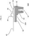
- the step (b) of providing a first power semiconductor module 100 comprises providing a preliminary first power semiconductor module 100' as shown in Fig. 3 .
- the preliminary first power semiconductor module 100' includes all features of the first power semiconductor module 100 as described above with reference to Fig. 2 .
- it includes the first base plate 30, the cooling extensions 37 protruding from the second main side 33 of the first base plate 30, the substrate 42 located on the first main side of the base plate 30, the at least one first die 40 and the lead frame 43 which are located on the substrate 42 and the at least one bonding wire 44 connecting the at least one die 40 with the lead frame 43.
- the first base plate 30 has the first step 35A on the second main side 33 along the circumferential edge of the first base plate 30 to form the first recess 35 along the circumferential edge of the first base plate 30.
- the first step 35A and the first recess 35 may be formed in a same manufacturing step together with the cooling protrusions 37 by forging. In this case no additional manufacturing step is required for forming the first step 35A and the recess 35 in the first base plate 30.
- the step (b) of providing the first power semiconductor module 100 comprises a step of molding an encapsulation 50, wherein the encapsulation 50 encapsulates the first main side 32 and the circumferential side surface 34 of the first base plate 30 such that a bottom surface of the encapsulation 50 is flush with the first base plate 30 at the circumferential edge of the first base plate 30.
- a bottom mold 70 and a top mold 80 is used, wherein the bottom mold 80 has a first flat surface 70A which is brought into contact with a second flat surface of the first recess 35 acting as a sealing surface during the molding step.
- the terminals of lead frame 43 are provided in the splitting plane between top mold 80 and the bottom mold 70 as shown in Fig. 4 .
- transfer molding or any other suitable molding or casting technique known to a person skilled in the art may be used as a molding or casting technique for molding or casting the encapsulation 50.
- step (c) of providing the second semiconductor module 200 comprises similar method steps and features as the step (b) described above. Accordingly, a description thereof will not be repeated but it is referred to the above description of step (b).
- step (d) of attaching the first power semiconductor module 100 to the frame 20 the first power semiconductor module 100 provided in step (b) is inserted with its cooling extensions 37 and part of the first base plate 30 into the first opening 23 such that the first portion 21 of the plate portion 22 is received in the first recess 35 as shown in any one of Figs. 5A to 5C . Then the first portion 21 is fixed to the first base plate 30 by welding or another bonding technique such as gluing or soldering. If the first base plate 30 is made of AlSiC an aluminium rich portion (which has exemplarily a thickness of 5 mm) may be integrated in the first base plate 30 where the welding connection is to be formed. In the embodiment illustrated in Fig.
- the first portion 21 is fixed to the first base plate 30 by laser welding.
- the laser beam 90 used for the laser welding is indicated as an arrow in Fig. 5A .
- the laser beam 90 is directed to an area at the gap between the step 35A and a lateral edge portion of the first portion 21 to form a butt weld connection between the first portion 21 and the first base plate 30.
- Fixing the first portion 21 to the first base plate by a butt weld connection has the advantage that it closes the gap between the step 35A and a lateral edge of the first portion 21 to provide a smooth surface for a wall of the cooling channel 65.
- the first portion 21 may be fixed to the first plate 30 by welding in another area than at the gap between the step 35A and a lateral edge of the first portion 21.
- welding could be performed also by laser welding through the first portion 21 or by a friction stir welding technique illustrated in Fig. 5B which shows a friction stir welding device 92.
- the first portion may be fixed to the first plate portion by a bonding technique as illustrated in Fig. 5C which shows a bonding layer 94.
- the bonding layer 94 may be made of a solder or glue, for example.
- step (e) Attaching the second power semiconductor module 200 to the frame 20 in step (e) is performed in the same manner as attaching the first power semiconductor module 100 to the frame 20 in step (d). Accordingly, a description thereof will not be repeated but it is referred to the above description of step (d) with reference to Figs. 5A to 5B .
- a bottom wall of a fluid channel 65 is formed to close the fluid channel 65 as shown in Fig. 1C .
- the electric power converter device 1 was described with two power semiconductor modules 100 and 200.
- the electric power converter device may alternatively include only one power semiconductor module or may alternatively include more than two power semiconductor modules.
- the invention may be applied to a two-level traction inverter for electric vehicles comprising six functional power semiconductor switches implemented as six power semiconductor modules.
- Such two-level traction inverter may exemplarily include three power-semiconductor modules, each containing two functional switches.
- the first and the second power semiconductor modules have been described to be substantially identical.
- the electric power converter includes plural power semiconductor modules these power semiconductor modules must not necessarily be identical but can be different from each other.
- these plural power semiconductor modules may have different dimensions.
- the side wall portion 24 was described as a part of the frame 20. However, the side wall portion 24 may also be a part of the cooler cover 60.
- the bottom surface 21A of the first portion 21 is flush with the second main side 33 of the first base plate 30 adjacent to the first step 35A.
- the bottom surface 21A of the first portion 21 is not necessarily flush with the second main side 33 of the first base plate 30 adjacent to the first step 35A.
- the depth of the first recess 35 is not necessarily the same as the thickness of the first portion 21 of the frame 20.
- molding or casting the encapsulation 50 was performed individually for each power semiconductor module before attaching the first and the second power semiconductor module 100, 200 to the frame 20. This has the advantage that the power semiconductor modules may be tested prior to integration with the frame 20. However, it would also be possible to form the encapsulation only after attaching the power semiconductor module(s) to the frame 20.
Landscapes
- Engineering & Computer Science (AREA)
- Microelectronics & Electronic Packaging (AREA)
- Physics & Mathematics (AREA)
- Thermal Sciences (AREA)
- Cooling Or The Like Of Semiconductors Or Solid State Devices (AREA)
- Inverter Devices (AREA)
Abstract
Description
- The present invention relates to an electric power converter device according to the preamble of claim 1.
- Direct water-glycol cooling of power semiconductor modules included in the electric power converters is common for use in harsh operating conditions. This is due to superior performance of direct cooling. Direct cooling means that a base plate of the power semiconductor module is in direct contact with the cooling fluid and contains a surface extension, typically in the form of pins.
- In a known electric converter, the substrate(s) of one or more power semiconductor devices is (are) placed on a common baseplate and a top side frame is screwed and glued to the top side of the baseplate. Resin is then potted into the frame for encapsulation of the one or more power semiconductor devices in one power semiconductor module. In order to prevent any leakage issues of cooling water and to avoid extensive use of screws, there is also a trend away from the open pin-fin base plate (which has to be sealed at a bottom side of the base plate by a screwed O-ring connection) approaches towards to a closed metal cooler being integrated with the power semiconductor module.
- Transfer-molded and sintered packages of power modules have become an interesting alternative to the traditional approach for encapsulation of power semiconductor devices by potting as described above. Sintering and mold compound encapsulation can significantly increase the cycle reliability of the power module. In addition, the module sintering in one step and the transfer molding approach can significantly reduce the manufacturing costs and the bill of material of the module.
- In the electric power semiconductor modules the transfer of heat from the base plate and the pins to the cooling fluid is most critical for the performance of the direct cooling. Also, much space is required by the known designs of an electric power converter with direct cooling.
- Some electrical power converters require plural power semiconductor devices. For example in two-level three-phase traction inverters for electric vehicles, six functional semiconductor switches are needed. Therein the six functional semiconductor switches require at least six semiconductor devices (chips), but may require even more semiconductor devices since several (typically 3 to 10) devices are parallel-connected per functional semiconductor switch.
- There are significant drawbacks when integrating plural power semiconductor devices within one molded and sintered module on a single common base plate. Molding across a large area is challenging because curing of the epoxy material during compound transfer limits the possible length of a molding channel, the mold compound loading volume in commercial equipment is limited, and the mismatch of the coefficient of thermal expansion (CTE) between a large area mold compound and a cooler or baseplate can lead to warpage and stresses that might impact the mechanical integrity and result in mold compound delamination. Moreover, one-step sintering of a power semiconductor module comprising plural power semiconductor devices is economically very risky, since the plural power semiconductor devices cannot be tested prior to assembly. While substrates can be fully assembled with wire bonds when heading for successive substrate soldering, substrates for sintering cannot be wire bonded and tested prior to sintering, since the sintering approach requires a strong pressure on the substrates (typically applied mechanically with a rubber stamp) that would destroy the wire bonding.
- In a known electric power converter comprising plural power semiconductor devices it may therefore be preferable to integrate the plural power semiconductor devices in plural molded or sintered power modules in a compact configuration with a single closed cooler. However integrating plural molded or sintered power modules into a compact configuration with a closed cooler requires that a fluid channel (or containment) is created around the pins of the base plate of each power module, and that the channels must be fluidly connected. This is a challenge, since the connections must be robust and tight. Also, as indicated above the design should be space saving and cheap.
- From
DE 10 2009 045 063 A1 there is known a power semiconductor module system comprising a power semiconductor module and an add-on heat sink element. The power semiconductor module includes a substrate, a semiconductor die on a front side of the substrate and a heat sink made of resin, which is molded to a back side of the substrate. The add-on heat sink element is attached to the power semiconductor module such that a channel for a cooling fluid is formed, wherein the cooling fluid in the channel is in direct contact with the heat sink. It is described to attach the add-on heat sink element to the power semiconductor module by a screw joint or by bonding. For sealing purposes it is described to use an O-ring provided in a groove in the heat sink or in the add-on heat sink element. A pressure drop in in the cooling fluid is relatively high in this prior art power semiconductor module system. - From
JP 5659935 B2 - In view of the above disadvantages in the prior art it is an object of the invention to provide an electric power converter device which overcomes the above disadvantages in the prior art. In particular it is an object of the invention to provide an electric power converter integrating a frame for a cooler (i.e. a cooler frame) in a space-saving manner and in such manner that a cooling efficiency can be improved.
- The object is attained by an electric power converter device according to claim 1. Further developments of the invention are specified in the dependent claims.
- The electric power converter device of the invention comprises a first power semiconductor module and a frame for a closed cooler. The first power semiconductor module includes a first base plate and at least one first die. The first base plate has a first main side, a second main side opposite the first main side and a lateral side surface extending along a circumferential edge of the first base plate and connecting the first and the second main side. The at least one first die is located on the first main side of the first base plate. The frame is attached to the second main side of the first base plate. The first base plate has a first step on the second main side along the circumferential edge of the first base plate to form a first recess along the circumferential edge of the first base plate, in which first recess a first portion of the frame is received.
- With the first recess along the circumferential edge of the first base plate, in which the first portion of the frame is received, the frame for the closed cooler can be attached to the base plate in a space-saving manner because the first portion of the frame does not add to the total thickness of the electric power converter device. Furthermore, by providing the recess in which the first portion of the frame is received, the lower side of the first portion of the frame and that portion of the second main side of the first base plate along which a cooling fluid flows in operation of the electric power converter can be brought closer to each other in a direction perpendicular to the second main side of the first base plate, so that the cooling fluid can flow more smoothly along the lower side of the first portion of the frame and the second main side of the base plate. This results in a lower pressure drop in the cooling fluid and thereby in an improved cooling efficiency.
- In an exemplary embodiment the first portion of the frame is a flange portion that is received in the first recess such that a bottom surface of the flange portion is flush with the second main side of the first base plate adjacent to the first step. In this exemplary embodiment a surface which includes the bottom surface of the flange portion and the second main side adjacent to the first step has no step but provides a smooth surface without a step, so that a resistance for the flow of a cooling fluid flowing along this surface can be minimized. This results in a low pressure drop in the cooling fluid and thereby in an improved cooling efficiency.
- In an exemplary embodiment the first portion of the frame is fixed to the first base plate by a welding connection.
- In an exemplary embodiment the first base plate has a reduced first thickness along its circumferential edge compared to a second thickness of the first base plate in a central area of the first base plate which central area is laterally surrounded by the first step. An advantage of the base plate having a lower first thickness along the circumferential edge due to the first step on the second main side is the possible reduction of use of material for the base plate (resulting in lower weight and cost) if the first step is directly shaped when forging the base plate. The base plate may be thick only in the area below the at least one die. In this area, the relatively high second thickness is needed for heat spreading. In the more peripheral regions, there may be no die and hence much lower losses, making heat spreading much less important. The first thickness of the first base plate is reduced there because of the first step.
- In an exemplary embodiment the electric power converter device comprises a plurality of cooling extensions protruding from the second main side of the first base plate in a central area of the first base plate which central area is laterally surrounded by the first step. In this exemplary embodiment the cooling efficiency can be improved. Due to the first recess the cooling extensions close to the frame are cooled more efficiently compared to a case where the first portion would be attached to a base plate having no recess. The cooling extensions can be manufactured together with the first recess in a single manufacturing step by forging.
- In an exemplary embodiment the frame has a plate portion that comprises an opening, wherein an edge of the plate portion directly adjacent to the opening and surrounding the opening is the first portion of the frame. In this exemplary embodiment the plate portion forms a flat wall portion of a channel in the closed cooler.
- In an exemplary embodiment the plate portion has a third thickness which is the same as a depth of the first recess in the first base plate. In such exemplary embodiment a lower side of the plate portion is flush with the second main side of the first base plate.
- In an exemplary embodiment the electric power converter device comprises a molded encapsulation, which encapsulates the first main side and the lateral side surface of the first base plate such that a bottom surface of the encapsulation is flush with the first base plate at the circumferential edge of the first base plate on the second main side. In this exemplary embodiment integration of the frame is facilitated, because a surface of the frame facing towards encapsulation and towards the first recess can be a flat surface. Moreover, forming the encapsulation is facilitated because the second main side surface in the first recess can be used as an abutment or sealing face for a mold for forming the encapsulation by molding.
- In an exemplary embodiment the first base plate is made of copper (Cu), or aluminum (Al), or aluminum silicon carbide (AlSiC), or a combination of copper (Cu) and aluminum (Al). Such materials have a high thermal conductivity and high durability to withstand harsh conditions and direct contact with the cooling liquid during operation of the device. In an exemplary embodiment the electric power converter device comprises a cooler cover attached to the frame at a side opposite to the first base plate to form a bottom wall portion of a fluid channel in the closed cooler.
- In an exemplary embodiment the electric power converter device comprises at least one second power semiconductor module, the second power semiconductor module including: a second base plate having a third main side and a fourth main side opposite the third main side; and at least one second die located on the third main side of the second base plate, wherein the frame is attached to the fourth main side of the second base plate, and wherein the second base plate has a second step on the fourth main side along a circumferential edge of the second base plate to form a second recess along the circumferential edge of the second base plate in which a second portion of the frame is received. In this exemplary embodiment integrating the first and the second power semiconductor module with one single closed cooler is facilitated. A fluid channel (or containment) is created at the first and the second base plate, and the channels are fluidly connected in a robust and tight manner. Also, the design allows to integrate plural power semiconductor modules in a space-saving and relatively cheap manner. The second semiconductor power module may have the same features and may be integrated with the frame in the same way as described above for the first power semiconductor module, i.e. plural semiconductor power modules may have the same features and may be attached to the frame in the same way as described above for the first power semiconductor module.
- In an exemplary embodiment the electric power converter device of the invention may be manufactured by a method comprising the following steps: providing a frame for a closed cooler; providing a first power semiconductor module, the first power semiconductor module including a first base plate having a first main side, a second main side opposite the first main side and a lateral side surface extending along a circumferential edge of the first base plate and connecting the first and the second main side; and at least one first die located on the first main side of the first base plate, wherein the first base plate has a first step on the second main side along the circumferential edge of the first base plate to form a first recess along the circumferential edge of the first base plate; and attaching the first power semiconductor module to the frame such that a first portion of the frame is received in the first recess and fixed to the first base plate.
- With the first recess along the circumferential edge of the first base plate, in which the first portion of the frame is received, the frame for the closed cooler can be attached to the base plate in a space-saving manner, a pressure drop in a cooling fluid is reduced and cooling efficiency can be improved as discussed above.
- The step of providing the first power semiconductor module may comprise molding an encapsulation, wherein the encapsulation encapsulates the first main side and the circumferential side surface of the first base plate such that a bottom surface of the encapsulation is flush with the first base plate at the circumferential edge of the first base plate; and wherein a bottom mold and a top mold is used, the bottom mold having a first flat surface which is brought into contact with a second flat surface of the first recess acting as a sealing surface during the molding step. Using the second flat surface of the first recess as a sealing surface results in a reliable sealing of the mold to form the encapsulation in a reliable manner without any compound flash or bleed at the sealing surface.
- In an exemplary embodiment the frame has a plate portion that comprises an opening, wherein an edge portion of the plate portion, which is directly adjacent to the opening and which surrounds the opening, is the first portion of the frame, and wherein in the step of attaching the first power semiconductor module to the frame the first portion is fixed to the first base plate by welding or bonding. Providing the frame with a plate portion having an opening into which the first semiconductor module is inserted, such that the first portion of the frame is received in the first recess, facilitates integration of the first semiconductor module with the frame.
- An exemplary embodiment comprises the additional steps of providing a second power semiconductor module, the second power semiconductor module including a second base plate having a third main side, a fourth main side opposite the third main side and a lateral side surface extending along a circumferential edge of the second base plate and connecting the third and the fourth main side; and at least one second die located on the third main side of the second base plate, wherein the second base plate has a second step on the fourth main side along the circumferential edge of the second base plate to form a second recess along the circumferential edge of the second base plate; and attaching the second power semiconductor module to the frame such that a second portion of the frame is received in the second recess and fixed to the second base plate. In this exemplary embodiment plural power semiconductor modules can efficiently be integrated with a single frame in a reliable manner. By providing the first and the second power semiconductor modules as separate parts, these power semiconductor modules can be tested prior to integration with the single frame. This results in a high yield in manufacturing the electric power converter.
- Detailed embodiments of the invention will be explained below with reference to the accompanying figures, in which:
- Fig. 1A
- shows an electric power converter device according to an embodiment in a cross-section taken along line A-A' in
Fig. 1D ; - Fig. 1B
- shows the electric power converter device of
Fig. 1A in a cross-section taken along line C-C' inFig. 1D ; - Fig. 1C
- shows the electric power converter device of
Fig. 1A in a cross-section taken along line B-B' inFig. 1D ; - Fig. 1D
- shows a top view of the electric power converter device of
Fig. 1A ; - Fig. 2
- shows an enlarged partial view of the cross-section shown in
Fig. 1A ; - Fig. 3
- shows an enlarged partial view of a power semiconductor module in cross-section illustrating a step of providing a power semiconductor module in a method for manufacturing the electric power converter device of
Fig. 1A ; - Fig. 4
- shows an enlarged partial view of the power semiconductor module in cross-section illustrating a step of forming an encapsulation in a method for manufacturing the electric power converter device of
Fig. 1A ; - Fig. 5A
- shows an enlarged partial view of an electric power converter device in cross-section illustrating a step of attaching a frame to a power semiconductor module in a method for manufacturing the electric power converter device of
Fig. 1A ; - Fig. 5B
- shows an enlarged partial view of an electric power converter device in cross-section illustrating a step of attaching a frame to a power semiconductor module in a method for manufacturing the electric power converter device of
Fig. 1A according to a modified embodiment; and - Fig. 5C
- shows an enlarged partial view of an electric power converter device in cross-section illustrating a step of attaching a frame to a power semiconductor module in a method for manufacturing the electric power converter device of
Fig. 1A according to another modified embodiment. - The reference signs used in the figures and their meanings are summarized in the list of reference signs. Generally, similar elements have the same reference signs throughout the specification. The described embodiments are meant as examples and shall not limit the scope of the invention.
- In the following an electric power converter device 1 according to an embodiment of the invention is described with reference to
Figs. 1A, 1B ,1C, 1D and2 .Fig. 1D shows a top view of the electric power converter device 1.Fig. 1A shows the electric power converter device 1 in a cross-section taken along line A-A' inFig. 1D ,Fig. 1B shows the electric power converter device 1 in a cross-section taken along line C-C' inFig. 1D and Fig. 1C shows the electric power converter device 1 in a cross-section taken along line B-B' inFig. 1D .Fig. 2 shows an enlarged partial view of section S in the cross-section shown inFig. 1A . - As can be seen best from
Fig. 1C the electric power converter device 1 according to the embodiment comprises a firstpower semiconductor module 100, a secondpower semiconductor module 200, aframe 20 for a closed cooler, and acooler cover 60. The firstpower semiconductor module 100, which is illustrated in more detail in the cross-section shown inFig. 1A and the enlarged partial view of section S inFig. 2 , includes afirst base plate 30 and at least onefirst die 40. Thebase plate 30 has a firstmain side 32, a secondmain side 33 opposite to the firstmain side 32 and alateral side surface 34, which extends along a circumferential edge of thefirst base plate 30 and which connects the firstmain side 32 and the secondmain side 33. The at least one die 40 is located on the firstmain side 32 of thefirst base plate 30. - The
first base plate 30 has afirst step 35A on the secondmain side 33 along the circumferential edge of thefirst base plate 30 to form afirst recess 35 along the circumferential edge of thefirst base plate 30. In the present embodimentfirst base plate 30 has a reduced first thickness d1 along its circumferential edge compared to a second thickness d2 of thefirst base plate 30 in a central area of thefirst base plate 30, which central area is laterally surrounded by thefirst step 35A. Accordingly, in the present embodiment the height of thefirst step 35A is given by the difference d2-d1 between the second thickness d2and the first thickness d1. - The
frame 20 has aplate portion 22 and aside wall portion 24 extending in vertical direction perpendicular to the firstmain side 32 from a circumferential edge of theplate portion 22. As shown inFig. 1D theplate portion 22 comprises afirst opening 23 and a second opening 23'. An edge portion of theplate portion 22, which is directly adjacent to thefirst opening 23 and which surrounds thefirst opening 23, is afirst portion 21 of theframe 20, which is attached to thefirst base plate 30 of the firstpower semiconductor module 100 as described in more detail below. Likewise an edge portion of theplate portion 22, which is directly adjacent to the second opening 23' and which surrounds the second opening 23', is a second portion 21' of theframe 20, which is attached to asecond base plate 30 of the secondpower semiconductor module 200 as described in more detail below. - A thickness d3 of the
first portion 21 of theplate portion 22 in a direction perpendicular to the firstmain side 32 is substantially the same as a depth of thefirst recess 35, which is defined by the height d2-d1 of the first step 35A.Thefirst portion 21 of theframe 20, which is a flange portion, is received in thefirst recess 35 such that abottom surface 21A of thefirst portion 21 is substantially flush with the secondmain side 33 of thefirst base plate 30 adjacent to thefirst step 35A. In an exemplary embodiment, thewhole plate portion 22 may have a constant thickness d3. - The
frame 20 is attached to the secondmain side 33 of thefirst base plate 30 by thefirst portion 21 of theframe 20 being fixed to thefirst base plate 30 for example by a welding connection, by a bonding connection or by any other suitable connection. - A plurality of
cooling extensions 37 protrude from the secondmain side 33 of thefirst base plate 30 in the central area of thefirst base plate 30 which central area is laterally surrounded by thefirst step 35A. Therein, a lateral direction is any direction parallel to the firstmain side 32. - The
first base plate 30 and thecooling extensions 37 are made from any suitable material having a high thermal conductivity. Exemplarily, thefirst base plate 30 may be made of copper (Cu) or aluminum (Al) or aluminum silicon carbide (AlSiC) or a combination of copper and aluminum. For example, thefirst base plate 30 may be a two-layered base plate which has a top layer made from Cu and a bottom layer made from Al. The cooling extensions extending from the bottom layer may also be made from Al. - As illustrated in the enlarged partial view shown in
Fig. 2 , the firstpower semiconductor module 100 includes alead frame 43 which is located together with the at least one die 40 on asubstrate 42. An electrical connection between thelead frame 43 and the at least one die 40 may be provided by at least onebonding wire 44, for example. The substrate may be a direct bonded copper (DBC) substrate. - A molded
encapsulation 50 encapsulates the firstmain side 32 and thelateral side surface 34 of thefirst base plate 30. As a result the at least onefirst die 40, thesubstrate 42 and the at least onebonding wire 44 is encapsulated by theencapsulation 50. A portion of thelead frame 43 which acts as a terminal of thepower semiconductor module 100, protrudes from a lateral side of theencapsulation 50. A bottom surface of theencapsulation 50 is substantially flush with thefirst base plate 30 at the circumferential edge of thebase plate 30 on the secondmain side 33. - The
cooler cover 60 is attached to theframe 20 at a side opposite to thefirst base plate 30 to form a bottom wall portion of afluid channel 65 in the closed cooler. During operation of the electric power converter device 1 a flow of a cooling fluid F through thefluid channel 65 takes places as indicated by arrows inFig. 1C . - A first cross-section of the second
power semiconductor module 200 along line Fig. C-C' inFig. 1D is shown inFig. 1B and a second cross-section of the secondpower semiconductor module 200 along line B-B' inFig. 1D is shown inFig. 1C . In the present embodiment the secondpower semiconductor module 200 is basically identical to the firstpower semiconductor module 100. Accordingly, for details it is referred to the above discussion of the firstpower semiconductor module 100. Similar to the firstpower semiconductor module 100, the secondpower semiconductor module 200 includes a second base plate 30' having a third main side 32' and a fourth main side 33' opposite to the third main side 32', and at least one second die (not shown in the figures) located on the third main side (32') of the second base plate (30'). - The
frame 20 is attached to the fourth main side 33' of the second base plate 30' in basically the same manner as theframe 20 is attached to the secondmain side 33 of thefirst base plate 30. In particular, the second base plate 30' has a second step on the fourth main side 33' along a circumferential edge of the second base plate 30' to form a second recess 35' along the circumferential edge of the second base plate 30' in which the second portion 21' of theframe 20 is received as shown inFig. 1B , for example. The second recess 35' may have the same depth as the depth d2-d1 of thefirst recess 35 in thefirst base plate 30 of the firstpower semiconductor module 100. - In an exemplary embodiment, the above described
power semiconductor modules - Next a method for manufacturing the electric power converter device according to the above embodiment shown in
Figs. 1A to 2 will be described. The method comprises in general the following steps: - (a) providing the
frame 20 for a closed cooler, - (b) providing the first
power semiconductor module 100, - (c) providing the second
power semiconductor module 200, - (d) attaching the first
power semiconductor module 100 to theframe 20, - (e) attaching the second
power semiconductor module 200 to theframe 20, and - (f) attaching the
cooler cover 60 to theframe 20. - In step (a) of providing the
frame 20 for a closed cooler, theframe 20 described above with reference toFig. 1D and2 is provided. Accordingly, a description thereof will not be repeated but it is referred to the above description of theframe 20. - The step (b) of providing a first
power semiconductor module 100 comprises providing a preliminary first power semiconductor module 100' as shown inFig. 3 . The preliminary first power semiconductor module 100' includes all features of the firstpower semiconductor module 100 as described above with reference toFig. 2 . In particular, it includes thefirst base plate 30, thecooling extensions 37 protruding from the secondmain side 33 of thefirst base plate 30, thesubstrate 42 located on the first main side of thebase plate 30, the at least onefirst die 40 and thelead frame 43 which are located on thesubstrate 42 and the at least onebonding wire 44 connecting the at least one die 40 with thelead frame 43. Thefirst base plate 30 has thefirst step 35A on the secondmain side 33 along the circumferential edge of thefirst base plate 30 to form thefirst recess 35 along the circumferential edge of thefirst base plate 30. - In the above step (b) the
first step 35A and thefirst recess 35 may be formed in a same manufacturing step together with the coolingprotrusions 37 by forging. In this case no additional manufacturing step is required for forming thefirst step 35A and therecess 35 in thefirst base plate 30. - Furthermore the step (b) of providing the first
power semiconductor module 100 comprises a step of molding anencapsulation 50, wherein theencapsulation 50 encapsulates the firstmain side 32 and thecircumferential side surface 34 of thefirst base plate 30 such that a bottom surface of theencapsulation 50 is flush with thefirst base plate 30 at the circumferential edge of thefirst base plate 30. During molding abottom mold 70 and atop mold 80 is used, wherein thebottom mold 80 has a firstflat surface 70A which is brought into contact with a second flat surface of thefirst recess 35 acting as a sealing surface during the molding step. By providing the flat sealing surface in therecess 35 at the secondmain side 33 it is ensured that the molded material cannot be formed on the coolingprotrusions 37, but this results in a rim of molded material around thefirst base plate 30 as shown inFigs. 5A to 5C . The terminals oflead frame 43 are provided in the splitting plane betweentop mold 80 and thebottom mold 70 as shown inFig. 4 . Exemplarily, transfer molding or any other suitable molding or casting technique known to a person skilled in the art may be used as a molding or casting technique for molding or casting theencapsulation 50. - The step (c) of providing the
second semiconductor module 200 comprises similar method steps and features as the step (b) described above. Accordingly, a description thereof will not be repeated but it is referred to the above description of step (b). - In the step (d) of attaching the first
power semiconductor module 100 to theframe 20 the firstpower semiconductor module 100 provided in step (b) is inserted with itscooling extensions 37 and part of thefirst base plate 30 into thefirst opening 23 such that thefirst portion 21 of theplate portion 22 is received in thefirst recess 35 as shown in any one ofFigs. 5A to 5C . Then thefirst portion 21 is fixed to thefirst base plate 30 by welding or another bonding technique such as gluing or soldering. If thefirst base plate 30 is made of AlSiC an aluminium rich portion (which has exemplarily a thickness of 5 mm) may be integrated in thefirst base plate 30 where the welding connection is to be formed. In the embodiment illustrated inFig. 5A thefirst portion 21 is fixed to thefirst base plate 30 by laser welding. Thelaser beam 90 used for the laser welding is indicated as an arrow inFig. 5A . In particular, thelaser beam 90 is directed to an area at the gap between thestep 35A and a lateral edge portion of thefirst portion 21 to form a butt weld connection between thefirst portion 21 and thefirst base plate 30. Fixing thefirst portion 21 to the first base plate by a butt weld connection has the advantage that it closes the gap between thestep 35A and a lateral edge of thefirst portion 21 to provide a smooth surface for a wall of the coolingchannel 65. It is to be noted that due to the rim portion of molded material around the first base plate 30 a butt weld would not be possible without therecess 35 but is made possible only due to thefirst portion 21 being received in thefirst recess 35. Alternatively, thefirst portion 21 may be fixed to thefirst plate 30 by welding in another area than at the gap between thestep 35A and a lateral edge of thefirst portion 21. For example such welding could be performed also by laser welding through thefirst portion 21 or by a friction stir welding technique illustrated inFig. 5B which shows a frictionstir welding device 92. Alternatively, the first portion may be fixed to the first plate portion by a bonding technique as illustrated inFig. 5C which shows abonding layer 94. Thebonding layer 94 may be made of a solder or glue, for example. - Attaching the second
power semiconductor module 200 to theframe 20 in step (e) is performed in the same manner as attaching the firstpower semiconductor module 100 to theframe 20 in step (d). Accordingly, a description thereof will not be repeated but it is referred to the above description of step (d) with reference toFigs. 5A to 5B . - By attaching the
cooler cover 60 to the frame 20 a bottom wall of afluid channel 65 is formed to close thefluid channel 65 as shown inFig. 1C . - It will be apparent for persons skilled in the art that modifications of the above described embodiment are possible without departing from the scope of the invention as defined by the appended claims.
- In the above embodiments the electric power converter device 1 was described with two
power semiconductor modules - Also, in the above embodiments the first and the second power semiconductor modules have been described to be substantially identical. However, in case that the electric power converter includes plural power semiconductor modules these power semiconductor modules must not necessarily be identical but can be different from each other. In particular, these plural power semiconductor modules may have different dimensions.
- In the above embodiments the
side wall portion 24 was described as a part of theframe 20. However, theside wall portion 24 may also be a part of thecooler cover 60. - In the above described embodiment of the electric power converter device 1 the
bottom surface 21A of thefirst portion 21 is flush with the secondmain side 33 of thefirst base plate 30 adjacent to thefirst step 35A. However, thebottom surface 21A of thefirst portion 21 is not necessarily flush with the secondmain side 33 of thefirst base plate 30 adjacent to thefirst step 35A. Likewise, the depth of thefirst recess 35 is not necessarily the same as the thickness of thefirst portion 21 of theframe 20. - In the above embodiment for manufacturing the electric power converter device of the invention molding or casting the
encapsulation 50 was performed individually for each power semiconductor module before attaching the first and the secondpower semiconductor module frame 20. This has the advantage that the power semiconductor modules may be tested prior to integration with theframe 20. However, it would also be possible to form the encapsulation only after attaching the power semiconductor module(s) to theframe 20. - It should be noted that the term "comprising" does not exclude other elements or steps and that the indefinite article "a" or "an" does not exclude the plural. Also elements described in association with different embodiments may be combined.
-
- 1
- electric power converter device
- 100
- first power semiconductor module
- 100'
- preliminary first power semiconductor module
- 20, 20'
- frame
- 200
- second power semiconductor module
- 21A
- bottom surface
- 21
- first portion
- 21'
- second portion
- 22
- plate portion
- 23
- first opening
- 23'
- second opening
- 24
- side wall portion
- 30
- first base plate
- 30'
- second base plate
- 32
- first main side
- 32'
- third main side
- 33
- second main side
- 33'
- fourth main side
- 34, 34'
- lateral side surface
- 35
- first recess
- 35'
- second recess
- 35A
- first step
- 37
- cooling extension
- 40
- first die
- 42
- substrate
- 44
- bonding wire
- 50
- encapsulation
- 60
- cooler cover
- 65
- fluid channel
- 70
- bottom mold
- 70A
- first flat surface
- 80
- top mold
- d1
- first thickness
- d2
- second thickness
- d3
- third thickness
Claims (15)
- An electric power converter device, comprising:a first power semiconductor module (100); anda frame (20) for a closed cooler,the first power semiconductor module (100) includinga first base plate (30) having a first main side (32), a second main side (33) opposite the first main side (32) and a lateral side surface (34) extending along a circumferential edge of the first base plate (30) and connecting the first main side (32) and the second main side (33); andat least one first die (40) located on the first main side (32) of the first base plate (30),wherein the frame (20) is attached to the second main side (33) of the first base plate (30),characterized in that the first base plate (30) has a first step (35A) on the second main side (33) along the circumferential edge of the first base plate (30) to form a first recess (35) along the circumferential edge of the first base plate (30), in which first recess (35) a first portion (21) of the frame (20) is received.
- The electric power converter device according to claim 1, wherein the first portion (21) of the frame (20) is a flange portion that is received in the first recess (35) such that a bottom surface (21A) of the flange portion is flush with the second main side (33) of the first base plate (30) adjacent to the first step (35A).
- The electric power converter device according to claim 1 or 2, wherein the first portion (21) of the frame (20) is fixed to the first base plate (30) by a welding connection.
- The electric power converter device according to any one of the preceding claims, wherein the first base plate (30) has a reduced first thickness (d1) along its circumferential edge compared to a second thickness (d2) of the first base plate (30) in a central area of the first base plate (30) which central area is laterally surrounded by the first step (35A).
- The electric power converter device according to any one of the preceding claims, comprising a plurality of cooling extensions (37) protruding from the second main side (33) of the first base plate (30) in a central area of the first base plate (30) which central area is laterally surrounded by the first step (35A).
- The electric power converter device according to any one of the preceding claims, wherein the frame (20) has a plate portion (22) that comprises an opening (23) and wherein an edge portion of the plate portion (22), which is directly adjacent to the opening (23) and which surrounds the opening (23), is the first portion (21) of the frame (20).
- The electric power converter device according to claim 6, wherein the plate portion (22) has a third thickness (d3) which is the same as a depth of the first recess (35) in the first base plate (30).
- The electric power converter device according to any one of the preceding claims, comprising a molded encapsulation (50), which encapsulates the first main side (32) and the lateral side surface (34) of the first base plate (30) such that a bottom surface of the encapsulation (50) is flush with the first base plate (30) at the circumferential edge of the base plate (30) on the second main side (33).
- The electric power converter device according to any one of the preceding claims, wherein the first base plate (30) is made of copper (Cu), or aluminum (Al), or aluminum silicon carbide (AlSiC), or a combination of copper (Cu) and aluminum (Al).
- The electric power converter device according to any one of the preceding claims, comprising a cooler cover (60) attached to the frame (20) at a side opposite to the first base plate (30) to form a bottom wall portion of a fluid channel (65) in the closed cooler.
- The electric power converter device according to any one of the preceding claims, comprising at least one second power semiconductor module (200),
the second power semiconductor module (200) including:a second base plate (30') having a third main side (32') and a fourth main side (33') opposite the third main side (32'); andat least one second die located on the third main side (32') of the second base plate (30'),wherein the frame (20) is attached to the fourth main side (33') of the second base plate (30'), andwherein the second base plate (30') has a second step on the fourth main side (33') along a circumferential edge of the second base plate (30') to form a second recess along the circumferential edge of the second base plate (30') in which a second portion (21') of the frame (20) is received. - A method for manufacturing the electric power converter device according to any one of the preceding claims, the method comprising the following steps:providing a frame (20) for a closed cooler;providing a first power semiconductor module (100), the first power semiconductor module (100) including a first base plate (30) having a first main side (32), a second main side (33) opposite the first main side (32) and a lateral side surface (34) extending along a circumferential edge of the first base plate (30) and connecting the first main side (32) and the second main side (33); and at least one first die (40) located on the first main side (32) of the first base plate (30), wherein the first base plate (30) has a first step (35A) on the second main side (33) along the circumferential edge of the first base plate (30) to form a first recess along the circumferential edge of the first base plate (30); andattaching the first power semiconductor module (100) to the frame (20) such that a first portion (21) of the frame (20) is received in the first recess (35) and fixed to the first base plate (30).
- The method according to claim 12, wherein providing the first power semiconductor module (100) comprises molding an encapsulation (50), wherein the encapsulation (50) encapsulates the first main side (32) and the circumferential side surface (34) of the first base plate (30) such that a bottom surface of the encapsulation (50) is flush with the first base plate (30) at the circumferential edge of the first base plate (30) ; and wherein a bottom mold (70) and a top mold (80) is used, the bottom mold (80) having a first flat surface (70A) which is brought into contact with a second flat surface of the first recess (35) acting as a sealing surface during the molding step.
- The method according to claim 12 or 13, wherein the frame (20) has a plate portion (22) that comprises an opening (23), wherein an edge portion of the plate portion (22), which is directly adjacent to the opening (23) and which surrounds the opening (23), is the first portion (21) of the frame (20), and wherein in the step of attaching the first power semiconductor module (100) to the frame (20) the first portion (21) is fixed to the first base plate (30) by welding or bonding.
- The method according to any one of claims 12 to 14, comprising the following steps:providing a second power semiconductor module (200), the second power semiconductor module (200) including a second base plate (30') having a third main side (32'), a fourth main side (33') opposite the third main side (32') and a lateral side surface (34) extending along a circumferential edge of the second base plate (30') and connecting the third main side (32') and the fourth main side (33'); and at least one second die located on the third main side (32') of the second base plate (30'), wherein the second base plate (30') has a second step on the fourth main side (33') along the circumferential edge of the second base plate (30') to form a second recess (35') along the circumferential edge of the second base plate (30'); andattaching the second power semiconductor module (200) to the frame (20) such that a second portion (21') of the frame (20) is received in the second recess (35') and fixed to the second base plate (30').
Priority Applications (6)
| Application Number | Priority Date | Filing Date | Title |
|---|---|---|---|
| EP19160101.2A EP3703117B1 (en) | 2019-02-28 | 2019-02-28 | Electric power converter device with improved integration of cooler frame |
| CN202080016946.0A CN113544845A (en) | 2019-02-28 | 2020-02-25 | Power converter device with improved integrated cooler frame |
| JP2021551583A JP7573818B2 (en) | 2019-02-28 | 2020-02-25 | Power converter with improved cooler frame integration |
| EP20706730.7A EP3931867B1 (en) | 2019-02-28 | 2020-02-25 | Electric power converter device with improved integration of cooler frame |
| US17/434,546 US12016162B2 (en) | 2019-02-28 | 2020-02-25 | Electric power converter device with improved integration of cooler frame |
| PCT/EP2020/054828 WO2020173899A1 (en) | 2019-02-28 | 2020-02-25 | Electric power converter device with improved integration of cooler frame |
Applications Claiming Priority (1)
| Application Number | Priority Date | Filing Date | Title |
|---|---|---|---|
| EP19160101.2A EP3703117B1 (en) | 2019-02-28 | 2019-02-28 | Electric power converter device with improved integration of cooler frame |
Publications (2)
| Publication Number | Publication Date |
|---|---|
| EP3703117A1 true EP3703117A1 (en) | 2020-09-02 |
| EP3703117B1 EP3703117B1 (en) | 2022-11-23 |
Family
ID=65685134
Family Applications (2)
| Application Number | Title | Priority Date | Filing Date |
|---|---|---|---|
| EP19160101.2A Active EP3703117B1 (en) | 2019-02-28 | 2019-02-28 | Electric power converter device with improved integration of cooler frame |
| EP20706730.7A Active EP3931867B1 (en) | 2019-02-28 | 2020-02-25 | Electric power converter device with improved integration of cooler frame |
Family Applications After (1)
| Application Number | Title | Priority Date | Filing Date |
|---|---|---|---|
| EP20706730.7A Active EP3931867B1 (en) | 2019-02-28 | 2020-02-25 | Electric power converter device with improved integration of cooler frame |
Country Status (5)
| Country | Link |
|---|---|
| US (1) | US12016162B2 (en) |
| EP (2) | EP3703117B1 (en) |
| JP (1) | JP7573818B2 (en) |
| CN (1) | CN113544845A (en) |
| WO (1) | WO2020173899A1 (en) |
Cited By (5)
| Publication number | Priority date | Publication date | Assignee | Title |
|---|---|---|---|---|
| WO2022117663A1 (en) * | 2020-12-03 | 2022-06-09 | Hitachi Energy Switzerland Ag | Arrangement of a power semiconductor module and a cooler |
| EP4060724A1 (en) * | 2021-03-19 | 2022-09-21 | Hitachi Energy Switzerland AG | A power module comprising at least one semiconductor module, and a method for manufacturing a power module |
| EP4071802A1 (en) * | 2021-04-05 | 2022-10-12 | JMJ Korea Co., Ltd. | Cooling system where semiconductor component comprising semiconductor chip and cooling apparatus are joined |
| EP4184567A1 (en) * | 2021-11-18 | 2023-05-24 | Hitachi Energy Switzerland AG | Cooler unit, semiconductor device and method for manufacturing a cooler unit |
| WO2025242633A1 (en) * | 2024-05-22 | 2025-11-27 | Robert Bosch Gmbh | Electronic assembly |
Families Citing this family (3)
| Publication number | Priority date | Publication date | Assignee | Title |
|---|---|---|---|---|
| JP2022190987A (en) * | 2021-06-15 | 2022-12-27 | 株式会社フジクラ | cold plate |
| DE102022212458A1 (en) * | 2022-11-22 | 2024-05-23 | Magna powertrain gmbh & co kg | Power converter with directly cooled power module and method for manufacturing a power converter |
| KR20240149253A (en) * | 2023-04-05 | 2024-10-14 | 주식회사 엘엑스세미콘 | Power semiconductor module and power conversion device including the same |
Citations (8)
| Publication number | Priority date | Publication date | Assignee | Title |
|---|---|---|---|---|
| JP2010199494A (en) * | 2009-02-27 | 2010-09-09 | Mitsubishi Electric Corp | Semiconductor device and manufacturing method of the same |
| DE102009045063A1 (en) | 2009-09-28 | 2011-03-31 | Infineon Technologies Ag | Power semiconductor module, has power semiconductor chip arranged on substrate, and heat sink contacting substrate directly and made of plastic-based injection molding compound that exhibits specific heat conductivity |
| US20110304039A1 (en) * | 2010-06-15 | 2011-12-15 | Mitsubishi Electric Corporation | Semiconductor device |
| US20120235293A1 (en) * | 2011-03-15 | 2012-09-20 | Infineon Technologies Ag | Semiconductor device including a base plate |
| JP5659935B2 (en) | 2011-04-14 | 2015-01-28 | 三菱電機株式会社 | Semiconductor device |
| US20150097281A1 (en) * | 2013-10-03 | 2015-04-09 | Fuji Electric Co., Ltd. | Semiconductor device |
| US20150380338A1 (en) * | 2013-04-25 | 2015-12-31 | Fuji Electric Co., Ltd. | Semiconductor device |
| JP2016001766A (en) * | 2015-10-08 | 2016-01-07 | 三菱電機株式会社 | Semiconductor module |
Family Cites Families (13)
| Publication number | Priority date | Publication date | Assignee | Title |
|---|---|---|---|---|
| JP2003101277A (en) * | 2001-09-26 | 2003-04-04 | Toyota Motor Corp | Heating element cooling structure and method of manufacturing the same |
| JP2008270297A (en) | 2007-04-16 | 2008-11-06 | Sumitomo Electric Ind Ltd | Power unit and heat dissipation container |
| JP5171404B2 (en) | 2008-06-05 | 2013-03-27 | 三菱電機株式会社 | Resin mold type semiconductor module |
| US8237260B2 (en) * | 2008-11-26 | 2012-08-07 | Infineon Technologies Ag | Power semiconductor module with segmented base plate |
| JP5568026B2 (en) | 2011-01-20 | 2014-08-06 | トヨタ自動車株式会社 | Brazing method and brazing structure |
| JP2013030649A (en) | 2011-07-29 | 2013-02-07 | Mitsubishi Electric Corp | Semiconductor module and manufacturing method of the same |
| JP5567530B2 (en) * | 2011-08-19 | 2014-08-06 | 日立オートモティブシステムズ株式会社 | Friction stir welding structure and power semiconductor device |
| JP5955251B2 (en) | 2013-03-18 | 2016-07-20 | 三菱電機株式会社 | Power semiconductor module |
| JP5541393B2 (en) | 2013-06-05 | 2014-07-09 | 三菱電機株式会社 | Method for manufacturing power semiconductor device |
| DE102013109589B3 (en) * | 2013-09-03 | 2015-03-05 | Semikron Elektronik Gmbh & Co. Kg | Power semiconductor device and method for producing a power semiconductor device |
| JP6286320B2 (en) * | 2014-08-07 | 2018-02-28 | 日立オートモティブシステムズ株式会社 | Power module |
| JP6519870B2 (en) * | 2015-09-10 | 2019-05-29 | 日産自動車株式会社 | Power converter |
| EP3276657B1 (en) * | 2016-07-27 | 2022-09-07 | Infineon Technologies AG | Cooler, power semiconductor module arrangement having a cooler, and method for producing the same |
-
2019
- 2019-02-28 EP EP19160101.2A patent/EP3703117B1/en active Active
-
2020
- 2020-02-25 CN CN202080016946.0A patent/CN113544845A/en active Pending
- 2020-02-25 US US17/434,546 patent/US12016162B2/en active Active
- 2020-02-25 EP EP20706730.7A patent/EP3931867B1/en active Active
- 2020-02-25 WO PCT/EP2020/054828 patent/WO2020173899A1/en not_active Ceased
- 2020-02-25 JP JP2021551583A patent/JP7573818B2/en active Active
Patent Citations (8)
| Publication number | Priority date | Publication date | Assignee | Title |
|---|---|---|---|---|
| JP2010199494A (en) * | 2009-02-27 | 2010-09-09 | Mitsubishi Electric Corp | Semiconductor device and manufacturing method of the same |
| DE102009045063A1 (en) | 2009-09-28 | 2011-03-31 | Infineon Technologies Ag | Power semiconductor module, has power semiconductor chip arranged on substrate, and heat sink contacting substrate directly and made of plastic-based injection molding compound that exhibits specific heat conductivity |
| US20110304039A1 (en) * | 2010-06-15 | 2011-12-15 | Mitsubishi Electric Corporation | Semiconductor device |
| US20120235293A1 (en) * | 2011-03-15 | 2012-09-20 | Infineon Technologies Ag | Semiconductor device including a base plate |
| JP5659935B2 (en) | 2011-04-14 | 2015-01-28 | 三菱電機株式会社 | Semiconductor device |
| US20150380338A1 (en) * | 2013-04-25 | 2015-12-31 | Fuji Electric Co., Ltd. | Semiconductor device |
| US20150097281A1 (en) * | 2013-10-03 | 2015-04-09 | Fuji Electric Co., Ltd. | Semiconductor device |
| JP2016001766A (en) * | 2015-10-08 | 2016-01-07 | 三菱電機株式会社 | Semiconductor module |
Cited By (9)
| Publication number | Priority date | Publication date | Assignee | Title |
|---|---|---|---|---|
| WO2022117663A1 (en) * | 2020-12-03 | 2022-06-09 | Hitachi Energy Switzerland Ag | Arrangement of a power semiconductor module and a cooler |
| EP4060724A1 (en) * | 2021-03-19 | 2022-09-21 | Hitachi Energy Switzerland AG | A power module comprising at least one semiconductor module, and a method for manufacturing a power module |
| CN117083709A (en) * | 2021-03-19 | 2023-11-17 | 日立能源瑞士股份公司 | Power module including at least one semiconductor module and method of manufacturing power module |
| CN117083709B (en) * | 2021-03-19 | 2024-12-31 | 日立能源有限公司 | Power module comprising at least one semiconductor module and method for manufacturing a power module |
| EP4071802A1 (en) * | 2021-04-05 | 2022-10-12 | JMJ Korea Co., Ltd. | Cooling system where semiconductor component comprising semiconductor chip and cooling apparatus are joined |
| US11908766B2 (en) | 2021-04-05 | 2024-02-20 | Jmj Korea Co., Ltd. | Cooling system where semiconductor component comprising semiconductor chip and cooling apparatus are joined |
| EP4184567A1 (en) * | 2021-11-18 | 2023-05-24 | Hitachi Energy Switzerland AG | Cooler unit, semiconductor device and method for manufacturing a cooler unit |
| WO2023088614A1 (en) * | 2021-11-18 | 2023-05-25 | Hitachi Energy Switzerland Ag | Cooler unit, semiconductor device and method for manufacturing a cooler unit |
| WO2025242633A1 (en) * | 2024-05-22 | 2025-11-27 | Robert Bosch Gmbh | Electronic assembly |
Also Published As
| Publication number | Publication date |
|---|---|
| US20220142015A1 (en) | 2022-05-05 |
| EP3931867B1 (en) | 2023-04-05 |
| JP2022524961A (en) | 2022-05-11 |
| JP7573818B2 (en) | 2024-10-28 |
| EP3931867A1 (en) | 2022-01-05 |
| WO2020173899A1 (en) | 2020-09-03 |
| EP3703117B1 (en) | 2022-11-23 |
| CN113544845A (en) | 2021-10-22 |
| US12016162B2 (en) | 2024-06-18 |
Similar Documents
| Publication | Publication Date | Title |
|---|---|---|
| EP3931867B1 (en) | Electric power converter device with improved integration of cooler frame | |
| US6292369B1 (en) | Methods for customizing lid for improved thermal performance of modules using flip chips | |
| US6091603A (en) | Customizable lid for improved thermal performance of modules using flip chips | |
| CN105493272B (en) | Semiconductor modules, semiconductor devices, and automobiles | |
| JP7555257B2 (en) | Electrical circuit body, power conversion device, and method for manufacturing the electrical circuit body | |
| CN105518841A (en) | Semiconductor device with a groove collectively surrounding solder bonds to prevent solder spreading | |
| CN114175221B (en) | Power semiconductor module and method for forming the same | |
| CN104303299B (en) | Method for manufacturing semiconductor device and semiconductor device | |
| EP4050645B1 (en) | Power semiconductor device and manufacturing method | |
| US20230317560A1 (en) | Power semiconductor module, system including a power semiconductor module and a cooler and method for fabricating a system | |
| KR101561934B1 (en) | Semiconductor package and method for fabricating the same | |
| CN114175243B (en) | Power semiconductor module and cooler device | |
| JP7026823B2 (en) | Manufacturing method of semiconductor device, power conversion device and semiconductor device | |
| CN220731516U (en) | Arrangement of power semiconductor modules and coolers | |
| US12438063B2 (en) | Electronic module including a semiconductor package disposed on an interposer layer | |
| US20240040689A1 (en) | Semiconductor module and method for fabricating a semiconductor module | |
| KR102536643B1 (en) | Semiconductor package | |
| US20250069988A1 (en) | Cooler unit, semiconductor device and method for manufacturing a cooler unit | |
| JP7204919B2 (en) | Power module and manufacturing method thereof | |
| US9698076B1 (en) | Metal slugs for double-sided cooling of power module | |
| US20230282566A1 (en) | Semiconductor package having negative patterned substrate and method of manufacturing the same | |
| KR102868629B1 (en) | Semiconductor module | |
| US20260089898A1 (en) | Cooling apparatus for power modules | |
| US20240387325A1 (en) | Power electronic system including a semiconductor module and a cooler and method for fabricating the same | |
| EP3770956A1 (en) | Power semiconductor module |
Legal Events
| Date | Code | Title | Description |
|---|---|---|---|
| PUAI | Public reference made under article 153(3) epc to a published international application that has entered the european phase |
Free format text: ORIGINAL CODE: 0009012 |
|
| STAA | Information on the status of an ep patent application or granted ep patent |
Free format text: STATUS: THE APPLICATION HAS BEEN PUBLISHED |
|
| AK | Designated contracting states |
Kind code of ref document: A1 Designated state(s): AL AT BE BG CH CY CZ DE DK EE ES FI FR GB GR HR HU IE IS IT LI LT LU LV MC MK MT NL NO PL PT RO RS SE SI SK SM TR |
|
| AX | Request for extension of the european patent |
Extension state: BA ME |
|
| STAA | Information on the status of an ep patent application or granted ep patent |
Free format text: STATUS: REQUEST FOR EXAMINATION WAS MADE |
|
| 17P | Request for examination filed |
Effective date: 20210302 |
|
| RBV | Designated contracting states (corrected) |
Designated state(s): AL AT BE BG CH CY CZ DE DK EE ES FI FR GB GR HR HU IE IS IT LI LT LU LV MC MK MT NL NO PL PT RO RS SE SI SK SM TR |
|
| RIN1 | Information on inventor provided before grant (corrected) |
Inventor name: GRADINGER, THOMAS Inventor name: LUI, CHUNLEI Inventor name: MOHN, FABIAN Inventor name: SCHUDERER, JUERGEN Inventor name: TRAUB, FELIX Inventor name: TORRESIN, DANIELE |
|
| GRAP | Despatch of communication of intention to grant a patent |
Free format text: ORIGINAL CODE: EPIDOSNIGR1 |
|
| STAA | Information on the status of an ep patent application or granted ep patent |
Free format text: STATUS: GRANT OF PATENT IS INTENDED |
|
| INTG | Intention to grant announced |
Effective date: 20220627 |
|
| RAP1 | Party data changed (applicant data changed or rights of an application transferred) |
Owner name: HITACHI ENERGY SWITZERLAND AG Owner name: AUDI AG |
|
| RIN1 | Information on inventor provided before grant (corrected) |
Inventor name: TORRESIN, DANIELE Inventor name: TRAUB, FELIX Inventor name: SCHUDERER, JUERGEN Inventor name: MOHN, FABIAN Inventor name: LUI, CHUNLEI Inventor name: GRADINGER, THOMAS |
|
| GRAS | Grant fee paid |
Free format text: ORIGINAL CODE: EPIDOSNIGR3 |
|
| GRAA | (expected) grant |
Free format text: ORIGINAL CODE: 0009210 |
|
| STAA | Information on the status of an ep patent application or granted ep patent |
Free format text: STATUS: THE PATENT HAS BEEN GRANTED |
|
| AK | Designated contracting states |
Kind code of ref document: B1 Designated state(s): AL AT BE BG CH CY CZ DE DK EE ES FI FR GB GR HR HU IE IS IT LI LT LU LV MC MK MT NL NO PL PT RO RS SE SI SK SM TR |
|
| REG | Reference to a national code |
Ref country code: GB Ref legal event code: FG4D |
|
| REG | Reference to a national code |
Ref country code: CH Ref legal event code: EP |
|
| REG | Reference to a national code |
Ref country code: DE Ref legal event code: R096 Ref document number: 602019022116 Country of ref document: DE |
|
| REG | Reference to a national code |
Ref country code: AT Ref legal event code: REF Ref document number: 1533678 Country of ref document: AT Kind code of ref document: T Effective date: 20221215 |
|
| REG | Reference to a national code |
Ref country code: IE Ref legal event code: FG4D |
|
| REG | Reference to a national code |
Ref country code: LT Ref legal event code: MG9D |
|
| REG | Reference to a national code |
Ref country code: NL Ref legal event code: MP Effective date: 20221123 |
|
| REG | Reference to a national code |
Ref country code: AT Ref legal event code: MK05 Ref document number: 1533678 Country of ref document: AT Kind code of ref document: T Effective date: 20221123 |
|
| REG | Reference to a national code |
Ref country code: GB Ref legal event code: 732E Free format text: REGISTERED BETWEEN 20230330 AND 20230405 |
|
| PG25 | Lapsed in a contracting state [announced via postgrant information from national office to epo] |
Ref country code: SE Free format text: LAPSE BECAUSE OF FAILURE TO SUBMIT A TRANSLATION OF THE DESCRIPTION OR TO PAY THE FEE WITHIN THE PRESCRIBED TIME-LIMIT Effective date: 20221123 Ref country code: PT Free format text: LAPSE BECAUSE OF FAILURE TO SUBMIT A TRANSLATION OF THE DESCRIPTION OR TO PAY THE FEE WITHIN THE PRESCRIBED TIME-LIMIT Effective date: 20230323 Ref country code: NO Free format text: LAPSE BECAUSE OF FAILURE TO SUBMIT A TRANSLATION OF THE DESCRIPTION OR TO PAY THE FEE WITHIN THE PRESCRIBED TIME-LIMIT Effective date: 20230223 Ref country code: LT Free format text: LAPSE BECAUSE OF FAILURE TO SUBMIT A TRANSLATION OF THE DESCRIPTION OR TO PAY THE FEE WITHIN THE PRESCRIBED TIME-LIMIT Effective date: 20221123 Ref country code: FI Free format text: LAPSE BECAUSE OF FAILURE TO SUBMIT A TRANSLATION OF THE DESCRIPTION OR TO PAY THE FEE WITHIN THE PRESCRIBED TIME-LIMIT Effective date: 20221123 Ref country code: ES Free format text: LAPSE BECAUSE OF FAILURE TO SUBMIT A TRANSLATION OF THE DESCRIPTION OR TO PAY THE FEE WITHIN THE PRESCRIBED TIME-LIMIT Effective date: 20221123 Ref country code: AT Free format text: LAPSE BECAUSE OF FAILURE TO SUBMIT A TRANSLATION OF THE DESCRIPTION OR TO PAY THE FEE WITHIN THE PRESCRIBED TIME-LIMIT Effective date: 20221123 |
|
| PG25 | Lapsed in a contracting state [announced via postgrant information from national office to epo] |
Ref country code: RS Free format text: LAPSE BECAUSE OF FAILURE TO SUBMIT A TRANSLATION OF THE DESCRIPTION OR TO PAY THE FEE WITHIN THE PRESCRIBED TIME-LIMIT Effective date: 20221123 Ref country code: PL Free format text: LAPSE BECAUSE OF FAILURE TO SUBMIT A TRANSLATION OF THE DESCRIPTION OR TO PAY THE FEE WITHIN THE PRESCRIBED TIME-LIMIT Effective date: 20221123 Ref country code: LV Free format text: LAPSE BECAUSE OF FAILURE TO SUBMIT A TRANSLATION OF THE DESCRIPTION OR TO PAY THE FEE WITHIN THE PRESCRIBED TIME-LIMIT Effective date: 20221123 Ref country code: IS Free format text: LAPSE BECAUSE OF FAILURE TO SUBMIT A TRANSLATION OF THE DESCRIPTION OR TO PAY THE FEE WITHIN THE PRESCRIBED TIME-LIMIT Effective date: 20230323 Ref country code: HR Free format text: LAPSE BECAUSE OF FAILURE TO SUBMIT A TRANSLATION OF THE DESCRIPTION OR TO PAY THE FEE WITHIN THE PRESCRIBED TIME-LIMIT Effective date: 20221123 Ref country code: GR Free format text: LAPSE BECAUSE OF FAILURE TO SUBMIT A TRANSLATION OF THE DESCRIPTION OR TO PAY THE FEE WITHIN THE PRESCRIBED TIME-LIMIT Effective date: 20230224 |
|
| PG25 | Lapsed in a contracting state [announced via postgrant information from national office to epo] |
Ref country code: NL Free format text: LAPSE BECAUSE OF FAILURE TO SUBMIT A TRANSLATION OF THE DESCRIPTION OR TO PAY THE FEE WITHIN THE PRESCRIBED TIME-LIMIT Effective date: 20221123 |
|
| P01 | Opt-out of the competence of the unified patent court (upc) registered |
Effective date: 20230530 |
|
| PG25 | Lapsed in a contracting state [announced via postgrant information from national office to epo] |
Ref country code: SM Free format text: LAPSE BECAUSE OF FAILURE TO SUBMIT A TRANSLATION OF THE DESCRIPTION OR TO PAY THE FEE WITHIN THE PRESCRIBED TIME-LIMIT Effective date: 20221123 Ref country code: RO Free format text: LAPSE BECAUSE OF FAILURE TO SUBMIT A TRANSLATION OF THE DESCRIPTION OR TO PAY THE FEE WITHIN THE PRESCRIBED TIME-LIMIT Effective date: 20221123 Ref country code: EE Free format text: LAPSE BECAUSE OF FAILURE TO SUBMIT A TRANSLATION OF THE DESCRIPTION OR TO PAY THE FEE WITHIN THE PRESCRIBED TIME-LIMIT Effective date: 20221123 Ref country code: DK Free format text: LAPSE BECAUSE OF FAILURE TO SUBMIT A TRANSLATION OF THE DESCRIPTION OR TO PAY THE FEE WITHIN THE PRESCRIBED TIME-LIMIT Effective date: 20221123 Ref country code: CZ Free format text: LAPSE BECAUSE OF FAILURE TO SUBMIT A TRANSLATION OF THE DESCRIPTION OR TO PAY THE FEE WITHIN THE PRESCRIBED TIME-LIMIT Effective date: 20221123 |
|
| REG | Reference to a national code |
Ref country code: DE Ref legal event code: R097 Ref document number: 602019022116 Country of ref document: DE |
|
| PG25 | Lapsed in a contracting state [announced via postgrant information from national office to epo] |
Ref country code: SK Free format text: LAPSE BECAUSE OF FAILURE TO SUBMIT A TRANSLATION OF THE DESCRIPTION OR TO PAY THE FEE WITHIN THE PRESCRIBED TIME-LIMIT Effective date: 20221123 Ref country code: AL Free format text: LAPSE BECAUSE OF FAILURE TO SUBMIT A TRANSLATION OF THE DESCRIPTION OR TO PAY THE FEE WITHIN THE PRESCRIBED TIME-LIMIT Effective date: 20221123 |
|
| PG25 | Lapsed in a contracting state [announced via postgrant information from national office to epo] |
Ref country code: MC Free format text: LAPSE BECAUSE OF FAILURE TO SUBMIT A TRANSLATION OF THE DESCRIPTION OR TO PAY THE FEE WITHIN THE PRESCRIBED TIME-LIMIT Effective date: 20221123 |
|
| PLBE | No opposition filed within time limit |
Free format text: ORIGINAL CODE: 0009261 |
|
| REG | Reference to a national code |
Ref country code: CH Ref legal event code: PL |
|
| STAA | Information on the status of an ep patent application or granted ep patent |
Free format text: STATUS: NO OPPOSITION FILED WITHIN TIME LIMIT |
|
| REG | Reference to a national code |
Ref country code: BE Ref legal event code: MM Effective date: 20230228 |
|
| PG25 | Lapsed in a contracting state [announced via postgrant information from national office to epo] |
Ref country code: LU Free format text: LAPSE BECAUSE OF NON-PAYMENT OF DUE FEES Effective date: 20230228 Ref country code: LI Free format text: LAPSE BECAUSE OF NON-PAYMENT OF DUE FEES Effective date: 20230228 Ref country code: CH Free format text: LAPSE BECAUSE OF NON-PAYMENT OF DUE FEES Effective date: 20230228 |
|
| 26N | No opposition filed |
Effective date: 20230824 |
|
| PG25 | Lapsed in a contracting state [announced via postgrant information from national office to epo] |
Ref country code: SI Free format text: LAPSE BECAUSE OF FAILURE TO SUBMIT A TRANSLATION OF THE DESCRIPTION OR TO PAY THE FEE WITHIN THE PRESCRIBED TIME-LIMIT Effective date: 20221123 |
|
| REG | Reference to a national code |
Ref country code: IE Ref legal event code: MM4A |
|
| PG25 | Lapsed in a contracting state [announced via postgrant information from national office to epo] |
Ref country code: IE Free format text: LAPSE BECAUSE OF NON-PAYMENT OF DUE FEES Effective date: 20230228 Ref country code: FR Free format text: LAPSE BECAUSE OF NON-PAYMENT OF DUE FEES Effective date: 20230228 |
|
| PG25 | Lapsed in a contracting state [announced via postgrant information from national office to epo] |
Ref country code: BE Free format text: LAPSE BECAUSE OF NON-PAYMENT OF DUE FEES Effective date: 20230228 |
|
| PG25 | Lapsed in a contracting state [announced via postgrant information from national office to epo] |
Ref country code: IT Free format text: LAPSE BECAUSE OF FAILURE TO SUBMIT A TRANSLATION OF THE DESCRIPTION OR TO PAY THE FEE WITHIN THE PRESCRIBED TIME-LIMIT Effective date: 20221123 |
|
| REG | Reference to a national code |
Ref country code: GB Ref legal event code: 732E Free format text: REGISTERED BETWEEN 20240718 AND 20240724 |
|
| PG25 | Lapsed in a contracting state [announced via postgrant information from national office to epo] |
Ref country code: BG Free format text: LAPSE BECAUSE OF FAILURE TO SUBMIT A TRANSLATION OF THE DESCRIPTION OR TO PAY THE FEE WITHIN THE PRESCRIBED TIME-LIMIT Effective date: 20221123 |
|
| PG25 | Lapsed in a contracting state [announced via postgrant information from national office to epo] |
Ref country code: BG Free format text: LAPSE BECAUSE OF FAILURE TO SUBMIT A TRANSLATION OF THE DESCRIPTION OR TO PAY THE FEE WITHIN THE PRESCRIBED TIME-LIMIT Effective date: 20221123 |
|
| REG | Reference to a national code |
Ref country code: DE Ref legal event code: R081 Ref document number: 602019022116 Country of ref document: DE Owner name: HITACHI ENERGY AG, CH Free format text: FORMER OWNERS: AUDI AG, 85045 INGOLSTADT, DE; HITACHI ENERGY SWITZERLAND AG, BADEN, CH Ref country code: DE Ref legal event code: R081 Ref document number: 602019022116 Country of ref document: DE Owner name: AUDI AKTIENGESELLSCHAFT, DE Free format text: FORMER OWNERS: AUDI AG, 85045 INGOLSTADT, DE; HITACHI ENERGY SWITZERLAND AG, BADEN, CH |
|
| REG | Reference to a national code |
Ref country code: DE Ref legal event code: R082 Ref document number: 602019022116 Country of ref document: DE |
|
| PG25 | Lapsed in a contracting state [announced via postgrant information from national office to epo] |
Ref country code: CY Free format text: LAPSE BECAUSE OF FAILURE TO SUBMIT A TRANSLATION OF THE DESCRIPTION OR TO PAY THE FEE WITHIN THE PRESCRIBED TIME-LIMIT; INVALID AB INITIO Effective date: 20190228 |
|
| PG25 | Lapsed in a contracting state [announced via postgrant information from national office to epo] |
Ref country code: HU Free format text: LAPSE BECAUSE OF FAILURE TO SUBMIT A TRANSLATION OF THE DESCRIPTION OR TO PAY THE FEE WITHIN THE PRESCRIBED TIME-LIMIT; INVALID AB INITIO Effective date: 20190228 |
|
| REG | Reference to a national code |
Ref country code: DE Ref legal event code: R079 Ref document number: 602019022116 Country of ref document: DE Free format text: PREVIOUS MAIN CLASS: H01L0023473000 Ipc: H10W0040470000 |
|
| PG25 | Lapsed in a contracting state [announced via postgrant information from national office to epo] |
Ref country code: TR Free format text: LAPSE BECAUSE OF FAILURE TO SUBMIT A TRANSLATION OF THE DESCRIPTION OR TO PAY THE FEE WITHIN THE PRESCRIBED TIME-LIMIT Effective date: 20221123 |
|
| PGFP | Annual fee paid to national office [announced via postgrant information from national office to epo] |
Ref country code: GB Payment date: 20260220 Year of fee payment: 8 |
|
| PGFP | Annual fee paid to national office [announced via postgrant information from national office to epo] |
Ref country code: DE Payment date: 20260228 Year of fee payment: 8 |