EP3699613A1 - Charge detection sensor and potential measuring system - Google Patents
Charge detection sensor and potential measuring system Download PDFInfo
- Publication number
- EP3699613A1 EP3699613A1 EP18869061.4A EP18869061A EP3699613A1 EP 3699613 A1 EP3699613 A1 EP 3699613A1 EP 18869061 A EP18869061 A EP 18869061A EP 3699613 A1 EP3699613 A1 EP 3699613A1
- Authority
- EP
- European Patent Office
- Prior art keywords
- electric charge
- detection sensor
- charge detection
- sensor according
- electrodes
- Prior art date
- Legal status (The legal status is an assumption and is not a legal conclusion. Google has not performed a legal analysis and makes no representation as to the accuracy of the status listed.)
- Withdrawn
Links
- 238000001514 detection method Methods 0.000 title claims abstract description 177
- 239000002245 particle Substances 0.000 claims abstract description 23
- 238000005259 measurement Methods 0.000 claims description 48
- 239000002105 nanoparticle Substances 0.000 claims description 30
- 239000000463 material Substances 0.000 claims description 29
- BASFCYQUMIYNBI-UHFFFAOYSA-N platinum Chemical compound [Pt] BASFCYQUMIYNBI-UHFFFAOYSA-N 0.000 claims description 19
- 229910052751 metal Inorganic materials 0.000 claims description 11
- 239000002184 metal Substances 0.000 claims description 11
- 238000000034 method Methods 0.000 claims description 10
- 229910052697 platinum Inorganic materials 0.000 claims description 9
- 150000002500 ions Chemical class 0.000 claims description 5
- 229910052710 silicon Inorganic materials 0.000 claims description 5
- 239000010703 silicon Substances 0.000 claims description 5
- 239000000126 substance Substances 0.000 claims description 5
- 230000004071 biological effect Effects 0.000 claims description 4
- 230000008569 process Effects 0.000 claims description 4
- 230000035945 sensitivity Effects 0.000 abstract description 8
- 230000015572 biosynthetic process Effects 0.000 abstract description 4
- 230000009467 reduction Effects 0.000 abstract description 2
- 238000009413 insulation Methods 0.000 description 48
- 238000005516 engineering process Methods 0.000 description 42
- 230000000694 effects Effects 0.000 description 16
- 229910052581 Si3N4 Inorganic materials 0.000 description 8
- LIVNPJMFVYWSIS-UHFFFAOYSA-N silicon monoxide Chemical compound [Si-]#[O+] LIVNPJMFVYWSIS-UHFFFAOYSA-N 0.000 description 8
- HQVNEWCFYHHQES-UHFFFAOYSA-N silicon nitride Chemical compound N12[Si]34N5[Si]62N3[Si]51N64 HQVNEWCFYHHQES-UHFFFAOYSA-N 0.000 description 8
- 238000000151 deposition Methods 0.000 description 6
- 230000003321 amplification Effects 0.000 description 4
- 238000006243 chemical reaction Methods 0.000 description 4
- 239000004020 conductor Substances 0.000 description 4
- 239000010949 copper Substances 0.000 description 4
- 230000008021 deposition Effects 0.000 description 4
- 238000003199 nucleic acid amplification method Methods 0.000 description 4
- RYGMFSIKBFXOCR-UHFFFAOYSA-N Copper Chemical compound [Cu] RYGMFSIKBFXOCR-UHFFFAOYSA-N 0.000 description 2
- 230000008859 change Effects 0.000 description 2
- 239000011370 conductive nanoparticle Substances 0.000 description 2
- 229910052802 copper Inorganic materials 0.000 description 2
- 230000000149 penetrating effect Effects 0.000 description 2
- WFKWXMTUELFFGS-UHFFFAOYSA-N tungsten Chemical compound [W] WFKWXMTUELFFGS-UHFFFAOYSA-N 0.000 description 2
- 229910052721 tungsten Inorganic materials 0.000 description 2
- 239000010937 tungsten Substances 0.000 description 2
- 229910016570 AlCu Inorganic materials 0.000 description 1
- 229910000881 Cu alloy Inorganic materials 0.000 description 1
- NRTOMJZYCJJWKI-UHFFFAOYSA-N Titanium nitride Chemical compound [Ti]#N NRTOMJZYCJJWKI-UHFFFAOYSA-N 0.000 description 1
- 230000036982 action potential Effects 0.000 description 1
- WPPDFTBPZNZZRP-UHFFFAOYSA-N aluminum copper Chemical compound [Al].[Cu] WPPDFTBPZNZZRP-UHFFFAOYSA-N 0.000 description 1
- 239000011248 coating agent Substances 0.000 description 1
- 238000000576 coating method Methods 0.000 description 1
- 239000003086 colorant Substances 0.000 description 1
- 230000006872 improvement Effects 0.000 description 1
- 239000007769 metal material Substances 0.000 description 1
- 238000012986 modification Methods 0.000 description 1
- 230000004048 modification Effects 0.000 description 1
- 230000001151 other effect Effects 0.000 description 1
- 238000005507 spraying Methods 0.000 description 1
- 238000004544 sputter deposition Methods 0.000 description 1
Images






Classifications
-
- G—PHYSICS
- G01—MEASURING; TESTING
- G01N—INVESTIGATING OR ANALYSING MATERIALS BY DETERMINING THEIR CHEMICAL OR PHYSICAL PROPERTIES
- G01N27/00—Investigating or analysing materials by the use of electric, electrochemical, or magnetic means
- G01N27/26—Investigating or analysing materials by the use of electric, electrochemical, or magnetic means by investigating electrochemical variables; by using electrolysis or electrophoresis
- G01N27/28—Electrolytic cell components
- G01N27/30—Electrodes, e.g. test electrodes; Half-cells
-
- G—PHYSICS
- G01—MEASURING; TESTING
- G01R—MEASURING ELECTRIC VARIABLES; MEASURING MAGNETIC VARIABLES
- G01R29/00—Arrangements for measuring or indicating electric quantities not covered by groups G01R19/00 - G01R27/00
- G01R29/24—Arrangements for measuring quantities of charge
-
- G—PHYSICS
- G01—MEASURING; TESTING
- G01N—INVESTIGATING OR ANALYSING MATERIALS BY DETERMINING THEIR CHEMICAL OR PHYSICAL PROPERTIES
- G01N27/00—Investigating or analysing materials by the use of electric, electrochemical, or magnetic means
- G01N27/26—Investigating or analysing materials by the use of electric, electrochemical, or magnetic means by investigating electrochemical variables; by using electrolysis or electrophoresis
- G01N27/416—Systems
Definitions
- the present technology relates to an electric charge detection sensor. Specifically, the present technology relates to an electric charge detection sensor and a potential measurement system using the electric charge detection sensor.
- Electric charge detection sensors that have a plurality of electrodes arranged in an array and detect electric charge generated in solution on each electrode have conventionally attracted attention.
- a potential measuring device that measures a potential at an action potential generation point generated due to a chemical change has been proposed (see, for example, Patent Document 1).
- Patent Document 1 WO 2017/061171 A
- the present technology has been developed in view of such a situation, and is aimed at improving a sensing sensitivity in an electric charge detection sensor.
- a first aspect of the present technology is an electric charge detection sensor including a plurality of detection electrodes that is arranged in an array and detects electric charge, an insulating portion that insulates the plurality of detection electrodes from each other, and a group of conductive particles deposited on surfaces of the plurality of detection electrodes. This brings about an effect of increasing the surface area of each detection electrode and reducing a resistance, thereby improving the sensing sensitivity.
- the group of particles may be a group of nanoparticles each having a size on the order of nanometers. More specifically, the group of particles may be a group of platinum nanoparticles. This brings about an effect of three-dimensionally depositing a group of nanoparticles on the surface of each detection electrode, thereby increasing the surface area.
- the plurality of detection electrodes may be water-insoluble electrodes using metal as a material. More specifically, the plurality of detection electrodes may be electrodes using platinum as a material. This brings about an effect of encasing the electric charge detection sensor with a metal material when the group of nanoparticles is deposited.
- the insulating portion may have a protruding shape at a portion away from the surface of each detection electrode by a predetermined distance. This brings about an effect of preventing a conductive film from being formed on side walls of an insulation layer.
- the protruding shape of the insulating portion is preferably disposed at a position higher than the height of the group of particles. Furthermore, the protruding shape of the insulating portion preferably has a protrusion longer than the height of the group of particles. This ensures the effect of preventing a conductive film from being formed on the side walls of the insulation layer.
- the protruding shape of the insulating portion may be formed by using a material different from the material of other portions of the insulating portion. This brings about an effect of facilitating formation of a protruding shape on an insulation layer.
- each of the plurality of detection electrodes may include a recess for connection with a wiring layer. This brings about an effect of allowing each detection electrode to be connected to a wiring layer.
- a contact may be further included to allow each of the plurality of detection electrodes to be connected to the wiring layer.
- the contact may be a metal-embedded plug-type contact or a through silicon via type contact. This brings about an effect of allowing each detection electrode to be connected to the wiring layer by using the contact.
- the electric charge detection sensor may detect ions in solution that is in contact with each detection electrode.
- the electric charge detection sensor may be a biosensor that detects the electric charge to measure a biological activity or identify a biological substance.
- a second aspect of the present technology may be a potential measurement system including: an electric charge detection sensor that includes a plurality of detection electrodes that is arranged in an array and detects electric charge, an insulating portion that insulates the plurality of detection electrodes from each other, and a group of conductive particles deposited on surfaces of the plurality of detection electrodes, and performs potential measurement; a control unit that controls potential measurement in the electric charge detection sensor; a measurement result processing unit that processes a result of measurement by the electric charge detection sensor; and a display unit that displays the processed measurement result. This brings about an effect of processing the result of measurement by the electric charge detection sensor and displaying the result as an image or a moving image.
- the present technology can produce an excellent effect of improving the sensing sensitivity in the electric charge detection sensor.
- the effects described here are not necessarily restrictive, and the effects of the invention may be any of the effects described in the present disclosure.
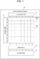
- Fig. 1 illustrates an example of an external appearance of an electric charge detection sensor 10 as viewed from above according to an embodiment of the present technology.
- the electric charge detection sensor 10 is a sensor that detects electric charge in solution.
- a detection area 11 is disposed on the upper surface of the electric charge detection sensor 10, and solution serving as a sample is soaked in the detection area 11.
- the electric charge detection sensor 10 includes a column selection unit 16, a row selection unit 17, an amplification unit 18, and an A/D conversion unit 19.
- the detection area 11 has a plurality of cells 12 each including a detection element, and the plurality of cells 12 is arranged in a two-dimensional array to form an element array. Each of the plurality of cells 12 detects electric charge. Note that this example shows an 8x8 element array, but this is only an example and an element array can have any size as necessary.
- the column selection unit 16 outputs a column selection signal for selecting a column of cells 12 in the two-dimensional array in the detection area 11.
- the row selection unit 17 outputs a row selection signal for selecting a row of cells 12 in the two-dimensional array in the detection area 11.
- the column selection unit 16 and the row selection unit 17 select identify one of the cells 12 in the two-dimensional array.
- the amplification unit 18 amplifies a potential signal from the cell 12 selected by the column selection unit 16 and the row selection unit 17.
- the A/D conversion unit 19 converts the potential signal amplified by the amplification unit 18 from an analog value to a digital value.
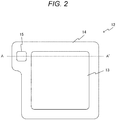
- Fig. 2 illustrates an example of an external appearance of a cell 12 as viewed from above according to the embodiment of the present technology.
- the cell 12 includes a detection unit 13 that detects electric charge, and is surrounded by an insulating portion 14 that insulates the cell 12 from other cells 12.
- the solution soaked in the detection area 11 is in contact with the detection unit 13. This allows each of the plurality of cells 12 to detect electric charge of ions in the solution that is in contact with the detection unit 13.
- each cell 12 may have a recess 15 in a part of the insulating portion 14. This is just an example for connecting the detection unit 13 to a wiring under the detection unit 13 as described later, and various other techniques can be conceived to achieve the connection.
- Fig. 3 illustrates an example of a sectional view of the electric charge detection sensor 10 as viewed from above according to the first embodiment of the present technology.
- a cross-section taken along line A-A' in Fig. 2 is illustrated.
- the electric charge detection sensor 10 includes a detection electrode 130 as the detection unit 13.
- the detection electrode 130 is a water-insoluble electrode using metal such as platinum (Pt) as a material, and a group of conductive nanoparticles each having a size on the order of nanometers is deposited on a surface of the detection electrode 130. It may be assumed that such a group of nanoparticles includes, for example, platinum nanoparticles.
- the electric charge detection sensor 10 includes an insulation layer 140 as the insulating portion 14.
- the insulation layer 140 insulates detection electrodes 130 arranged in an array from each other.
- As a material of the insulation layer 140 for example, silicon nitride (SiN) or the like can be used. Note that the insulation layer 140 is an example of an insulating portion described in the claims.
- An insulation layer 150 is disposed as a layer under the detection electrode 130.
- a material of the insulation layer 150 for example, silicon monoxide (SiO), silicon nitride (SiN), or the like can be used.
- a wiring layer 160 is disposed as a layer under the insulation layer 150.
- a material of the wiring layer 160 for example, titanium nitride (TiN), aluminum copper alloy (AlCu), or the like can be used.
- the detection electrode 130 is recessed downward along the recess 15 of the insulation layer 150, where the detection electrode 130 is connected with the wiring layer 160.
- the recess 15 may be filled with another material or the same material.
- An electrode 170 for connection with another layer is disposed under the wiring layer 160.
- a material of the electrode 170 for example, copper (Cu), or the like can be used. This allows for connection (Cu-Cu connection) between copper electrodes in different layers.
- Fig. 4 illustrates an example of a sectional view of the detection electrode 130 according to the embodiment of the present technology.
- the detection electrode 130 includes an electrode 131 that uses metal as a material, with a group of conductive nanoparticles 132 deposited on a surface of the electrode 131.
- the group of nanoparticles 132 is three-dimensionally deposited as illustrated. This allows for, as compared to a case where only the planar electrode 131 is included, an increase in surface area and a reduction in resistance of the detection electrode 130.
- the group of nanoparticles 132 is deposited by skin coating, that is, spraying the electrode 131 with nanoparticles.
- the deposition may also be performed by using a technique such as vapor-deposited film forming or sputtering.
- the group of nanoparticles 132 is an example of a group of particles described in the claims.
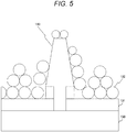
- Fig. 5 illustrates a first example of the shape of the insulation layer 140 according to the first embodiment of the present technology.
- the insulation layer 140 has a trapezoidal shape.
- the insulation layer 140 has side walls that spread downward, and has a planar top.
- Fig. 6 illustrates a second example of the shape of the insulation layer 140 according to the first embodiment of the present technology.
- the insulation layer 140 has a triangular shape.
- the insulation layer 140 has side walls that spread downward, and has a sharp top.
- Fig. 7 illustrates a third example of the shape of the insulation layer 140 according to the first embodiment of the present technology.
- the insulation layer 140 has a reverse taper shape.
- the insulation layer 140 has side walls that spread upward, and has a planar top.
- the group of nanoparticles 132 is three-dimensionally deposited on the surface of the detection electrode 130 in the electric charge detection sensor. This increases the surface area and reduces the resistance, thereby improving the sensing sensitivity.
- Fig. 8 illustrates an example of a sectional view of an electric charge detection sensor 10 according to a modified example of the first embodiment of the present technology.
- a plug-type contact 180 in which an insulating film and a conductor such as metal are embedded in a through hole penetrating the insulation layer 150 is disposed to connect the detection electrode 130 with the wiring layer 160.
- a material of the metal is, for example, tungsten (W) or the like.
- the contact 180 may be a through-silicon via (TSV)-type contact in which a conductor such as metal is attached to the bottom and side walls of the hole.
- TSV through-silicon via
- the detection electrode 130 can be formed into a planar shape, unlike the above-described first embodiment. Furthermore, the contact 180 can be disposed under the detection electrode 130, and this allows for an increase in area of the detection unit 13 (the area where the detection electrode 130 is exposed) and a further improvement in sensing sensitivity.
- the group of nanoparticles 132 is three-dimensionally deposited on the surface of the detection electrode 130 to increase the surface area.
- a conductive film is formed on the side walls of the insulation layer 140, and electric conduction is generated between adjacent detection electrodes 130 and may hinder normal operation.
- insulation is provided to prevent continuous covering formed by deposition. Note that an overall configuration of an electric charge detection sensor 10 is similar to that of the above-described first embodiment, and thus detailed description thereof is omitted.
- Fig. 9 illustrates an example of a sectional view of the electric charge detection sensor 10 according to the second embodiment of the present technology. Here, a cross-section taken along line A-A' in Fig. 2 is illustrated.
- an insulation layer 140 has eaves-shaped side walls. That is, the insulation layer 140 has a protruding shape at a portion away from the surface of a detection electrode 130 by a predetermined distance. This prevents continuous formation of a conductive film between detection electrodes 130.
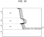
- Fig. 10 illustrates an example of a cross-sectional shape of a side wall portion of the insulation layer 140 according to the second embodiment of the present technology.
- the insulation layer 140 includes three layers: a first layer 141, a second layer 142, and a third layer 143.
- the first layer 141 uses silicon nitride (SiN) as a material.
- the second layer 142 is a layer that forms a protruding shape, and uses silicon monoxide (SiO) as a material.
- the third layer 143 uses silicon nitride (SiN) as a material.
- the reason for using different materials like this is to facilitate formation of an eaves shape on the side walls of the insulation layer 140.
- the eaves shape can be formed by using the same type of material.
- the materials exemplified here are examples, and other materials may be used to form the eaves shape.
- the protruding shape of the insulation layer 140 is disposed at a position higher than the height of a group of nanoparticles 132. That is, the third layer 143 is formed to have a thickness greater than the thickness of the group of nanoparticles 132.
- Each particle in the group of nanoparticles 132 has a size on the order of nanometers, and the thickness of the group of nanoparticles 132 formed by three-dimensionally depositing those particles is, for example, on the order of several tens of nanometers.
- the thickness of the third layer 143 under the second layer 142 forming the protruding shape is greater than the order of several tens of nanometers.
- the thickness of the third layer 143 is preferably about three times the thickness of the group of nanoparticles 132, for example.
- the horizontal length of protrusion of the protruding shape of the insulation layer 140 is arranged to be greater than the height of the group of nanoparticles 132. That is, the second layer 142 is formed so as to protrude beyond the third layer 143 by a length greater than the thickness of the group of nanoparticles 132.
- Forming the protruding shape having an appropriate height and length in the insulation layer 140 like this can prevent electric conduction between adjacent detection electrodes 130 caused by continuous covering formed by deposition of the group of nanoparticles 132.
- Fig. 11 illustrates an example of a shape of the insulation layer 140 according to the second embodiment of the present technology.
- the insulation layer 140 has a trapezoidal shape and has eaves-shaped side walls. That is, since the insulation layer 140 has eaves-shaped side walls, nanoparticles sprayed for deposition of the group of nanoparticles 132 are prevented from continuously covering over insulation layers 140.
- the insulation layer 140 having the eaves-shaped side walls prevents the deposited group of nanoparticles 132 from continuously covering over the insulation layers 140.
- Fig. 12 illustrates an example of a sectional view of the electric charge detection sensor 10 according to a modified example of the second embodiment of the present technology.
- a plug-type contact 180 in which an insulating film and a conductor such as metal are embedded in a through hole penetrating an insulation layer 150 is disposed to connect the detection electrode 130 with a wiring layer 160.
- a material of the metal is, for example, tungsten (W).
- the contact 180 may be a through-silicon via (TSV)-type contact in which a conductor such as metal is attached to the bottom and side walls of the hole.
- TSV through-silicon via
- This modified example of the second embodiment has effects similar to those of the above-described modified example of the first embodiment, thereby further improving the sensing sensitivity.
- an electric charge detection sensor 10 can detect electric charge in solution.
- an example of a case in which the electric charge detection sensor 10 is applied to a potential measurement system will be described.
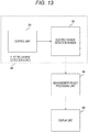
- Fig. 13 illustrates a configuration example of the potential measurement system according to the third embodiment of the present technology.
- This potential measurement system includes, in addition to the electric charge detection sensor 10 described in the above-described embodiments, a control unit 20, a measurement result processing unit 40, and a display unit 50.
- each of a plurality of cells 12 detects electric charge as described above. This allows for measurement of ions in the solution. This also allows for measurement of a biological activity or identification of a biological substance, thereby allowing the electric charge detection sensor 10 to function as a biosensor.
- the control unit 20 drives or controls the electric charge detection sensor 10. For example, the control unit 20 instructs the electric charge detection sensor 10 to start and end potential measurement, or controls choosing of a measurement target or the like.
- the measurement result processing unit 40 processes a result of measurement by the electric charge detection sensor 10 on the basis of a preset standard. For example, the measurement result processing unit 40 performs processing such as conversion of measurement data or multiple-level categorization of a numerical value in the measurement data in order to display the measurement result.
- the display unit 50 displays the measurement result processed by the measurement result processing unit 40.
- the display unit 50 shows the measurement result as colors and shades of pixels, two-dimensionally arranges the pixels in a similar manner to an element array, and displays the pixels as an image showing a distribution of electric charges or potentials.
- images obtained in such a manner can be chronologically displayed to display the images as a moving image showing a change in electric charge or potential.
- the electric charge detection sensor 10 and the control unit 20 constitute an electric charge detection device 30.
- the electric charge detection device 30 may be installed at a measurement target and store measurement results, and then the stored measurement results may be processed by the measurement result processing unit 40.
- the electric charge detection device 30 may have a network function so that results of measurement by the electric charge detection sensor 10 may be remotely transmitted in real time and processed by the measurement result processing unit 40 located away from the electric charge detection device 30.
- the electric charge detection sensor 10 described in the above-described embodiments can be used to perform measurement and display measurement results on the display unit 50.
- processing procedures described in the above-described embodiments may be regarded as a method including a series of these procedures, or may be regarded as a program for causing a computer to execute the series of these procedures or a recording medium that stores the program.
- a recording medium for example, a compact disc (CD), a MiniDisc (MD), a digital versatile disc (DVD), a memory card, a Blu-ray (registered trademark) disc, or the like can be used.
Landscapes
- Chemical & Material Sciences (AREA)
- Health & Medical Sciences (AREA)
- Life Sciences & Earth Sciences (AREA)
- General Physics & Mathematics (AREA)
- Physics & Mathematics (AREA)
- Chemical Kinetics & Catalysis (AREA)
- Molecular Biology (AREA)
- Electrochemistry (AREA)
- Analytical Chemistry (AREA)
- Biochemistry (AREA)
- General Health & Medical Sciences (AREA)
- Immunology (AREA)
- Pathology (AREA)
- Investigating Or Analyzing Materials By The Use Of Electric Means (AREA)
Abstract
Description
- The present technology relates to an electric charge detection sensor. Specifically, the present technology relates to an electric charge detection sensor and a potential measurement system using the electric charge detection sensor.
- Electric charge detection sensors that have a plurality of electrodes arranged in an array and detect electric charge generated in solution on each electrode have conventionally attracted attention. For example, a potential measuring device that measures a potential at an action potential generation point generated due to a chemical change has been proposed (see, for example, Patent Document 1).
- Patent Document 1:
WO 2017/061171 A - In the above-described conventional technology, electrodes arranged in an array are soaked in solution, and electric charge generated in the solution is detected. In order to improve a sensing sensitivity in the above-described electric charge detection sensors, it is conceivable to increase the area for sensing. However, increasing the areas of the electrodes themselves causes the area of the entire device to increase and makes downsizing difficult.
- The present technology has been developed in view of such a situation, and is aimed at improving a sensing sensitivity in an electric charge detection sensor.
- The present technology has been made to solve the above-described problems. A first aspect of the present technology is an electric charge detection sensor including a plurality of detection electrodes that is arranged in an array and detects electric charge, an insulating portion that insulates the plurality of detection electrodes from each other, and a group of conductive particles deposited on surfaces of the plurality of detection electrodes. This brings about an effect of increasing the surface area of each detection electrode and reducing a resistance, thereby improving the sensing sensitivity.
- Furthermore, in the first aspect, the group of particles may be a group of nanoparticles each having a size on the order of nanometers. More specifically, the group of particles may be a group of platinum nanoparticles. This brings about an effect of three-dimensionally depositing a group of nanoparticles on the surface of each detection electrode, thereby increasing the surface area.
- Furthermore, in the first aspect, the plurality of detection electrodes may be water-insoluble electrodes using metal as a material. More specifically, the plurality of detection electrodes may be electrodes using platinum as a material. This brings about an effect of encasing the electric charge detection sensor with a metal material when the group of nanoparticles is deposited.
- Furthermore, in the first aspect, the insulating portion may have a protruding shape at a portion away from the surface of each detection electrode by a predetermined distance. This brings about an effect of preventing a conductive film from being formed on side walls of an insulation layer.
- Furthermore, in the first aspect, the protruding shape of the insulating portion is preferably disposed at a position higher than the height of the group of particles. Furthermore, the protruding shape of the insulating portion preferably has a protrusion longer than the height of the group of particles. This ensures the effect of preventing a conductive film from being formed on the side walls of the insulation layer.
- Furthermore, in the first aspect, the protruding shape of the insulating portion may be formed by using a material different from the material of other portions of the insulating portion. This brings about an effect of facilitating formation of a protruding shape on an insulation layer.
- Furthermore, in the first aspect, each of the plurality of detection electrodes may include a recess for connection with a wiring layer. This brings about an effect of allowing each detection electrode to be connected to a wiring layer.
- Furthermore, in the first aspect, a contact may be further included to allow each of the plurality of detection electrodes to be connected to the wiring layer. The contact may be a metal-embedded plug-type contact or a through silicon via type contact. This brings about an effect of allowing each detection electrode to be connected to the wiring layer by using the contact.
- Furthermore, in the first aspect, the electric charge detection sensor may detect ions in solution that is in contact with each detection electrode.
- Furthermore, in the first aspect, the electric charge detection sensor may be a biosensor that detects the electric charge to measure a biological activity or identify a biological substance.
- Furthermore, a second aspect of the present technology may be a potential measurement system including: an electric charge detection sensor that includes a plurality of detection electrodes that is arranged in an array and detects electric charge, an insulating portion that insulates the plurality of detection electrodes from each other, and a group of conductive particles deposited on surfaces of the plurality of detection electrodes, and performs potential measurement; a control unit that controls potential measurement in the electric charge detection sensor; a measurement result processing unit that processes a result of measurement by the electric charge detection sensor; and a display unit that displays the processed measurement result. This brings about an effect of processing the result of measurement by the electric charge detection sensor and displaying the result as an image or a moving image.
- The present technology can produce an excellent effect of improving the sensing sensitivity in the electric charge detection sensor. Note that the effects described here are not necessarily restrictive, and the effects of the invention may be any of the effects described in the present disclosure.
-
-
Fig. 1 illustrates an example of an external appearance of an electriccharge detection sensor 10 as viewed from above according to an embodiment of the present technology. -
Fig. 2 illustrates an example of an external appearance of acell 12 as viewed from above according to the embodiment of the present technology. -
Fig. 3 illustrates an example of a sectional view of the electriccharge detection sensor 10 as viewed from above according to the first embodiment of the present technology. -
Fig. 4 illustrates an example of a sectional view of adetection electrode 130 according to the embodiment of the present technology. -
Fig. 5 illustrates a first example of a shape of aninsulation layer 140 according to the first embodiment of the present technology. -
Fig. 6 illustrates a second example of a shape of theinsulation layer 140 according to the first embodiment of the present technology. -
Fig. 7 illustrates a third example of a shape of theinsulation layer 140 according to the first embodiment of the present technology. -
Fig. 8 illustrates an example of a sectional view of an electriccharge detection sensor 10 according to a modified example of the first embodiment of the present technology. -
Fig. 9 illustrates an example of a sectional view of an electriccharge detection sensor 10 according to a second embodiment of the present technology. -
Fig. 10 illustrates an example of a cross-sectional shape of a side wall portion of aninsulation layer 140 according to the second embodiment of the present technology. -
Fig. 11 illustrates an example of a shape of theinsulation layer 140 according to the second embodiment of the present technology. -
Fig. 12 illustrates an example of a sectional view of the electriccharge detection sensor 10 according to a modified example of the second embodiment of the present technology. -
Fig. 13 illustrates a configuration example of a potential measurement system according to a third embodiment of the present technology. - Modes for carrying out the present technology (hereinafter referred to as "embodiments") will be described below. The description will be made in the following order.
- 1. First embodiment (example in which platinum nanoparticles are used to form a three-dimensional electrode)
- 2. Second embodiment (example in which side walls of an insulating portion between electrodes have an eaves shape)
- 3. Third embodiment (example of application to a potential measurement system)
-
Fig. 1 illustrates an example of an external appearance of an electriccharge detection sensor 10 as viewed from above according to an embodiment of the present technology. - The electric
charge detection sensor 10 is a sensor that detects electric charge in solution. Adetection area 11 is disposed on the upper surface of the electriccharge detection sensor 10, and solution serving as a sample is soaked in thedetection area 11. Furthermore, the electriccharge detection sensor 10 includes acolumn selection unit 16, arow selection unit 17, anamplification unit 18, and an A/D conversion unit 19. - The
detection area 11 has a plurality ofcells 12 each including a detection element, and the plurality ofcells 12 is arranged in a two-dimensional array to form an element array. Each of the plurality ofcells 12 detects electric charge. Note that this example shows an 8x8 element array, but this is only an example and an element array can have any size as necessary. - The
column selection unit 16 outputs a column selection signal for selecting a column ofcells 12 in the two-dimensional array in thedetection area 11. Therow selection unit 17 outputs a row selection signal for selecting a row ofcells 12 in the two-dimensional array in thedetection area 11. Thecolumn selection unit 16 and therow selection unit 17 select identify one of thecells 12 in the two-dimensional array. - The
amplification unit 18 amplifies a potential signal from thecell 12 selected by thecolumn selection unit 16 and therow selection unit 17. - The A/
D conversion unit 19 converts the potential signal amplified by theamplification unit 18 from an analog value to a digital value. -
Fig. 2 illustrates an example of an external appearance of acell 12 as viewed from above according to the embodiment of the present technology. - The
cell 12 includes adetection unit 13 that detects electric charge, and is surrounded by an insulatingportion 14 that insulates thecell 12 fromother cells 12. The solution soaked in thedetection area 11 is in contact with thedetection unit 13. This allows each of the plurality ofcells 12 to detect electric charge of ions in the solution that is in contact with thedetection unit 13. - Note that each
cell 12 may have arecess 15 in a part of the insulatingportion 14. This is just an example for connecting thedetection unit 13 to a wiring under thedetection unit 13 as described later, and various other techniques can be conceived to achieve the connection. -
Fig. 3 illustrates an example of a sectional view of the electriccharge detection sensor 10 as viewed from above according to the first embodiment of the present technology. Here, a cross-section taken along line A-A' inFig. 2 is illustrated. - The electric
charge detection sensor 10 includes adetection electrode 130 as thedetection unit 13. Thedetection electrode 130 is a water-insoluble electrode using metal such as platinum (Pt) as a material, and a group of conductive nanoparticles each having a size on the order of nanometers is deposited on a surface of thedetection electrode 130. It may be assumed that such a group of nanoparticles includes, for example, platinum nanoparticles. - The electric
charge detection sensor 10 includes aninsulation layer 140 as the insulatingportion 14. Theinsulation layer 140 insulatesdetection electrodes 130 arranged in an array from each other. As a material of theinsulation layer 140, for example, silicon nitride (SiN) or the like can be used. Note that theinsulation layer 140 is an example of an insulating portion described in the claims. - An
insulation layer 150 is disposed as a layer under thedetection electrode 130. As a material of theinsulation layer 150, for example, silicon monoxide (SiO), silicon nitride (SiN), or the like can be used. - A
wiring layer 160 is disposed as a layer under theinsulation layer 150. As a material of thewiring layer 160, for example, titanium nitride (TiN), aluminum copper alloy (AlCu), or the like can be used. - As illustrated, the
detection electrode 130 is recessed downward along therecess 15 of theinsulation layer 150, where thedetection electrode 130 is connected with thewiring layer 160. Note that therecess 15 may be filled with another material or the same material. - An
electrode 170 for connection with another layer is disposed under thewiring layer 160. As a material of theelectrode 170, for example, copper (Cu), or the like can be used. This allows for connection (Cu-Cu connection) between copper electrodes in different layers. -
Fig. 4 illustrates an example of a sectional view of thedetection electrode 130 according to the embodiment of the present technology. - As described above, the
detection electrode 130 includes anelectrode 131 that uses metal as a material, with a group ofconductive nanoparticles 132 deposited on a surface of theelectrode 131. The group ofnanoparticles 132 is three-dimensionally deposited as illustrated. This allows for, as compared to a case where only theplanar electrode 131 is included, an increase in surface area and a reduction in resistance of thedetection electrode 130. - It may be assumed that the group of
nanoparticles 132 is deposited by skin coating, that is, spraying theelectrode 131 with nanoparticles. The deposition may also be performed by using a technique such as vapor-deposited film forming or sputtering. Note that the group ofnanoparticles 132 is an example of a group of particles described in the claims. - The embodiment has been described above on the assumption that the
insulation layer 140 in the insulatingportion 14 has vertical side walls. Alternatively, various shapes can be applied as a shape of theinsulation layer 140 as exemplified below. -
Fig. 5 illustrates a first example of the shape of theinsulation layer 140 according to the first embodiment of the present technology. In the first example, theinsulation layer 140 has a trapezoidal shape. Theinsulation layer 140 has side walls that spread downward, and has a planar top. -
Fig. 6 illustrates a second example of the shape of theinsulation layer 140 according to the first embodiment of the present technology. In the second example, theinsulation layer 140 has a triangular shape. Theinsulation layer 140 has side walls that spread downward, and has a sharp top. -
Fig. 7 illustrates a third example of the shape of theinsulation layer 140 according to the first embodiment of the present technology. In the third example, theinsulation layer 140 has a reverse taper shape. Theinsulation layer 140 has side walls that spread upward, and has a planar top. - In this way, according to the first embodiment of the present technology, the group of
nanoparticles 132 is three-dimensionally deposited on the surface of thedetection electrode 130 in the electric charge detection sensor. This increases the surface area and reduces the resistance, thereby improving the sensing sensitivity. -
Fig. 8 illustrates an example of a sectional view of an electriccharge detection sensor 10 according to a modified example of the first embodiment of the present technology. - In this modified example, a plug-
type contact 180 in which an insulating film and a conductor such as metal are embedded in a through hole penetrating theinsulation layer 150 is disposed to connect thedetection electrode 130 with thewiring layer 160. In this case, it may be assumed that a material of the metal is, for example, tungsten (W) or the like. - Note that the
contact 180 may be a through-silicon via (TSV)-type contact in which a conductor such as metal is attached to the bottom and side walls of the hole. - According to this modified example, the
detection electrode 130 can be formed into a planar shape, unlike the above-described first embodiment. Furthermore, thecontact 180 can be disposed under thedetection electrode 130, and this allows for an increase in area of the detection unit 13 (the area where thedetection electrode 130 is exposed) and a further improvement in sensing sensitivity. - In the above-described first embodiment, the group of
nanoparticles 132 is three-dimensionally deposited on the surface of thedetection electrode 130 to increase the surface area. In this case, a conductive film is formed on the side walls of theinsulation layer 140, and electric conduction is generated betweenadjacent detection electrodes 130 and may hinder normal operation. For this reason, in this second embodiment, insulation is provided to prevent continuous covering formed by deposition. Note that an overall configuration of an electriccharge detection sensor 10 is similar to that of the above-described first embodiment, and thus detailed description thereof is omitted. -
Fig. 9 illustrates an example of a sectional view of the electriccharge detection sensor 10 according to the second embodiment of the present technology. Here, a cross-section taken along line A-A' inFig. 2 is illustrated. - In the second embodiment, an
insulation layer 140 has eaves-shaped side walls. That is, theinsulation layer 140 has a protruding shape at a portion away from the surface of adetection electrode 130 by a predetermined distance. This prevents continuous formation of a conductive film betweendetection electrodes 130. -
Fig. 10 illustrates an example of a cross-sectional shape of a side wall portion of theinsulation layer 140 according to the second embodiment of the present technology. - In this example, the
insulation layer 140 includes three layers: afirst layer 141, asecond layer 142, and athird layer 143. Thefirst layer 141 uses silicon nitride (SiN) as a material. Thesecond layer 142 is a layer that forms a protruding shape, and uses silicon monoxide (SiO) as a material. Thethird layer 143 uses silicon nitride (SiN) as a material. The reason for using different materials like this is to facilitate formation of an eaves shape on the side walls of theinsulation layer 140. Note that, the eaves shape can be formed by using the same type of material. Furthermore, the materials exemplified here are examples, and other materials may be used to form the eaves shape. - The protruding shape of the
insulation layer 140 is disposed at a position higher than the height of a group ofnanoparticles 132. That is, thethird layer 143 is formed to have a thickness greater than the thickness of the group ofnanoparticles 132. Each particle in the group ofnanoparticles 132 has a size on the order of nanometers, and the thickness of the group ofnanoparticles 132 formed by three-dimensionally depositing those particles is, for example, on the order of several tens of nanometers. Thus, the thickness of thethird layer 143 under thesecond layer 142 forming the protruding shape is greater than the order of several tens of nanometers. Considering piling up of particles in the group ofnanoparticles 132, the thickness of thethird layer 143 is preferably about three times the thickness of the group ofnanoparticles 132, for example. - Furthermore, the horizontal length of protrusion of the protruding shape of the
insulation layer 140 is arranged to be greater than the height of the group ofnanoparticles 132. That is, thesecond layer 142 is formed so as to protrude beyond thethird layer 143 by a length greater than the thickness of the group ofnanoparticles 132. - Forming the protruding shape having an appropriate height and length in the
insulation layer 140 like this can prevent electric conduction betweenadjacent detection electrodes 130 caused by continuous covering formed by deposition of the group ofnanoparticles 132. -
Fig. 11 illustrates an example of a shape of theinsulation layer 140 according to the second embodiment of the present technology. - In this example, the
insulation layer 140 has a trapezoidal shape and has eaves-shaped side walls. That is, since theinsulation layer 140 has eaves-shaped side walls, nanoparticles sprayed for deposition of the group ofnanoparticles 132 are prevented from continuously covering over insulation layers 140. - In this way, according to the second embodiment of the present technology, the
insulation layer 140 having the eaves-shaped side walls prevents the deposited group ofnanoparticles 132 from continuously covering over the insulation layers 140. -
Fig. 12 illustrates an example of a sectional view of the electriccharge detection sensor 10 according to a modified example of the second embodiment of the present technology. - In this modified example, as in the above-described first embodiment, a plug-
type contact 180 in which an insulating film and a conductor such as metal are embedded in a through hole penetrating aninsulation layer 150 is disposed to connect thedetection electrode 130 with awiring layer 160. In this case, it may be assumed that a material of the metal is, for example, tungsten (W). Furthermore, thecontact 180 may be a through-silicon via (TSV)-type contact in which a conductor such as metal is attached to the bottom and side walls of the hole. - This modified example of the second embodiment has effects similar to those of the above-described modified example of the first embodiment, thereby further improving the sensing sensitivity.
- As described in the above-described embodiments, an electric
charge detection sensor 10 can detect electric charge in solution. In this third embodiment, an example of a case in which the electriccharge detection sensor 10 is applied to a potential measurement system will be described. -
Fig. 13 illustrates a configuration example of the potential measurement system according to the third embodiment of the present technology. This potential measurement system includes, in addition to the electriccharge detection sensor 10 described in the above-described embodiments, acontrol unit 20, a measurementresult processing unit 40, and adisplay unit 50. - In the electric
charge detection sensor 10, each of a plurality ofcells 12 detects electric charge as described above. This allows for measurement of ions in the solution. This also allows for measurement of a biological activity or identification of a biological substance, thereby allowing the electriccharge detection sensor 10 to function as a biosensor. - The
control unit 20 drives or controls the electriccharge detection sensor 10. For example, thecontrol unit 20 instructs the electriccharge detection sensor 10 to start and end potential measurement, or controls choosing of a measurement target or the like. - The measurement
result processing unit 40 processes a result of measurement by the electriccharge detection sensor 10 on the basis of a preset standard. For example, the measurementresult processing unit 40 performs processing such as conversion of measurement data or multiple-level categorization of a numerical value in the measurement data in order to display the measurement result. - The
display unit 50 displays the measurement result processed by the measurementresult processing unit 40. For example, thedisplay unit 50 shows the measurement result as colors and shades of pixels, two-dimensionally arranges the pixels in a similar manner to an element array, and displays the pixels as an image showing a distribution of electric charges or potentials. Furthermore, for example, images obtained in such a manner can be chronologically displayed to display the images as a moving image showing a change in electric charge or potential. - In this example, the electric
charge detection sensor 10 and thecontrol unit 20 constitute an electriccharge detection device 30. For example, the electriccharge detection device 30 may be installed at a measurement target and store measurement results, and then the stored measurement results may be processed by the measurementresult processing unit 40. Furthermore, the electriccharge detection device 30 may have a network function so that results of measurement by the electriccharge detection sensor 10 may be remotely transmitted in real time and processed by the measurementresult processing unit 40 located away from the electriccharge detection device 30. - In this way, according to the third embodiment of the present technology, the electric
charge detection sensor 10 described in the above-described embodiments can be used to perform measurement and display measurement results on thedisplay unit 50. - Note that the above-described embodiments show examples for embodying the present technology, and the matters in the embodiments correspond to the matters specifying the invention in the claims. Similarly, the matters specifying the invention in the claims correspond to the matters in the embodiments of the present technology having the same names. However, the present technology is not limited to the embodiments, and can be embodied by making a wide variety of modifications to the embodiments without departing from the gist thereof.
- Furthermore, the processing procedures described in the above-described embodiments may be regarded as a method including a series of these procedures, or may be regarded as a program for causing a computer to execute the series of these procedures or a recording medium that stores the program. As the recording medium, for example, a compact disc (CD), a MiniDisc (MD), a digital versatile disc (DVD), a memory card, a Blu-ray (registered trademark) disc, or the like can be used.
- Note that effects described herein are merely illustrative and are not intended to be restrictive, and other effects may be obtained.
- Note that the present technology can also be configured as described below.
- (1) An electric charge detection sensor including:
- a plurality of detection electrodes that is arranged in an array and detects electric charge;
- an insulating portion that insulates the plurality of detection electrodes from each other; and
- a group of conductive particles deposited on surfaces of the plurality of detection electrodes.
- (2) The electric charge detection sensor according to (1), in which
the group of particles is a group of nanoparticles each having a size on the order of nanometers. - (3) The electric charge detection sensor according to (2), in which
the group of particles is a group of platinum nanoparticles. - (4) The electric charge detection sensor according to any one of (1) to (3), in which
the plurality of detection electrodes is water-insoluble electrodes using metal as a material. - (5) The electric charge detection sensor according to (4), in which
the plurality of detection electrodes is electrodes using platinum as a material. - (6) The electric charge detection sensor according to any one of (1) to (5), in which
the insulating portion has a protruding shape at a portion away from a surface of each detection electrode by a predetermined distance. - (7) The electric charge detection sensor according to (6), in which
the protruding shape of the insulating portion is disposed at a position higher than the height of the group of particles. - (8) The electric charge detection sensor according to (6) or (7), in which
the protruding shape of the insulating portion has a protrusion longer than the height of the group of particles. - (9) The electric charge detection sensor according to any one of (6) to (8), in which
the protruding shape of the insulating portion is formed by using a material different from a material of other portions of the insulating portion. - (10) The electric charge detection sensor according to any one of (1) to (9), in which
each of the plurality of detection electrodes has a recess for connection with a wiring layer. - (11) The electric charge detection sensor according to any one of (1) to (10), further including a contact for connecting each of the plurality of detection electrodes to a wiring layer.
- (12) The electric charge detection sensor according to (11), in which
the contact is a metal-embedded plug-type contact. - (13) The electric charge detection sensor according to (11), in which
the contact is a through silicon via type contact. - (14) The electric charge detection sensor according to any one of (1) to (13), in which the electric charge detection sensor detects ions in solution that is in contact with each detection electrode.
- (15) The electric charge detection sensor according to any one of (1) to (14), in which the electric charge detection sensor includes a biosensor that detects the electric charge to measure a biological activity or identify a biological substance.
- (16) A potential measurement system including:
- an electric charge detection sensor that includes a plurality of detection electrodes that is arranged in an array and detects electric charge, an insulating portion that insulates the plurality of detection electrodes from each other, and a group of conductive particles deposited on surfaces of the plurality of detection electrodes, and performs potential measurement;
- a control unit that controls potential measurement in the electric charge detection sensor;
- a measurement result processing unit that processes a result of measurement by the electric charge detection sensor; and
- a display unit that displays the processed measurement result.
-
- 10
- Electric charge detection sensor
- 11
- Detection area
- 12
- Cell
- 13
- Detection unit
- 14
- Insulating portion
- 15
- Recess
- 16
- Column selection unit
- 17
- Row selection unit
- 18
- Amplification unit
- 19
- A/D conversion unit
- 20
- Control unit
- 30
- Electric charge detection device
- 40
- Measurement result processing unit
- 50
- Display unit
- 130
- Detection electrode
- 131
- Electrode
- 132
- Group of nanoparticles
- 140 to 143, 150
- Insulation layer
- 160
- Wiring layer
- 170
- Electrode
- 180
- Contact
Claims (16)
- An electric charge detection sensor comprising:a plurality of detection electrodes that is arranged in an array and detects electric charge;an insulating portion that insulates the plurality of detection electrodes from each other; anda group of conductive particles deposited on surfaces of the plurality of detection electrodes.
- The electric charge detection sensor according to claim 1, wherein
the group of particles is a group of nanoparticles each having a size on order of nanometers. - The electric charge detection sensor according to claim 2, wherein
the group of particles is a group of platinum nanoparticles. - The electric charge detection sensor according to claim 1, wherein
the plurality of detection electrodes is water-insoluble electrodes using metal as a material. - The electric charge detection sensor according to claim 4, wherein
the plurality of detection electrodes is electrodes using platinum as a material. - The electric charge detection sensor according to claim 1, wherein
the insulating portion has a protruding shape at a portion away from a surface of each detection electrode by a predetermined distance. - The electric charge detection sensor according to claim 6, wherein
the protruding shape of the insulating portion is disposed at a position higher than a height of the group of particles. - The electric charge detection sensor according to claim 6, wherein
the protruding shape of the insulating portion has a protrusion longer than a height of the group of particles. - The electric charge detection sensor according to claim 6, wherein
the protruding shape of the insulating portion is formed by using a material different from a material of other portions of the insulating portion. - The electric charge detection sensor according to claim 1, wherein
each of the plurality of detection electrodes has a recess for connection with a wiring layer. - The electric charge detection sensor according to claim 1, further comprising a contact for connecting each of the plurality of detection electrodes to a wiring layer.
- The electric charge detection sensor according to claim 11, wherein
the contact is a metal-embedded plug-type contact. - The electric charge detection sensor according to claim 11, wherein
the contact is a through silicon via type contact. - The electric charge detection sensor according to claim 1, wherein the electric charge detection sensor detects ions in solution that is in contact with each detection electrode.
- The electric charge detection sensor according to claim 1, wherein the electric charge detection sensor comprises a biosensor that detects the electric charge to measure a biological activity or identify a biological substance.
- A potential measurement system comprising:an electric charge detection sensor that includes a plurality of detection electrodes that is arranged in an array and detects electric charge, an insulating portion that insulates the plurality of detection electrodes from each other, and a group of conductive particles deposited on surfaces of the plurality of detection electrodes, and performs potential measurement;a control unit that controls potential measurement in the electric charge detection sensor;a measurement result processing unit that processes a result of measurement by the electric charge detection sensor; anda display unit that displays the processed measurement result.
Applications Claiming Priority (2)
| Application Number | Priority Date | Filing Date | Title |
|---|---|---|---|
| JP2017201458 | 2017-10-18 | ||
| PCT/JP2018/025666 WO2019077814A1 (en) | 2017-10-18 | 2018-07-06 | Charge detection sensor and potential measuring system |
Publications (2)
| Publication Number | Publication Date |
|---|---|
| EP3699613A4 EP3699613A4 (en) | 2020-08-26 |
| EP3699613A1 true EP3699613A1 (en) | 2020-08-26 |
Family
ID=66173210
Family Applications (1)
| Application Number | Title | Priority Date | Filing Date |
|---|---|---|---|
| EP18869061.4A Withdrawn EP3699613A1 (en) | 2017-10-18 | 2018-07-06 | Charge detection sensor and potential measuring system |
Country Status (5)
| Country | Link |
|---|---|
| US (1) | US20200319130A1 (en) |
| EP (1) | EP3699613A1 (en) |
| JP (1) | JPWO2019077814A1 (en) |
| CN (1) | CN111133323A (en) |
| WO (1) | WO2019077814A1 (en) |
Families Citing this family (2)
| Publication number | Priority date | Publication date | Assignee | Title |
|---|---|---|---|---|
| JP2019056581A (en) * | 2017-09-20 | 2019-04-11 | ソニーセミコンダクタソリューションズ株式会社 | Charge detection sensor and potential measurement system |
| CN116840323A (en) * | 2022-03-23 | 2023-10-03 | 群创光电股份有限公司 | Sensing electronic device |
Family Cites Families (23)
| Publication number | Priority date | Publication date | Assignee | Title |
|---|---|---|---|---|
| JPH01216250A (en) * | 1988-02-24 | 1989-08-30 | Matsushita Electric Works Ltd | Electrochemical sensor |
| JP3204875B2 (en) * | 1994-06-13 | 2001-09-04 | 松下電器産業株式会社 | Cell potential measurement device |
| KR960009188A (en) * | 1994-08-10 | 1996-03-22 | 김주용 | Method for manufacturing charge storage electrode of semiconductor device |
| US7287412B2 (en) * | 2003-06-03 | 2007-10-30 | Nano-Proprietary, Inc. | Method and apparatus for sensing hydrogen gas |
| JP2004239808A (en) * | 2003-02-07 | 2004-08-26 | Sony Corp | Surface potential sensor |
| JP2005077210A (en) * | 2003-08-29 | 2005-03-24 | National Institute For Materials Science | Biomolecule detection element and nucleic acid analysis method using the same |
| CN1590998A (en) * | 2003-09-06 | 2005-03-09 | 鸿富锦精密工业(深圳)有限公司 | Gas sensor |
| US20050244811A1 (en) * | 2003-12-15 | 2005-11-03 | Nano-Proprietary, Inc. | Matrix array nanobiosensor |
| US20070029195A1 (en) * | 2005-08-03 | 2007-02-08 | Changming Li | Polymer/nanoparticle composites, film and molecular detection device |
| JP5120874B2 (en) * | 2007-06-22 | 2013-01-16 | 株式会社船井電機新応用技術研究所 | Switching element |
| JP5121365B2 (en) * | 2007-09-21 | 2013-01-16 | 京セラ株式会社 | Solar cell module and manufacturing method thereof |
| US8715981B2 (en) * | 2009-01-27 | 2014-05-06 | Purdue Research Foundation | Electrochemical biosensor |
| GB2475063A (en) * | 2009-11-04 | 2011-05-11 | Univ Leicester | Charge detector for photons or particles. |
| JP5660533B2 (en) * | 2010-08-25 | 2015-01-28 | 国立大学法人名古屋大学 | Current detector |
| KR101305198B1 (en) * | 2011-12-09 | 2013-09-26 | 현대자동차주식회사 | Particulate matters sensor unit |
| KR20140012580A (en) * | 2012-07-19 | 2014-02-03 | 한국전자통신연구원 | An electrode sensor and method of fabrication the same |
| WO2014025044A1 (en) * | 2012-08-10 | 2014-02-13 | 国立大学法人豊橋技術科学大学 | Device for measuring oxidation-reduction potential and method for measuring oxidation-reduction potential |
| CN104685629B (en) * | 2012-09-28 | 2016-04-06 | 富士胶片株式会社 | Radiation detection element and radiation image detection device |
| US10067398B2 (en) * | 2013-03-22 | 2018-09-04 | Vlyte Innovations Limited | Electrophoretic device having a transparent light state |
| US10370694B2 (en) * | 2015-05-19 | 2019-08-06 | New York University | Size dependence of nanoparticle-protein interaction and high sensitivity potentiometric sensor exploiting such interactions |
| CN108140649B (en) * | 2015-10-01 | 2022-05-06 | 奥林巴斯株式会社 | Camera elements, endoscopes and endoscope systems |
| EP3361242B1 (en) | 2015-10-09 | 2022-04-27 | Sony Semiconductor Solutions Corporation | Potential measuring device |
| KR101903984B1 (en) * | 2015-11-25 | 2018-10-04 | 동우 화인켐 주식회사 | Connections for electrode and touch screen panel comprising the same |
-
2018
- 2018-07-06 WO PCT/JP2018/025666 patent/WO2019077814A1/en not_active Ceased
- 2018-07-06 US US16/755,220 patent/US20200319130A1/en not_active Abandoned
- 2018-07-06 CN CN201880061891.8A patent/CN111133323A/en active Pending
- 2018-07-06 JP JP2019549115A patent/JPWO2019077814A1/en active Pending
- 2018-07-06 EP EP18869061.4A patent/EP3699613A1/en not_active Withdrawn
Also Published As
| Publication number | Publication date |
|---|---|
| WO2019077814A1 (en) | 2019-04-25 |
| US20200319130A1 (en) | 2020-10-08 |
| CN111133323A (en) | 2020-05-08 |
| EP3699613A4 (en) | 2020-08-26 |
| JPWO2019077814A1 (en) | 2020-11-26 |
Similar Documents
| Publication | Publication Date | Title |
|---|---|---|
| US20200319130A1 (en) | Electric charge detection sensor and potential measurement system | |
| US9382575B2 (en) | Biomolecule detection apparatus including plurality of electrodes | |
| US9490204B2 (en) | Noise shielding techniques for ultra low current measurements in biochemical applications | |
| US6255678B1 (en) | Apparatus for measuring physical and chemical phenomena | |
| EP1712891A2 (en) | Molecular resonant tunneling sensor and methods of fabricating and using the same | |
| Muguet et al. | Combining PEDOT: PSS polymer coating with metallic 3D nanowires electrodes to achieve high electrochemical performances for neuronal interfacing applications | |
| Moreno-Hagelsieb et al. | Electrical detection of DNA hybridization: three extraction techniques based on interdigitated Al/Al2O3 capacitors | |
| Abe et al. | Redox cycling-based electrochemical CMOS imaging sensor for real time and selective imaging of redox analytes | |
| TWI534426B (en) | A method for biological detection | |
| WO2014088403A1 (en) | A resistive gas sensor device | |
| Liu et al. | Theory of electrochemistry for nanometer-sized disk electrodes | |
| CN205049507U (en) | Three -dimensional ECT and compound sensor device of ERT bimodal | |
| JPWO2019073774A1 (en) | Sensor device and measuring device | |
| Payne et al. | Identifying nanoscale pinhole defects in nitroaryl layers with scanning electrochemical cell microscopy | |
| US9097654B2 (en) | Electrode assembly | |
| US11906563B2 (en) | Electric potential measuring device and method for manufacturing electric potential measuring device | |
| US10433370B2 (en) | Micro multi-array heater and micro multi-array sensor | |
| JP3688611B2 (en) | Sensor array | |
| Krause et al. | Brownian motion in electrochemical nanodevices | |
| KR101631479B1 (en) | Electrode Array for analyzing electrical characteristics of Cell Spheroid | |
| JP2013057574A (en) | Soil sensor | |
| Aldhoon et al. | Unipolar voltage abnormality is associated with greater left ventricular dysfunction in ischemic cardiomyopathy | |
| Bratov et al. | Chemical sensors and biosensors based on impedimetric interdigitated electrode array transducers | |
| US20200271710A1 (en) | Charge detection sensor and potential measurement system | |
| JP5542807B2 (en) | Gas sensor |
Legal Events
| Date | Code | Title | Description |
|---|---|---|---|
| STAA | Information on the status of an ep patent application or granted ep patent |
Free format text: STATUS: THE INTERNATIONAL PUBLICATION HAS BEEN MADE |
|
| PUAI | Public reference made under article 153(3) epc to a published international application that has entered the european phase |
Free format text: ORIGINAL CODE: 0009012 |
|
| STAA | Information on the status of an ep patent application or granted ep patent |
Free format text: STATUS: REQUEST FOR EXAMINATION WAS MADE |
|
| 17P | Request for examination filed |
Effective date: 20200408 |
|
| A4 | Supplementary search report drawn up and despatched |
Effective date: 20200630 |
|
| AK | Designated contracting states |
Kind code of ref document: A1 Designated state(s): AL AT BE BG CH CY CZ DE DK EE ES FI FR GB GR HR HU IE IS IT LI LT LU LV MC MK MT NL NO PL PT RO RS SE SI SK SM TR |
|
| AX | Request for extension of the european patent |
Extension state: BA ME |
|
| DAV | Request for validation of the european patent (deleted) | ||
| DAX | Request for extension of the european patent (deleted) | ||
| STAA | Information on the status of an ep patent application or granted ep patent |
Free format text: STATUS: THE APPLICATION HAS BEEN WITHDRAWN |
|
| 18W | Application withdrawn |
Effective date: 20220905 |