EP3696608A1 - Measurement apparatus, exposure apparatus, and method of manufacturing article - Google Patents
Measurement apparatus, exposure apparatus, and method of manufacturing article Download PDFInfo
- Publication number
- EP3696608A1 EP3696608A1 EP20154931.8A EP20154931A EP3696608A1 EP 3696608 A1 EP3696608 A1 EP 3696608A1 EP 20154931 A EP20154931 A EP 20154931A EP 3696608 A1 EP3696608 A1 EP 3696608A1
- Authority
- EP
- European Patent Office
- Prior art keywords
- mark
- distance
- detector
- wafer
- processor
- Prior art date
- Legal status (The legal status is an assumption and is not a legal conclusion. Google has not performed a legal analysis and makes no representation as to the accuracy of the status listed.)
- Granted
Links
Images

Classifications
-
- G—PHYSICS
- G03—PHOTOGRAPHY; CINEMATOGRAPHY; ANALOGOUS TECHNIQUES USING WAVES OTHER THAN OPTICAL WAVES; ELECTROGRAPHY; HOLOGRAPHY
- G03F—PHOTOMECHANICAL PRODUCTION OF TEXTURED OR PATTERNED SURFACES, e.g. FOR PRINTING, FOR PROCESSING OF SEMICONDUCTOR DEVICES; MATERIALS THEREFOR; ORIGINALS THEREFOR; APPARATUS SPECIALLY ADAPTED THEREFOR
- G03F9/00—Registration or positioning of originals, masks, frames, photographic sheets or textured or patterned surfaces, e.g. automatically
- G03F9/70—Registration or positioning of originals, masks, frames, photographic sheets or textured or patterned surfaces, e.g. automatically for microlithography
- G03F9/7073—Alignment marks and their environment
- G03F9/7084—Position of mark on substrate, i.e. position in (x, y, z) of mark, e.g. buried or resist covered mark, mark on rearside, at the substrate edge, in the circuit area, latent image mark, marks in plural levels
-
- G—PHYSICS
- G01—MEASURING; TESTING
- G01B—MEASURING LENGTH, THICKNESS OR SIMILAR LINEAR DIMENSIONS; MEASURING ANGLES; MEASURING AREAS; MEASURING IRREGULARITIES OF SURFACES OR CONTOURS
- G01B11/00—Measuring arrangements characterised by the use of optical techniques
- G01B11/002—Measuring arrangements characterised by the use of optical techniques for measuring two or more coordinates
-
- G—PHYSICS
- G01—MEASURING; TESTING
- G01B—MEASURING LENGTH, THICKNESS OR SIMILAR LINEAR DIMENSIONS; MEASURING ANGLES; MEASURING AREAS; MEASURING IRREGULARITIES OF SURFACES OR CONTOURS
- G01B11/00—Measuring arrangements characterised by the use of optical techniques
- G01B11/02—Measuring arrangements characterised by the use of optical techniques for measuring length, width or thickness
- G01B11/06—Measuring arrangements characterised by the use of optical techniques for measuring length, width or thickness for measuring thickness ; e.g. of sheet material
- G01B11/0608—Height gauges
-
- G—PHYSICS
- G01—MEASURING; TESTING
- G01B—MEASURING LENGTH, THICKNESS OR SIMILAR LINEAR DIMENSIONS; MEASURING ANGLES; MEASURING AREAS; MEASURING IRREGULARITIES OF SURFACES OR CONTOURS
- G01B11/00—Measuring arrangements characterised by the use of optical techniques
- G01B11/14—Measuring arrangements characterised by the use of optical techniques for measuring distance or clearance between spaced objects or spaced apertures
-
- G—PHYSICS
- G01—MEASURING; TESTING
- G01N—INVESTIGATING OR ANALYSING MATERIALS BY DETERMINING THEIR CHEMICAL OR PHYSICAL PROPERTIES
- G01N21/00—Investigating or analysing materials by the use of optical means, i.e. using sub-millimetre waves, infrared, visible or ultraviolet light
- G01N21/17—Systems in which incident light is modified in accordance with the properties of the material investigated
- G01N21/41—Refractivity; Phase-affecting properties, e.g. optical path length
-
- G—PHYSICS
- G03—PHOTOGRAPHY; CINEMATOGRAPHY; ANALOGOUS TECHNIQUES USING WAVES OTHER THAN OPTICAL WAVES; ELECTROGRAPHY; HOLOGRAPHY
- G03F—PHOTOMECHANICAL PRODUCTION OF TEXTURED OR PATTERNED SURFACES, e.g. FOR PRINTING, FOR PROCESSING OF SEMICONDUCTOR DEVICES; MATERIALS THEREFOR; ORIGINALS THEREFOR; APPARATUS SPECIALLY ADAPTED THEREFOR
- G03F7/00—Photomechanical, e.g. photolithographic, production of textured or patterned surfaces, e.g. printing surfaces; Materials therefor, e.g. comprising photoresists; Apparatus specially adapted therefor
- G03F7/70—Microphotolithographic exposure; Apparatus therefor
- G03F7/70483—Information management; Active and passive control; Testing; Wafer monitoring, e.g. pattern monitoring
- G03F7/70605—Workpiece metrology
- G03F7/70616—Monitoring the printed patterns
- G03F7/70641—Focus
-
- G—PHYSICS
- G03—PHOTOGRAPHY; CINEMATOGRAPHY; ANALOGOUS TECHNIQUES USING WAVES OTHER THAN OPTICAL WAVES; ELECTROGRAPHY; HOLOGRAPHY
- G03F—PHOTOMECHANICAL PRODUCTION OF TEXTURED OR PATTERNED SURFACES, e.g. FOR PRINTING, FOR PROCESSING OF SEMICONDUCTOR DEVICES; MATERIALS THEREFOR; ORIGINALS THEREFOR; APPARATUS SPECIALLY ADAPTED THEREFOR
- G03F9/00—Registration or positioning of originals, masks, frames, photographic sheets or textured or patterned surfaces, e.g. automatically
- G03F9/70—Registration or positioning of originals, masks, frames, photographic sheets or textured or patterned surfaces, e.g. automatically for microlithography
- G03F9/7003—Alignment type or strategy, e.g. leveling, global alignment
- G03F9/7023—Aligning or positioning in direction perpendicular to substrate surface
- G03F9/7026—Focusing
-
- G—PHYSICS
- G03—PHOTOGRAPHY; CINEMATOGRAPHY; ANALOGOUS TECHNIQUES USING WAVES OTHER THAN OPTICAL WAVES; ELECTROGRAPHY; HOLOGRAPHY
- G03F—PHOTOMECHANICAL PRODUCTION OF TEXTURED OR PATTERNED SURFACES, e.g. FOR PRINTING, FOR PROCESSING OF SEMICONDUCTOR DEVICES; MATERIALS THEREFOR; ORIGINALS THEREFOR; APPARATUS SPECIALLY ADAPTED THEREFOR
- G03F9/00—Registration or positioning of originals, masks, frames, photographic sheets or textured or patterned surfaces, e.g. automatically
- G03F9/70—Registration or positioning of originals, masks, frames, photographic sheets or textured or patterned surfaces, e.g. automatically for microlithography
- G03F9/7088—Alignment mark detection, e.g. TTR, TTL, off-axis detection, array detector, video detection
Definitions
- the present invention relates to a measurement apparatus, an exposure apparatus, and a method of manufacturing an article.
- Japanese Patent No. 6025346 discloses that the starting position of an image autofocus operation is determined based on an amount of offset from a surface position on a substrate and a preset substrate thickness amount and a preset refractive index of the substrate.
- a mark is arranged in a middle layer between the upper surface and the lower surface of a substrate, and the position of this mark needs to be measured.
- a design value is registered as the distance between the surface of the substrate and the mark.
- the actual distance will vary among a plurality of substrates. If there is a large variation, the starting point of an image autofocus operation which is determined based on the preset substrate thickness amount may become inappropriate. In such a case, the measurement time will increase due to the expansion of the search range in the image autofocus operation, and lead to throughput degradation.
- the present invention provides a measurement apparatus that is advantageous in both the accuracy and the throughput of substrate mark position measurement.
- the present invention in its first aspect provides a measurement apparatus as specified in claims 1 to 11.
- the present invention in its second aspect provides an exposure apparatus as specified in claim 12.
- the present invention in its third aspect provides a method of manufacturing an article as specified in claim 13.
- a measurement apparatus of this present invention can be employed in, for example, an exposure apparatus used in a lithography process of a manufacturing process of an article such as a semiconductor device, liquid crystal display device, or the like, and can measure a surface position of a substrate.
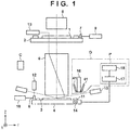
- Fig. 1 is a view showing the arrangement of an exposure apparatus to which the measurement apparatus of this present invention has been applied.
- directions are indicated based on an X-Y-Z coordinate system in which a direction parallel to the upper surface of a wafer 3 is set as an X-Y plane.
- an optical axis direction of a projection optical system 6 is a Z direction perpendicular to the X-Y plane.
- Directions parallel to an X-axis, a Y-axis, and a Z-axis are referred to as an X direction, a Y direction, and the Z direction, respectively.
- Reference symbols ⁇ X, ⁇ Y, and ⁇ Z represent a rotation about the X-axis, a rotation about the Y-axis, a rotation about the Z-axis, respectively.
- Control or driving related to the Z-axis, the Y-axis, and the Z-axis represent control or driving performed in relation to a direction parallel to the X-axis, a direction parallel to the Y-axis, and a direction parallel to the Z-axis, respectively.
- control or driving related to the ⁇ X-axis, the ⁇ Y-axis, and the ⁇ Z-axis represent control or driving performed in relation to a rotation about an axis parallel to the X-axis, a rotation about an axis parallel to the Y-axis, and a rotation about an axis parallel to the Z-axis, respectively.
- a position is information that can be specified based on the coordinates of the X-axis, the Y-axis, and the Z-axis
- an orientation is information that can be specified based on the values of the ⁇ X-axis, the ⁇ Y-axis, and the ⁇ Z-axis.
- Positioning represents controlling the position and/or the orientation. Alignment can include controlling a position and/or orientation of at least one of a substrate and an original.
- the exposure apparatus shown in Fig. 1 can be a scanning exposure apparatus (scanner) that projects and exposes a pattern formed on a reticle 1 onto the wafer 3 while moving the reticle 1 as an original (mask) and the wafer 3 as a substrate in the scanning direction.
- the exposure apparatus may be an exposure apparatus (stepper) that fixes the reticle and projects and exposes the pattern of the reticle 1 on the wafer 3.
- a reticle stage 2 can hold and move the reticle 1, and a wafer stage 4 can hold and move the wafer 3.
- An illumination optical system 5 illuminates the reticle 1 with exposure light.
- the projection optical system 6 projects a pattern image of the reticle 1, which has been illuminated by the exposure light, onto the wafer 3 held by the wafer stage 4.
- a controller C comprehensively controls the operation of the overall exposure apparatus.
- a mirror 7 is arranged on the reticle stage 2, and an X-Y direction laser interferometer 9 is arranged in a position which faces the mirror 7.
- the position and the rotational angle in the two-dimensional direction of the reticle 1 are measured by the laser interferometer 9 in real time, and the measurement results are output to the controller C.
- the controller C controls a driver of the reticle stage 2 based on the measurement result from the laser interferometer 9 to position the reticle 1 which is supported by the reticle stage 2.
- the wafer stage 4 includes a Z stage which holds the wafer 3 via a wafer chuck, an X-Y stage which supports the Z stage, and a base which supports the X-Y stage.
- a driver (not shown) such as a linear motor or the like drives the wafer stage 4.
- the controller C controls the driver of the wafer stage 4.
- a mirror 8 is arranged on the wafer stage 4.
- An X-Y direction laser interferometer 10 and a Z-direction laser interferometer 12 are arranged in positions that face the mirror 8. A position in the X-Y direction and the rotation ⁇ Z of the wafer stage 4 are measured by the laser interferometer 10 in real time, and the measurement results are output to the controller C.
- a position in the Z direction, the rotation ⁇ X, and the rotation ⁇ Y of the wafer stage 4 are measured by the laser interferometer 12 in real time, and the measurement results are output to the controller C.
- the controller C positions the wafer 3 supported by the wafer stage 4 by controlling the driver of the wafer stage 4 based on the measurement results from the laser interferometers 10 and 12 to drive the X-Y stage and the Z stage and adjust the position of the wafer 3 in the X, Y, and Z directions.
- a reticle alignment detector 13 adjusts the relative positional relationship between the reticle 1 and the wafer 3 by detecting a reference mark (not shown) on a reference plate 11 on the wafer stage 4 through the projection optical system 6 and a reference mark (not shown) on the reticle 1.
- a focus detector 15 includes a projection system that projects detection light to the surface of the wafer 3 and a light reception system that receives the reflected light from the wafer 3, and the detection result of the focus detector 15 is output to the controller C.
- the controller C drives the Z stage based on the detection result from the focus detector 15, and makes adjustments so that the tilt angle and the position (the height position, that is, the focus position) in the Z direction of the wafer 3 held on the Z stage will fall within permitted ranges.
- the exposure apparatus includes a measurement apparatus D that measures the position of a mark formed between a first surface (upper surface) of the substrate and a second surface (lower surface) on the opposite side of the first surface.
- the measurement apparatus D includes a wafer alignment detector 16 which is a first detector for detecting the image of a mark, an AF detector 41 (autofocus detector) which is a second detector for detecting the height position of the first surface of the substrate, and a processor P.
- the processor P can include a memory 17 and an input device 18.
- the wafer alignment detector 16 includes a projection system that projects detection light to a mark formed on the wafer 3 and a light reception system that receives the reflected light from the mark.
- the detection result of the wafer alignment detector 16 is output to the controller C.
- the controller C can adjust the position of the wafer 3 in the X-Y direction by driving the wafer stage 4 in the X-Y direction based on the detection result of the wafer alignment detector 16.
- the AF detector 41 detects a surface position of the wafer 3 to perform support to obtain the best focus position for the wafer alignment detector 16.
- the AF detector 41 includes, in the same manner as the focus detector 15, a projection system that projects detection light to the surface of the wafer 3 and a light reception system that receives the reflected light from the wafer 3. While the focus detector 15 is used for obtaining the best focus position for the projection optical system 6, the AF detector 41 is used for obtaining the best focus position for the wafer alignment detector 16.
- the AF detector 41 uses the projection system to obliquely project AF light to the wafer 3 and uses the AF detection sensor (not shown) of the light reception system to receive the reflected light from the wafer 3.
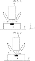
- Fig. 2 shows a state in which the AF detector 41 is performing focus measurement on the wafer 3 on which a mark 19 has been provided on the surface.
- the AF detector 41 can measure the height position of the wafer 3 based on the AF light reception position of the AF detection sensor. See Japanese Patent No. 6025346 for a more specific example of the arrangement of the wafer alignment detector 16 and the AF detector 41.
- the focus measurement operation by the AF detector 41 is performed not to measure the best focus position for mark detection by the wafer alignment detector 16, but to detect the surface position (the height position of the surface of the uppermost layer) of the wafer 3.
- the focus measurement operation by the AF detector 41 is measurement performed to make the mark image focus state of the wafer alignment detector 16 fall within the permitted range. Since the AF detector 41 detects the AF light reflected by the surface of the wafer 3, the AF detector 41 cannot directly detect the focus position of the mark arranged in the middle layer or on the lower surface of the wafer 3.
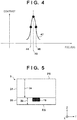
- An "image autofocus measurement” operation of obtaining the best focus position for the wafer alignment detector 16 to detect the mark 19 in a case in which the mark 19 is arranged on the upper surface of the wafer 3 will be described with reference to Fig. 3 .
- the AF detector 41 first detects the surface position of the wafer 3. The obtained surface position can be used to schematically match the focus position of the wafer alignment detector 16 with the mark 19. Subsequently, the mark 19 is irradiated with measurement light 22 from the wafer alignment detector 16.
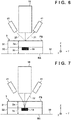
- the wafer alignment detector 16 obtains a contrast curve 47 as shown in Fig. 4 by calculating the contrast of the image of the mark 19 at each focus position while moving the wafer stage 4 in the Z direction.
- the contrast curve 47 shows the relationship between each focus position and the contrast.
- the wafer alignment detector 16 obtains, as the best focus position, a focus position at which the contrast is at the peak level in the contrast curve 47.
- the maximum contrast value it is possible to use a method using quadratic polynomial fitting, barycenter calculation, or the like on the obtained contrast curve. Note that although only three focus positions 44, 45, and 46 of the image autofocus measurement are shown for the sake of descriptive convenience, the measurement points may be increased to 10 points or 20 points. Note that it may be arranged so that this autofocus control will be performed by the controller C or be performed by the processor P. Assume that it is arranged so that the autofocus control is performed by the processor P in this case.
- the wafer 3 includes an upper layer 31 and a lower layer 32, and the mark 19 is covered by the upper layer 31.
- the lower layer 32 can be made of a glass support substrate
- the upper layer 31 can be made of an Si layer.
- Reference numeral 3a represents a distance (that is, the thickness of the upper layer 31) from an upper surface FS of the wafer 3 to the mark 19
- reference numeral 3b represents a distance (that is, the thickness of the lower layer 32) from the mark 19 to a lower surface RS of the wafer 3.
- the procedure of the image autofocus operation for measuring the position of the mark 19 is, for example, as follows. First, as shown in Fig. 6 , the AF detector 41 detects the height position of the upper surface of the wafer 3. Next, to obtain the best focus position of the mark 19, the starting point of the image autofocus measurement operation is determined by using the distance 3a and the refractive index of the material of the upper layer 31 (the layer extending from the upper surface FS to the mark 19). The starting point determination method will be described in detail hereinafter.
- the upper layer 31 is a Si layer having a thickness of 200 ⁇ m
- 200 ⁇ m/3.5 the refractive index of the Si layer
- the focus of the wafer alignment detector 16 can be set to the mark 19 as shown in Fig. 7 by driving the wafer stage by this offset amount OS top .
- infrared light or the like that can be transmitted through Si is used as the measurement light of the wafer alignment detector 16.
- the processor P determines the offset amount by obtaining a value by dividing the distance 3a from the surface of the wafer 3 to the mark by the refractive index of the upper layer 31 in this manner.
- the focus control process for adjusting the height of the stage to set the focus of the wafer alignment detector 16 to the mark is started.
- the processor P obtains the position of the mark based on the image of the mark detected by the wafer alignment detector 16.
- the measured value of the distance 3a from the upper surface FS of the wafer 3 to the mark 19 may vary among a plurality of substrates due to the influence from the process.
- the height position offset by the offset amount OS top in the manner described above becomes unsuitable as the starting position of the focus control operation, and the focus position search may require more time.
- the measured value of the distance 3b from the lower surface RS to the mark 19 may vary less among the plurality of substrates.
- the variation in the measured values of the distance 3b may be less than the variation in the measured values of the distance 3a in a case in which 3a > 3b or in a case in which lower layer 32 has a simple support substrate structure.
- it is possible to reduce the influence of the variation and determine the starting position of the image autofocus measurement operation by calculating an offset amount by using the second distance set as the distance 3b from the lower surface RS to the mark 19. Letting OS bottom be this amount, the offset amount OS bottom is expressed as follows. OS bottom total thickness of wafer ⁇ distance 3 b / refractive index of lower layer 32
- the height position of the upper surface of the wafer 3 can be detected by the AF detector 41.
- the height position of the lower surface RS can be obtained by using the AF detector 41 to measure the wafer support surface 30 in advance in a state without a wafer.
- the AF detector 41 can detect the height position of the surface of a wafer whose thickness is already known, and estimate the height position of the upper surface FS from the detection result.
- the processor P includes a first mode and a second mode in which the offset amount is determined differently from the first mode.
- the first mode an offset amount is determined based on the first distance set as a distance from the upper surface of the wafer to the mark.
- the second mode an offset amount is determined based on the second distance set as a distance from the lower surface of the wafer to the mark.
- a value obtained by dividing the first distance by a refractive index of the layer extending from the upper surface to the mark is determined to be the offset amount.
- a value obtained by dividing a value, which is obtained by subtracting the second distance from the total thickness (that is the distance between the upper surface and the lower surface of the wafer), by a refractive index of the layer extending from the upper surface to the mark is determined to be the offset amount.
- the distance (the thickness of the upper layer 31) from the upper surface FS to the mark 19 is input by the user via the input device 18, and this distance is set as the first distance.
- the refractive index of the upper layer 31 can be input via the input device 18.
- the distance (the thickness of the lower layer 32) from the mark 19 to the lower surface RS is input by the user via the input device 18, and this distance is set as the second distance.
- the refractive index of the lower layer 32 can be input via the input device 18.
- whether the distance 3a or the distance 3b is to be used can be selected in accordance with the set parameters.
- the processing operation can be performed by switching to the suitable processing (mode) in accordance with the process.
- each parameter may be input based on the process design information or set, to the apparatus via the network, based on a value measured by an external thickness measurement apparatus.
- a variation in measured values of a distance 3a and a variation in the measured values of a distance 3b can be obtained among a plurality of substrates, and a mode corresponding to the distance with less variation can be automatically selected among the first mode and the second mode.
- an image autofocus operation is performed on a plurality of wafers based on distance information and wafer refractive index information input to the apparatus in advance.
- Each measured value is obtained based on the height position of the upper surface of a wafer detected by an AF detector 41 and a result of a focus control process by a wafer alignment detector 16. That is, the actual values of the distance 3a and the distance 3b of each wafer are calculated from the height position of the surface of the wafer and the result of the image autofocus operation.
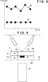
- Fig. 8 is a graph showing an example of a result obtained by plotting the measured values of the distance 3a and the distance 3b of each wafer.
- the variation amount between the wafers for each distance is calculated from this result.
- the first mode will be selected if the variation of the measured values of the distance 3a is less than the variation of the measured values of the distance 3b. Otherwise, the second mode will be selected.
- the starting position of the image autofocus operation is determined with high accuracy.
- a standard deviation, a dispersion value, or the like can be used as the variation amount between the wafers for each distance, the variation amount suffices to be an index representing the change ratio and is not limited to these examples.
- the measured value can be fed back to the distance information set in advance. For example, each time a first measured value which is the measured value of the distance 3a and a second measured value which is the measured value of the distance 3b are obtained, a processor P may update the first distance and the second distance stored in a memory 17 by the first measured value and the second measured value. As a result, it is possible to maintain accurate distance information based on an actual measurement.
- Fig. 9 shows an example of another arrangement of a wafer alignment detector 16.
- the wafer alignment detector 16 is arranged to detect an image of a mark through an upper surface FS of a wafer.
- the wafer alignment detector 16 is arranged to detect the image of the mark through a lower surface RS of the wafer.
- a mark 19 can be detected even in a case in which a layer through which infrared light cannot be transmitted is present between the upper surface FS and the mark 19.
- the wafer alignment detector 16 is arranged separately from the wafer stage, and the wafer stage can be driven to change the relative positions of the wafer and the wafer alignment detector 16.
- the focus position can be changed.
- the height position of the surface of the wafer calculated by an AF detector 41 and a distance 3b from the lower surface of the wafer to the mark are used to calculate the offset amount for the wafer alignment detector 16 to start the image autofocus operation.
- the image autofocus measurement operation of a mark 19 on the lower surface of a wafer 3 is performed at a high speed.
- an AF detector 41 detects the upper surface of the wafer.
- a processor P uses the height position of the upper surface of the wafer, which is detected by the AF detector 41, and the thickness information and the refractive index information of the wafer, which are set in advance, to calculate the offset amount for a wafer alignment detector 16 to start the image autofocus operation.
- the influence of the variation can be ignored by calculating the thickness of the wafer and using the calculated thickness each time.
- a value obtained by measuring the upper surface of the wafer support surface in advance by the AF detector 41 can be stored and used as the height position of the lower surface of the wafer.
- An article manufacturing method suitably manufactures an article, for example, a microdevice such as a semiconductor device or an element having a microstructure.
- the article manufacturing method of this embodiment includes a step of forming a latent pattern by using the above-described patterning method or lithography apparatus on a photosensitive agent applied on a substrate (an exposure step of exposing the substrate), and a development step of developing the substrate on which the latent pattern has been formed in the above step.
- the manufacturing method includes other well-known steps (for example, oxidation, film formation, deposition, doping, planarization, etching, resist removal, dicing, bonding, and packaging).
- the article manufacturing method of this embodiment is more advantageous than the conventional methods in at least one of the performance, quality, productivity, and production cost of the article.
Landscapes
- Physics & Mathematics (AREA)
- General Physics & Mathematics (AREA)
- Engineering & Computer Science (AREA)
- Multimedia (AREA)
- Chemical & Material Sciences (AREA)
- Life Sciences & Earth Sciences (AREA)
- Health & Medical Sciences (AREA)
- Analytical Chemistry (AREA)
- Biochemistry (AREA)
- General Health & Medical Sciences (AREA)
- Immunology (AREA)
- Pathology (AREA)
- Exposure And Positioning Against Photoresist Photosensitive Materials (AREA)
- Exposure Of Semiconductors, Excluding Electron Or Ion Beam Exposure (AREA)
- Length Measuring Devices By Optical Means (AREA)
Abstract
Description
- The present invention relates to a measurement apparatus, an exposure apparatus, and a method of manufacturing an article.
- In order to detect with high accuracy the position of a mark formed on a substrate, measurement needs to be performed in a focus position where the contrast is highest when an image of the mark is to be observed. However, in a measurement operation (image autofocus operation) that searches for a focus position where the contrast of a mark is highest, the search for the highest contrast position needs to be performed after performing mark observation and contrast calculation on a plurality of focus positions. Hence, the measurement operation takes time. Thus, there is a technique in which the speed of an image autofocus measurement operation is increased by using a substrate surface detection system capable of high-speed measurement to measure a focus position, which is to be a search starting point, in order to limit the search range of the image autofocus operation.
- For example, Japanese Patent No.
6025346 - In a multilayered substrate, a mark is arranged in a middle layer between the upper surface and the lower surface of a substrate, and the position of this mark needs to be measured. Normally, a design value is registered as the distance between the surface of the substrate and the mark. Although it is possible to use this registered design value for measurement, the actual distance will vary among a plurality of substrates. If there is a large variation, the starting point of an image autofocus operation which is determined based on the preset substrate thickness amount may become inappropriate. In such a case, the measurement time will increase due to the expansion of the search range in the image autofocus operation, and lead to throughput degradation.
- The present invention provides a measurement apparatus that is advantageous in both the accuracy and the throughput of substrate mark position measurement.
- The present invention in its first aspect provides a measurement apparatus as specified in
claims 1 to 11. - The present invention in its second aspect provides an exposure apparatus as specified in
claim 12. - The present invention in its third aspect provides a method of manufacturing an article as specified in
claim 13. - Further features of the present invention will become apparent from the following description of exemplary embodiments (with reference to the attached drawings).
-
-
Fig. 1 is a view showing the arrangement of an exposure apparatus according to this embodiment; -
Fig. 2 is a view for explaining an operation of an AF detector; -
Fig. 3 is a view for explaining an image autofocus measurement operation by a wafer alignment detector; -
Fig. 4 is a graph for explaining best focus position obtainment processing; -
Fig. 5 is a view showing an example of a substrate on which a mark is formed between an upper surface and a lower surface; -
Fig. 6 is a view for explaining an operation by the AF detector which is performed on the substrate on which the mark is formed between the upper surface and the lower surface; -
Fig. 7 is a view for explaining an offset driving operation of the wafer alignment detector; -
Fig. 8 is a graph showing an example of a result obtained by plotting measured values of layer thicknesses of respective wafers; -
Fig. 9 is a view showing an example of another arrangement of a wafer alignment detector; -
Fig. 10 is a view for explaining an offset driving operation of the wafer alignment detector in the example ofFig. 9 ; -
Fig. 11 is a view for explaining an operation by an AF detector performed on a substrate on which a mark has been formed on a lower surface; and -
Fig. 12 is a view for explaining an offset driving operation of a wafer alignment detector in the example ofFig. 11 . - Hereinafter, embodiments will be described in detail with reference to the attached drawings. Note, the following embodiments are not intended to limit the scope of the claimed invention. Multiple features are described in the embodiments, but limitation is not made an invention that requires all such features, and multiple such features may be combined as appropriate. Furthermore, in the attached drawings, the same reference numerals are given to the same or similar configurations, and redundant description thereof is omitted.
- A measurement apparatus of this present invention can be employed in, for example, an exposure apparatus used in a lithography process of a manufacturing process of an article such as a semiconductor device, liquid crystal display device, or the like, and can measure a surface position of a substrate.
Fig. 1 is a view showing the arrangement of an exposure apparatus to which the measurement apparatus of this present invention has been applied. In this specification and the accompanying drawings, directions are indicated based on an X-Y-Z coordinate system in which a direction parallel to the upper surface of awafer 3 is set as an X-Y plane. In this case, an optical axis direction of a projectionoptical system 6 is a Z direction perpendicular to the X-Y plane. Directions parallel to an X-axis, a Y-axis, and a Z-axis are referred to as an X direction, a Y direction, and the Z direction, respectively. Reference symbols θX, θY, and θZ represent a rotation about the X-axis, a rotation about the Y-axis, a rotation about the Z-axis, respectively. Control or driving related to the Z-axis, the Y-axis, and the Z-axis represent control or driving performed in relation to a direction parallel to the X-axis, a direction parallel to the Y-axis, and a direction parallel to the Z-axis, respectively. Also, control or driving related to the θX-axis, the θY-axis, and the θZ-axis represent control or driving performed in relation to a rotation about an axis parallel to the X-axis, a rotation about an axis parallel to the Y-axis, and a rotation about an axis parallel to the Z-axis, respectively. In addition, a position is information that can be specified based on the coordinates of the X-axis, the Y-axis, and the Z-axis, and an orientation is information that can be specified based on the values of the θX-axis, the θY-axis, and the θZ-axis. Positioning represents controlling the position and/or the orientation. Alignment can include controlling a position and/or orientation of at least one of a substrate and an original. - The exposure apparatus shown in
Fig. 1 can be a scanning exposure apparatus (scanner) that projects and exposes a pattern formed on areticle 1 onto thewafer 3 while moving thereticle 1 as an original (mask) and thewafer 3 as a substrate in the scanning direction. Alternatively, the exposure apparatus may be an exposure apparatus (stepper) that fixes the reticle and projects and exposes the pattern of thereticle 1 on thewafer 3. - A
reticle stage 2 can hold and move thereticle 1, and awafer stage 4 can hold and move thewafer 3. An illuminationoptical system 5 illuminates thereticle 1 with exposure light. The projectionoptical system 6 projects a pattern image of thereticle 1, which has been illuminated by the exposure light, onto thewafer 3 held by thewafer stage 4. A controller C comprehensively controls the operation of the overall exposure apparatus. - A
mirror 7 is arranged on thereticle stage 2, and an X-Y direction laser interferometer 9 is arranged in a position which faces themirror 7. The position and the rotational angle in the two-dimensional direction of thereticle 1 are measured by the laser interferometer 9 in real time, and the measurement results are output to the controller C. The controller C controls a driver of thereticle stage 2 based on the measurement result from the laser interferometer 9 to position thereticle 1 which is supported by thereticle stage 2. - The
wafer stage 4 includes a Z stage which holds thewafer 3 via a wafer chuck, an X-Y stage which supports the Z stage, and a base which supports the X-Y stage. A driver (not shown) such as a linear motor or the like drives thewafer stage 4. The controller C controls the driver of thewafer stage 4. Amirror 8 is arranged on thewafer stage 4. An X-Ydirection laser interferometer 10 and a Z-direction laser interferometer 12 are arranged in positions that face themirror 8. A position in the X-Y direction and the rotation θZ of thewafer stage 4 are measured by thelaser interferometer 10 in real time, and the measurement results are output to the controller C. A position in the Z direction, the rotation θX, and the rotation θY of thewafer stage 4 are measured by thelaser interferometer 12 in real time, and the measurement results are output to the controller C. The controller C positions thewafer 3 supported by thewafer stage 4 by controlling the driver of thewafer stage 4 based on the measurement results from thelaser interferometers wafer 3 in the X, Y, and Z directions. - A
reticle alignment detector 13 adjusts the relative positional relationship between thereticle 1 and thewafer 3 by detecting a reference mark (not shown) on areference plate 11 on thewafer stage 4 through the projectionoptical system 6 and a reference mark (not shown) on thereticle 1. Afocus detector 15 includes a projection system that projects detection light to the surface of thewafer 3 and a light reception system that receives the reflected light from thewafer 3, and the detection result of thefocus detector 15 is output to the controller C. The controller C drives the Z stage based on the detection result from thefocus detector 15, and makes adjustments so that the tilt angle and the position (the height position, that is, the focus position) in the Z direction of thewafer 3 held on the Z stage will fall within permitted ranges. - The exposure apparatus includes a measurement apparatus D that measures the position of a mark formed between a first surface (upper surface) of the substrate and a second surface (lower surface) on the opposite side of the first surface. The measurement apparatus D includes a
wafer alignment detector 16 which is a first detector for detecting the image of a mark, an AF detector 41 (autofocus detector) which is a second detector for detecting the height position of the first surface of the substrate, and a processor P. The processor P can include amemory 17 and aninput device 18. - The
wafer alignment detector 16 includes a projection system that projects detection light to a mark formed on thewafer 3 and a light reception system that receives the reflected light from the mark. The detection result of thewafer alignment detector 16 is output to the controller C. The controller C can adjust the position of thewafer 3 in the X-Y direction by driving thewafer stage 4 in the X-Y direction based on the detection result of thewafer alignment detector 16. - The
AF detector 41 detects a surface position of thewafer 3 to perform support to obtain the best focus position for thewafer alignment detector 16. TheAF detector 41 includes, in the same manner as thefocus detector 15, a projection system that projects detection light to the surface of thewafer 3 and a light reception system that receives the reflected light from thewafer 3. While thefocus detector 15 is used for obtaining the best focus position for the projectionoptical system 6, theAF detector 41 is used for obtaining the best focus position for thewafer alignment detector 16. - The
AF detector 41 uses the projection system to obliquely project AF light to thewafer 3 and uses the AF detection sensor (not shown) of the light reception system to receive the reflected light from thewafer 3.Fig. 2 shows a state in which theAF detector 41 is performing focus measurement on thewafer 3 on which amark 19 has been provided on the surface. When thewafer 3 moves in the focus direction (Z direction), the AF light reception position of the AF detection sensor shifts in accordance with the movement. Hence, theAF detector 41 can measure the height position of thewafer 3 based on the AF light reception position of the AF detection sensor. See Japanese Patent No.6025346 wafer alignment detector 16 and theAF detector 41. - The focus measurement operation by the
AF detector 41 is performed not to measure the best focus position for mark detection by thewafer alignment detector 16, but to detect the surface position (the height position of the surface of the uppermost layer) of thewafer 3. The focus measurement operation by theAF detector 41 is measurement performed to make the mark image focus state of thewafer alignment detector 16 fall within the permitted range. Since theAF detector 41 detects the AF light reflected by the surface of thewafer 3, theAF detector 41 cannot directly detect the focus position of the mark arranged in the middle layer or on the lower surface of thewafer 3. - An "image autofocus measurement" operation of obtaining the best focus position for the
wafer alignment detector 16 to detect themark 19 in a case in which themark 19 is arranged on the upper surface of thewafer 3 will be described with reference toFig. 3 . In the image autofocus measurement operation, theAF detector 41 first detects the surface position of thewafer 3. The obtained surface position can be used to schematically match the focus position of thewafer alignment detector 16 with themark 19. Subsequently, themark 19 is irradiated withmeasurement light 22 from thewafer alignment detector 16. - Although the focus of the
AF detector 41 is generally set to themark 19 arranged on the surface of thewafer 3, a focus position at which the contrast of the image of themark 19 becomes highest needs to be obtained for thewafer alignment detector 16 to perform alignment with high accuracy. Hence, thewafer alignment detector 16 obtains acontrast curve 47 as shown inFig. 4 by calculating the contrast of the image of themark 19 at each focus position while moving thewafer stage 4 in the Z direction. Thecontrast curve 47 shows the relationship between each focus position and the contrast. Thewafer alignment detector 16 obtains, as the best focus position, a focus position at which the contrast is at the peak level in thecontrast curve 47. To calculate the maximum contrast value, it is possible to use a method using quadratic polynomial fitting, barycenter calculation, or the like on the obtained contrast curve. Note that although only threefocus positions - The image autofocus measurement operation of a case in which the
mark 19 is arranged between the upper surface (first surface) and the lower surface (second surface) of thewafer 3 will be described with reference toFigs. 5 ,6, and 7 . InFig. 5 , thewafer 3 includes anupper layer 31 and alower layer 32, and themark 19 is covered by theupper layer 31. For example, thelower layer 32 can be made of a glass support substrate, and theupper layer 31 can be made of an Si layer.Reference numeral 3a represents a distance (that is, the thickness of the upper layer 31) from an upper surface FS of thewafer 3 to themark 19, and reference numeral 3b represents a distance (that is, the thickness of the lower layer 32) from themark 19 to a lower surface RS of thewafer 3. - The procedure of the image autofocus operation for measuring the position of the
mark 19 is, for example, as follows. First, as shown inFig. 6 , theAF detector 41 detects the height position of the upper surface of thewafer 3. Next, to obtain the best focus position of themark 19, the starting point of the image autofocus measurement operation is determined by using thedistance 3a and the refractive index of the material of the upper layer 31 (the layer extending from the upper surface FS to the mark 19). The starting point determination method will be described in detail hereinafter. - The processor P determines, from the height position of the upper surface FS of the
wafer 3 detected by theAF detector 41, the offset amount for adjusting the focus of thewafer alignment detector 16 on themark 19. For example, thedistance 3a (the thickness of the upper layer 31) from the upper surface FS to themark 19 is input by a user via theinput device 18, and thisdistance 3a is set as the first distance. In addition, the refractive index of theupper layer 31 can be input via theinput device 18. These sets of input data are stored in thememory 17. The processor P determines, based on thedistance 3a and the refractive index of theupper layer 31, the offset amount for adjusting the focus ofwafer alignment detector 16 on themark 19, and instructs thewafer stage 4 to be driven by the determined offset amount. An offset amount OStop in this case is expressed as follows.
- For example, in a case in which the
upper layer 31 is a Si layer having a thickness of 200 µm, 200 µm/3.5 (the refractive index of the Si layer) ≈ 57 µm. The focus of thewafer alignment detector 16 can be set to themark 19 as shown inFig. 7 by driving the wafer stage by this offset amount OStop. Note that infrared light or the like that can be transmitted through Si is used as the measurement light of thewafer alignment detector 16. The processor P determines the offset amount by obtaining a value by dividing thedistance 3a from the surface of thewafer 3 to the mark by the refractive index of theupper layer 31 in this manner. Subsequently, after the stage is moved to a height position offset by this offset amount, the focus control process for adjusting the height of the stage to set the focus of thewafer alignment detector 16 to the mark is started. As a result, rapid measurement can be performed. After the focus control process, the processor P obtains the position of the mark based on the image of the mark detected by thewafer alignment detector 16. - However, in the case of a bonded substrate as shown in
Fig. 5 , the measured value of thedistance 3a from the upper surface FS of thewafer 3 to themark 19 may vary among a plurality of substrates due to the influence from the process. As a result, the height position offset by the offset amount OStop in the manner described above becomes unsuitable as the starting position of the focus control operation, and the focus position search may require more time. In this case, depending on the process, the measured value of thedistance 3b from the lower surface RS to themark 19 may vary less among the plurality of substrates. For example, the variation in the measured values of thedistance 3b may be less than the variation in the measured values of thedistance 3a in a case in which 3a > 3b or in a case in whichlower layer 32 has a simple support substrate structure. In such a case, it is possible to reduce the influence of the variation and determine the starting position of the image autofocus measurement operation by calculating an offset amount by using the second distance set as thedistance 3b from the lower surface RS to themark 19. Letting OSbottom be this amount, the offset amount OSbottom is expressed as follows.
- Note that the total thickness of the wafer can be calculated from the difference between the height position of the upper surface FS and the height position of the lower surface RS (= a wafer support surface 30) of the
wafer 3. The height position of the upper surface of thewafer 3 can be detected by theAF detector 41. The height position of the lower surface RS can be obtained by using theAF detector 41 to measure thewafer support surface 30 in advance in a state without a wafer. Alternatively, theAF detector 41 can detect the height position of the surface of a wafer whose thickness is already known, and estimate the height position of the upper surface FS from the detection result. - As described above, in this embodiment, the processor P includes a first mode and a second mode in which the offset amount is determined differently from the first mode. In the first mode, an offset amount is determined based on the first distance set as a distance from the upper surface of the wafer to the mark. In the second mode, an offset amount is determined based on the second distance set as a distance from the lower surface of the wafer to the mark.
- In the first mode, in accordance with equation (1) described above, a value obtained by dividing the first distance by a refractive index of the layer extending from the upper surface to the mark is determined to be the offset amount. In the second mode, in accordance with equation (2), a value obtained by dividing a value, which is obtained by subtracting the second distance from the total thickness (that is the distance between the upper surface and the lower surface of the wafer), by a refractive index of the layer extending from the upper surface to the mark is determined to be the offset amount.
- For example, the distance (the thickness of the upper layer 31) from the upper surface FS to the
mark 19 is input by the user via theinput device 18, and this distance is set as the first distance. Also, the refractive index of theupper layer 31 can be input via theinput device 18. In a similar manner, the distance (the thickness of the lower layer 32) from themark 19 to the lower surface RS is input by the user via theinput device 18, and this distance is set as the second distance. Also, the refractive index of thelower layer 32 can be input via theinput device 18. These sets of input data are stored in thememory 17. Hence, by selecting and using, among thedistance 3a and thedistance 3b, the value of the distance with less variation among the plurality of wafers, it becomes possible to calculate the starting point of the image autofocus operation with reduced influence of the variation. As a result, it becomes possible to increase the speed of the measurement operation (that is, improve throughput) while maintaining the accuracy of the measurement of the position of the mark. - In this embodiment, whether the
distance 3a or thedistance 3b is to be used, that is, whether the first mode or the second mode is to be used can be selected in accordance with the set parameters. As a result, the processing operation can be performed by switching to the suitable processing (mode) in accordance with the process. Note that each parameter may be input based on the process design information or set, to the apparatus via the network, based on a value measured by an external thickness measurement apparatus. - For example, a variation in measured values of a
distance 3a and a variation in the measured values of adistance 3b can be obtained among a plurality of substrates, and a mode corresponding to the distance with less variation can be automatically selected among the first mode and the second mode. - In this embodiment, an image autofocus operation is performed on a plurality of wafers based on distance information and wafer refractive index information input to the apparatus in advance. Each measured value is obtained based on the height position of the upper surface of a wafer detected by an
AF detector 41 and a result of a focus control process by awafer alignment detector 16. That is, the actual values of thedistance 3a and thedistance 3b of each wafer are calculated from the height position of the surface of the wafer and the result of the image autofocus operation. -
Fig. 8 is a graph showing an example of a result obtained by plotting the measured values of thedistance 3a and thedistance 3b of each wafer. The variation amount between the wafers for each distance is calculated from this result. In this case, for example, the first mode will be selected if the variation of the measured values of thedistance 3a is less than the variation of the measured values of thedistance 3b. Otherwise, the second mode will be selected. As a result, the starting position of the image autofocus operation is determined with high accuracy. Note that although a standard deviation, a dispersion value, or the like can be used as the variation amount between the wafers for each distance, the variation amount suffices to be an index representing the change ratio and is not limited to these examples. - In addition, the measured value can be fed back to the distance information set in advance. For example, each time a first measured value which is the measured value of the
distance 3a and a second measured value which is the measured value of thedistance 3b are obtained, a processor P may update the first distance and the second distance stored in amemory 17 by the first measured value and the second measured value. As a result, it is possible to maintain accurate distance information based on an actual measurement. -
Fig. 9 shows an example of another arrangement of awafer alignment detector 16. In the example ofFig. 6 , thewafer alignment detector 16 is arranged to detect an image of a mark through an upper surface FS of a wafer. In contrast, inFig. 9 , thewafer alignment detector 16 is arranged to detect the image of the mark through a lower surface RS of the wafer. As a result, amark 19 can be detected even in a case in which a layer through which infrared light cannot be transmitted is present between the upper surface FS and themark 19. In this case, thewafer alignment detector 16 is arranged separately from the wafer stage, and the wafer stage can be driven to change the relative positions of the wafer and thewafer alignment detector 16. As a result, the focus position can be changed. In this arrangement, the height position of the surface of the wafer calculated by anAF detector 41 and adistance 3b from the lower surface of the wafer to the mark are used to calculate the offset amount for thewafer alignment detector 16 to start the image autofocus operation. This offset amount OSbottom is expressed as follows.
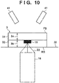
- As a result, as shown in
Fig. 10 , it is possible to determine, with respect to themark 19 inside awafer 3, the starting point of the image autofocus operation of thewafer alignment detector 16, which is arranged on the side of the lower surface of the wafer. Also, in a case in which the variation ofdistance 3a is less than that of thedistance 3b in a manner similar to the first embodiment, the offset amount OSbottom can be calculated as follows.
- Note that an arrangement in which a value corresponding to the distance with the less variation among the plurality of wafers, which is the arrangement of the second embodiment, may be combined with and applied to the arrangement according to this embodiment.
- In the fourth embodiment, the image autofocus measurement operation of a
mark 19 on the lower surface of awafer 3 is performed at a high speed. As shown inFig. 11 , anAF detector 41 detects the upper surface of the wafer. A processor P uses the height position of the upper surface of the wafer, which is detected by theAF detector 41, and the thickness information and the refractive index information of the wafer, which are set in advance, to calculate the offset amount for awafer alignment detector 16 to start the image autofocus operation. An offset amount OS is calculated as follows.
- Note that the "thickness of wafer" can be calculated from the difference between the height position of the upper surface of the wafer detected by the
AF detector 41 and the height position of the lower surface (= a wafer support surface) of the wafer. As a result, even in a case in which there is variation in the "thickness of wafer", the influence of the variation can be ignored by calculating the thickness of the wafer and using the calculated thickness each time. In this manner, as shown inFig. 12 , it is possible to accurately determine the starting point of the image autofocus operation to be performed on themark 19 on the lower surface of thewafer 3 by thewafer alignment detector 16. Note that a value obtained by measuring the upper surface of the wafer support surface in advance by theAF detector 41 can be stored and used as the height position of the lower surface of the wafer. - An article manufacturing method according to an embodiment of the present invention suitably manufactures an article, for example, a microdevice such as a semiconductor device or an element having a microstructure. The article manufacturing method of this embodiment includes a step of forming a latent pattern by using the above-described patterning method or lithography apparatus on a photosensitive agent applied on a substrate (an exposure step of exposing the substrate), and a development step of developing the substrate on which the latent pattern has been formed in the above step. In addition, the manufacturing method includes other well-known steps (for example, oxidation, film formation, deposition, doping, planarization, etching, resist removal, dicing, bonding, and packaging). The article manufacturing method of this embodiment is more advantageous than the conventional methods in at least one of the performance, quality, productivity, and production cost of the article.
- The present invention is not limited to the above-described embodiments, and various changes and modifications can be made within the spirit and scope of the present invention. Therefore, to apprise the public of the scope of the present invention, the following claims are made.
- While the present invention has been described with reference to exemplary embodiments, it is to be understood that the invention is not limited to the disclosed exemplary embodiments. The scope of the following claims is to be accorded the broadest interpretation so as to encompass all such modifications and equivalent structures and functions.
Claims (13)
- A measurement apparatus that measures a position of a mark (19) formed between a first surface and a second surface on a side opposite to the first surface of a substrate (3), characterized by comprising:a stage (4) configured to hold and move the substrate;a first detector (16) configured to detect an image of the mark;a second detector (41) configured to detect a height position of the first surface; anda processor (P) configured to determine, based on the height position of the first surface detected by the second detector, an offset amount used to set the focus of the first detector to the mark,wherein the processor includes a first mode in which the offset amount is determined based on a first distance set as a distance from the first surface to the mark, and a second mode in which the offset amount is determined based on a second distance set as a distance from the second surface to the mark.
- The apparatus according to claim 1, characterized in that in the first mode, the processor determines, as the offset amount, an amount obtained by dividing the first distance by a refractive index of a layer extending from the first surface to the mark, and in the second mode, the processor determines, as the offset amount, a value obtained by dividing a value, which is obtained by subtracting the second distance from a distance between the first surface and the second surface, by the refractive index.
- The apparatus according to claim 1, characterized in that the processor performs a focus control process in which a height of the stage is adjusted so as to set the focus of the first detector to the mark after moving the stage to a height position that has been offset by the offset amount, and the processor obtains the position of the mark based on the image of the mark detected by the first detector after the focus control process.
- The apparatus according to claim 3, characterized in that the processor selects the first mode in a case in which a variation in measured values of the distance between the first surface and the mark is less than a variation in measured values of the distance between the second surface and the mark among a plurality of substrates, and otherwise, the processor selects the second mode.
- The apparatus according to claim 4, characterized in that the processor obtains the measured value based on the height position of the first surface detected by the second detector and a result of the focus control process.
- The apparatus according to claim 5, characterized by further comprising:a memory (17) configured to store the first distance and the second distance,wherein each time a first measured value which is a measured value of the distance between the first surface and the mark and a second measured value which is a measured value of the distance between the second surface and the mark are obtained, the processor updates the first distance and the second distance stored in the memory by the first measured value and the second measured value, respectively.
- The apparatus according to any one of claims 1 to 6, characterized in that the first detector is arranged so as to detect the image of the mark through the first surface.
- The apparatus according to any one of claims 1 to 6, characterized in that the first detector is arranged so as to detect the image of the mark through the second surface.
- The apparatus according to any one of claims 1 to 8, characterized by further comprising:
an input device (18) for a user to select the first mode or the second mode. - The apparatus according to any one of claims 1 to 9, characterized in that the second detector obliquely projects light to the first surface and detects the light reflected by the first surface to detect the height position of the first surface.
- The apparatus according to claim 4, characterized in that in the focus control process, the processor obtains a contrast curve of the image of the mark by detecting the image of the mark by the first detector while moving the stage from a starting point which is set at a height position that has been offset by the offset amount, and the processor obtains, as a best focus position, a height position at which the contrast is at a peak level in the contrast curve.
- An exposure apparatus that exposes a substrate, characterized by comprising:a measurement apparatus defined in any one of claims 1 to 11; anda controller configured to control the stage based on a position of a mark on the substrate measured by the measurement apparatus.
- A method of manufacturing an article, characterized by comprising:exposing a substrate by using an exposure apparatus defined in claim 12;developing the exposed substrate; andmanufacturing the article from the developed substrate.
Applications Claiming Priority (1)
| Application Number | Priority Date | Filing Date | Title |
|---|---|---|---|
| JP2019024696A JP7173891B2 (en) | 2019-02-14 | 2019-02-14 | Measuring device, exposure device, and article manufacturing method |
Publications (2)
| Publication Number | Publication Date |
|---|---|
| EP3696608A1 true EP3696608A1 (en) | 2020-08-19 |
| EP3696608B1 EP3696608B1 (en) | 2024-07-10 |
Family
ID=69423198
Family Applications (1)
| Application Number | Title | Priority Date | Filing Date |
|---|---|---|---|
| EP20154931.8A Active EP3696608B1 (en) | 2019-02-14 | 2020-01-31 | Measurement apparatus, exposure apparatus, and method of manufacturing article |
Country Status (3)
| Country | Link |
|---|---|
| US (1) | US11067908B2 (en) |
| EP (1) | EP3696608B1 (en) |
| JP (1) | JP7173891B2 (en) |
Families Citing this family (2)
| Publication number | Priority date | Publication date | Assignee | Title |
|---|---|---|---|---|
| EP3667423B1 (en) * | 2018-11-30 | 2024-04-03 | Canon Kabushiki Kaisha | Lithography apparatus, determination method, and method of manufacturing an article |
| US12529556B2 (en) | 2020-09-10 | 2026-01-20 | Tokyo Electron Limited | Thickness measuring device and thickness measuring method to measure thickness of substrate |
Citations (4)
| Publication number | Priority date | Publication date | Assignee | Title |
|---|---|---|---|---|
| JPS6025346B2 (en) | 1977-09-09 | 1985-06-18 | キヤノン株式会社 | Control method for paper feeding devices such as copying machines |
| JP2005005444A (en) * | 2003-06-11 | 2005-01-06 | Nikon Corp | Alignment apparatus, exposure apparatus, alignment method, exposure method, and position information detection method |
| US20090237635A1 (en) * | 2008-03-12 | 2009-09-24 | Asml Netherlands B.V. | Lithographic apparatus and method |
| EP2722714A2 (en) * | 2012-10-19 | 2014-04-23 | Canon Kabushiki Kaisha | Detection device, exposure apparatus and device manufacturing method using such an exposure apparatus |
Family Cites Families (13)
| Publication number | Priority date | Publication date | Assignee | Title |
|---|---|---|---|---|
| NL9100410A (en) * | 1991-03-07 | 1992-10-01 | Asm Lithography Bv | IMAGE DEVICE EQUIPPED WITH A FOCUS ERROR AND / OR TILT DETECTION DEVICE. |
| JPH09326351A (en) * | 1996-06-03 | 1997-12-16 | Nikon Corp | Surface position adjustment device |
| JP2010263005A (en) * | 2009-04-30 | 2010-11-18 | Canon Inc | Exposure equipment |
| JP5162006B2 (en) * | 2011-06-01 | 2013-03-13 | キヤノン株式会社 | Detection apparatus, exposure apparatus, and device manufacturing method |
| JP5556774B2 (en) * | 2011-09-16 | 2014-07-23 | ウシオ電機株式会社 | Exposure equipment |
| JP6025346B2 (en) * | 2012-03-05 | 2016-11-16 | キヤノン株式会社 | Detection apparatus, exposure apparatus, and device manufacturing method |
| JP5984459B2 (en) * | 2012-03-30 | 2016-09-06 | キヤノン株式会社 | Exposure apparatus, exposure apparatus control method, and device manufacturing method |
| JP5743958B2 (en) * | 2012-05-30 | 2015-07-01 | キヤノン株式会社 | Measuring method, exposure method and apparatus |
| JP6366261B2 (en) * | 2013-12-05 | 2018-08-01 | キヤノン株式会社 | Lithographic apparatus and article manufacturing method |
| US9958257B2 (en) * | 2015-09-21 | 2018-05-01 | Kla-Tencor Corporation | Increasing dynamic range of a height sensor for inspection and metrology |
| JP6207671B1 (en) * | 2016-06-01 | 2017-10-04 | キヤノン株式会社 | Pattern forming apparatus, substrate arranging method, and article manufacturing method |
| US10788765B2 (en) * | 2017-01-25 | 2020-09-29 | Asml Netherlands B.V. | Method and apparatus for measuring a structure on a substrate |
| JP7328809B2 (en) * | 2019-07-01 | 2023-08-17 | キヤノン株式会社 | DETECTION DEVICE, EXPOSURE DEVICE, AND ARTICLE MANUFACTURING METHOD |
-
2019
- 2019-02-14 JP JP2019024696A patent/JP7173891B2/en active Active
-
2020
- 2020-01-31 EP EP20154931.8A patent/EP3696608B1/en active Active
- 2020-02-11 US US16/787,174 patent/US11067908B2/en active Active
Patent Citations (4)
| Publication number | Priority date | Publication date | Assignee | Title |
|---|---|---|---|---|
| JPS6025346B2 (en) | 1977-09-09 | 1985-06-18 | キヤノン株式会社 | Control method for paper feeding devices such as copying machines |
| JP2005005444A (en) * | 2003-06-11 | 2005-01-06 | Nikon Corp | Alignment apparatus, exposure apparatus, alignment method, exposure method, and position information detection method |
| US20090237635A1 (en) * | 2008-03-12 | 2009-09-24 | Asml Netherlands B.V. | Lithographic apparatus and method |
| EP2722714A2 (en) * | 2012-10-19 | 2014-04-23 | Canon Kabushiki Kaisha | Detection device, exposure apparatus and device manufacturing method using such an exposure apparatus |
Also Published As
| Publication number | Publication date |
|---|---|
| EP3696608B1 (en) | 2024-07-10 |
| JP7173891B2 (en) | 2022-11-16 |
| JP2020134587A (en) | 2020-08-31 |
| US20200264524A1 (en) | 2020-08-20 |
| US11067908B2 (en) | 2021-07-20 |
Similar Documents
| Publication | Publication Date | Title |
|---|---|---|
| US5917580A (en) | Scan exposure method and apparatus | |
| US6292254B1 (en) | Projection exposure method and apparatus | |
| JP4434372B2 (en) | Projection exposure apparatus and device manufacturing method | |
| KR102354948B1 (en) | Exposure apparatus, and method of manufacturing article | |
| KR102222673B1 (en) | Exposure apparatus and method of manufacturing article | |
| EP3696608B1 (en) | Measurement apparatus, exposure apparatus, and method of manufacturing article | |
| KR20080096433A (en) | Exposure apparatus and device manufacturing method | |
| US10488764B2 (en) | Lithography apparatus, lithography method, and method of manufacturing article | |
| KR20130111423A (en) | Exposure apparatus, method of controlling the same and method of manufacturing device | |
| JP2010087310A (en) | Exposure apparatus, and method of manufacturing device | |
| JPH11186129A (en) | Scanning exposure method and apparatus | |
| JP6399739B2 (en) | Exposure apparatus, exposure method, and device manufacturing method | |
| US6940586B2 (en) | Exposure apparatus and method | |
| US6750950B1 (en) | Scanning exposure method, scanning exposure apparatus and making method for producing the same, and device and method for manufacturing the same | |
| JP2019152685A (en) | Exposure device, exposure method, and article manufacturing method | |
| KR20220088332A (en) | Measurement apparatus, exposure apparatus, and article manufacturing method | |
| JP2010283157A (en) | Exposure apparatus and device manufacturing method | |
| KR20200049538A (en) | Stage apparatus, lithography apparatus, and article manufacturing method | |
| JPH10261567A (en) | Projection exposure apparatus and method for measuring optical characteristics of projection optical system | |
| JP2021026113A (en) | Exposure apparatus and article manufacturing method | |
| KR102824961B1 (en) | Information processing apparatus, information processing method, program, exposure apparatus, exposure method, and article manufacturing method | |
| JPH09293660A (en) | Projection exposure equipment | |
| JP7022611B2 (en) | Exposure device control method, exposure device, and article manufacturing method | |
| JP2023077924A (en) | Exposure apparatus, exposure method, and article manufacturing method | |
| JP2024066628A (en) | Exposure apparatus, exposure method, and method for manufacturing article |
Legal Events
| Date | Code | Title | Description |
|---|---|---|---|
| PUAI | Public reference made under article 153(3) epc to a published international application that has entered the european phase |
Free format text: ORIGINAL CODE: 0009012 |
|
| STAA | Information on the status of an ep patent application or granted ep patent |
Free format text: STATUS: THE APPLICATION HAS BEEN PUBLISHED |
|
| AK | Designated contracting states |
Kind code of ref document: A1 Designated state(s): AL AT BE BG CH CY CZ DE DK EE ES FI FR GB GR HR HU IE IS IT LI LT LU LV MC MK MT NL NO PL PT RO RS SE SI SK SM TR |
|
| AX | Request for extension of the european patent |
Extension state: BA ME |
|
| STAA | Information on the status of an ep patent application or granted ep patent |
Free format text: STATUS: REQUEST FOR EXAMINATION WAS MADE |
|
| 17P | Request for examination filed |
Effective date: 20210219 |
|
| RBV | Designated contracting states (corrected) |
Designated state(s): AL AT BE BG CH CY CZ DE DK EE ES FI FR GB GR HR HU IE IS IT LI LT LU LV MC MK MT NL NO PL PT RO RS SE SI SK SM TR |
|
| GRAP | Despatch of communication of intention to grant a patent |
Free format text: ORIGINAL CODE: EPIDOSNIGR1 |
|
| STAA | Information on the status of an ep patent application or granted ep patent |
Free format text: STATUS: GRANT OF PATENT IS INTENDED |
|
| INTG | Intention to grant announced |
Effective date: 20240220 |
|
| GRAS | Grant fee paid |
Free format text: ORIGINAL CODE: EPIDOSNIGR3 |
|
| GRAA | (expected) grant |
Free format text: ORIGINAL CODE: 0009210 |
|
| STAA | Information on the status of an ep patent application or granted ep patent |
Free format text: STATUS: THE PATENT HAS BEEN GRANTED |
|
| AK | Designated contracting states |
Kind code of ref document: B1 Designated state(s): AL AT BE BG CH CY CZ DE DK EE ES FI FR GB GR HR HU IE IS IT LI LT LU LV MC MK MT NL NO PL PT RO RS SE SI SK SM TR |
|
| REG | Reference to a national code |
Ref country code: CH Ref legal event code: EP |
|
| REG | Reference to a national code |
Ref country code: DE Ref legal event code: R096 Ref document number: 602020033595 Country of ref document: DE |
|
| REG | Reference to a national code |
Ref country code: LT Ref legal event code: MG9D |
|
| REG | Reference to a national code |
Ref country code: NL Ref legal event code: MP Effective date: 20240710 |
|
| PG25 | Lapsed in a contracting state [announced via postgrant information from national office to epo] |
Ref country code: PT Free format text: LAPSE BECAUSE OF FAILURE TO SUBMIT A TRANSLATION OF THE DESCRIPTION OR TO PAY THE FEE WITHIN THE PRESCRIBED TIME-LIMIT Effective date: 20241111 |
|
| REG | Reference to a national code |
Ref country code: AT Ref legal event code: MK05 Ref document number: 1702571 Country of ref document: AT Kind code of ref document: T Effective date: 20240710 |
|
| PG25 | Lapsed in a contracting state [announced via postgrant information from national office to epo] |
Ref country code: NL Free format text: LAPSE BECAUSE OF FAILURE TO SUBMIT A TRANSLATION OF THE DESCRIPTION OR TO PAY THE FEE WITHIN THE PRESCRIBED TIME-LIMIT Effective date: 20240710 |
|
| PG25 | Lapsed in a contracting state [announced via postgrant information from national office to epo] |
Ref country code: PT Free format text: LAPSE BECAUSE OF FAILURE TO SUBMIT A TRANSLATION OF THE DESCRIPTION OR TO PAY THE FEE WITHIN THE PRESCRIBED TIME-LIMIT Effective date: 20241111 Ref country code: NL Free format text: LAPSE BECAUSE OF FAILURE TO SUBMIT A TRANSLATION OF THE DESCRIPTION OR TO PAY THE FEE WITHIN THE PRESCRIBED TIME-LIMIT Effective date: 20240710 |
|
| PG25 | Lapsed in a contracting state [announced via postgrant information from national office to epo] |
Ref country code: NO Free format text: LAPSE BECAUSE OF FAILURE TO SUBMIT A TRANSLATION OF THE DESCRIPTION OR TO PAY THE FEE WITHIN THE PRESCRIBED TIME-LIMIT Effective date: 20241010 |
|
| PG25 | Lapsed in a contracting state [announced via postgrant information from national office to epo] |
Ref country code: PL Free format text: LAPSE BECAUSE OF FAILURE TO SUBMIT A TRANSLATION OF THE DESCRIPTION OR TO PAY THE FEE WITHIN THE PRESCRIBED TIME-LIMIT Effective date: 20240710 Ref country code: GR Free format text: LAPSE BECAUSE OF FAILURE TO SUBMIT A TRANSLATION OF THE DESCRIPTION OR TO PAY THE FEE WITHIN THE PRESCRIBED TIME-LIMIT Effective date: 20241011 Ref country code: FI Free format text: LAPSE BECAUSE OF FAILURE TO SUBMIT A TRANSLATION OF THE DESCRIPTION OR TO PAY THE FEE WITHIN THE PRESCRIBED TIME-LIMIT Effective date: 20240710 |
|
| PG25 | Lapsed in a contracting state [announced via postgrant information from national office to epo] |
Ref country code: BG Free format text: LAPSE BECAUSE OF FAILURE TO SUBMIT A TRANSLATION OF THE DESCRIPTION OR TO PAY THE FEE WITHIN THE PRESCRIBED TIME-LIMIT Effective date: 20240710 |
|
| PG25 | Lapsed in a contracting state [announced via postgrant information from national office to epo] |
Ref country code: LV Free format text: LAPSE BECAUSE OF FAILURE TO SUBMIT A TRANSLATION OF THE DESCRIPTION OR TO PAY THE FEE WITHIN THE PRESCRIBED TIME-LIMIT Effective date: 20240710 |
|
| PG25 | Lapsed in a contracting state [announced via postgrant information from national office to epo] |
Ref country code: AT Free format text: LAPSE BECAUSE OF FAILURE TO SUBMIT A TRANSLATION OF THE DESCRIPTION OR TO PAY THE FEE WITHIN THE PRESCRIBED TIME-LIMIT Effective date: 20240710 Ref country code: IS Free format text: LAPSE BECAUSE OF FAILURE TO SUBMIT A TRANSLATION OF THE DESCRIPTION OR TO PAY THE FEE WITHIN THE PRESCRIBED TIME-LIMIT Effective date: 20241110 |
|
| PG25 | Lapsed in a contracting state [announced via postgrant information from national office to epo] |
Ref country code: HR Free format text: LAPSE BECAUSE OF FAILURE TO SUBMIT A TRANSLATION OF THE DESCRIPTION OR TO PAY THE FEE WITHIN THE PRESCRIBED TIME-LIMIT Effective date: 20240710 |
|
| PG25 | Lapsed in a contracting state [announced via postgrant information from national office to epo] |
Ref country code: ES Free format text: LAPSE BECAUSE OF FAILURE TO SUBMIT A TRANSLATION OF THE DESCRIPTION OR TO PAY THE FEE WITHIN THE PRESCRIBED TIME-LIMIT Effective date: 20240710 Ref country code: RS Free format text: LAPSE BECAUSE OF FAILURE TO SUBMIT A TRANSLATION OF THE DESCRIPTION OR TO PAY THE FEE WITHIN THE PRESCRIBED TIME-LIMIT Effective date: 20241010 |
|
| PG25 | Lapsed in a contracting state [announced via postgrant information from national office to epo] |
Ref country code: RS Free format text: LAPSE BECAUSE OF FAILURE TO SUBMIT A TRANSLATION OF THE DESCRIPTION OR TO PAY THE FEE WITHIN THE PRESCRIBED TIME-LIMIT Effective date: 20241010 Ref country code: PL Free format text: LAPSE BECAUSE OF FAILURE TO SUBMIT A TRANSLATION OF THE DESCRIPTION OR TO PAY THE FEE WITHIN THE PRESCRIBED TIME-LIMIT Effective date: 20240710 Ref country code: NO Free format text: LAPSE BECAUSE OF FAILURE TO SUBMIT A TRANSLATION OF THE DESCRIPTION OR TO PAY THE FEE WITHIN THE PRESCRIBED TIME-LIMIT Effective date: 20241010 Ref country code: LV Free format text: LAPSE BECAUSE OF FAILURE TO SUBMIT A TRANSLATION OF THE DESCRIPTION OR TO PAY THE FEE WITHIN THE PRESCRIBED TIME-LIMIT Effective date: 20240710 Ref country code: IS Free format text: LAPSE BECAUSE OF FAILURE TO SUBMIT A TRANSLATION OF THE DESCRIPTION OR TO PAY THE FEE WITHIN THE PRESCRIBED TIME-LIMIT Effective date: 20241110 Ref country code: HR Free format text: LAPSE BECAUSE OF FAILURE TO SUBMIT A TRANSLATION OF THE DESCRIPTION OR TO PAY THE FEE WITHIN THE PRESCRIBED TIME-LIMIT Effective date: 20240710 Ref country code: GR Free format text: LAPSE BECAUSE OF FAILURE TO SUBMIT A TRANSLATION OF THE DESCRIPTION OR TO PAY THE FEE WITHIN THE PRESCRIBED TIME-LIMIT Effective date: 20241011 Ref country code: FI Free format text: LAPSE BECAUSE OF FAILURE TO SUBMIT A TRANSLATION OF THE DESCRIPTION OR TO PAY THE FEE WITHIN THE PRESCRIBED TIME-LIMIT Effective date: 20240710 Ref country code: ES Free format text: LAPSE BECAUSE OF FAILURE TO SUBMIT A TRANSLATION OF THE DESCRIPTION OR TO PAY THE FEE WITHIN THE PRESCRIBED TIME-LIMIT Effective date: 20240710 Ref country code: BG Free format text: LAPSE BECAUSE OF FAILURE TO SUBMIT A TRANSLATION OF THE DESCRIPTION OR TO PAY THE FEE WITHIN THE PRESCRIBED TIME-LIMIT Effective date: 20240710 Ref country code: AT Free format text: LAPSE BECAUSE OF FAILURE TO SUBMIT A TRANSLATION OF THE DESCRIPTION OR TO PAY THE FEE WITHIN THE PRESCRIBED TIME-LIMIT Effective date: 20240710 |
|
| REG | Reference to a national code |
Ref country code: DE Ref legal event code: R097 Ref document number: 602020033595 Country of ref document: DE |
|
| PG25 | Lapsed in a contracting state [announced via postgrant information from national office to epo] |
Ref country code: SM Free format text: LAPSE BECAUSE OF FAILURE TO SUBMIT A TRANSLATION OF THE DESCRIPTION OR TO PAY THE FEE WITHIN THE PRESCRIBED TIME-LIMIT Effective date: 20240710 Ref country code: RO Free format text: LAPSE BECAUSE OF FAILURE TO SUBMIT A TRANSLATION OF THE DESCRIPTION OR TO PAY THE FEE WITHIN THE PRESCRIBED TIME-LIMIT Effective date: 20240710 Ref country code: DK Free format text: LAPSE BECAUSE OF FAILURE TO SUBMIT A TRANSLATION OF THE DESCRIPTION OR TO PAY THE FEE WITHIN THE PRESCRIBED TIME-LIMIT Effective date: 20240710 |
|
| PG25 | Lapsed in a contracting state [announced via postgrant information from national office to epo] |
Ref country code: EE Free format text: LAPSE BECAUSE OF FAILURE TO SUBMIT A TRANSLATION OF THE DESCRIPTION OR TO PAY THE FEE WITHIN THE PRESCRIBED TIME-LIMIT Effective date: 20240710 |
|
| PG25 | Lapsed in a contracting state [announced via postgrant information from national office to epo] |
Ref country code: CZ Free format text: LAPSE BECAUSE OF FAILURE TO SUBMIT A TRANSLATION OF THE DESCRIPTION OR TO PAY THE FEE WITHIN THE PRESCRIBED TIME-LIMIT Effective date: 20240710 |
|
| PG25 | Lapsed in a contracting state [announced via postgrant information from national office to epo] |
Ref country code: SK Free format text: LAPSE BECAUSE OF FAILURE TO SUBMIT A TRANSLATION OF THE DESCRIPTION OR TO PAY THE FEE WITHIN THE PRESCRIBED TIME-LIMIT Effective date: 20240710 |
|
| PLBE | No opposition filed within time limit |
Free format text: ORIGINAL CODE: 0009261 |
|
| STAA | Information on the status of an ep patent application or granted ep patent |
Free format text: STATUS: NO OPPOSITION FILED WITHIN TIME LIMIT |
|
| 26N | No opposition filed |
Effective date: 20250411 |
|
| REG | Reference to a national code |
Ref country code: CH Ref legal event code: PL |
|
| PG25 | Lapsed in a contracting state [announced via postgrant information from national office to epo] |
Ref country code: SE Free format text: LAPSE BECAUSE OF FAILURE TO SUBMIT A TRANSLATION OF THE DESCRIPTION OR TO PAY THE FEE WITHIN THE PRESCRIBED TIME-LIMIT Effective date: 20240710 |
|
| PG25 | Lapsed in a contracting state [announced via postgrant information from national office to epo] |
Ref country code: LU Free format text: LAPSE BECAUSE OF NON-PAYMENT OF DUE FEES Effective date: 20250131 Ref country code: MC Free format text: LAPSE BECAUSE OF FAILURE TO SUBMIT A TRANSLATION OF THE DESCRIPTION OR TO PAY THE FEE WITHIN THE PRESCRIBED TIME-LIMIT Effective date: 20240710 |
|
| GBPC | Gb: european patent ceased through non-payment of renewal fee |
Effective date: 20250131 |
|
| PG25 | Lapsed in a contracting state [announced via postgrant information from national office to epo] |
Ref country code: GB Free format text: LAPSE BECAUSE OF NON-PAYMENT OF DUE FEES Effective date: 20250131 Ref country code: BE Free format text: LAPSE BECAUSE OF NON-PAYMENT OF DUE FEES Effective date: 20250131 |
|
| PG25 | Lapsed in a contracting state [announced via postgrant information from national office to epo] |
Ref country code: CH Free format text: LAPSE BECAUSE OF NON-PAYMENT OF DUE FEES Effective date: 20250131 |
|
| REG | Reference to a national code |
Ref country code: BE Ref legal event code: MM Effective date: 20250131 |
|
| PGFP | Annual fee paid to national office [announced via postgrant information from national office to epo] |
Ref country code: FR Payment date: 20251217 Year of fee payment: 7 |
|
| PG25 | Lapsed in a contracting state [announced via postgrant information from national office to epo] |
Ref country code: IE Free format text: LAPSE BECAUSE OF NON-PAYMENT OF DUE FEES Effective date: 20250131 |
|
| PGFP | Annual fee paid to national office [announced via postgrant information from national office to epo] |
Ref country code: DE Payment date: 20251217 Year of fee payment: 7 |
|
| PGFP | Annual fee paid to national office [announced via postgrant information from national office to epo] |
Ref country code: IT Payment date: 20260107 Year of fee payment: 7 |