EP3694111B1 - Apparatus including electronic circuit for amplifying signal - Google Patents
Apparatus including electronic circuit for amplifying signal Download PDFInfo
- Publication number
- EP3694111B1 EP3694111B1 EP20153320.5A EP20153320A EP3694111B1 EP 3694111 B1 EP3694111 B1 EP 3694111B1 EP 20153320 A EP20153320 A EP 20153320A EP 3694111 B1 EP3694111 B1 EP 3694111B1
- Authority
- EP
- European Patent Office
- Prior art keywords
- transistors
- path
- current
- circuit
- transistor
- Prior art date
- Legal status (The legal status is an assumption and is not a legal conclusion. Google has not performed a legal analysis and makes no representation as to the accuracy of the status listed.)
- Active
Links
Images




Classifications
-
- H—ELECTRICITY
- H03—ELECTRONIC CIRCUITRY
- H03F—AMPLIFIERS
- H03F3/00—Amplifiers with only discharge tubes or only semiconductor devices as amplifying elements
- H03F3/20—Power amplifiers, e.g. Class B amplifiers, Class C amplifiers
- H03F3/24—Power amplifiers, e.g. Class B amplifiers, Class C amplifiers of transmitter output stages
- H03F3/245—Power amplifiers, e.g. Class B amplifiers, Class C amplifiers of transmitter output stages with semiconductor devices only
-
- H—ELECTRICITY
- H03—ELECTRONIC CIRCUITRY
- H03G—CONTROL OF AMPLIFICATION
- H03G3/00—Gain control in amplifiers or frequency changers
- H03G3/20—Automatic control
- H03G3/30—Automatic control in amplifiers having semiconductor devices
-
- H—ELECTRICITY
- H04—ELECTRIC COMMUNICATION TECHNIQUE
- H04B—TRANSMISSION
- H04B1/00—Details of transmission systems, not covered by a single one of groups H04B3/00 - H04B13/00; Details of transmission systems not characterised by the medium used for transmission
- H04B1/02—Transmitters
- H04B1/04—Circuits
- H04B1/0458—Arrangements for matching and coupling between power amplifier and antenna or between amplifying stages
-
- H—ELECTRICITY
- H03—ELECTRONIC CIRCUITRY
- H03F—AMPLIFIERS
- H03F3/00—Amplifiers with only discharge tubes or only semiconductor devices as amplifying elements
- H03F3/45—Differential amplifiers
- H03F3/45071—Differential amplifiers with semiconductor devices only
- H03F3/45076—Differential amplifiers with semiconductor devices only characterised by the way of implementation of the active amplifying circuit in the differential amplifier
- H03F3/45179—Differential amplifiers with semiconductor devices only characterised by the way of implementation of the active amplifying circuit in the differential amplifier using MOSFET transistors as the active amplifying circuit
- H03F3/45183—Long tailed pairs
- H03F3/45192—Folded cascode stages
-
- H—ELECTRICITY
- H03—ELECTRONIC CIRCUITRY
- H03F—AMPLIFIERS
- H03F1/00—Details of amplifiers with only discharge tubes, only semiconductor devices or only unspecified devices as amplifying elements
- H03F1/08—Modifications of amplifiers to reduce detrimental influences of internal impedances of amplifying elements
- H03F1/22—Modifications of amplifiers to reduce detrimental influences of internal impedances of amplifying elements by use of cascode coupling, i.e. earthed cathode or emitter stage followed by earthed grid or base stage respectively
- H03F1/223—Modifications of amplifiers to reduce detrimental influences of internal impedances of amplifying elements by use of cascode coupling, i.e. earthed cathode or emitter stage followed by earthed grid or base stage respectively with MOSFET's
-
- H—ELECTRICITY
- H03—ELECTRONIC CIRCUITRY
- H03F—AMPLIFIERS
- H03F1/00—Details of amplifiers with only discharge tubes, only semiconductor devices or only unspecified devices as amplifying elements
- H03F1/42—Modifications of amplifiers to extend the bandwidth
-
- H—ELECTRICITY
- H03—ELECTRONIC CIRCUITRY
- H03F—AMPLIFIERS
- H03F3/00—Amplifiers with only discharge tubes or only semiconductor devices as amplifying elements
- H03F3/189—High-frequency amplifiers, e.g. radio frequency amplifiers
- H03F3/19—High-frequency amplifiers, e.g. radio frequency amplifiers with semiconductor devices only
- H03F3/193—High-frequency amplifiers, e.g. radio frequency amplifiers with semiconductor devices only with field-effect devices
-
- H—ELECTRICITY
- H03—ELECTRONIC CIRCUITRY
- H03F—AMPLIFIERS
- H03F3/00—Amplifiers with only discharge tubes or only semiconductor devices as amplifying elements
- H03F3/45—Differential amplifiers
- H03F3/45071—Differential amplifiers with semiconductor devices only
- H03F3/45076—Differential amplifiers with semiconductor devices only characterised by the way of implementation of the active amplifying circuit in the differential amplifier
- H03F3/4508—Differential amplifiers with semiconductor devices only characterised by the way of implementation of the active amplifying circuit in the differential amplifier using bipolar transistors as the active amplifying circuit
- H03F3/45085—Long tailed pairs
-
- H—ELECTRICITY
- H03—ELECTRONIC CIRCUITRY
- H03F—AMPLIFIERS
- H03F3/00—Amplifiers with only discharge tubes or only semiconductor devices as amplifying elements
- H03F3/45—Differential amplifiers
- H03F3/45071—Differential amplifiers with semiconductor devices only
- H03F3/45076—Differential amplifiers with semiconductor devices only characterised by the way of implementation of the active amplifying circuit in the differential amplifier
- H03F3/4508—Differential amplifiers with semiconductor devices only characterised by the way of implementation of the active amplifying circuit in the differential amplifier using bipolar transistors as the active amplifying circuit
- H03F3/45085—Long tailed pairs
- H03F3/45089—Non-folded cascode stages
-
- H—ELECTRICITY
- H03—ELECTRONIC CIRCUITRY
- H03F—AMPLIFIERS
- H03F3/00—Amplifiers with only discharge tubes or only semiconductor devices as amplifying elements
- H03F3/45—Differential amplifiers
- H03F3/45071—Differential amplifiers with semiconductor devices only
- H03F3/45076—Differential amplifiers with semiconductor devices only characterised by the way of implementation of the active amplifying circuit in the differential amplifier
- H03F3/45179—Differential amplifiers with semiconductor devices only characterised by the way of implementation of the active amplifying circuit in the differential amplifier using MOSFET transistors as the active amplifying circuit
- H03F3/45264—Complementary cross coupled types
-
- H—ELECTRICITY
- H03—ELECTRONIC CIRCUITRY
- H03F—AMPLIFIERS
- H03F3/00—Amplifiers with only discharge tubes or only semiconductor devices as amplifying elements
- H03F3/45—Differential amplifiers
- H03F3/45071—Differential amplifiers with semiconductor devices only
- H03F3/45076—Differential amplifiers with semiconductor devices only characterised by the way of implementation of the active amplifying circuit in the differential amplifier
- H03F3/45179—Differential amplifiers with semiconductor devices only characterised by the way of implementation of the active amplifying circuit in the differential amplifier using MOSFET transistors as the active amplifying circuit
- H03F3/45273—Mirror types
-
- H—ELECTRICITY
- H03—ELECTRONIC CIRCUITRY
- H03F—AMPLIFIERS
- H03F3/00—Amplifiers with only discharge tubes or only semiconductor devices as amplifying elements
- H03F3/45—Differential amplifiers
- H03F3/45071—Differential amplifiers with semiconductor devices only
- H03F3/45479—Differential amplifiers with semiconductor devices only characterised by the way of common mode signal rejection
- H03F3/45632—Differential amplifiers with semiconductor devices only characterised by the way of common mode signal rejection in differential amplifiers with FET transistors as the active amplifying circuit
- H03F3/45636—Differential amplifiers with semiconductor devices only characterised by the way of common mode signal rejection in differential amplifiers with FET transistors as the active amplifying circuit by using feedback means
- H03F3/45641—Measuring at the loading circuit of the differential amplifier
- H03F3/4565—Controlling the common source circuit of the differential amplifier
-
- H—ELECTRICITY
- H04—ELECTRIC COMMUNICATION TECHNIQUE
- H04B—TRANSMISSION
- H04B1/00—Details of transmission systems, not covered by a single one of groups H04B3/00 - H04B13/00; Details of transmission systems not characterised by the medium used for transmission
- H04B1/38—Transceivers, i.e. devices in which transmitter and receiver form a structural unit and in which at least one part is used for functions of transmitting and receiving
- H04B1/40—Circuits
-
- H—ELECTRICITY
- H03—ELECTRONIC CIRCUITRY
- H03F—AMPLIFIERS
- H03F2200/00—Indexing scheme relating to amplifiers
- H03F2200/451—Indexing scheme relating to amplifiers the amplifier being a radio frequency amplifier
-
- H—ELECTRICITY
- H03—ELECTRONIC CIRCUITRY
- H03F—AMPLIFIERS
- H03F2200/00—Indexing scheme relating to amplifiers
- H03F2200/456—A scaled replica of a transistor being present in an amplifier
-
- H—ELECTRICITY
- H03—ELECTRONIC CIRCUITRY
- H03F—AMPLIFIERS
- H03F2203/00—Indexing scheme relating to amplifiers with only discharge tubes or only semiconductor devices as amplifying elements covered by H03F3/00
- H03F2203/45—Indexing scheme relating to differential amplifiers
- H03F2203/45244—Indexing scheme relating to differential amplifiers the differential amplifier contains one or more explicit bias circuits, e.g. to bias the tail current sources, to bias the load transistors
-
- H—ELECTRICITY
- H03—ELECTRONIC CIRCUITRY
- H03F—AMPLIFIERS
- H03F2203/00—Indexing scheme relating to amplifiers with only discharge tubes or only semiconductor devices as amplifying elements covered by H03F3/00
- H03F2203/45—Indexing scheme relating to differential amplifiers
- H03F2203/45512—Indexing scheme relating to differential amplifiers the FBC comprising one or more capacitors, not being switched capacitors, and being coupled between the LC and the IC
-
- H—ELECTRICITY
- H03—ELECTRONIC CIRCUITRY
- H03F—AMPLIFIERS
- H03F2203/00—Indexing scheme relating to amplifiers with only discharge tubes or only semiconductor devices as amplifying elements covered by H03F3/00
- H03F2203/45—Indexing scheme relating to differential amplifiers
- H03F2203/45644—Indexing scheme relating to differential amplifiers the LC comprising a cross coupling circuit, e.g. comprising two cross-coupled transistors
-
- H—ELECTRICITY
- H03—ELECTRONIC CIRCUITRY
- H03F—AMPLIFIERS
- H03F2203/00—Indexing scheme relating to amplifiers with only discharge tubes or only semiconductor devices as amplifying elements covered by H03F3/00
- H03F2203/45—Indexing scheme relating to differential amplifiers
- H03F2203/45651—Indexing scheme relating to differential amplifiers the LC comprising two cascode current sources
Definitions
- the disclosure relates to an electronic circuit. More particularly, the disclosure relates to an apparatus including an electronic circuit for amplifying a signal.
- the 5G or pre-5G communication system is also called a 'Beyond 4G Network' or a 'Post Long-Term Evolution (LTE) System'.
- LTE Long-Term Evolution
- the 5G communication system is considered to be implemented in higher frequency (mmWave) bands, e.g., 60GHz bands, so as to accomplish higher data rates.
- mmWave e.g., 60GHz bands
- MIMO massive multiple-input multiple-output
- FD-MIMO Full Dimensional MIMO
- array antenna an analog beam forming, large scale antenna techniques are discussed in 5G communication systems.
- RANs Cloud Radio Access Networks
- D2D device-to-device
- wireless backhaul moving network
- cooperative communication Coordinated Multi-Points (CoMP), reception-end interference cancellation and the like.
- CoMP Coordinated Multi-Points
- FSK Hybrid frequency shift keying
- FQAM quadrature amplitude modulation
- SWSC sliding window superposition coding
- ACM advanced coding modulation
- FBMC filter bank multi carrier
- NOMA non-orthogonal multiple access
- SCMA sparse code multiple access
- an amplifier uses feedback to reduce a gain variation range under process, voltage, and temperature (PVT) conditions. If a feedback factor is referred to as "f' and an open loop gain is referred to as "A", the overall gain of an amplifier is approximated to A/ (1+f*A). Therefore, as the open-loop gain increases, the feedback gain approximates 1/f, and thus accurate feedback can be obtained.
- f' a feedback factor
- A open loop gain
- the feedback gain approximates 1/f, and thus accurate feedback can be obtained.
- increasing the gain generally result in increasing bandwidth, and accordingly a phase margin is reduced, and thus stability is lowered. Therefore, in the design of a broadband amplifier, it is very difficult to secure stability while increasing the gain.
- US 20120019325A1 relates to a current-mode amplifier including an input stage, a feedback circuit and an output stage.
- the disclosure relates to an apparatus including an electronic circuit for amplifying a signal. Specifically, a circuit structure of an amplifier having a higher gain and broadband characteristics will be described.
- FIG. 1 illustrates an apparatus including an amplification circuit according to an embodiment of the disclosure.
- an apparatus includes a communication unit 110 (e.g., a transceiver including a transmission unit) and a controller 120 (e.g., at least one processor).
- a communication unit 110 e.g., a transceiver including a transmission unit
- a controller 120 e.g., at least one processor
- the communication unit 110 performs functions for transmitting or receiving a signal.
- the communication unit 110 may perform conversion between a bit string and a baseband signal, conversion between an analog signal and a digital signal, conversion between a baseband signal and an intermediate frequency (IF)/ radio frequency (RF) signal, and the like.
- the communication unit 110 includes an amplification circuit 112 configured to amplify a transmission signal or a reception signal.
- the amplification circuit 112 may amplify at least one of a baseband signal, an intermediate frequency band signal, and an RF signal.
- the controller 120 controls the overall operation of the apparatus.
- the controller 120 may provide transmission data to the communication unit 110 and process reception data provided from the communication unit 110.
- the controller 120 may determine and control the state of an element (e.g., the amplification circuit 112) included in the communication unit 110.
- the controller 120 may generate and output a control signal for controlling the communication unit 110.
- the controller 120 may include at least one of a processor, a microprocessor, a microcontroller, a memory, and a control signal generation circuit.
- FIG. 2 illustrates the conceptual configuration of an amplification circuit according to an embodiment of the disclosure.
- the amplification circuit 112 includes a first element 202 configured to provide a gain g mn1 and a second element 204 configured to provide a gain g mn3 .
- the amplification circuit 112 includes a third element 206 configured to increase a gain by j times.
- the first element 202 may have relatively higher gain characteristics
- the second element 204 may have relatively broadband characteristics.
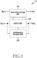
- FIG. 3 illustrates the functional configuration of an amplification circuit according to an embodiment of the disclosure.
- FIG. 3 further illustrates the configuration of the amplification circuit 112.
- the amplification circuit 112 includes a main amplifying unit 310, an output unit 320, and a common-mode feedback unit 330.
- the main amplifying unit 310 amplifies an input signal input through input terminals IN p and IN n .
- the amplified signal is provided to the output unit 320.
- the input signal may be a differential signal.
- the main amplifying unit 310 may include a part for improving broadband characteristics and a part for improving higher gain characteristics.
- the output unit 320 generates an output signal in response to the input signal amplified by the main amplifying unit 310.
- the output unit 320 has a structure folded with respect to the main amplifying unit 310 in order to secure the headroom of the output circuit.
- the common-mode feedback unit 330 is a feedback circuit installed in a bias part of the amplification circuit 112, and generates signals fed back from output terminals OUT p and OUT n .
- the common-mode feedback unit 330 may be used to stabilize a common mode of the amplification circuit 112.
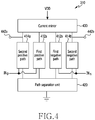
- FIG. 4 illustrates the configuration of a main amplifying unit of an amplification circuit according to an embodiment of the disclosure.
- FIG. 4 further illustrates the configuration of the main amplifying unit 310.
- the main amplifying unit 310 includes a first positive path 412a, a first negative path 412b, a second positive path 414a, a second negative path 414b, a path separation unit 420, and a current mirror 430.
- the first positive path 412a and the first negative path 412b generate first currents using input signals.
- the first positive path 412a generates a current corresponding to the voltage of a positive signal of a differential signal
- the first negative path 412b generates a current corresponding to the voltage of a negative signal of the differential signal.
- the first positive path 412a and the first negative path 412b may be collectively referred to as a first path.
- the second positive path 414a and the second negative path 414b generate second currents using the input signals.
- the second positive path 414a generates a current corresponding to the voltage of a positive signal of a differential signal
- the second negative path 414b generates a current corresponding to the voltage of a negative signal of the differential signal.
- the amount of second currents is greater than the amount of first currents.
- a ratio of the magnitude of the amount of first currents to the magnitude of the amount of second currents may be represented by 1: k.
- the first positive path 412a and the first negative path 412b may have relatively higher gain characteristics
- the second positive path 414a and the second negative path 414b may have relatively broadband characteristics.
- the second currents are provided to the output unit 320 through nodes 442a and 442b.
- the second positive path 414a and the second negative path 414b may be collectively referred to as a second path.
- the path separation unit 420 controls the first currents and the second currents.
- the path separation unit 420 includes a first grounding path for grounding the first positive path 412a and the first negative path 412b, and a second grounding path for grounding the second positive path 414a and the second negative path 414b.
- the first grounding path may include a circuit for controlling the first currents
- the second grounding path may include a circuit for controlling the second currents. Accordingly, the first currents and the second currents may be independently controlled by means of the path separation unit 420.
- the current mirror 430 generates third currents corresponding to first currents generated via the first positive path 412a and the first negative path 414a.
- the amount of the third currents is greater than the amount of the first currents.
- a ratio of the magnitude of the first currents to the magnitude of the third currents may be represented by 1:j.
- the third currents are provided to the output unit 320 via nodes 442a and 442b. Due to the gain of the current mirror 430, the overall gain of the amplification circuit 112 may be increased. In addition, due to the use of the current mirror 430, only one common-mode feedback circuit may be used and a parasitic pole frequency may be higher.
- FIG. 5 illustrates an implementation example of a main amplifying unit of an amplification circuit according to an embodiment of the disclosure.
- FIG. 5 further illustrates a detailed implementation example of a main amplifying unit 310.
- the main amplifying unit 310 includes a transistor 502a, a transistor 502b, a transistor 504a, a transistor 504b, a transistor 506a, a transistor 506b, a variable transistor 508a, a variable transistor 508b, a transistor 510a, a transistor 510b, a transistor 512a, and a transistor 512b.
- the transistors 502a, 502b, 506a, 506b, 508a, 508b are n-channel metal oxide semiconductor (NMOS) transistors
- the transistors 504a, 504b, 510a, 510b, 512a, 512b are p-channel metal oxide semiconductor (PMOS) transistors.
- p-type metal-oxide-semiconductor (PMOS) transistors may be replaced with NMOS transistors
- NMOS transistors may be replaced with PMOS transistors.
- the first positive path 412a includes the transistor 502a
- the first negative path 412b includes the transistor 502b.
- Input signals are applied to gates of the transistors 502a and 502b. Drains of the transistors 502a and 502b are connected to drains of the transistors 504a and 504b. Gates of the transistors 504a and 504b are connected to a bias vbcp.
- the second positive path 414a includes the transistor 506a
- the second negative path 414b includes the transistor 506b.
- Input signals are applied to gates of the transistors 506a and 506b.
- the ratio of the size of transistors 502a and 502b to the size of transistors 506a and 506b may be 1: k. Drains of the transistors 506a and 506b are connected to nodes 442a and 442b.
- the path separation unit 420 includes a variable transistor 508a and a variable transistor 508b.
- a bias vbn is applied to gates of the variable transistors 508a and 508b, and sources of the variable transistors 508a and 508b are grounded.
- a drain of the variable transistor 508a is connected to sources of the transistors 502a and 502b, and a drain of the variable transistor 508b is connected to sources of the transistors 506a and 506b.
- the ratio of the maximum size of the variable transistor 508a to that of the variable transistor 508b may be 1: k.
- the current mirror 430 includes a transistor 510a, a transistor 510b, a transistor 512a, and a transistor 512b.
- V DD is applied to sources of the transistors 510a, 510b, 512a, and 512b.
- Gates of transistors 510a and 510b are connected to gates of transistors 512a and 512b. That is, transistors 510a and 512b share a gate voltage, and transistors 510b and 512a share a gate voltage. Drains of the transistors 510a and 510b are connected to sources of the transistors 504a and 504b. Drains of transistors 512a and 512b are connected to nodes 422a and 422b.
- Each of the variable transistors 508a and 508b is variable to adjust the amount of corresponding current.
- each of the variable transistors 508a and 508b includes a plurality of NMOS transistors, and may have a structure in which some or all of the NMOS transistors are turned on depending on the intended amount of current.
- the gains g mn1 and g mn3 can be adjusted.
- the gain and bandwidth of the amplification circuit 112 can be adjusted.
- Parasitic capacitances 514a and 514b may be configured in gates of the transistors 510a and 510b.
- Equation 1 g mp1 denotes the gain of a current mirror corresponding to a first path
- g mp3 denotes the gain of a current mirror corresponding to a second path
- j denotes a ratio between gains of current mirrors
- g mn1 is a gain of the first path
- g mn3 denotes a gain of the second path
- k denotes a gain ratio between the first path and the second path.
- Equation 2 the overall gain of the amplification circuit 112 is defined by Equation 2 as follows.
- H s j + k g mn 1 r o 2 1 + sC o 1 j k + 1 g mp 1 1 + sC o 1 g mp 1 1 + sC o 2 g o 2
- H(s) denotes a transfer function of the amplification circuit 112
- j denotes a gain ratio of a current mirror
- k denotes a gain ratio between a first path and a second path
- g mn1 denotes a gain of the first path
- r o2 denotes a parasitic resistance at an output terminal
- C o1 denotes a parasitic capacitance 514b
- g mp1 denotes a gain of a current mirror corresponding to the first path
- C o2 denotes a parasitic capacitance at an output terminal
- g o2 denotes an inverse of r o2 .
- Equation 3 Each term included in the transfer function of Equation 2 may be defined by Equation 3.
- ⁇ z , LHP j k + 1 g mp 1 C o 1
- ⁇ p 1 g mp 1 C o 1
- ⁇ p 2 1 r o 2 C o 2
- Equation 3 ⁇ z, LHP denotes a frequency corresponding to a left-half- plane (LHP) zero, j denotes a gain ratio of a current mirror, k denotes a gain ratio between a first path and a second path, g mp1 denotes a gain of a current mirror corresponding to the first path, C o1 denotes a parasitic capacitance 514b, ⁇ p1 denotes a frequency at which a first pole occurs, ⁇ p2 denotes a frequency at which a second pole occurs, r o2 denotes parasitic resistance at an output terminal, and C o2 denotes parasitic capacitance at an output terminal.
- Equation 4 a low frequency gain may be defined by Equation 4 as follows.
- G DC j + k g mn 1 r o 2
- GBW gain bandwidth j + k g mn 1 r o 2 g mp 1 C o 1
- G DC denotes a low frequency gain
- j denotes a gain ratio of a current mirror
- k denotes a gain ratio between a first path and a second path
- g mn1 denotes a gain of the first path
- r o2 denotes parasitic resistance at an output terminal
- GBW denotes a gain bandwidth
- g mp1 denotes a gain of a current mirror corresponding to the first path
- C o1 denotes parasitic capacitance 514b.
- FIG. 6 illustrates an implementation example of an output unit of an amplification circuit according to an embodiment of the disclosure.
- FIG. 6 further illustrates an implementation example of an output unit 320.
- the output unit 320 includes a transistor 602a, a transistor 602b, a transistor 604a, a transistor 604b, a transistor 606a, a transistor 606b, a resistor 608a, and a resistor 608b.
- the transistors 602a and 602b are PMOS transistors, and the transistors 604a, 604b, 606a, and 606b are NMOS transistors.
- PMOS transistors may be replaced with NMOS transistors, and NMOS transistors may be replaced with PMOS transistors.
- a bias vbcp is applied to gates of the transistors 602a and 602b
- a bias vbcn is applied to gates of the transistors 604a and 604b
- a bias vcmfb is applied to gates of the transistors 606a and 606b.
- Sources of the transistors 602a and 602b are connected to nodes 442a and 442b
- drains of transistors 602a and 602b are connected to output terminals OUT n and OUT p . That is, the transistors 602a and 602b receive an input signal through sources and output an output signal through drains.
- One node of each of the resistors 608a and 608b is connected to a body terminal of a corresponding one of the transistors 602a and 602b, and V DD is applied to the other nodes of the resistors 608a and 608b.
- Drains of transistors 604a and 604b are respectively connected to output terminals OUT n and OUT p , and sources of transistors 604a and 604b are respectively connected to drains of transistors 606a and 606b. Sources of transistors 606a and 606b are grounded.
- transistors 504a, 504b, 602a, and 602b have cascode structure with transistors 510a, 510b, 512a, and 512b. Further, the transistors 504a, 504b, 602a, and 602b maintain the voltages of drains of the transistors 510a, 510b, 512a, and 512b included in a current mirror 430 constant, so as to maintain a current split ratio of the current mirror 430. In addition, the transistors 504a, 504b, 602a, 602b improve a gain by increasing the load impedance of the first positive path 412a, the first negative path 412b, the second positive path 414a, and the second negative path 414b.
- Resistors 608a and 608b are arranged between a V DD terminal and the transistors 602a and 602b, thereby functioning as high-impedance body biasing to the transistors 602a and 602b. Accordingly, the high frequency characteristics of the amplification circuit 112 can be improved. Transistors 604a and 604b and transistors 606a and 606b configure output impedance.
- Parasitic elements 610a and 610b may be configured at the output terminals OUT n and OUT p .
- the parasitic elements 610a and 610b may respectively be represented by a capacitor and a resistor connected in parallel.
- FIG. 7 illustrates an implementation example of a common-mode feedback unit of an amplification circuit according to an embodiment of the disclosure.
- FIG. 7 further illustrates an implementation example of the common-mode feedback unit 330.
- a common-mode feedback unit 330 includes transistors 702a, 702b, 704a, 704b, 706a, 706b, 708a, 708b, 710a, 710b, 712a, 712b, 714a, and 714b, and a resistor 716.
- the transistors 702a, 702b, 704a, 704b, 706a, 706b, 708a, 708b, 710a, 710b are PMOS transistors
- transistors 712a, 712b, 714a, 714b are NMOS transistors.
- PMOS transistors may be replaced with NMOS transistors
- NMOS transistors may be replaced with PMOS transistors.
- a bias vbp is applied to gates of the transistors 702a and 702b
- a bias vcm is applied to gates of the transistors 704a and 704b
- a bias vbcp2 is applied to gates of the transistors 708a and 708b
- a bias vbcp2 is applied to gates of the transistors 710a and 710b.
- the common-mode feedback unit 330 generates a bias vcmfb through the resistor 716 and applies a bias vcmfb to a main amplifier.
- V DD is applied to sources of transistors 702a and 702b.
- Sources of the transistors 704a and 704b are connected to drains of the transistors 702a and 702b, and drains of the transistors 704a and 704b are connected to sources of the transistors 708a and 708b.
- Sources of the transistors 706a and 706b are connected to the sources of transistors 704a and 704b, and gates of the transistors 706a and 706b are connected to output terminals OUT n and OUT p .
- Drains of the transistors 708a and 708b are interconnected and are also connected to the other node of the resistor 716.
- Sources of transistors 710a and 710b are connected to drains of transistors 706a and 706b. Drains of the transistors 712a and 712b are connected to the other node of the resistor 716, and sources of the transistors 712a and 712b are grounded.
- Gates of transistors 714a and 714b are connected to gates of transistors 712a and 712b, drains of transistors 714a and 714b are connected to drains of transistors 710a and 710b, and sources of transistors 714a and 714b are grounded.
- a capacitor 718 may be connected to one node of the resistor 716 for stabilization.
- capacitors 720a and 720b may be connected to the output terminals OUT n and OUT p via the vcmfb for stabilization.
- a computer-readable storage medium for storing one or more programs (software modules) may be provided.
- the one or more programs stored in the computer-readable storage medium may be configured for execution by one or more processors within the electronic device.
- the at least one program may include instructions that cause the electronic device to perform the methods according to various embodiments as defined by the appended claims and/or disclosed herein.
- the programs may be stored in nonvolatile memories including a random access memory and a flash memory, a read only memory (ROM), an electrically erasable programmable read only memory (EEPROM), a magnetic disc storage device, a compact disc-ROM (CD-ROM), digital versatile discs (DVDs), or other types of optical storage devices, or a magnetic cassette.
- ROM read only memory
- EEPROM electrically erasable programmable read only memory
- CD-ROM compact disc-ROM
- DVDs digital versatile discs
- any combination of some or all thereof may form a memory in which the program is stored.
- a plurality of such memories may be included in the electronic device.
- the programs may be stored in an attachable storage device which is accessible through communication networks such as the Internet, Intranet, local area network (LAN), wide area network (WAN), and storage area network (SAN), or a combination thereof.
- a storage device may access the electronic device via an external port.
- a separate storage device on the communication network may access a portable electronic device.
- multiple elements expressed in the description may be configured into a single element, or a single element in the description may be configured into multiple elements.
Landscapes
- Engineering & Computer Science (AREA)
- Power Engineering (AREA)
- Computer Networks & Wireless Communication (AREA)
- Signal Processing (AREA)
- Amplifiers (AREA)
Description
- The disclosure relates to an electronic circuit. More particularly, the disclosure relates to an apparatus including an electronic circuit for amplifying a signal.
- To meet the demand for wireless data traffic having increased since deployment of 4th generation (4G) communication systems, efforts have been made to develop an improved 5th generation (5G) or pre-5G communication system. Therefore, the 5G or pre-5G communication system is also called a 'Beyond 4G Network' or a 'Post Long-Term Evolution (LTE) System'.
- The 5G communication system is considered to be implemented in higher frequency (mmWave) bands, e.g., 60GHz bands, so as to accomplish higher data rates. To decrease propagation loss of the radio waves and increase the transmission distance, the beamforming, massive multiple-input multiple-output (MIMO), Full Dimensional MIMO (FD-MIMO), array antenna, an analog beam forming, large scale antenna techniques are discussed in 5G communication systems.
- In addition, in 5G communication systems, development for system network improvement is under way based on advanced small cells, cloud Radio Access Networks (RANs), ultra-dense networks, device-to-device (D2D) communication, wireless backhaul, moving network, cooperative communication, Coordinated Multi-Points (CoMP), reception-end interference cancellation and the like.
- In the 5G system, Hybrid frequency shift keying (FSK) and quadrature amplitude modulation (FQAM) and sliding window superposition coding (SWSC) as an advanced coding modulation (ACM), and filter bank multi carrier (FBMC), non-orthogonal multiple access (NOMA), and sparse code multiple access (SCMA) as an advanced access technology have been developed.
- Generally, an amplifier uses feedback to reduce a gain variation range under process, voltage, and temperature (PVT) conditions. If a feedback factor is referred to as "f' and an open loop gain is referred to as "A", the overall gain of an amplifier is approximated to A/ (1+f*A). Therefore, as the open-loop gain increases, the feedback gain approximates 1/f, and thus accurate feedback can be obtained. However, in a broadband amplifier, increasing the gain generally result in increasing bandwidth, and accordingly a phase margin is reduced, and thus stability is lowered. Therefore, in the design of a broadband amplifier, it is very difficult to secure stability while increasing the gain.
- The above information is presented as background information only to assist with an understanding of the disclosure. No determination has been made, and no assertion is made, as to whether any of the above might be applicable as prior art with regard to the disclosure.
-
US 20120019325A1 relates to a current-mode amplifier including an input stage, a feedback circuit and an output stage. - The invention is defined by the independent claims. The dependent claims define advantageous embodiments.
- While several embodiments and/or examples have been disclosed in this description, the subject-matter for which protection is sought is strictly and solely limited to those embodiments and/or examples encompassed by the scope of the appended claims. Embodiments and/or examples mentioned in the description that do not fall under the scope of the claims are useful for understanding the invention.
- The above and other aspects, features, and advantages of certain embodiments of the disclosure will be more apparent from the following description taken in conjunction with the accompanying drawings, in which:
-
FIG. 1 illustrates an apparatus including an amplification circuit according to an embodiment of the disclosure; -
FIG. 2 illustrates the conceptual configuration of an amplification circuit according to an embodiment of the disclosure; -
FIG. 3 illustrates the functional configuration of an amplification circuit according to an embodiment of the disclosure; -
FIG. 4 illustrates a configuration of a main amplifying unit of an amplification circuit according to an embodiment of the disclosure; -
FIG. 5 illustrates an implementation example of a main amplifying unit of an amplification circuit according to an embodiment of the disclosure; -
FIG. 6 illustrates an implementation example of an output unit of an amplification circuit according to an embodiment of the disclosure; and -
FIG. 7 illustrates an implementation example of a common-mode feedback unit of an amplification circuit according to an embodiment of the disclosure. - Throughout the drawings, it should be noted that like reference numbers are used to depict the same or similar elements, features, and structures.
- The following description with reference to the accompanying drawings is provided to assist in a comprehensive understanding of various embodiments of the disclosure as defined by the claims and their equivalents. It includes various specific details to assist in that understanding but these are to be regarded as merely exemplary. Accordingly, those of ordinary skill in the art will recognize that various changes and modifications of the various embodiments described herein can be made without departing from the scope and spirit of the disclosure. In addition, descriptions of well-known functions and constructions may be omitted for clarity and conciseness.
- The terms and words used in the following description and claims are not limited to the bibliographical meanings, but, are merely used by the inventor to enable a clear and consistent understanding of the disclosure. Accordingly, it should be apparent to those skilled in the art that the following description of various embodiments of the disclosure is provided for illustration purpose only and not for the purpose of limiting the disclosure as defined by the appended claims and their equivalents.
- It is to be understood that the singular forms "a," "an," and "the" include plural referents unless the context clearly dictates otherwise. Thus, for example, reference to "a component surface" includes reference to one or more of such surfaces.
- Hereinafter, the disclosure relates to an apparatus including an electronic circuit for amplifying a signal. Specifically, a circuit structure of an amplifier having a higher gain and broadband characteristics will be described.
- Terms referring to signals, terms referring to materials, terms referring to structures, terms referring to elements of circuits, and the like, which will be used in the following description, are used for convenience of explanation. Accordingly, the disclosure is not limited to the following terms, and other terms having the same technical meanings may be used.
-
FIG. 1 illustrates an apparatus including an amplification circuit according to an embodiment of the disclosure. - Referring to
FIG. 1 , an apparatus includes a communication unit 110 (e.g., a transceiver including a transmission unit) and a controller 120 (e.g., at least one processor). - The
communication unit 110 performs functions for transmitting or receiving a signal. For example, thecommunication unit 110 may perform conversion between a bit string and a baseband signal, conversion between an analog signal and a digital signal, conversion between a baseband signal and an intermediate frequency (IF)/ radio frequency (RF) signal, and the like. According to various embodiments, thecommunication unit 110 includes anamplification circuit 112 configured to amplify a transmission signal or a reception signal. Theamplification circuit 112 may amplify at least one of a baseband signal, an intermediate frequency band signal, and an RF signal. - The
controller 120 controls the overall operation of the apparatus. Thecontroller 120 may provide transmission data to thecommunication unit 110 and process reception data provided from thecommunication unit 110. In addition, thecontroller 120 may determine and control the state of an element (e.g., the amplification circuit 112) included in thecommunication unit 110. Thecontroller 120 may generate and output a control signal for controlling thecommunication unit 110. To this end, thecontroller 120 may include at least one of a processor, a microprocessor, a microcontroller, a memory, and a control signal generation circuit. -
FIG. 2 illustrates the conceptual configuration of an amplification circuit according to an embodiment of the disclosure. - Referring to
FIG. 2 , theamplification circuit 112 includes afirst element 202 configured to provide a gain gmn1 and asecond element 204 configured to provide a gain gmn3. In addition, theamplification circuit 112 includes athird element 206 configured to increase a gain by j times. According to an embodiment, thefirst element 202 may have relatively higher gain characteristics, and thesecond element 204 may have relatively broadband characteristics. -
FIG. 3 illustrates the functional configuration of an amplification circuit according to an embodiment of the disclosure.FIG. 3 further illustrates the configuration of theamplification circuit 112. - Referring to
FIG. 3 , theamplification circuit 112 includes amain amplifying unit 310, anoutput unit 320, and a common-mode feedback unit 330. - The
main amplifying unit 310 amplifies an input signal input through input terminals INp and INn. The amplified signal is provided to theoutput unit 320. Here, the input signal may be a differential signal. According to various embodiments, themain amplifying unit 310 may include a part for improving broadband characteristics and a part for improving higher gain characteristics. - The
output unit 320 generates an output signal in response to the input signal amplified by themain amplifying unit 310. Theoutput unit 320 has a structure folded with respect to themain amplifying unit 310 in order to secure the headroom of the output circuit. - The common-
mode feedback unit 330 is a feedback circuit installed in a bias part of theamplification circuit 112, and generates signals fed back from output terminals OUTp and OUTn. The common-mode feedback unit 330 may be used to stabilize a common mode of theamplification circuit 112. -
FIG. 4 illustrates the configuration of a main amplifying unit of an amplification circuit according to an embodiment of the disclosure.FIG. 4 further illustrates the configuration of themain amplifying unit 310. - Referring to
FIG. 4 , themain amplifying unit 310 includes a firstpositive path 412a, a firstnegative path 412b, a secondpositive path 414a, a secondnegative path 414b, apath separation unit 420, and acurrent mirror 430. - The first
positive path 412a and the firstnegative path 412b generate first currents using input signals. The firstpositive path 412a generates a current corresponding to the voltage of a positive signal of a differential signal, and the firstnegative path 412b generates a current corresponding to the voltage of a negative signal of the differential signal. The firstpositive path 412a and the firstnegative path 412b may be collectively referred to as a first path. - The second
positive path 414a and the secondnegative path 414b generate second currents using the input signals. The secondpositive path 414a generates a current corresponding to the voltage of a positive signal of a differential signal, and the secondnegative path 414b generates a current corresponding to the voltage of a negative signal of the differential signal. Here, the amount of second currents is greater than the amount of first currents. For example, a ratio of the magnitude of the amount of first currents to the magnitude of the amount of second currents may be represented by 1: k. Accordingly, the firstpositive path 412a and the firstnegative path 412b may have relatively higher gain characteristics, and the secondpositive path 414a and the secondnegative path 414b may have relatively broadband characteristics. The second currents are provided to theoutput unit 320 throughnodes positive path 414a and the secondnegative path 414b may be collectively referred to as a second path. - The
path separation unit 420 controls the first currents and the second currents. Thepath separation unit 420 includes a first grounding path for grounding the firstpositive path 412a and the firstnegative path 412b, and a second grounding path for grounding the secondpositive path 414a and the secondnegative path 414b. The first grounding path may include a circuit for controlling the first currents, and the second grounding path may include a circuit for controlling the second currents. Accordingly, the first currents and the second currents may be independently controlled by means of thepath separation unit 420. - The
current mirror 430 generates third currents corresponding to first currents generated via the firstpositive path 412a and the firstnegative path 414a. Here, the amount of the third currents is greater than the amount of the first currents. For example, a ratio of the magnitude of the first currents to the magnitude of the third currents may be represented by 1:j. The third currents are provided to theoutput unit 320 vianodes current mirror 430, the overall gain of theamplification circuit 112 may be increased. In addition, due to the use of thecurrent mirror 430, only one common-mode feedback circuit may be used and a parasitic pole frequency may be higher. -
FIG. 5 illustrates an implementation example of a main amplifying unit of an amplification circuit according to an embodiment of the disclosure.FIG. 5 further illustrates a detailed implementation example of amain amplifying unit 310. - Referring to
FIG. 5 , themain amplifying unit 310 includes atransistor 502a, atransistor 502b, atransistor 504a, atransistor 504b, atransistor 506a, atransistor 506b, avariable transistor 508a, avariable transistor 508b, atransistor 510a, atransistor 510b, atransistor 512a, and atransistor 512b. Thetransistors transistors - The first
positive path 412a includes thetransistor 502a, and the firstnegative path 412b includes thetransistor 502b. Input signals are applied to gates of thetransistors transistors transistors transistors - The second
positive path 414a includes thetransistor 506a, and the secondnegative path 414b includes thetransistor 506b. Input signals are applied to gates of thetransistors transistors transistors transistors transistors nodes - The
path separation unit 420 includes avariable transistor 508a and avariable transistor 508b. A bias vbn is applied to gates of thevariable transistors variable transistors variable transistor 508a is connected to sources of thetransistors variable transistor 508b is connected to sources of thetransistors variable transistor 508a to that of thevariable transistor 508b may be 1: k. - The
current mirror 430 includes atransistor 510a, atransistor 510b, atransistor 512a, and atransistor 512b. VDD is applied to sources of thetransistors transistors transistors transistors transistors transistors transistors transistors - Each of the
variable transistors variable transistors variable transistors variable transistors amplification circuit 112 can be adjusted. -
Parasitic capacitances transistors - The characteristics of the circuit illustrated in
FIG. 5 will be described with reference to the following equations.
- In
Equation 1, gmp1 denotes the gain of a current mirror corresponding to a first path, gmp3 denotes the gain of a current mirror corresponding to a second path, j denotes a ratio between gains of current mirrors, gmn1 is a gain of the first path, gmn3 denotes a gain of the second path, and k denotes a gain ratio between the first path and the second path. - Here, the overall gain of the
amplification circuit 112 is defined by Equation 2 as follows.
- In Equation 2, H(s) denotes a transfer function of the
amplification circuit 112, j denotes a gain ratio of a current mirror, k denotes a gain ratio between a first path and a second path, gmn1 denotes a gain of the first path, ro2 denotes a parasitic resistance at an output terminal, Co1 denotes aparasitic capacitance 514b, gmp1 denotes a gain of a current mirror corresponding to the first path, Co2 denotes a parasitic capacitance at an output terminal, and go2 denotes an inverse of ro2. - Each term included in the transfer function of Equation 2 may be defined by Equation 3.

- In Equation 3, ωz, LHP denotes a frequency corresponding to a left-half- plane (LHP) zero, j denotes a gain ratio of a current mirror, k denotes a gain ratio between a first path and a second path, gmp1 denotes a gain of a current mirror corresponding to the first path, Co1 denotes a
parasitic capacitance 514b, ωp1 denotes a frequency at which a first pole occurs, ωp2 denotes a frequency at which a second pole occurs, ro2 denotes parasitic resistance at an output terminal, and Co2 denotes parasitic capacitance at an output terminal. - Here, if ωz, LHP cancels ωp2, a low frequency gain may be defined by Equation 4 as follows.

- In Equation 4, GDC denotes a low frequency gain, j denotes a gain ratio of a current mirror, k denotes a gain ratio between a first path and a second path, gmn1 denotes a gain of the first path, ro2 denotes parasitic resistance at an output terminal, GBW denotes a gain bandwidth, gmp1 denotes a gain of a current mirror corresponding to the first path, and Co1 denotes
parasitic capacitance 514b. -
FIG. 6 illustrates an implementation example of an output unit of an amplification circuit according to an embodiment of the disclosure.FIG. 6 further illustrates an implementation example of anoutput unit 320. - Referring to
FIG. 6 , theoutput unit 320 includes atransistor 602a, atransistor 602b, atransistor 604a, atransistor 604b, atransistor 606a, atransistor 606b, aresistor 608a, and aresistor 608b. Thetransistors transistors - A bias vbcp is applied to gates of the
transistors transistors transistors transistors nodes transistors transistors resistors transistors resistors transistors transistors transistors transistors - Referring to
FIG. 5 and6 ,transistors transistors transistors transistors current mirror 430 constant, so as to maintain a current split ratio of thecurrent mirror 430. In addition, thetransistors positive path 412a, the firstnegative path 412b, the secondpositive path 414a, and the secondnegative path 414b. -
Resistors transistors transistors amplification circuit 112 can be improved.Transistors transistors -
Parasitic elements parasitic elements -
FIG. 7 illustrates an implementation example of a common-mode feedback unit of an amplification circuit according to an embodiment of the disclosure.FIG. 7 further illustrates an implementation example of the common-mode feedback unit 330. - Referring to
FIG. 7 , a common-mode feedback unit 330 includestransistors resistor 716. Thetransistors transistors - A bias vbp is applied to gates of the
transistors transistors transistors transistors 710a and 710b. The common-mode feedback unit 330 generates a bias vcmfb through theresistor 716 and applies a bias vcmfb to a main amplifier. VDD is applied to sources oftransistors transistors transistors transistors transistors transistors transistors transistors - Drains of the
transistors resistor 716. Sources oftransistors 710a and 710b are connected to drains oftransistors transistors resistor 716, and sources of thetransistors transistors transistors transistors transistors 710a and 710b, and sources oftransistors - A capacitor 718 may be connected to one node of the
resistor 716 for stabilization. In addition,capacitors 720a and 720b may be connected to the output terminals OUTn and OUTp via the vcmfb for stabilization. - Methods according to embodiments stated in claims and/or specifications of the disclosure may be implemented in hardware, software, or a combination of hardware and software.
- When the methods are implemented by software, a computer-readable storage medium for storing one or more programs (software modules) may be provided. The one or more programs stored in the computer-readable storage medium may be configured for execution by one or more processors within the electronic device. The at least one program may include instructions that cause the electronic device to perform the methods according to various embodiments as defined by the appended claims and/or disclosed herein.
- The programs (software modules or software) may be stored in nonvolatile memories including a random access memory and a flash memory, a read only memory (ROM), an electrically erasable programmable read only memory (EEPROM), a magnetic disc storage device, a compact disc-ROM (CD-ROM), digital versatile discs (DVDs), or other types of optical storage devices, or a magnetic cassette. Alternatively, any combination of some or all thereof may form a memory in which the program is stored. Further, a plurality of such memories may be included in the electronic device.
- In addition, the programs may be stored in an attachable storage device which is accessible through communication networks such as the Internet, Intranet, local area network (LAN), wide area network (WAN), and storage area network (SAN), or a combination thereof. Such a storage device may access the electronic device via an external port. Further, a separate storage device on the communication network may access a portable electronic device.
- Further, multiple elements expressed in the description may be configured into a single element, or a single element in the description may be configured into multiple elements.
Claims (13)
- An apparatus comprising an electronic circuit, the apparatus comprising:a transceiver (110) including an amplification circuit (112); andat least one processor (120) coupled to the transceiver,wherein the amplification circuit (112) comprises:a main amplifying circuit (310) configured to amplify an input signal input through input terminals, comprising:a first path (412a, 412b) configured to generate a first current corresponding to a voltage of an input signal,a second path (414a, 414b) configured to generate a second current corresponding to the voltage of the input signal, wherein an amount of the second current is greater than an amount of the first current,a separation unit (420) configured to control each of the first current and the second current, anda current mirror (430) configured to generate a third current corresponding to the first current, wherein an amount of the third current is greater than the amount of the first current;an output circuit (320) comprising a folding unit to generate an output signal on a basis of the second current and the third current; anda common-mode feedback circuit (330) configured to generate a feedback signal from the output signal,wherein the output circuit is in communication with the main amplifying circuit and the common-mode feedback circuit.
- The apparatus of claim 1, wherein the second path includes a transistor that is larger than transistors included in the first path.
- The apparatus of claim 1, wherein the input signal is input to gates of transistors included in the first path and the second path.
- The apparatus of claim 1, further comprising:
transistors connected, in a cascode structure, to transistors included in the first path, between the first path and the current mirror. - The apparatus of claim 1, wherein the separation unit comprises:a first variable transistor connected to the first path, anda second variable transistor connected to the second path.
- The apparatus of claim 5,
wherein a gate of the first variable transistor and a gate of the second variable transistor are connected to the same bias,
wherein a drain of the first variable transistor is connected to sources of transistors included in the first path,
wherein a drain of the second variable transistor is connected to sources of transistors included in the second path, and
wherein sources of the first variable transistor and the second variable transistor are grounded. - The apparatus of claim 1,
wherein the current mirror comprises:first transistors having the same gain as that of the first path, andsecond transistors having a higher gain than that of the first path, and wherein the first transistors and the second transistors share a gate voltage. - The apparatus of claim 1, wherein the folding unit comprises transistors configured to:receive the second current and the third current through sources; andoutput the output signal through drains.
- The apparatus of claim 8, wherein the folding unit comprises resistors connected to body terminals of the transistors.
- The apparatus of claim 1, wherein the main amplifying circuit further comprises:a first part to improve broadband characteristics, anda second part to improve higher gain characteristics.
- The apparatus of claim 1, wherein the common-mode feedback circuit comprises a feedback circuit installed in a bias part of the amplification circuit.
- The apparatus of claim 1, wherein the output circuit comprises a structure folded with respect to the main amplifying circuit to secure headroom of the output circuit.
- The apparatus of claim 1,
wherein the common-mode feedback circuit comprises a feedback circuit installed in a bias part of the amplification circuit,
wherein the common-mode feedback circuit is configured to: generate a fed-back signal from the output signal, and stabilize a common mode of the amplification circuit.
Applications Claiming Priority (1)
| Application Number | Priority Date | Filing Date | Title |
|---|---|---|---|
| KR1020190009610A KR102743743B1 (en) | 2019-01-25 | 2019-01-25 | Apparatus including electronic circuit for amplifying signal |
Publications (2)
| Publication Number | Publication Date |
|---|---|
| EP3694111A1 EP3694111A1 (en) | 2020-08-12 |
| EP3694111B1 true EP3694111B1 (en) | 2021-06-23 |
Family
ID=69190651
Family Applications (1)
| Application Number | Title | Priority Date | Filing Date |
|---|---|---|---|
| EP20153320.5A Active EP3694111B1 (en) | 2019-01-25 | 2020-01-23 | Apparatus including electronic circuit for amplifying signal |
Country Status (4)
| Country | Link |
|---|---|
| US (1) | US11342893B2 (en) |
| EP (1) | EP3694111B1 (en) |
| KR (1) | KR102743743B1 (en) |
| CN (1) | CN111565029B (en) |
Families Citing this family (1)
| Publication number | Priority date | Publication date | Assignee | Title |
|---|---|---|---|---|
| KR102835087B1 (en) * | 2023-05-15 | 2025-07-16 | 조선대학교 산학협력단 | Variable gain amplifier |
Family Cites Families (13)
| Publication number | Priority date | Publication date | Assignee | Title |
|---|---|---|---|---|
| US5581212A (en) | 1993-10-18 | 1996-12-03 | Industrial Technology Research Institute | Fully differential CMOS transconductance-transimpedance wide-band amplifier |
| US7505750B2 (en) * | 2005-07-01 | 2009-03-17 | Broadcom Corporation | Mixer transconductance in RF transceiver |
| US7409198B2 (en) * | 2005-08-30 | 2008-08-05 | Freescale Semiconductor, Inc. | Wideband variable gain amplifier in an ultra wideband receiver |
| US8143957B2 (en) | 2006-01-11 | 2012-03-27 | Qualcomm, Incorporated | Current-mode gain-splitting dual-path VCO |
| TWI462496B (en) * | 2007-10-03 | 2014-11-21 | Airoha Tech Corp | The biasing circuit of the wireless transceiver |
| ATE515104T1 (en) * | 2008-07-25 | 2011-07-15 | St Ericsson Belgium Nv | MIXER CELL WITH A DYNAMIC CURRENT DRAIN CIRCUIT |
| US7906994B2 (en) * | 2009-02-24 | 2011-03-15 | Standard Microsystems Corporation | Fast common mode feedback control for differential driver |
| GB2477572B (en) | 2010-02-09 | 2012-01-04 | Toshiba Res Europ Ltd | High power wideband amplifier and method |
| TWI413361B (en) * | 2010-07-20 | 2013-10-21 | Ind Tech Res Inst | Current-mode amplifier |
| US9559646B2 (en) * | 2014-09-10 | 2017-01-31 | Samsung Electronics Co., Ltd | Apparatus and method for dynamically biased baseband current amplifier |
| US10079582B2 (en) | 2015-12-18 | 2018-09-18 | Qualcomm Incorporated | Wideband amplifier circuits and methods |
| KR20170075892A (en) * | 2015-12-23 | 2017-07-04 | 에스케이하이닉스 주식회사 | Differential amplifier circuit, voltage regulator and semiconductor memory device including the same |
| CN107947747A (en) * | 2017-11-21 | 2018-04-20 | 中国地质大学(北京) | Folded common source and common grid amplifier and analog circuit |
-
2019
- 2019-01-25 KR KR1020190009610A patent/KR102743743B1/en active Active
-
2020
- 2020-01-23 US US16/750,552 patent/US11342893B2/en active Active
- 2020-01-23 CN CN202010076383.6A patent/CN111565029B/en active Active
- 2020-01-23 EP EP20153320.5A patent/EP3694111B1/en active Active
Also Published As
| Publication number | Publication date |
|---|---|
| CN111565029A (en) | 2020-08-21 |
| US20200244237A1 (en) | 2020-07-30 |
| US11342893B2 (en) | 2022-05-24 |
| KR20200092558A (en) | 2020-08-04 |
| EP3694111A1 (en) | 2020-08-12 |
| KR102743743B1 (en) | 2024-12-17 |
| CN111565029B (en) | 2026-02-13 |
Similar Documents
| Publication | Publication Date | Title |
|---|---|---|
| US10797662B2 (en) | Amplifying circuit including miller compensation circuit | |
| US10019023B2 (en) | Low-dropout linear regulator with super transconductance structure | |
| EP0663719B1 (en) | Analog filter circuit and semiconductor integrated circuit device using the same | |
| US7009452B2 (en) | Method and apparatus for increasing the linearity and bandwidth of an amplifier | |
| US10078342B2 (en) | Low dropout voltage regulator with variable load compensation | |
| US12146902B2 (en) | Power detector | |
| US9998077B2 (en) | Amplifier with nonlinearity compensation | |
| US8442464B2 (en) | Low noise amplifier and mixer | |
| JP2015128236A (en) | Differential signal drive circuit | |
| US11693441B2 (en) | Dual loop voltage regulator utilizing gain and phase shaping | |
| CN114123984B (en) | A power detection circuit and integrated chip | |
| US10348260B2 (en) | Amplifier circuit and filter | |
| EP3694111A1 (en) | Apparatus including electronic circuit for amplifying signal | |
| US20080218267A1 (en) | Amplifier with level shifting feedback network | |
| US7154335B2 (en) | Variable gain amplifier with direct current offset correction | |
| US6995615B2 (en) | Current-mode preamplifiers | |
| US6137832A (en) | Adaptive equalizer | |
| Yang et al. | A wideband transimpedance amplifier with tee network topology | |
| CN113917968A (en) | High-power linear voltage stabilizer | |
| CN120179008B (en) | LDO loop compensation circuit with wide output capacitance range | |
| US12620936B2 (en) | Mixer with reduced local oscillator (LO) leakage | |
| US20230163725A1 (en) | Semiconductor device and communication device comprising the same | |
| Sama et al. | Miller’s Compensation Techniques for a High Gain, High BW OP-AMP at 65 nm Technology | |
| KR102095869B1 (en) | An active quadrature signal generator with broadband quadrature characteristic | |
| US7586342B2 (en) | Programmable amplitude compensation circuit |
Legal Events
| Date | Code | Title | Description |
|---|---|---|---|
| PUAI | Public reference made under article 153(3) epc to a published international application that has entered the european phase |
Free format text: ORIGINAL CODE: 0009012 |
|
| STAA | Information on the status of an ep patent application or granted ep patent |
Free format text: STATUS: THE APPLICATION HAS BEEN PUBLISHED |
|
| AK | Designated contracting states |
Kind code of ref document: A1 Designated state(s): AL AT BE BG CH CY CZ DE DK EE ES FI FR GB GR HR HU IE IS IT LI LT LU LV MC MK MT NL NO PL PT RO RS SE SI SK SM TR |
|
| AX | Request for extension of the european patent |
Extension state: BA ME |
|
| STAA | Information on the status of an ep patent application or granted ep patent |
Free format text: STATUS: REQUEST FOR EXAMINATION WAS MADE |
|
| 17P | Request for examination filed |
Effective date: 20201125 |
|
| RBV | Designated contracting states (corrected) |
Designated state(s): AL AT BE BG CH CY CZ DE DK EE ES FI FR GB GR HR HU IE IS IT LI LT LU LV MC MK MT NL NO PL PT RO RS SE SI SK SM TR |
|
| GRAP | Despatch of communication of intention to grant a patent |
Free format text: ORIGINAL CODE: EPIDOSNIGR1 |
|
| STAA | Information on the status of an ep patent application or granted ep patent |
Free format text: STATUS: GRANT OF PATENT IS INTENDED |
|
| RIC1 | Information provided on ipc code assigned before grant |
Ipc: H04B 1/04 20060101AFI20210119BHEP Ipc: H03F 3/193 20060101ALI20210119BHEP Ipc: H03F 3/45 20060101ALI20210119BHEP |
|
| INTG | Intention to grant announced |
Effective date: 20210212 |
|
| GRAS | Grant fee paid |
Free format text: ORIGINAL CODE: EPIDOSNIGR3 |
|
| GRAA | (expected) grant |
Free format text: ORIGINAL CODE: 0009210 |
|
| STAA | Information on the status of an ep patent application or granted ep patent |
Free format text: STATUS: THE PATENT HAS BEEN GRANTED |
|
| AK | Designated contracting states |
Kind code of ref document: B1 Designated state(s): AL AT BE BG CH CY CZ DE DK EE ES FI FR GB GR HR HU IE IS IT LI LT LU LV MC MK MT NL NO PL PT RO RS SE SI SK SM TR |
|
| REG | Reference to a national code |
Ref country code: GB Ref legal event code: FG4D |
|
| REG | Reference to a national code |
Ref country code: CH Ref legal event code: EP |
|
| REG | Reference to a national code |
Ref country code: DE Ref legal event code: R096 Ref document number: 602020000173 Country of ref document: DE Ref country code: AT Ref legal event code: REF Ref document number: 1405206 Country of ref document: AT Kind code of ref document: T Effective date: 20210715 |
|
| REG | Reference to a national code |
Ref country code: IE Ref legal event code: FG4D |
|
| REG | Reference to a national code |
Ref country code: LT Ref legal event code: MG9D |
|
| PG25 | Lapsed in a contracting state [announced via postgrant information from national office to epo] |
Ref country code: LT Free format text: LAPSE BECAUSE OF FAILURE TO SUBMIT A TRANSLATION OF THE DESCRIPTION OR TO PAY THE FEE WITHIN THE PRESCRIBED TIME-LIMIT Effective date: 20210623 Ref country code: HR Free format text: LAPSE BECAUSE OF FAILURE TO SUBMIT A TRANSLATION OF THE DESCRIPTION OR TO PAY THE FEE WITHIN THE PRESCRIBED TIME-LIMIT Effective date: 20210623 Ref country code: FI Free format text: LAPSE BECAUSE OF FAILURE TO SUBMIT A TRANSLATION OF THE DESCRIPTION OR TO PAY THE FEE WITHIN THE PRESCRIBED TIME-LIMIT Effective date: 20210623 Ref country code: BG Free format text: LAPSE BECAUSE OF FAILURE TO SUBMIT A TRANSLATION OF THE DESCRIPTION OR TO PAY THE FEE WITHIN THE PRESCRIBED TIME-LIMIT Effective date: 20210923 |
|
| REG | Reference to a national code |
Ref country code: AT Ref legal event code: MK05 Ref document number: 1405206 Country of ref document: AT Kind code of ref document: T Effective date: 20210623 |
|
| PG25 | Lapsed in a contracting state [announced via postgrant information from national office to epo] |
Ref country code: GR Free format text: LAPSE BECAUSE OF FAILURE TO SUBMIT A TRANSLATION OF THE DESCRIPTION OR TO PAY THE FEE WITHIN THE PRESCRIBED TIME-LIMIT Effective date: 20210924 Ref country code: LV Free format text: LAPSE BECAUSE OF FAILURE TO SUBMIT A TRANSLATION OF THE DESCRIPTION OR TO PAY THE FEE WITHIN THE PRESCRIBED TIME-LIMIT Effective date: 20210623 Ref country code: NO Free format text: LAPSE BECAUSE OF FAILURE TO SUBMIT A TRANSLATION OF THE DESCRIPTION OR TO PAY THE FEE WITHIN THE PRESCRIBED TIME-LIMIT Effective date: 20210923 Ref country code: RS Free format text: LAPSE BECAUSE OF FAILURE TO SUBMIT A TRANSLATION OF THE DESCRIPTION OR TO PAY THE FEE WITHIN THE PRESCRIBED TIME-LIMIT Effective date: 20210623 Ref country code: SE Free format text: LAPSE BECAUSE OF FAILURE TO SUBMIT A TRANSLATION OF THE DESCRIPTION OR TO PAY THE FEE WITHIN THE PRESCRIBED TIME-LIMIT Effective date: 20210623 |
|
| REG | Reference to a national code |
Ref country code: NL Ref legal event code: MP Effective date: 20210623 |
|
| PG25 | Lapsed in a contracting state [announced via postgrant information from national office to epo] |
Ref country code: ES Free format text: LAPSE BECAUSE OF FAILURE TO SUBMIT A TRANSLATION OF THE DESCRIPTION OR TO PAY THE FEE WITHIN THE PRESCRIBED TIME-LIMIT Effective date: 20210623 Ref country code: EE Free format text: LAPSE BECAUSE OF FAILURE TO SUBMIT A TRANSLATION OF THE DESCRIPTION OR TO PAY THE FEE WITHIN THE PRESCRIBED TIME-LIMIT Effective date: 20210623 Ref country code: SK Free format text: LAPSE BECAUSE OF FAILURE TO SUBMIT A TRANSLATION OF THE DESCRIPTION OR TO PAY THE FEE WITHIN THE PRESCRIBED TIME-LIMIT Effective date: 20210623 Ref country code: CZ Free format text: LAPSE BECAUSE OF FAILURE TO SUBMIT A TRANSLATION OF THE DESCRIPTION OR TO PAY THE FEE WITHIN THE PRESCRIBED TIME-LIMIT Effective date: 20210623 Ref country code: AT Free format text: LAPSE BECAUSE OF FAILURE TO SUBMIT A TRANSLATION OF THE DESCRIPTION OR TO PAY THE FEE WITHIN THE PRESCRIBED TIME-LIMIT Effective date: 20210623 Ref country code: SM Free format text: LAPSE BECAUSE OF FAILURE TO SUBMIT A TRANSLATION OF THE DESCRIPTION OR TO PAY THE FEE WITHIN THE PRESCRIBED TIME-LIMIT Effective date: 20210623 Ref country code: RO Free format text: LAPSE BECAUSE OF FAILURE TO SUBMIT A TRANSLATION OF THE DESCRIPTION OR TO PAY THE FEE WITHIN THE PRESCRIBED TIME-LIMIT Effective date: 20210623 Ref country code: PT Free format text: LAPSE BECAUSE OF FAILURE TO SUBMIT A TRANSLATION OF THE DESCRIPTION OR TO PAY THE FEE WITHIN THE PRESCRIBED TIME-LIMIT Effective date: 20211025 Ref country code: NL Free format text: LAPSE BECAUSE OF FAILURE TO SUBMIT A TRANSLATION OF THE DESCRIPTION OR TO PAY THE FEE WITHIN THE PRESCRIBED TIME-LIMIT Effective date: 20210623 |
|
| PG25 | Lapsed in a contracting state [announced via postgrant information from national office to epo] |
Ref country code: PL Free format text: LAPSE BECAUSE OF FAILURE TO SUBMIT A TRANSLATION OF THE DESCRIPTION OR TO PAY THE FEE WITHIN THE PRESCRIBED TIME-LIMIT Effective date: 20210623 |
|
| REG | Reference to a national code |
Ref country code: DE Ref legal event code: R097 Ref document number: 602020000173 Country of ref document: DE |
|
| PG25 | Lapsed in a contracting state [announced via postgrant information from national office to epo] |
Ref country code: DK Free format text: LAPSE BECAUSE OF FAILURE TO SUBMIT A TRANSLATION OF THE DESCRIPTION OR TO PAY THE FEE WITHIN THE PRESCRIBED TIME-LIMIT Effective date: 20210623 |
|
| PLBE | No opposition filed within time limit |
Free format text: ORIGINAL CODE: 0009261 |
|
| STAA | Information on the status of an ep patent application or granted ep patent |
Free format text: STATUS: NO OPPOSITION FILED WITHIN TIME LIMIT |
|
| 26N | No opposition filed |
Effective date: 20220324 |
|
| PG25 | Lapsed in a contracting state [announced via postgrant information from national office to epo] |
Ref country code: AL Free format text: LAPSE BECAUSE OF FAILURE TO SUBMIT A TRANSLATION OF THE DESCRIPTION OR TO PAY THE FEE WITHIN THE PRESCRIBED TIME-LIMIT Effective date: 20210623 |
|
| PG25 | Lapsed in a contracting state [announced via postgrant information from national office to epo] |
Ref country code: IT Free format text: LAPSE BECAUSE OF FAILURE TO SUBMIT A TRANSLATION OF THE DESCRIPTION OR TO PAY THE FEE WITHIN THE PRESCRIBED TIME-LIMIT Effective date: 20210623 |
|
| PG25 | Lapsed in a contracting state [announced via postgrant information from national office to epo] |
Ref country code: MC Free format text: LAPSE BECAUSE OF FAILURE TO SUBMIT A TRANSLATION OF THE DESCRIPTION OR TO PAY THE FEE WITHIN THE PRESCRIBED TIME-LIMIT Effective date: 20210623 |
|
| REG | Reference to a national code |
Ref country code: BE Ref legal event code: MM Effective date: 20220131 |
|
| PG25 | Lapsed in a contracting state [announced via postgrant information from national office to epo] |
Ref country code: LU Free format text: LAPSE BECAUSE OF NON-PAYMENT OF DUE FEES Effective date: 20220123 |
|
| PG25 | Lapsed in a contracting state [announced via postgrant information from national office to epo] |
Ref country code: FR Free format text: LAPSE BECAUSE OF NON-PAYMENT OF DUE FEES Effective date: 20220131 Ref country code: BE Free format text: LAPSE BECAUSE OF NON-PAYMENT OF DUE FEES Effective date: 20220131 |
|
| PG25 | Lapsed in a contracting state [announced via postgrant information from national office to epo] |
Ref country code: IE Free format text: LAPSE BECAUSE OF NON-PAYMENT OF DUE FEES Effective date: 20220123 |
|
| REG | Reference to a national code |
Ref country code: CH Ref legal event code: PL |
|
| PG25 | Lapsed in a contracting state [announced via postgrant information from national office to epo] |
Ref country code: CH Free format text: LAPSE BECAUSE OF NON-PAYMENT OF DUE FEES Effective date: 20230131 Ref country code: LI Free format text: LAPSE BECAUSE OF NON-PAYMENT OF DUE FEES Effective date: 20230131 |
|
| PG25 | Lapsed in a contracting state [announced via postgrant information from national office to epo] |
Ref country code: MK Free format text: LAPSE BECAUSE OF FAILURE TO SUBMIT A TRANSLATION OF THE DESCRIPTION OR TO PAY THE FEE WITHIN THE PRESCRIBED TIME-LIMIT Effective date: 20210623 Ref country code: CY Free format text: LAPSE BECAUSE OF FAILURE TO SUBMIT A TRANSLATION OF THE DESCRIPTION OR TO PAY THE FEE WITHIN THE PRESCRIBED TIME-LIMIT Effective date: 20210623 |
|
| PG25 | Lapsed in a contracting state [announced via postgrant information from national office to epo] |
Ref country code: HU Free format text: LAPSE BECAUSE OF FAILURE TO SUBMIT A TRANSLATION OF THE DESCRIPTION OR TO PAY THE FEE WITHIN THE PRESCRIBED TIME-LIMIT; INVALID AB INITIO Effective date: 20200123 |
|
| PG25 | Lapsed in a contracting state [announced via postgrant information from national office to epo] |
Ref country code: TR Free format text: LAPSE BECAUSE OF FAILURE TO SUBMIT A TRANSLATION OF THE DESCRIPTION OR TO PAY THE FEE WITHIN THE PRESCRIBED TIME-LIMIT Effective date: 20210623 |
|
| PG25 | Lapsed in a contracting state [announced via postgrant information from national office to epo] |
Ref country code: MT Free format text: LAPSE BECAUSE OF FAILURE TO SUBMIT A TRANSLATION OF THE DESCRIPTION OR TO PAY THE FEE WITHIN THE PRESCRIBED TIME-LIMIT Effective date: 20210623 |
|
| PGFP | Annual fee paid to national office [announced via postgrant information from national office to epo] |
Ref country code: GB Payment date: 20251222 Year of fee payment: 7 |
|
| PGFP | Annual fee paid to national office [announced via postgrant information from national office to epo] |
Ref country code: DE Payment date: 20251222 Year of fee payment: 7 |