EP3691289A1 - Display device - Google Patents
Display device Download PDFInfo
- Publication number
- EP3691289A1 EP3691289A1 EP20154224.8A EP20154224A EP3691289A1 EP 3691289 A1 EP3691289 A1 EP 3691289A1 EP 20154224 A EP20154224 A EP 20154224A EP 3691289 A1 EP3691289 A1 EP 3691289A1
- Authority
- EP
- European Patent Office
- Prior art keywords
- disposed
- substrate
- display device
- sound generator
- circuit board
- Prior art date
- Legal status (The legal status is an assumption and is not a legal conclusion. Google has not performed a legal analysis and makes no representation as to the accuracy of the status listed.)
- Granted
Links
Images
















Classifications
-
- G—PHYSICS
- G09—EDUCATION; CRYPTOGRAPHY; DISPLAY; ADVERTISING; SEALS
- G09F—DISPLAYING; ADVERTISING; SIGNS; LABELS OR NAME-PLATES; SEALS
- G09F9/00—Indicating arrangements for variable information in which the information is built-up on a support by selection or combination of individual elements
- G09F9/30—Indicating arrangements for variable information in which the information is built-up on a support by selection or combination of individual elements in which the desired character or characters are formed by combining individual elements
-
- H—ELECTRICITY
- H04—ELECTRIC COMMUNICATION TECHNIQUE
- H04R—LOUDSPEAKERS, MICROPHONES, GRAMOPHONE PICK-UPS OR LIKE ACOUSTIC ELECTROMECHANICAL TRANSDUCERS; ELECTRIC HEARING AIDS; PUBLIC ADDRESS SYSTEMS
- H04R1/00—Details of transducers, loudspeakers or microphones
- H04R1/20—Arrangements for obtaining desired frequency or directional characteristics
- H04R1/22—Arrangements for obtaining desired frequency or directional characteristics for obtaining desired frequency characteristic only
- H04R1/28—Transducer mountings or enclosures modified by provision of mechanical or acoustic impedances, e.g. resonator, damping means
- H04R1/2869—Reduction of undesired resonances, i.e. standing waves within enclosure, or of undesired vibrations, i.e. of the enclosure itself
- H04R1/2876—Reduction of undesired resonances, i.e. standing waves within enclosure, or of undesired vibrations, i.e. of the enclosure itself by means of damping material, e.g. as cladding
- H04R1/288—Reduction of undesired resonances, i.e. standing waves within enclosure, or of undesired vibrations, i.e. of the enclosure itself by means of damping material, e.g. as cladding for loudspeaker transducers
-
- H—ELECTRICITY
- H04—ELECTRIC COMMUNICATION TECHNIQUE
- H04R—LOUDSPEAKERS, MICROPHONES, GRAMOPHONE PICK-UPS OR LIKE ACOUSTIC ELECTROMECHANICAL TRANSDUCERS; ELECTRIC HEARING AIDS; PUBLIC ADDRESS SYSTEMS
- H04R1/00—Details of transducers, loudspeakers or microphones
- H04R1/02—Casings; Cabinets ; Supports therefor; Mountings therein
-
- H—ELECTRICITY
- H04—ELECTRIC COMMUNICATION TECHNIQUE
- H04R—LOUDSPEAKERS, MICROPHONES, GRAMOPHONE PICK-UPS OR LIKE ACOUSTIC ELECTROMECHANICAL TRANSDUCERS; ELECTRIC HEARING AIDS; PUBLIC ADDRESS SYSTEMS
- H04R1/00—Details of transducers, loudspeakers or microphones
- H04R1/02—Casings; Cabinets ; Supports therefor; Mountings therein
- H04R1/025—Arrangements for fixing loudspeaker transducers, e.g. in a box, furniture
-
- H—ELECTRICITY
- H04—ELECTRIC COMMUNICATION TECHNIQUE
- H04R—LOUDSPEAKERS, MICROPHONES, GRAMOPHONE PICK-UPS OR LIKE ACOUSTIC ELECTROMECHANICAL TRANSDUCERS; ELECTRIC HEARING AIDS; PUBLIC ADDRESS SYSTEMS
- H04R1/00—Details of transducers, loudspeakers or microphones
- H04R1/02—Casings; Cabinets ; Supports therefor; Mountings therein
- H04R1/028—Casings; Cabinets ; Supports therefor; Mountings therein associated with devices performing functions other than acoustics, e.g. electric candles
-
- H—ELECTRICITY
- H04—ELECTRIC COMMUNICATION TECHNIQUE
- H04R—LOUDSPEAKERS, MICROPHONES, GRAMOPHONE PICK-UPS OR LIKE ACOUSTIC ELECTROMECHANICAL TRANSDUCERS; ELECTRIC HEARING AIDS; PUBLIC ADDRESS SYSTEMS
- H04R1/00—Details of transducers, loudspeakers or microphones
- H04R1/06—Arranging circuit leads; Relieving strain on circuit leads
-
- H—ELECTRICITY
- H04—ELECTRIC COMMUNICATION TECHNIQUE
- H04R—LOUDSPEAKERS, MICROPHONES, GRAMOPHONE PICK-UPS OR LIKE ACOUSTIC ELECTROMECHANICAL TRANSDUCERS; ELECTRIC HEARING AIDS; PUBLIC ADDRESS SYSTEMS
- H04R17/00—Piezoelectric transducers; Electrostrictive transducers
-
- H—ELECTRICITY
- H04—ELECTRIC COMMUNICATION TECHNIQUE
- H04R—LOUDSPEAKERS, MICROPHONES, GRAMOPHONE PICK-UPS OR LIKE ACOUSTIC ELECTROMECHANICAL TRANSDUCERS; ELECTRIC HEARING AIDS; PUBLIC ADDRESS SYSTEMS
- H04R5/00—Stereophonic arrangements
- H04R5/02—Spatial or constructional arrangements of loudspeakers
-
- H—ELECTRICITY
- H04—ELECTRIC COMMUNICATION TECHNIQUE
- H04R—LOUDSPEAKERS, MICROPHONES, GRAMOPHONE PICK-UPS OR LIKE ACOUSTIC ELECTROMECHANICAL TRANSDUCERS; ELECTRIC HEARING AIDS; PUBLIC ADDRESS SYSTEMS
- H04R7/00—Diaphragms for electromechanical transducers; Cones
- H04R7/02—Diaphragms for electromechanical transducers; Cones characterised by the construction
- H04R7/04—Plane diaphragms
- H04R7/045—Plane diaphragms using the distributed mode principle, i.e. whereby the acoustic radiation is emanated from uniformly distributed free bending wave vibration induced in a stiff panel and not from pistonic motion
-
- H—ELECTRICITY
- H04—ELECTRIC COMMUNICATION TECHNIQUE
- H04R—LOUDSPEAKERS, MICROPHONES, GRAMOPHONE PICK-UPS OR LIKE ACOUSTIC ELECTROMECHANICAL TRANSDUCERS; ELECTRIC HEARING AIDS; PUBLIC ADDRESS SYSTEMS
- H04R7/00—Diaphragms for electromechanical transducers; Cones
- H04R7/26—Damping by means acting directly on free portion of diaphragm or cone
-
- H—ELECTRICITY
- H04—ELECTRIC COMMUNICATION TECHNIQUE
- H04R—LOUDSPEAKERS, MICROPHONES, GRAMOPHONE PICK-UPS OR LIKE ACOUSTIC ELECTROMECHANICAL TRANSDUCERS; ELECTRIC HEARING AIDS; PUBLIC ADDRESS SYSTEMS
- H04R9/00—Transducers of moving-coil, moving-strip, or moving-wire type
- H04R9/02—Details
- H04R9/025—Magnetic circuit
-
- H—ELECTRICITY
- H04—ELECTRIC COMMUNICATION TECHNIQUE
- H04R—LOUDSPEAKERS, MICROPHONES, GRAMOPHONE PICK-UPS OR LIKE ACOUSTIC ELECTROMECHANICAL TRANSDUCERS; ELECTRIC HEARING AIDS; PUBLIC ADDRESS SYSTEMS
- H04R9/00—Transducers of moving-coil, moving-strip, or moving-wire type
- H04R9/02—Details
- H04R9/04—Construction, mounting, or centering of coil
- H04R9/045—Mounting
-
- H—ELECTRICITY
- H04—ELECTRIC COMMUNICATION TECHNIQUE
- H04R—LOUDSPEAKERS, MICROPHONES, GRAMOPHONE PICK-UPS OR LIKE ACOUSTIC ELECTROMECHANICAL TRANSDUCERS; ELECTRIC HEARING AIDS; PUBLIC ADDRESS SYSTEMS
- H04R9/00—Transducers of moving-coil, moving-strip, or moving-wire type
- H04R9/06—Loudspeakers
-
- H—ELECTRICITY
- H05—ELECTRIC TECHNIQUES NOT OTHERWISE PROVIDED FOR
- H05K—PRINTED CIRCUITS; CASINGS OR CONSTRUCTIONAL DETAILS OF ELECTRIC APPARATUS; MANUFACTURE OF ASSEMBLAGES OF ELECTRICAL COMPONENTS
- H05K1/00—Printed circuits
- H05K1/02—Details
- H05K1/14—Structural association of two or more printed circuits
- H05K1/147—Structural association of two or more printed circuits at least one of the printed circuits being bent or folded, e.g. by using a flexible printed circuit
-
- H—ELECTRICITY
- H05—ELECTRIC TECHNIQUES NOT OTHERWISE PROVIDED FOR
- H05K—PRINTED CIRCUITS; CASINGS OR CONSTRUCTIONAL DETAILS OF ELECTRIC APPARATUS; MANUFACTURE OF ASSEMBLAGES OF ELECTRICAL COMPONENTS
- H05K5/00—Casings, cabinets or drawers for electric apparatus
- H05K5/02—Details
- H05K5/03—Covers
-
- H—ELECTRICITY
- H05—ELECTRIC TECHNIQUES NOT OTHERWISE PROVIDED FOR
- H05K—PRINTED CIRCUITS; CASINGS OR CONSTRUCTIONAL DETAILS OF ELECTRIC APPARATUS; MANUFACTURE OF ASSEMBLAGES OF ELECTRICAL COMPONENTS
- H05K7/00—Constructional details common to different types of electric apparatus
- H05K7/20—Modifications to facilitate cooling, ventilating, or heating
- H05K7/20954—Modifications to facilitate cooling, ventilating, or heating for display panels
- H05K7/20963—Heat transfer by conduction from internal heat source to heat radiating structure
-
- H—ELECTRICITY
- H10—SEMICONDUCTOR DEVICES; ELECTRIC SOLID-STATE DEVICES NOT OTHERWISE PROVIDED FOR
- H10K—ORGANIC ELECTRIC SOLID-STATE DEVICES
- H10K50/00—Organic light-emitting devices
- H10K50/80—Constructional details
- H10K50/84—Passivation; Containers; Encapsulations
- H10K50/842—Containers
- H10K50/8426—Peripheral sealing arrangements, e.g. adhesives, sealants
-
- H—ELECTRICITY
- H10—SEMICONDUCTOR DEVICES; ELECTRIC SOLID-STATE DEVICES NOT OTHERWISE PROVIDED FOR
- H10K—ORGANIC ELECTRIC SOLID-STATE DEVICES
- H10K50/00—Organic light-emitting devices
- H10K50/80—Constructional details
- H10K50/87—Arrangements for heating or cooling
-
- H—ELECTRICITY
- H10—SEMICONDUCTOR DEVICES; ELECTRIC SOLID-STATE DEVICES NOT OTHERWISE PROVIDED FOR
- H10K—ORGANIC ELECTRIC SOLID-STATE DEVICES
- H10K59/00—Integrated devices, or assemblies of multiple devices, comprising at least one organic light-emitting element covered by group H10K50/00
-
- H—ELECTRICITY
- H10—SEMICONDUCTOR DEVICES; ELECTRIC SOLID-STATE DEVICES NOT OTHERWISE PROVIDED FOR
- H10K—ORGANIC ELECTRIC SOLID-STATE DEVICES
- H10K59/00—Integrated devices, or assemblies of multiple devices, comprising at least one organic light-emitting element covered by group H10K50/00
- H10K59/10—OLED displays
- H10K59/12—Active-matrix OLED [AMOLED] displays
- H10K59/131—Interconnections, e.g. wiring lines or terminals
-
- H—ELECTRICITY
- H10—SEMICONDUCTOR DEVICES; ELECTRIC SOLID-STATE DEVICES NOT OTHERWISE PROVIDED FOR
- H10K—ORGANIC ELECTRIC SOLID-STATE DEVICES
- H10K59/00—Integrated devices, or assemblies of multiple devices, comprising at least one organic light-emitting element covered by group H10K50/00
- H10K59/80—Constructional details
- H10K59/8794—Arrangements for heating and cooling
-
- G—PHYSICS
- G09—EDUCATION; CRYPTOGRAPHY; DISPLAY; ADVERTISING; SEALS
- G09G—ARRANGEMENTS OR CIRCUITS FOR CONTROL OF INDICATING DEVICES USING STATIC MEANS TO PRESENT VARIABLE INFORMATION
- G09G2310/00—Command of the display device
- G09G2310/08—Details of timing specific for flat panels, other than clock recovery
-
- G—PHYSICS
- G09—EDUCATION; CRYPTOGRAPHY; DISPLAY; ADVERTISING; SEALS
- G09G—ARRANGEMENTS OR CIRCUITS FOR CONTROL OF INDICATING DEVICES USING STATIC MEANS TO PRESENT VARIABLE INFORMATION
- G09G3/00—Control arrangements or circuits, of interest only in connection with visual indicators other than cathode-ray tubes
- G09G3/20—Control arrangements or circuits, of interest only in connection with visual indicators other than cathode-ray tubes for presentation of an assembly of a number of characters, e.g. a page, by composing the assembly by combination of individual elements arranged in a matrix no fixed position being assigned to or needed to be assigned to the individual characters or partial characters
- G09G3/22—Control arrangements or circuits, of interest only in connection with visual indicators other than cathode-ray tubes for presentation of an assembly of a number of characters, e.g. a page, by composing the assembly by combination of individual elements arranged in a matrix no fixed position being assigned to or needed to be assigned to the individual characters or partial characters using controlled light sources
- G09G3/30—Control arrangements or circuits, of interest only in connection with visual indicators other than cathode-ray tubes for presentation of an assembly of a number of characters, e.g. a page, by composing the assembly by combination of individual elements arranged in a matrix no fixed position being assigned to or needed to be assigned to the individual characters or partial characters using controlled light sources using electroluminescent panels
- G09G3/32—Control arrangements or circuits, of interest only in connection with visual indicators other than cathode-ray tubes for presentation of an assembly of a number of characters, e.g. a page, by composing the assembly by combination of individual elements arranged in a matrix no fixed position being assigned to or needed to be assigned to the individual characters or partial characters using controlled light sources using electroluminescent panels semiconductive, e.g. using light-emitting diodes [LED]
- G09G3/3208—Control arrangements or circuits, of interest only in connection with visual indicators other than cathode-ray tubes for presentation of an assembly of a number of characters, e.g. a page, by composing the assembly by combination of individual elements arranged in a matrix no fixed position being assigned to or needed to be assigned to the individual characters or partial characters using controlled light sources using electroluminescent panels semiconductive, e.g. using light-emitting diodes [LED] organic, e.g. using organic light-emitting diodes [OLED]
-
- H—ELECTRICITY
- H04—ELECTRIC COMMUNICATION TECHNIQUE
- H04R—LOUDSPEAKERS, MICROPHONES, GRAMOPHONE PICK-UPS OR LIKE ACOUSTIC ELECTROMECHANICAL TRANSDUCERS; ELECTRIC HEARING AIDS; PUBLIC ADDRESS SYSTEMS
- H04R2440/00—Bending wave transducers covered by H04R, not provided for in its groups
- H04R2440/05—Aspects relating to the positioning and way or means of mounting of exciters to resonant bending wave panels
-
- H—ELECTRICITY
- H04—ELECTRIC COMMUNICATION TECHNIQUE
- H04R—LOUDSPEAKERS, MICROPHONES, GRAMOPHONE PICK-UPS OR LIKE ACOUSTIC ELECTROMECHANICAL TRANSDUCERS; ELECTRIC HEARING AIDS; PUBLIC ADDRESS SYSTEMS
- H04R2440/00—Bending wave transducers covered by H04R, not provided for in its groups
- H04R2440/07—Loudspeakers using bending wave resonance and pistonic motion to generate sound
-
- H—ELECTRICITY
- H04—ELECTRIC COMMUNICATION TECHNIQUE
- H04R—LOUDSPEAKERS, MICROPHONES, GRAMOPHONE PICK-UPS OR LIKE ACOUSTIC ELECTROMECHANICAL TRANSDUCERS; ELECTRIC HEARING AIDS; PUBLIC ADDRESS SYSTEMS
- H04R2499/00—Aspects covered by H04R or H04S not otherwise provided for in their subgroups
- H04R2499/10—General applications
- H04R2499/11—Transducers incorporated or for use in hand-held devices, e.g. mobile phones, PDA's, camera's
-
- H—ELECTRICITY
- H04—ELECTRIC COMMUNICATION TECHNIQUE
- H04R—LOUDSPEAKERS, MICROPHONES, GRAMOPHONE PICK-UPS OR LIKE ACOUSTIC ELECTROMECHANICAL TRANSDUCERS; ELECTRIC HEARING AIDS; PUBLIC ADDRESS SYSTEMS
- H04R2499/00—Aspects covered by H04R or H04S not otherwise provided for in their subgroups
- H04R2499/10—General applications
- H04R2499/15—Transducers incorporated in visual displaying devices, e.g. televisions, computer displays, laptops
-
- H—ELECTRICITY
- H05—ELECTRIC TECHNIQUES NOT OTHERWISE PROVIDED FOR
- H05K—PRINTED CIRCUITS; CASINGS OR CONSTRUCTIONAL DETAILS OF ELECTRIC APPARATUS; MANUFACTURE OF ASSEMBLAGES OF ELECTRICAL COMPONENTS
- H05K2201/00—Indexing scheme relating to printed circuits covered by H05K1/00
- H05K2201/05—Flexible printed circuits [FPCs]
- H05K2201/056—Folded around rigid support or component
-
- H—ELECTRICITY
- H05—ELECTRIC TECHNIQUES NOT OTHERWISE PROVIDED FOR
- H05K—PRINTED CIRCUITS; CASINGS OR CONSTRUCTIONAL DETAILS OF ELECTRIC APPARATUS; MANUFACTURE OF ASSEMBLAGES OF ELECTRICAL COMPONENTS
- H05K2201/00—Indexing scheme relating to printed circuits covered by H05K1/00
- H05K2201/10—Details of components or other objects attached to or integrated in a printed circuit board
- H05K2201/10007—Types of components
- H05K2201/10083—Electromechanical or electro-acoustic component, e.g. microphone
-
- H—ELECTRICITY
- H05—ELECTRIC TECHNIQUES NOT OTHERWISE PROVIDED FOR
- H05K—PRINTED CIRCUITS; CASINGS OR CONSTRUCTIONAL DETAILS OF ELECTRIC APPARATUS; MANUFACTURE OF ASSEMBLAGES OF ELECTRICAL COMPONENTS
- H05K2201/00—Indexing scheme relating to printed circuits covered by H05K1/00
- H05K2201/10—Details of components or other objects attached to or integrated in a printed circuit board
- H05K2201/10007—Types of components
- H05K2201/10128—Display
-
- H—ELECTRICITY
- H05—ELECTRIC TECHNIQUES NOT OTHERWISE PROVIDED FOR
- H05K—PRINTED CIRCUITS; CASINGS OR CONSTRUCTIONAL DETAILS OF ELECTRIC APPARATUS; MANUFACTURE OF ASSEMBLAGES OF ELECTRICAL COMPONENTS
- H05K2201/00—Indexing scheme relating to printed circuits covered by H05K1/00
- H05K2201/10—Details of components or other objects attached to or integrated in a printed circuit board
- H05K2201/10227—Other objects, e.g. metallic pieces
- H05K2201/10356—Cables
-
- H—ELECTRICITY
- H10—SEMICONDUCTOR DEVICES; ELECTRIC SOLID-STATE DEVICES NOT OTHERWISE PROVIDED FOR
- H10K—ORGANIC ELECTRIC SOLID-STATE DEVICES
- H10K59/00—Integrated devices, or assemblies of multiple devices, comprising at least one organic light-emitting element covered by group H10K50/00
- H10K59/80—Constructional details
- H10K59/87—Passivation; Containers; Encapsulations
- H10K59/871—Self-supporting sealing arrangements
- H10K59/8722—Peripheral sealing arrangements, e.g. adhesives, sealants
-
- H—ELECTRICITY
- H10—SEMICONDUCTOR DEVICES; ELECTRIC SOLID-STATE DEVICES NOT OTHERWISE PROVIDED FOR
- H10K—ORGANIC ELECTRIC SOLID-STATE DEVICES
- H10K59/00—Integrated devices, or assemblies of multiple devices, comprising at least one organic light-emitting element covered by group H10K50/00
- H10K59/80—Constructional details
- H10K59/87—Passivation; Containers; Encapsulations
- H10K59/873—Encapsulations
-
- H—ELECTRICITY
- H10—SEMICONDUCTOR DEVICES; ELECTRIC SOLID-STATE DEVICES NOT OTHERWISE PROVIDED FOR
- H10K—ORGANIC ELECTRIC SOLID-STATE DEVICES
- H10K59/00—Integrated devices, or assemblies of multiple devices, comprising at least one organic light-emitting element covered by group H10K50/00
- H10K59/80—Constructional details
- H10K59/8791—Arrangements for improving contrast, e.g. preventing reflection of ambient light
- H10K59/8792—Arrangements for improving contrast, e.g. preventing reflection of ambient light comprising light absorbing layers, e.g. black layers
-
- H—ELECTRICITY
- H10—SEMICONDUCTOR DEVICES; ELECTRIC SOLID-STATE DEVICES NOT OTHERWISE PROVIDED FOR
- H10N—ELECTRIC SOLID-STATE DEVICES NOT OTHERWISE PROVIDED FOR
- H10N30/00—Piezoelectric or electrostrictive devices
- H10N30/20—Piezoelectric or electrostrictive devices with electrical input and mechanical output, e.g. functioning as actuators or vibrators
-
- H—ELECTRICITY
- H10—SEMICONDUCTOR DEVICES; ELECTRIC SOLID-STATE DEVICES NOT OTHERWISE PROVIDED FOR
- H10N—ELECTRIC SOLID-STATE DEVICES NOT OTHERWISE PROVIDED FOR
- H10N30/00—Piezoelectric or electrostrictive devices
- H10N30/80—Constructional details
- H10N30/85—Piezoelectric or electrostrictive active materials
- H10N30/853—Ceramic compositions
- H10N30/8548—Lead-based oxides
- H10N30/8554—Lead-zirconium titanate [PZT] based
-
- H—ELECTRICITY
- H10—SEMICONDUCTOR DEVICES; ELECTRIC SOLID-STATE DEVICES NOT OTHERWISE PROVIDED FOR
- H10N—ELECTRIC SOLID-STATE DEVICES NOT OTHERWISE PROVIDED FOR
- H10N30/00—Piezoelectric or electrostrictive devices
- H10N30/80—Constructional details
- H10N30/85—Piezoelectric or electrostrictive active materials
- H10N30/857—Macromolecular compositions
Definitions
- the disclosure relates to a display device.
- display devices are being applied to various electronic devices such as smartphones, digital cameras, notebook computers, navigation devices, and smart televisions.
- the display devices may be flat panel display devices such as liquid crystal display devices, field emission display devices, and organic light emitting display devices.
- a display device may include a display panel for displaying an image and a speaker for providing sound.
- the speaker may be disposed on a lower surface or a side of a display panel. In this case, although it is desirable for sound output from the speaker to be output from the front of the display device, the sound is output from the back of the display device or from a side of the display device. Therefore, sound quality may be reduced.
- Embodiments of the disclosure provide a display device with improved sound quality by outputting a sound from the front of the display device by vibrating a display panel using a sound generator.
- Embodiments of the disclosure also provide a display device in which a display panel is prevented from being damaged when the display panel vibrates.
- a display device includes: a display panel including a first substrate, a second substrate, and a light emitting element layer disposed between the first substrate and the second substrate, where the light emitting element layer outputs light to the second substrate; a first sound generator disposed on a surface of the first substrate, where the first sound generator vibrates the display panel to output a sound; and a first buffer member disposed on the surface of the first substrate, where a height of the first buffer member is less than a height of the first sound generator.
- the display device may further include: a lower cover disposed on the surface of the first substrate; and a circuit board disposed on a first surface of the lower cover.
- the first substrate and the first buffer member may be spaced apart from each other with a gap therebetween.
- the height of the first buffer member may be less than a distance between the surface of the first substrate and a second surface of the lower cover, which is opposite to the first surface.
- the first buffer member may comprise: a first base film; a first buffer layer disposed on a surface of the first base film; an adhesive layer disposed on the first buffer layer; and a first sacrificial layer disposed between the first buffer layer and the adhesive layer.
- the adhesive layer may be attached to the lower cover or the circuit board.
- the first buffer member may be attached to the second surface of the lower cover which faces the surface of the first substrate.
- the gap between the first substrate and the first buffer member may be less than a gap between the first substrate and the lower cover.
- the display device may further include a blocking member disposed between the first substrate and the lower cover.
- the first buffer member may be attached to a surface of the circuit board which faces the surface of the first substrate.
- the height of the first buffer member may be less than a distance between the surface of the first substrate and the surface of the circuit board.
- the display device may further include a blocking member disposed between the first substrate and the circuit board.
- a height of the blocking member may be greater than the height of the first buffer member.
- the blocking member may include: a second base film; a second buffer layer disposed on a surface of the second base film; a first adhesive layer disposed on the second buffer layer; a second adhesive layer disposed on another surface of the second base film; and a second sacrificial layer disposed between the second buffer layer and the first adhesive layer.
- the display device may further include a heat dissipation film attached onto the surface of the first substrate, where the first adhesive layer may be attached to the heat dissipation film, and the second adhesive layer may be attached to the lower cover or the circuit board.
- the display device may further include a timing control circuit disposed on the circuit board, where the timing control circuit controls driving timing of the display panel.
- the display device may further include a sound driving circuit disposed on the circuit board, where the sound driving circuit outputs a first sound signal to the first sound generator.
- the display device may further include a fixing member which fixes the circuit board to the lower cover, where the fixing member includes a protrusion which is disposed through the lower cover and the circuit board and protrudes from the second surface of the lower cover, where the protrusion is inserted into the first buffer member.
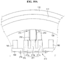
- the first sound generator may comprise: a bobbin disposed on the surface of the first substrate; a voice coil which surrounds the bobbin; a magnet disposed on the bobbin and spaced apart from the bobbin; and a lower plate disposed on the magnet and fixed to the lower cover or the circuit board by a fixing member.
- the display device may further include: a third sound generator disposed on the surface of the first substrate; and a sound circuit board electrically connected to the third sound generator to transmit a sound signal to the third sound generator.
- the third sound generator may include: a first electrode which receives a first driving voltage; a second electrode which receives a second driving voltage; and a vibration layer disposed between the first electrode and the second electrode, where the vibration layer includes a piezoelectric element which contracts or expands in response to the first driving voltage applied to the first electrode and the second driving voltage applied to the second electrode.
- the display device may further include: flexible films connected to the first substrate of the display panel; a source circuit board connected to the flexible films; and a cable which connects the circuit board and the source circuit board to each other.
- a first hole may be defined through the lower cover, and the cable may be disposed through the first hole.
- the source circuit board may be disposed on the surface of the first substrate, and the circuit board may be disposed on the first surface of the lower cover.
- a second hole may be defined through the lower cover, and the sound circuit board may be disposed or connected through the second hole.
- the source circuit board and the circuit board may be disposed on the first surface of the lower cover.
- the display device may further include a second buffer member which overlaps the third sound generator, where the second buffer member and the third sound generator are spaced apart from each other with a gap therebetween.
- the display device may further include a second buffer member disposed on the third sound generator, where the second buffer member and the lower cover are spaced apart from each other with a gap therebetween.
- a display device includes: a display panel including a first substrate; a lower cover disposed on a surface of the first substrate; a first sound generator disposed on the surface of the first substrate, where the first sound generator vibrates the display panel to output a sound; and a first buffer member disposed on the surface of the first substrate, where a height of the first buffer member is equal to or less than a distance between the first substrate and the lower cover.
- relative terms such as “lower” or “bottom” and “upper” or “top,” may be used herein to describe one element's relationship to another elements as illustrated in the Figures. It will be understood that relative terms are intended to encompass different orientations of the device in addition to the orientation depicted in the Figures. For example, if the device in one of the figures is turned over, elements described as being on the “lower” side of other elements would then be oriented on “upper” sides of the other elements. The exemplary term “lower,” can therefore, encompasses both an orientation of “lower” and “upper,” depending on the particular orientation of the figure.
- Exemplary embodiments are described herein with reference to cross section illustrations that are schematic illustrations of idealized embodiments. As such, variations from the shapes of the illustrations as a result, for example, of manufacturing techniques and/or tolerances, are to be expected. Thus, embodiments described herein should not be construed as limited to the particular shapes of regions as illustrated herein but are to include deviations in shapes that result, for example, from manufacturing. For example, a region illustrated or described as flat may, typically, have rough and/or nonlinear features. Moreover, sharp angles that are illustrated may be rounded. Thus, the regions illustrated in the figures are schematic in nature and their shapes are not intended to illustrate the precise shape of a region and are not intended to limit the scope of the present claims.
- a display device 10 is an organic light emitting display device using organic light emitting elements as light emitting elements, but the disclosure is not limited thereto.
- the display device 10 may be an inorganic light emitting display device using micro-light emitting diodes or inorganic semiconductors (inorganic light emitting diodes) as light emitting elements.
- FIG. 1 is a perspective view of a display device 10 according to an embodiment.
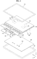
- FIG. 2 is an exploded perspective view of the display device 10 according to an embodiment.
- an embodiment of the display device 10 includes a set cover 100, a display panel 110, source driving circuits 121, flexible films 122, a heat dissipation film 130, source circuit boards 140, cables 150, a control circuit board 160, a timing control circuit 170, and a lower cover 180.
- the terms “upper”, “top” and “upper surface” indicate a direction in which a second substrate 112 is disposed with respect to a first substrate 111 of the display panel 110, that is, a Z-axis direction
- the terms “lower,” “bottom” and “lower surface” indicate a direction in which the heat dissipation film 130 is disposed with respect to the first substrate 111 of the display panel 110, that is, a direction opposite to the Z-axis direction.
- “left,” “right,” “up” and “down” indicate directions when the display panel 110 is viewed in a plane. For example, “left” indicates an X-axis direction, “right” indicates a direction opposite to the X-axis direction, “up” indicates a Y-axis direction, and “down” indicates a direction opposite to the Y-axis direction.
- the set cover 100 may surround or cover edges of the display panel 110.
- the set cover 100 may cover a non-display area excluding a display area of the display panel 110.
- the set cover 100 may include an upper set cover 101 and a lower set cover 102 as illustrated in FIG. 2 .
- the upper set cover 101 may cover edge portions of an upper surface of the display panel 110, and the lower set cover 102 may cover lower and side surfaces of the display panel 110.
- the upper set cover 101 and the lower set cover 102 may be coupled to each other by a fixing member such as a screw or an adhesive member such as a double-sided tape or an adhesive.
- the upper set cover 101 and the lower set cover 102 may include or be made of a plastic, a metal or a combination thereof.
- the display panel 110 may be rectangular in a plan view.
- the display panel 110 may have a rectangular planar shape having long sides in a first direction (X-axis direction) and short sides in a second direction (Y-axis direction) as illustrated in FIG. 2 .
- Each corner where a long side extending in the first direction (X-axis direction) meets a short side extending in the second direction (Y-axis direction) may be right-angled or may be rounded with a predetermined curvature.
- the planar shape of the display panel 110 is not limited to the rectangular shape, but may also be variously modified to have another polygonal shape, a circular shape or an elliptical shape.
- the display panel 110 is flat. However, the disclosure is not limited to this case.
- the display panel 110 may also be curved or bent with a predetermined curvature.
- the display panel 110 may include the first substrate 111 and the second substrate 112.
- the first substrate 111 and the second substrate 112 may be rigid or flexible.
- the first substrate 111 may include or be made of a glass or a plastic
- the second substrate 112 may include or be made of glass, plastic, an encapsulation film, or a barrier film.
- the plastic may be polyethersulphone (“PES”), polyacrylate (“PA”), polyarylate (“PAR”), polyetherimide (“PEI”), polyethylene naphthalate (“PEN”), polyethylene terepthalate (“PET”), polyphenylene sulfide (“PPS”), polyallylate, polyimide (“PI”), polycarbonate (“PC”), cellulose triacetate (“CAT”), cellulose acetate propionate (“CAP”), or a combination thereof.
- PES polyethersulphone
- PA polyacrylate
- PAR polyarylate
- PEI polyetherimide
- PEN polyethylene naphthalate
- PET polyethylene terepthalate
- PPS polyphenylene sulfide
- PI polyallylate
- PI polyimide
- PC polycarbonate
- CAT cellulose triacetate
- CAP cellulose acetate propionate
- CAP cellulose acetate propionate
- the display panel 110 may include a thin-film transistor layer TFTL, a light emitting element layer EML, a filler FL, a light wavelength conversion layer QDL, and a color filter layer CFL as illustrated in FIG. 7 .
- the first substrate 111 may be a thin-film transistor substrate on which the thin-film transistor layer TFTL, the light emitting element layer EML and a thin-film encapsulation layer 345 are disposed
- the second substrate 112 may be a color filter substrate on which the wavelength conversion layer QDL and the color filter layer CFL are disposed
- the filler FL may be disposed between the thin-film encapsulation layer 345 on the first substrate 111 and the wavelength conversion layer QDL on the second substrate 112.
- the thin-film transistor layer TFTL, the light emitting element layer EML, the filler FL, the wavelength conversion layer QDL and the color filter layer CFL of the display panel 110 (collectively shown as a layer 113 in FIG. 5 ) will be described in detail later with reference to FIG. 7 .
- an additional film 114 may be disposed on the second substrate 112.
- the additional film 114 may be an antireflective film.
- a side of each of the flexible films 122 may be attached onto a surface of an element on the first substrate 111 of the display panel 110, and the other side of each of the flexible films 122 may be attached onto a surface of one of the source circuit boards 140.
- the first substrate 111 is larger in size than the second substrate 112
- a side of an element on the first substrate 111 may be exposed without being covered by the second substrate 112.
- the flexible films 122 may be attached to the exposed side of an element on the first substrate 111 which is not covered by the second substrate 112.
- Each of the flexible films 122 may be attached onto the surface of the first substrate 111 and the surface of one of the source circuit boards 140 by using an anisotropic conductive film.
- Each of the flexible films 122 may be a tape carrier package or a chip on film. Each of the flexible films 122 is bendable. Therefore, the flexible films 122 may be bent toward a lower surface of the first substrate 111 as illustrated in FIGS. 4 and 6 . In such an embodiment, the source circuit boards 140, the cables 150, and the control circuit board 160 may be disposed on the lower surface of the first substrate 111.
- eight flexible films 122 are on the first substrate 111 of the display panel 110, but the number of the flexible films 122 is not limited thereto.
- the source driving circuits 121 may be disposed or mounted on surfaces of the flexible films 122, respectively.
- the source driving circuits 121 may be defined by or formed as integrated circuits.
- the source driving circuits 121 convert digital video data into analog data voltages based on a source control signal of the timing control circuit 170 and supply the analog data voltages to data lines of the display panel 110 through the flexible films 122.
- Each of the source circuit boards 140 may be connected to the control circuit board 160 via the cables 150.
- each of the source circuit boards 140 may include first connectors 151a for connection to the cables 150.
- the source circuit boards 140 may be flexible printed circuit boards or printed circuit boards.
- the cables 150 may be flexible cables.
- the control circuit board 160 may be connected to the source circuit boards 140 via the cables 150.
- the source circuit boards 140 may include first connectors 151 for connection to the cables 150
- the control circuit board 160 may include second connectors 152 for connection to the cables 150.
- the control circuit board 160 may be a flexible printed circuit board or a printed circuit board.
- four cables 150 connect the source circuit boards 140 and the control circuit board 160, but the number of the cables 150 is not limited thereto.
- the number of the cables 150 is not limited thereto.
- two source circuit boards 140 are illustrated, but the number of the source circuit boards 140 is not limited thereto.
- the timing control circuit 170 may be disposed or mounted on a first surface of the control circuit board 160.
- the timing control circuit 170 may be defined by or formed as an integrated circuit.
- the timing control circuit 170 may receive digital video data and timing signals from a system on chip of a system circuit board and generate a source control signal for controlling the timings of the source driving circuits 121 based on the timing signals.
- the system on chip may be disposed or mounted on the system circuit board connected to the control circuit board 160 via another flexible cable and may be defined by or formed as an integrated circuit.
- the system on chip may be a processor of a smart television, a central processing unit ("CPU") or graphics card of a computer or notebook, or an application processor of a smartphone or tablet personal computer (“PC").
- the system circuit board may be a flexible printed circuit board or a printed circuit board.
- a power supply circuit may be additionally attached onto the first surface of the control circuit board 160.
- the power supply circuit may generate voltages used for driving the display panel 110 from main power received from the system circuit board and supply the generated voltages to the display panel 110.
- the power supply circuit may generate a high-potential voltage, a low-potential voltage and an initialization voltage for driving organic light emitting elements and supply the generated voltages to the display panel 110.
- the power supply circuit may generate driving voltages for driving the source driving circuits 121, the timing control circuit 170, etc. and supply the generated voltages.
- the power supply circuit may be defined by or formed as an integrated circuit.
- the power supply circuit may be disposed on a power circuit board formed separately from the control circuit board 160.
- the power circuit board may be a flexible printed circuit board or a printed circuit board.
- the heat dissipation film 130 may be disposed on a surface of the first substrate 111 which does not face the second substrate 112, that is, on the lower surface of the first substrate 111.
- first through fourth sound generators 210 through 240 may be disposed on a surface of the heat dissipation film 130 which does not face the first substrate 111, that is, on a lower surface of the heat dissipation film 130.
- the heat dissipation film 130 dissipates heat generated by the first through fourth sound generators 210 through 240.
- the heat dissipation film 130 may include a layer including a material having high thermal conductivity, such as graphite, silver (Ag), copper (Cu) or aluminum (Al).
- the heat dissipation film 130 may include a plurality of graphite layers or a plurality of metal layers formed in the first direction (X-axis direction) and the second direction (Y-direction), not in a third direction (Z-direction).
- the heat generated by the first through fourth sound generators 210 through 240 is allowed to be diffused in the first direction (X-axis direction) and the second direction (Y-axis direction), the heat may be released more effectively.
- the first direction (X-axis direction) may be a width direction (or a horizontal direction) of the display panel 110
- the second direction (Y-axis direction) may be a length direction (or a vertical direction) of the display panel 110
- the third direction (Z-axis direction) may be a thickness direction of the display panel 110. Therefore, the heat dissipation film 130 may minimize the effect of the heat generated by the first through fourth sound generators 210 through 240 on the display panel 110.
- a thickness D1 of the heat dissipation film 130 may be greater than a thickness D2 of the first substrate 111 and a thickness D3 of the second substrate 112 to effectively prevent the heat generated by the first through fourth sound generators 210 through 240 from affecting the display panel 110.
- the size of the heat dissipation film 130 may be smaller than that of the first substrate 111. Therefore, an edge of the surface of the first substrate 111 may be exposed without being covered by the heat dissipation film 130.
- the heat dissipation film 130 may be omitted, and in such an embodiment, elements disposed on the surface of the heat dissipation film 130 can be understood as being disposed on the surface of the first substrate 111.
- the first through fourth sound generators 210 through 240 may be vibration devices capable of vibrating the display panel 110 in the third direction (Z-axis direction).
- the display panel 110 may serve as a diaphragm for outputting sound.
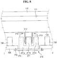
- each of the first sound generator 210 and the second sound generator 220 may be an exciter that vibrates the display panel 110 by generating a magnetic force using a voice coil as illustrated in FIGS. 8 , 10A and 10B .
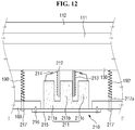
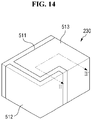
- each of the third sound generator 230 and the fourth sound generator 240 may be a piezoelectric element that vibrates the display panel 110 by contracting or expanding in response to an applied voltage as illustrated in FIGS. 12 , 13 , 14 , 15A and 15B .
- the first sound generator 210 and the second sound generator 220 may serve as mid- and low-sound generators that output sound in mid and low bands
- the third sound generator 230 and the fourth sound generator 240 may serve as high-sound generators that output sound in a high band higher than that of the sound output by the first sound generator 210 and the second sound generator 220.
- the display device 10 may provide right stereo sound using the first sound generator 210 and the third sound generator 230 and provide left stereo sound using the second sound generator 220 and the fourth sound generator 240. Therefore, the display device 10 may provide 2.0 channel stereo sound.
- the third sound generator 230 and the fourth sound generator 240 may be omitted, and the first sound generator 210 and the second sound generator 220 may respectively serve or function as mid- and high-sound generators that output sound in mid and high bands.
- the display device 10 may provide right stereo sound using the first sound generator 210 and provide left stereo sound using the second sound generator 220. Therefore, the display device 10 may provide 2.0 channel stereo sound.
- the second sound generator 220 may be omitted, the first sound generator 210 may serve as a low-sound generator that outputs sound in a low band, and the third sound generator 230 and the fourth sound generator 240 may serve as high-sound generators that output sound in a high band higher than that of the sound output by the first sound generator 210.
- the display device 10 may provide low-pitched sound using the first sound generator 210, provide right stereo sound using the third sound generator 230 and provide left stereo sound using the fourth sound generator 240. Therefore, the display device 10 may provide 2.1 channel stereo sound.
- the second sound generator 220, the third sound generator 230 and the fourth sound generator 240 may be omitted, and the first sound generator 210 may serve as a mid- and high-sound generator that outputs sound in mid and high bands.
- the display device 10 may provide mid- and high-pitched sound using the first sound generator 210. Therefore, the display device 10 may provide monaural sound.
- the display device 10 includes four sound generators 210 through 240 as shown in FIG. 2 , but the number of the sound generators 210 through 240 is not limited thereto.
- the first sound generator 210 and the second sound generator 220 will be described in detail later with reference to FIGS. 8 , 10A and 10B .
- the third sound generator 230 and the fourth sound generator 240 will be described in detail later with reference to FIGS. 12 , 13 , 14 , 15A and 15B .
- the lower cover 180 may be disposed on the surface of the heat dissipation film 130.
- the lower cover 180 may be attached to the edges of the surface of the first substrate 111 of the display panel 110 with a first adhesive member 115.
- the first adhesive member 115 may be a double-sided tape including a buffer layer such as foam.
- the lower cover 180 may be metal or tempered glass.
- the display device 10 outputs sound using the display panel 110 as a diaphragm through the first through fourth sound generators 210 through 240.
- the first through fourth sound generators 210 through 240 allow a speaker typically provided on a lower surface or a side of a conventional display panel to be omitted.
- the display device 10 may be a medium- and large-sized display device including a plurality of source driving circuits 121 in FIGS. 1 and 2 , but the disclosure is not limited thereto.
- the display device may also be a small-sized display device including a single source driving circuit 121.
- the flexible films 122, the source circuit boards 140, and the cables 150 may be omitted.
- the source driving circuits 121 and the timing control circuit 170 may be integrated into a single integrated circuit and then attached onto a single flexible circuit board or disposed on the first substrate 111 of the display panel 110.
- the medium- and large-sized display device include monitors and televisions, for example, and the small-sized display device include smartphones and tablet PCs, for example.
- FIG. 3 is a bottom view of an embodiment of the display device 10 of FIG. 2 .
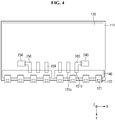
- FIG. 4 is a bottom view of an embodiment of the display device 10 when the lower cover 180 and the control circuit board 160 are omitted from FIG. 3 .
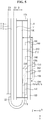
- FIG. 5 is a side view of an embodiment of the display device 10 of FIG. 2 .
- the flexible films 122 may be bent toward the lower surface of the heat dissipation film 130. Therefore, the source circuit boards 140 may be disposed on the surface of the heat dissipation film 130.
- the control circuit board 160 is disposed on a first surface of the lower cover 180.
- the source circuit boards 140 are disposed between the surface of the heat dissipation film 130 and a second surface of the lower cover 180. Therefore, the cables 150 connected to the first connectors 151a of the source circuit boards 140 may be connected to the second connectors 152 of the control circuit board 160 through first cable holes CH1 defined through the lower cover 180.
- the third sound generator 230 and the fourth sound generator 240 may be attached onto the surface of the heat dissipation film 130 with an adhesive member such as a double-sided adhesive.
- the third sound generator 230 may be connected to a second connector 151b of a source circuit board 140 by a first sound circuit board 250
- the fourth sound generator 240 may be connected to a second connector 151b of a source circuit board 140 by a second sound circuit board 260.
- a first pad and a second pad, which are connected to a first electrode and a second electrode disposed on a surface of the third sound generator 230, may be disposed on a side of the first sound circuit board 250.
- a first pad and a second pad, which are connected to a first electrode and a second electrode disposed on a surface of the fourth sound generator 240, may be disposed on a side of the second sound circuit board 260.
- Connection portions for connection to the second connectors 151b of the source circuit boards 140 may be disposed on the other side of the first sound circuit board 250 and the other side of the second sound circuit board 260. That is, the third sound generator 230 may be electrically connected to the source circuit board 140 by the first sound circuit board 250, and the fourth sound generator 240 may be electrically connected to the source circuit board 140 by the second sound circuit board 260.
- the first sound circuit board 250 and the second sound circuit board 260 may be flexible printed circuit boards or flexible cables.
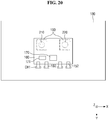
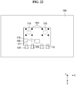
- a sound driving circuit 171, the first sound generator 210, and the second sound generator 220 as well as the timing control circuit 170 may be disposed on the control circuit board 160.
- the sound driving circuit 171 may receive a sound control signal, which is a digital signal, from the system circuit board.
- the sound driving circuit 171 may be defined by or formed as an integrated circuit and may be disposed on the control circuit board 160 or the system circuit board.
- the sound driving circuit 171 may include a digital signal processor ("DSP") for processing a sound control signal which is a digital signal, a digital-to-analog converter (“DAC”) for converting the digital signal processed by the DSP into driving voltages which are analog signals, and an amplifier (“AMP”) for amplifying the analog driving voltages output from the DAC and outputting the amplified analog driving voltages.
- the analog driving voltages may include a positive driving voltage and a negative driving voltage.
- the sound driving circuit 171 may generate a first sound signal including a first driving voltage (hereinafter, (1A) th driving voltage) and a second first driving voltage (hereinafter, (1B) th driving voltage) for driving the first sound generator 210, and a second sound signal including a first second driving voltage (hereinafter, (2A) th driving voltage) and a second second driving voltage (hereinafter (2B) th driving voltage) for driving the second sound generator 220 in response to a sound control signal.
- a first sound signal including a first driving voltage (hereinafter, (1A) th driving voltage) and a second first driving voltage (hereinafter, (1B) th driving voltage) for driving the first sound generator 210
- a second sound signal including a first second driving voltage (hereinafter, (2A) th driving voltage) and a second second driving voltage (hereinafter (2B) th driving voltage) for driving the second sound generator 220 in response to a sound control signal.
- the sound driving circuit 171 may generate a third sound signal including a first third driving voltage (hereinafter (3A) th driving voltage) and a second third driving voltage (hereinafter, (3B) th driving voltage) for driving the third sound generator 230, and a fourth sound signal including a first fourth driving voltage (hereinafter, (4A) th driving voltage) and a second fourth driving voltage (hereinafter, (4B) th driving voltage) for driving the fourth sound generator 240 in response to the sound control signal.
- a third sound signal including a first third driving voltage (hereinafter (3A) th driving voltage) and a second third driving voltage (hereinafter, (3B) th driving voltage) for driving the third sound generator 230
- a fourth sound signal including a first fourth driving voltage (hereinafter, (4A) th driving voltage) and a second fourth driving voltage (hereinafter, (4B) th driving voltage) for driving the fourth sound generator 240 in response to the sound control signal.
- the first sound generator 210 may receive the first sound signal including the (1A) th driving voltage and the (1B) th driving voltage from the sound driving circuit 171.
- the first sound generator 210 may output sound by vibrating the display panel 110 based on the (1A) th driving voltage and the (1B) th driving voltage.
- the second sound generator 220 may receive the second sound signal including the (2A) th driving voltage and the (2B) th driving voltage from the sound driving circuit 171.
- the second sound generator 220 may output sound by vibrating the display panel 110 based on the (2A) th driving voltage and the (2B) th driving voltage.
- the sound driving circuit 171 and the first sound generator 210 may be electrically connected to each other by metal lines of the control circuit board 160.
- the sound driving circuit 171 and the second sound generator 220 may be electrically connected to each other by metal lines of the control circuit board 160.
- the third sound generator 230 may receive the third sound signal including the (3A) th driving voltage and the (3B) th driving voltage from the sound driving circuit 171.
- the third sound generator 230 may output sound by vibrating the display panel 110 based on the (3A) th driving voltage and the (3B) th driving voltage.
- the fourth sound generator 240 may receive the fourth sound signal including the (4A) th driving voltage and the (4B) th driving voltage from the sound driving circuit 171.
- the fourth sound generator 240 may output sound by vibrating the display panel 110 based on the (4A) th driving voltage and the (4B) th driving voltage.
- the number of sound generators implemented as exciters and the number of sound generators implemented as piezoelectric elements are not limited to those illustrated in FIGS. 3 through 5 .
- the sound driving circuit 171 may be disposed on the control circuit board 160 as illustrated in FIG. 3 , and the third sound generator 230 and the fourth sound generator 240 may be disposed on the surface of the heat dissipation film 130.
- the third sound signal of the sound driving circuit 171 may be transmitted to the third sound generator 230 via a cable 150, the source circuit board 140, and the first sound circuit board 250.
- the fourth sound signal of the sound driving circuit 171 may be transmitted to the fourth sound generator 240 via a cable 150, the source circuit board 140, and the second sound circuit board 260.
- a first buffer member 190 effectively prevents the display panel 110 from colliding with the lower cover 180 and being damaged due to large vibration displacement of the display panel 110 when the display panel 110 is vibrated by the first sound generator 210 and by the second sound generator 220.
- the first buffer member 190 may surround each of the first sound generator 210 and the second sound generator 220.
- the first buffer member 190 may surround each of the first sound generator 210 and the second sound generator 220 in a circular shape when seen in a plan view.
- a distance between the first buffer member 190 and the first sound generator 210 and between the first buffer member 190 and the second sound generator 220 may be substantially constant.
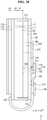
- the first buffer member 190 may be attached to a second surface of the control circuit board 160 or the second surface of the lower cover 180 as illustrated in FIG. 5 .
- the first buffer member 190 may be attached onto the surface of the heat dissipation film 130 as illustrated in FIG. 31 .
- the height of the first buffer member 190 is less than the distance between the surface of the heat dissipation film 130 and the second surface of the control circuit board 160.
- the first buffer member 190 and the heat dissipation film 130 is spaced apart from each other with a gap therebetween.
- the height of the first buffer member 190 may be less than a height HI of the first sound generator 210 and a height of the second sound generator 220.
- the height HI of the first sound generator 210 may be a distance from a bobbin 212 of the first sound generator 210 to a lower plate thereof as illustrated in FIG. 5 .
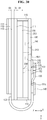
- the first buffer member 190 may be attached to the surface of the heat dissipation film 130 and the second surface of the control circuit board 160 or the second surface of the lower cover 180 as illustrated in FIG. 32 .
- the height of the first buffer member 190 may be substantially equal to the distance between the surface of the heat dissipation film 130 and the second surface of the control circuit board 160.
- a second buffer member 190c effectively prevents the display panel 110 from colliding with the lower cover 180 and being damaged due to substantial vibration displacement of the display panel 110 when the display panel 110 is vibrated by the third sound generator 230 and the fourth sound generator 240.
- the second buffer member 190c may overlap the third sound generator 230 and the fourth sound generator 240.
- the second buffer member 190c may be attached to the second surface of the lower cover 180 or the second surface of the control circuit board 160 as illustrated in FIG. 5 .
- the second buffer member 190c may be disposed on the surface of the third sound generator 230 and the surface of the fourth sound generator 240.
- the height of the second buffer member 190c may be less than that of the first buffer member 190. In such an embodiment, the height of the second buffer member 190c is less than the distance between the first surface of the heat dissipation film 130 and the second surface of the control circuit board 160 or the second surface of the lower cover 180. Therefore, in an embodiment where the second buffer member 190c is attached to the second surface of the lower cover 180 or the second surface of the control circuit board 160 as illustrated in FIG. 5 , a gap may exist between the second buffer member 190c and the third sound generator 230 and between the second buffer member 190c and the fourth sound generator 240. Alternatively, in an embodiment where the second buffer member 190c is disposed on the surface of the third sound generator 230 and the surface of the fourth sound generator 240, there may a gap between the second buffer member 190c and the control circuit board 160 or the lower cover 180.
- the third sound generator 230 and the source circuit board 140 are connected by the first sound circuit board 250, and the fourth sound generator 240 and the source circuit board 140 are connected by the second sound circuit board 260. Therefore, in an embodiment where the third sound generator 230 and the fourth sound generator 240 are disposed on the surface of the heat dissipation film 130 while the control circuit board 160 is disposed on the first surface of the lower cover 180, the control circuit board 160 and the third sound generator 230 may be easily or effectively electrically connected to each other, and the control circuit board 160 and the fourth sound generator 240 may be easily or effectively electrically connected to each other.
- FIG. 6 is a bottom view of the heat dissipation film 130, the adhesive member 115, a blocking member 200 and the first through fourth sound generators 210 through 240 of the display device.
- FIG. 6 only the first substrate 111, the first adhesive member 115, the heat dissipation film 130, the blocking member 200 and the first through fourth sound generators 210 through 240 of the display panel 110 are illustrated for ease of description. That is, the source driving circuits 121, the flexible films 122, the source circuit boards 140, the cables 150, the control circuit board 160, the timing control circuit 170 and the lower cover 180 are omitted from FIG. 6 .
- the size of the heat dissipation film 130 may be smaller than that of the first substrate 111. Therefore, four edges of the surface of the first substrate 111 may be exposed without being covered by the heat dissipation film 130.
- the first adhesive member 115 may be disposed on the exposed four edges of the surface of the first substrate 111 which are not covered by the heat dissipation film 130.
- the first adhesive member 115 may attach the surface of the first substrate 111 to the second surface of the lower cover 180 as illustrated in FIG. 5 .
- the first adhesive member 115 may be a double-sided tape including a buffer layer such as a foam.
- the blocking member 200 may block the propagation of vibrations of the display panel 110 generated by each of the first through fourth sound generators 210 through 240 or block the transmission of sound generated by the vibration of the display panel 110.
- the blocking member 200 may be attached to the surface of the heat dissipation film 130 and the second surface of the lower cover 180 to block the propagation of vibrations of the display panel 110 or the transmission of sound.
- the blocking member 200 may be disposed on four edge portions of the heat dissipation film 130.
- the blocking member 200 may attach the surface of the heat dissipation film 130 to the second surface of the lower cover 180.
- the height of the blocking member 200 is greater than the height of the first buffer member 190 and the height of the second buffer member 190c.
- the surface of the heat dissipation film 130 may be divided into first through sixth areas A1 through A6 by the blocking member 200 as illustrated in FIG. 6 .
- the first area A1 is an area where the first sound generator 210 is disposed and may be defined by the blocking member 200 disposed to surround the first sound generator 210.
- the second area A2 is an area where the second sound generator 220 is disposed and may be defined by the blocking member 200 disposed to surround the second sound generator 220.
- the size of the first area A1 and the size of the second area A2 may be substantially the same as each other.
- the third area A3 is an area where the third sound generator 230 is disposed and may be defined by the blocking member 200 disposed to surround the third sound generator 230.
- the fourth area A4 is an area where the fourth sound generator 240 is disposed and may be defined by the blocking member 200 disposed to surround the four sound generator 240.
- the size of the third area A3 and the size of the fourth area A4 may be smaller than the size of the first area A1 and the size of the second are A2, respectively.
- the fifth area A5 is an area where the source circuit boards 140 are disposed and may be defined by the blocking member 200 disposed to surround the source circuit boards 140.
- the fifth area A5 may effectively prevent or substantially reduce the effect of the first through fourth sound generators 210 through 240 of the first through fourth areas A1 through A4 on the source circuit boards 140, the source driving circuits 121 and the flexible films 122.
- the sixth area A6 is an area between the first area A1 and the second area A2. No sound generator may be disposed in the sixth area A6.
- the sixth area A6 may increase the distance between the first area A1 and the second area A2. Therefore, in such an embodiment, the effect of vibrations of the display panel 110 generated by the first sound generator 210 of the first area A1 on vibrations of the display panel 110 generated by the second sound generator 220 of the second area A2 or the effect of vibrations of the display panel 110 generated by the second sound generator 220 of the second area A2 on vibrations of the display panel 110 generated by the first sound generator 210 of the first area A1 may be effectively prevented or substantially reduced.
- the sixth area A6 may be omitted, and the first area A1 and the second area A2 may be disposed adjacent to each other.
- each of the first through fourth sound generators 210 through 240 is surrounded by the blocking member 200. Therefore, the effect of vibrations of the display panel 110 generated by each of the first through fourth sound generators 210 through 240 on vibrations of the display panel 110 generated by an adjacent sound generator may be effectively prevented or substantially reduced.
- FIG. 7 is a cross-sectional view of an embodiment of the display area of the display panel 110.
- an embodiment of the display panel 110 may include the first substrate 111, the second substrate 112, the thin-film transistor layer TFTL, the light emitting element layer EML, the filler FL, the wavelength conversion layer QDL, and the color filter layer CFL.
- a buffer layer 302 may be disposed on a surface of the first substrate 111 which faces the second substrate 112.
- the buffer layer 302 may be disposed on the first substrate 111 to protect thin-film transistors 335 and light emitting elements from moisture that may be introduced through the first substrate 111 which may be vulnerable to moisture penetration.
- the buffer layer 302 may include or be composed of a plurality of inorganic layers stacked alternately.
- the buffer layer 302 may be a multilayer in which one or more inorganic layers including at least one selected from a silicon oxide (SiOx) layer, a silicon nitride (SiNx) layer and SiON are alternately stacked.
- the buffer layer 302 may be omitted.
- the thin-film transistor layer TFTL is disposed on the buffer layer 302.
- the thin-film transistor layer TFTL includes the thin-film transistors 335, a gate insulating layer 336, an interlayer insulating film 337, a protective layer 338, and a planarization layer 339.
- the thin-film transistors 335 are disposed on the buffer layer 302.
- Each of the thin-film transistors 335 includes an active layer 331, a gate electrode 332, a source electrode 333, and a drain electrode 334.
- each of the thin-film transistors 335 is a top-gate type in which the gate electrode 332 is located above the active layer 331, but the disclosure is not limited thereto.
- each of the thin-film transistors 335 may also be a bottom-gate type in which the gate electrode 332 is located under the active layer 331 or a double-gate type in which the gate electrode 332 is located both above and under the active layer 331.
- the active layers 331 are disposed on the buffer layer 302.
- the active layers 331 may include or be made of a silicon-based semiconductor material or an oxide-based semiconductor material.
- a light shielding layer may be disposed between the buffer layer 302 and the active layers 331 to block external light from entering the active layers 331.
- the gate insulating layer 336 may be disposed on the active layers 331.
- the gate insulating layer 336 may be an inorganic layer, for example, a SiOx layer, a SiNx layer, or a multilayer including or composed of these layers.
- the gate electrodes 332 and gate lines may be disposed on the gate insulating layer 336.
- Each of the gate electrodes 332 and the gate lines may be a single layer or a multilayer including or made of any one or more of molybdenum (Mo), aluminum (Al), chromium (Cr), gold (Au), titanium (Ti), nickel (Ni), neodymium (Ne), copper (Cu), and an alloy thereof.
- the interlayer insulating film 337 may be disposed on the gate electrodes 332 and the gate lines.
- the interlayer insulating film 337 may be an inorganic layer, for example, a SiOx layer, a SiNx layer, or a multilayer including or composed of these layers.
- the source electrodes 333, the drain electrodes 334, and data lines may be disposed on the interlayer insulating film 337.
- Each of the source electrodes 333 and the drain electrodes 334 may be connected to an active layer 331 through a contact hole defined through the gate insulating layer 336 and the interlayer insulating film 337.
- Each of the source electrodes 333, the drain electrodes 334 and the data lines may be a single layer or a multilayer including or made of any one or more of molybdenum (Mo), aluminum (Al), chromium (Cr), gold (Au), titanium (Ti), nickel (Ni), neodymium (Ne), copper (Cu), and an alloy thereof.
- the protective layer 338 for insulating the thin-film transistors 335 may be disposed on the source electrodes 333, the drain electrodes 334, and the data lines.
- the protective layer 338 may be an inorganic layer, for example, a SiOx layer, a SiNx layer, or a multilayer including or composed of these layers.
- the planarization layer 339 may be disposed on the protective layer 338 to planarize steps due to the thin-film transistors 335.
- the planarization layer 339 may include or be made of an organic layer such as acryl resin, epoxy resin, phenolic resin, polyamide resin, or polyimide resin.
- the light emitting element layer EML is disposed on the thin-film transistor layer TFTL.
- the light emitting element layer EML includes light emitting elements and a pixel defining layer 344.
- the light emitting elements and the pixel defining layer 344 are disposed on the planarization layer 339.
- the light emitting elements may be organic light emitting elements.
- each of the light emitting elements may include an anode 341, a light emitting layer 342, and a cathode 343.
- the anodes 341 may be disposed on the planarization layer 339.
- the anodes 341 may be connected to the drain electrodes 334 of the thin-film transistors 335 through contact holes defined through the protective layer 338 and the planarization layer 339.
- the pixel defining layer 344 may be disposed on the planarization layer 339 and may cover edges of the anodes 341 to define pixels.
- the pixel defining layer 344 defines subpixels PX1 through PX3.
- Each of the subpixels PX1 through PX3 is an area in which the anode 341, the light emitting layer 342 and the cathode 343 are sequentially stacked so that holes from the anode 341 and electrons from the cathode 343 combine together in the light emitting layer 342 to emit light.
- the light emitting layer 342 is disposed on the anodes 341 and the pixel defining layer 344.
- the light emitting layer 342 may be an organic light emitting layer.
- the light emitting layer 342 may emit light having a short wavelength, such as a blue light or an ultraviolet light.
- the blue light may have a peak wavelength range of about 450 nanometers (nm) to about 490 nm, and the ultraviolet light may have a peak wavelength range of less than about 450 nm.
- the light emitting layer 342 may be a common layer commonly disposed to cover all of the subpixels PX1 through PX3.
- the display panel 110 may include the wavelength conversion layer QDL for converting short-wavelength light such as a blue light or an ultraviolet light emitted from the light emitting layer 342 into a red light, a green light and a blue light and the color filter layer CFL which transmits each of the red light, the green light and the blue light.
- the wavelength conversion layer QDL for converting short-wavelength light such as a blue light or an ultraviolet light emitted from the light emitting layer 342 into a red light, a green light and a blue light
- the color filter layer CFL which transmits each of the red light, the green light and the blue light.
- the light emitting layer 342 may include a hole transporting layer, a light emitting layer, and an electron transporting layer.
- the light emitting layer 342 have a tandem structure of two or more stacks, where a charge generating layer may be formed between the stacks.
- the cathode 343 is disposed on the light emitting layer 342.
- the cathode 343 may be disposed to cover the light emitting layer 342.
- the cathode 343 may be a common layer commonly disposed to cover all pixels.
- the light emitting element layer EML may be a top emission type which emits light toward the second substrate 112, that is, in an upward direction.
- the anodes 341 may include or be made of a metal material having high reflectivity, such as a stacked structure (Ti/Al/Ti) of Al and Ti, a stacked structure (ITO/Al/ITO) of Al and indium tin oxide ("ITO"), an APC alloy, or a stacked structure (ITO/APC/ITO) of an APC alloy and ITO.
- the APC alloy is an alloy of Ag, palladium (Pd), and Cu.
- the cathode 343 may include or be made of a transparent conductive material (“TCO") capable of transmitting light, such as ITO or indium zinc oxide (“IZO"), or a semi-transmissive conductive material such as magnesium (Mg), Ag or an alloy of Mg and Ag.
- TCO transparent conductive material
- IZO indium zinc oxide
- Mg magnesium
- Ag silver
- Ag an alloy of Mg and Ag.
- the light output efficiency may be increased by a microcavity-effect.
- a thin-film encapsulation layer 345 is disposed on the light emitting element layer EML.
- the thin-film encapsulation layer 345 may prevent oxygen or moisture from permeating the light emitting layer 342 and the cathode 343.
- the thin-film encapsulation layer 345 may include at least one inorganic layer.
- the inorganic layer may include or be made of silicon nitride, aluminum nitride, zirconium nitride, titanium nitride, hafnium nitride, tantalum nitride, silicon oxide, aluminum oxide, or titanium oxide.
- the thin-film encapsulation layer 345 may further include at least one organic layer.
- the organic layer may have a sufficient thickness to prevent particles from penetrating the thin-film encapsulation layer 345 and entering the light emitting layer 342 and the cathode 343.
- the organic layer may include at least one of epoxy, acrylate, and urethane acrylate.
- the color filter layer CFL is disposed on a surface of the second substrate 112 which faces the first substrate 111.
- the color filter layer CFL may include a black matrix 360 and color filters 370.
- the black matrix 360 may be disposed on the surface of the second substrate 112.
- the black matrix 360 may not overlap the subpixels PX1 through PX3 and may overlap the pixel defining layer 344.
- the black matrix 360 may include black dye capable of blocking light or an opaque metal material.
- the color filters 370 may be disposed to overlap the subpixels PX1 through PX3.
- a first color filter 371 may overlap a first subpixel PX1, a second color filter 372 may overlap a second subpixel PX2, and a third color filter 373 may overlap a third subpixel PX3.
- the first color filter 371 may be a first color light transmitting filter that transmits light of a first color
- the second color filter 372 may be a second color light transmitting filter that transmits light of a second color
- the third color filter 373 may be a third color light transmitting filter that transmits light of a third color.
- the first color may be a red color
- the second color may be a green color
- the third color may be a blue color.
- the peak wavelength range of the red light transmitted through the first color filter 371 may be about 620 nm to about 750 nm
- the peak wavelength range of the green light transmitted through the second color filter 372 may be about 500 nm to about 570 nm
- the peak wavelength range of the blue light transmitted through the third color filter 373 may be about 450 nm to about 490 nm.
- edges of two adjacent color filters may overlap the black matrix 360. Therefore, the black matrix 360 may effectively prevent color mixing that occurs when light emitted from the light emitting layer 342 of a subpixel travels to a color filter of an adjacent subpixel.
- An overcoat layer may be disposed on the color filters 370 to planarize a step due to the black matrix 360. Alternatively, the overcoat layer may be omitted.
- the wavelength conversion layer QDL is disposed on the color filter layer CFL.
- the wavelength conversion layer QDL may include a first capping layer 351, a first wavelength conversion layer 352, a second wavelength conversion layer 353, a third wavelength conversion layer 354, a second capping layer 355, an interlayer organic film 356, and a third capping layer 357.
- the first capping layer 351 may be disposed on the color filter layer CFL.
- the first capping layer 351 may effectively prevent moisture or oxygen from permeating into the first wavelength conversion layer 352, the second wavelength conversion layer 353 and the third wavelength conversion layer 354 from the outside through the color filter layer CFL.
- the first capping layer 351 may include or be made of an inorganic layer such as silicon nitride, aluminum nitride, zirconium nitride, titanium nitride, hafnium nitride, tantalum nitride, silicon oxide, aluminum oxide, or titanium oxide.
- the first wavelength conversion layer 352, the second wavelength conversion layer 353 and the third wavelength conversion layer 354 may be disposed on the first capping layer 351.
- the first wavelength conversion layer 352 may overlap the first subpixel PX1.
- the first wavelength conversion layer 352 may convert short-wavelength light such as a blue light or an ultraviolet light emitted from the light emitting layer 342 of the first subpixel PX into light of the first color.
- the first wavelength conversion layer 352 may include a first base resin, a first wavelength shifter, and a first scatterer.
- the first base resin may be a material having high light transmittance and high dispersion characteristics for the first wavelength shifter and the first scatterer.
- the first base resin may include an organic material such as epoxy resin, acrylic resin, cardo resin, or imide resin.
- the first wavelength shifter may convert or shift the wavelength range of incident light.
- the first wavelength shifter may be quantum dots, a quantum rod, or a phosphor.
- the first wavelength shifter is quantum dots, which may be a semiconductor nanocrystalline material and have a specific band gap according to the composition and size thereof.
- the first wavelength shifter may absorb incident light and then emit light having a unique wavelength.
- the first wavelength shifter may have a core-shell structure including a core containing a nanocrystal and a shell surrounding the core.
- the nanocrystal that forms the core may include a group IV nanocrystal, a group II-VI compound nanocrystal, a group III-V compound nanocrystal, a group IV-VI nanocrystal, and combinations of the same.
- the shell may serve as a protective layer for maintaining semiconductor characteristics by preventing chemical denaturation of the core and/or as a charging layer for giving electrophoretic characteristics to the quantum dot.
- the shell may be a single layer or a multilayer.
- the shell may be, for example, a metal or non-metal oxide, a semiconductor compound, or a combination thereof.
- the first scatterer may have a refractive index different from that of the first base resin and form an optical interface with the first base resin.
- the first scatterer may be light scattering particles.
- the first scatterer may be metal oxide particles including titanium oxide (TiO 2 ), silicon oxide (SiO 2 ), zirconium oxide (ZrO 2 ), aluminum oxide (Al 2 O 3 ), indium oxide (In 2 O 3 ), zinc oxide (ZnO), or tin oxide (SnO 2 ).
- the first scatterer may be organic particles including acrylic resin or urethane resin.
- the first scatterer may scatter incident light in random directions without substantially changing the wavelength of the light transmitted through the first wavelength conversion layer 352. Accordingly, the first scatterer may increase the length of the path of the light transmitted through the first wavelength conversion layer 352, thereby increasing the color conversion efficiency of the first wavelength shifter.
- the first wavelength conversion layer 352 may overlap the first color filter 371. Therefore, a portion of short-wavelength light such as a blue light or an ultraviolet light provided from the first subpixel PX1 may pass through the first wavelength conversion layer 352 without being converted into light of the first color by the first wavelength shifter. In such an embodiment, the short-wavelength light such as a blue light or an ultraviolet light incident on the first color filter 371 without being converted by the first wavelength conversion layer 352 may not pass through the first color filter 371. In such an embodiment, light of the first color output from the first wavelength conversion layer 352 may pass through the first color filter 371 and proceed toward the second substrate 112.
- the second wavelength conversion layer 353 may overlap the second subpixel PX2.
- the second wavelength conversion layer 353 may convert short-wavelength light such as a blue light or an ultraviolet light emitted from the light emitting layer 342 of the second subpixel PX2 into light of the second color.
- the second wavelength conversion layer 353 may include a second base resin, a second wavelength shifter, and a second scatterer.
- the second base resin, the second wavelength shifter and the second scatterer of the second wavelength conversion layer 353 are substantially the same as those of the first wavelength conversion layer 352, and thus any repetitive detailed description thereof will be omitted.
- the diameter of the second wavelength shifter may be less than that of the first wavelength shifter.
- the second wavelength conversion layer 353 may overlap the second color filter 372. Therefore, a portion of short-wavelength light such as a blue light or an ultraviolet light provided from the second subpixel PX2 may pass through the second wavelength conversion layer 353 without being converted into light of the second color by the second wavelength shifter. In such an embodiment, the short-wavelength light such as a blue light or an ultraviolet light incident on the second color filter 372 without being converted by the second wavelength conversion layer 353 may not pass through the second color filter 372. In such an embodiment, light of the second color output from the second wavelength conversion layer 353 may pass through the second color filter 372 and proceed toward the second substrate 112.
- the third wavelength conversion layer 354 may overlap the third subpixel PX3.
- the third wavelength conversion layer 354 may convert short-wavelength light such as blue light or ultraviolet light emitted from the light emitting layer 342 of the third subpixel PX3 into light of the third color.
- the third wavelength conversion layer 354 may include a third base resin and a third scatterer.
- the third base resin and the third scatterer of the third wavelength conversion layer 354 are substantially the same as those of the first wavelength conversion layer 352, and thus any repetitive detailed description thereof will be omitted.
- the third wavelength conversion layer 354 may overlap the third color filter 373. Therefore, short-wavelength light such as a blue light or an ultraviolet light provided from the third subpixel PX3 may pass through the third wavelength conversion layer 354 as it is, and the light that passes through the third wavelength conversion layer 354 may pass through the third color filter 373 and proceed toward the second substrate 112.
- short-wavelength light such as a blue light or an ultraviolet light provided from the third subpixel PX3 may pass through the third wavelength conversion layer 354 as it is, and the light that passes through the third wavelength conversion layer 354 may pass through the third color filter 373 and proceed toward the second substrate 112.
- the second capping layer 355 may be disposed on the first wavelength conversion layer 352, the second wavelength conversion layer 353, the third wavelength conversion layer 354, and portions of the first capping layer 351 not covered by the wavelength conversion layers 352 through 354.
- the second capping layer 355 effectively prevents moisture or oxygen from permeating into the first wavelength conversion layer 352, the second wavelength conversion layer 353 and the third wavelength conversion layer 354 from the outside.
- the second capping layer 355 may include or be made of an inorganic layer such as silicon nitride, aluminum nitride, zirconium nitride, titanium nitride, hafnium nitride, tantalum nitride, silicon oxide, aluminum oxide, or titanium oxide.
- the interlayer organic film 356 may be disposed on the second capping layer 355.
- the interlayer organic film 356 may be a planarization layer for planarizing steps due to the wavelength conversion layers 352 through 354.
- the interlayer organic film 356 may include or be made of an organic layer such as acryl resin, epoxy resin, phenolic resin, polyamide resin, or polyimide resin.
- the third capping layer 357 may be disposed on the interlayer organic film 356.
- the third capping layer 357 may include or be made of an inorganic layer such as silicon nitride, aluminum nitride, zirconium nitride, titanium nitride, hafnium nitride, tantalum nitride, silicon oxide, aluminum oxide, or titanium oxide.
- the filler FL may be disposed between the thin-film encapsulation layer 345 disposed on the first substrate 111 and the third capping layer 357 disposed on the second substrate 112.
- the filler FL may include or be made of a material having a buffer function.
- the filler FL may include or be made of an organic layer such as acryl resin, epoxy resin, phenolic resin, polyamide resin, or polyimide resin.
- a sealing material for bonding the first substrate 111 and the second substrate 112 may be disposed in the non-display area of the display panel 110.
- the filler FL When seen in a plan view, the filler FL may be surrounded by the sealing material.
- the sealing material may be a glass frit or a sealant.
- the first through third subpixels PX1 through PX3 may emit short-wavelength light such as a blue light or an ultraviolet light.
- Light of the first subpixel PX1 is converted into light of the first color by the first wavelength conversion layer 352 and then output through the first color filter CF1.
- Light of the second subpixel PX2 is converted into light of the second color by the second wavelength conversion layer 353 and then output through the second color filter CF2.
- Light of the third subpixel PX3 is output through the third wavelength conversion layer 354 and the third color filter CF3. Therefore, white light may be output form the display area of the display panel 110.
- the subpixels PX1 through PX3 are a top emission type which emits light toward the second substrate 112, that is, in the upward direction. Therefore, the heat dissipation film 130 including an opaque material such as graphite or aluminum may be disposed on the surface of the first substrate 111.
- FIG. 8 is a cross-sectional view showing an embodiment of the first sound generator 210 and the second sound generator 220 of FIG. 3 .
- FIG. 8 is a cross-sectional view taken along line I-I' of FIG. 3 .
- each of the first sound generator 210 and the second sound generator 220 may be an exciter that vibrates the display panel 110 by generating a magnetic force using a voice coil.
- holes may be defined in areas of the control circuit board 160 where the first sound generator 210 and the second sound generator 220 are disposed.
- Each of the first sound generator 210 and the second sound generator 220 may include a magnet 211, the bobbin 212, a voice coil 213, a damper 214, and the lower plate 215.
- the magnet 211 is a permanent magnet, and a sintered magnet such as barium ferrite can be used.
- the material of the magnet 211 may be, but is not limited to, ferric trioxide (Fe 2 O 3 ), barium carbonate (BaCO 3 ), a neodymium magnet, strontium ferrite with an improved magnetic component, or an aluminum (Al), nickel (Ni) or cobalt (Co) alloy cast magnet.
- the neodymium magnet may be, for example, neodymium-iron-boron (Nd-Fe-B).
- the magnet 211 may include a plate 211a, a central protrusion 211b protruding from a center of the plate 211a, and sidewalls 211c protruding edges of the plate 211a.
- the central protrusion 211b and the sidewalls 211c may be spaced apart from each other by a predetermined distance. Therefore, a predetermined space may be defined between the central protrusion 211b and each of the sidewalls 211c.
- the magnet 211 may be shaped like a circular cylinder, e.g., a circular cylinder having a circular space formed in any one bottom surface of the circular cylinder.
- the central protrusion 211b of the magnet 211 may have the magnetism of a north (N) pole, and the plate 211a and the sidewalls 211c may have the magnetism of a south (S) pole. Therefore, an external magnetic field may be formed between the central protrusion 211b and the plate 211b of the magnet 211 and between the central protrusion 211b and the sidewalls 211c.
- the bobbin 212 may be cylindrical.
- the central protrusion 211b of the magnet 211 may be disposed inside the bobbin 212.
- the bobbin 212 may surround the central protrusion 211b of the magnet 211.
- the sidewalls 211c of the magnet 211 may be disposed outside the bobbin 212. That is, the sidewalls 211c of the magnet 211 may surround the bobbin 212.
- a space may be defined between the bobbin 212 and the central protrusion 211b of the magnet 211 and between the bobbin 212 and the sidewalls 211c of the magnet 211.
- the bobbin 212 may include or be made of a material obtained by processing pulp or paper, aluminum or magnesium or an alloy thereof, a synthetic resin such as polypropylene, or a polyamide-based fiber. An end of the bobbin 212 may be attached to the heat dissipation film 130 using an adhesive member.
- the adhesive member may be a double-sided tape.
- the voice coil 213 is wound on an outer circumferential surface of the bobbin 212.
- An end of the voice coil 213 which is adjacent to the end of the bobbin 212 may receive the (1A) th driving voltage or the (2A) th driving voltage
- the other end of the voice coil 213 which is adjacent to the other end of the bobbin 212 may receive the (1B) th driving voltage or the (2B) th driving voltage. Therefore, an electric current may flow through the voice coil 213 according to the (1A) th driving voltage or the (2A) th driving voltage and the (1B) th driving voltage or the (2B) th driving voltage.
- An applied magnetic field corresponding to the electric current flowing through the voice coil 213 may be formed around the voice coil 213.
- the direction of the electric current flowing through the voice coil 213 may be opposite when the (1A) th driving voltage or the (2A) th driving voltage is a positive voltage and the (1B) th driving voltage or the (2B) th driving voltage is a negative voltage and when the (1A) th driving voltage or the (2A) th driving voltage is a negative voltage and the (1B) th driving voltage or the (2B) th driving voltage is a positive voltage. Therefore, the N pole and the S pole of the applied magnetic field formed around the voice coil 213 may be changed according to the alternating current ("AC") driving of the (1A) th driving voltage or the (2A) th driving voltage and the (1B) th driving voltage or the (2B) th driving voltage.
- AC alternating current
- an attractive force and a repulsive force alternately act on the magnet 211 and the voice coil 213, such that the bobbin 212 on which the voice coil 213 is wound reciprocates in the third direction (Z-axis direction) as illustrated in FIGS. 10A and 10B . Accordingly, the display panel 110 and the heat dissipation film 130 vibrate in the third direction (Z-axis direction), thereby outputting a sound.
- the damper 214 is disposed between a portion of an upper side of the bobbin 212 and the sidewalls 211c of the magnet 211.
- the damper 214 adjusts the up and down vibration of the bobbin 212 by contacting or relaxing according to the up and down movement of the bobbin 212.
- the up and down movement of the bobbin 212 may be limited by a restoring force of the damper 214.
- the bobbin 212 vibrates above a predetermined height or vibrates below a predetermined height, it may be returned to its original position by the restoring force of the damper 214.
- the lower plate 215 may be disposed on a lower surface of the magnet 211.
- the lower plate 215 may be formed integrally with the magnet 211 or may be formed separately from the magnet 211.
- the magnet 211 may be attached to the lower plate 215 with an adhesive member such as a double-sided tape.
- the lower plate 215 may be fixed to the control circuit board 160 by a fixing members 216 such as a screw. Accordingly, the magnet 211 of each of the first sound generator 210 and the second sound generator 220 may be fixed to the control circuit board 160.
- the magnet 211 of each of the first sound generator 210 and the second sound generator 220 is fixed to the control circuit board 160, but embodiments of the specification are not limited thereto.
- the magnet 211 of each of the first sound generator 210 and the second sound generator 220 may be fixed to the system circuit board, the power circuit board, or a dummy circuit board instead of the control circuit board 160.
- the dummy circuit board refers to a circuit board on which any other circuit other than the first sound generator 210 or the second sound generator 220 is not disposed.
- the first sound generator 210 or the second sound generator 220 is only disposed on the dummy circuit board.
- the dummy circuit board may be a flexible printed circuit board or a printed circuit board.
- the first buffer member 190 may be attached to the second surface of the control circuit board 160.
- the height of the first buffer member 190 is less than the distance between the surface of the heat dissipation film 130 and the second surface of the control circuit board 160. Therefore, a gap may exist between the first buffer member 190 and the heat dissipation film 130.
- the gap between the first buffer member 190 and the heat dissipation film 130 may be less than a gap between the heat dissipation film 130 and the lower cover 180.
- the first buffer member 190 may include a material having elasticity.
- FIG. 9 is a cross-sectional view of an embodiment of a first buffer member illustrated in FIG. 8 .
- the first buffer member 190 may include a first base film 191, a first buffer layer 192, a first sacrificial layer 193, and an adhesive layer 194 as illustrated in FIG. 9 .
- the first base film 191 may include or be made of a plastic.
- the first base film 191 may be PET.
- the first buffer layer 192 may be disposed on a surface of the first base film 191.
- the first buffer layer 192 may including or be made of a foam having elasticity.
- the first buffer layer 192 may include or be made of polyurethane, silicone, rubber, or aerogel.
- the first sacrificial layer 193 may be disposed on a surface of the first buffer layer 192.
- the first sacrificial layer 193 may be separated when the first buffer member 190 has to be detached after being wrongly attached.
- the adhesive layer 194 and a portion of the first sacrificial layer 193 may remain on the second surface of the lower cover 180.
- the first sacrificial layer 193 may include or be made of a material with low elasticity.
- the first sacrificial layer 193 may include or be made of polyurethane.
- the first sacrificial layer 193 may be omitted.
- the adhesive layer 194 may be disposed on a surface of the first sacrificial layer 193.
- the adhesive layer 194 may be attached onto the second surface of the lower cover 180.
- the adhesive layer 194 may be, but is not limited to, an acrylic adhesive or a silicone adhesive.
- a first buffer layer 190' may be defined by or formed as metal springs as illustrated in FIG. 12 .
- each second fixing member 217 may have a protrusion 217a disposed through the control circuit board 160 and protruding from the second surface of the control circuit board 160.
- the protrusion 217a may be inserted into the first buffer member 190'.
- An end of the first buffer member 190' may contact the second surface of the lower cover 180, and the other end may contact the surface of the heat dissipation film 130.
- a side of the first buffer member 190' may contact the second surface of the lower cover 180, but the other end may not contact the surface of the heat dissipation film 130.
- a gap may exist between the first buffer member 190' and the heat dissipation film 130.
- the operation of the first buffer member 190 will hereinafter be described in detail with reference to FIGS. 10A , 10B and 11 .
- FIGS. 10A and 10B illustrate a vibration of the display panel by the first sound generator of FIG. 8
- FIG. 11 is a graph illustrating the vibration displacement with respect to the vibration frequency of the display panel by the first sound generator.
- the x axis represents the vibration frequency of the display panel 110
- the y axis represents the vibration displacement of the display panel 110.
- the display panel 110 is vibrated up and down by the first sound generator 210 or the second sound generator 220, and sound may be output by the vibration of the display panel 110.
- the vibration frequency of the display panel 110 is about 200 hertz (Hz) or more
- the vibration displacement of the display panel 110 is in a range of negative several hundreds of micrometers to positive several hundreds of micrometers.
- the vibration displacement of the display panel 110 is in a range of -3000 micrometers ( ⁇ m) to 3000 ⁇ m.
- the display panel 110 may collide with the lower cover 180 and be damaged when the display panel 110 is vibrated to produce low-pitched sound by the first sound generator 210 or the second sound generator 220.
- the display device 10 includes the first buffer member 190 which is attached onto the second surface of the control circuit board 160, is spaced apart from the heat dissipation film 130 by a gap less than the gap between the heat dissipation film 130 and the lower cover 180, and includes a material having elasticity. Therefore, when the vibration displacement of the display panel 110 is large, the display panel 110 may collide with the first buffer member 190 before colliding with the lower cover 180. Since the first buffer member 190 includes a material having elasticity, even if the first buffer member 190 collides with the display panel 110, the display panel 110 may not be damaged. Therefore, the first buffer member 190 may effectively prevent the display panel 110 from colliding with the lower cover 180 and being damaged.
- FIG. 13 is an enlarged view of area A of FIG. 5 .
- an embodiment of the blocking member 200 may include a second base film 201, a second buffer layer 202, a second sacrificial layer 203, a first adhesive layer 204, and a second adhesive layer 205.
- the second base film 201, the second buffer layer 202, the second sacrificial layer 203, and the first adhesive layer 204 of the blocking member 200 may be substantially the same as the first base film 191, the first buffer layer 192, the first sacrificial layer 193 and the adhesive layer 194 of the first buffer member 190 described above with reference to FIG. 9 . Therefore, any repetitive detailed description of the second base film 201, the second buffer layer 202, the second sacrificial layer 203 and the first adhesive layer 204 of the blocking member 200 will be omitted.
- the second adhesive layer 205 may be disposed on a second surface of the second base film 201.
- the second adhesive layer 205 may be attached onto the surface of the heat dissipation film 130.
- the second adhesive layer 205 may be, but is not limited to, an acrylic adhesive or a silicone adhesive.
- FIG. 14 is a perspective view of an embodiment of the third sound generator 230 and the fourth sound generator 240 of FIG. 4 .
- FIG. 15 is a cross-sectional view taken along line III-III' of FIG 14 .
- each of the third sound generator 230 and the fourth sound generator 240 may be a piezoelectric element that vibrates the display panel 110 by contracting or expanding in response to a voltage applied thereto.
- each of the third sound generator 230 and the fourth sound generator 240 may include a vibration layer 511, a first electrode 512, and a second electrode 513.
- the first electrode 512 may include a first stem electrode 5121 and first branch electrodes 5122.
- the first stem electrode 5121 may be disposed on only one side surface of the vibration layer 511 or on a plurality of side surfaces of the vibration layer 511 as illustrated in FIG. 14 .
- the first stem electrode 5121 may also be disposed on an upper surface of the vibration layer 511.
- the first branch electrodes 5122 may extend or branch from the first stem electrode 5121.
- the first branch electrodes 5122 may be arranged parallel to each other.
- the second electrode 513 may include a second stem electrode 5131 and second branch electrodes 5132.
- the second stem electrode 5131 may be disposed on another side surface of the vibration layer 511 or may be disposed on a plurality of side surfaces of the vibration layer 511 as illustrated in FIG. 14 .
- the first stem electrode 5121 may be disposed on any one of the side surfaces on which the second stem electrode 5131 is disposed.
- the second stem electrode 5131 may be disposed on the upper surface of the vibration layer 511.
- the first stem electrode 5121 and the second stem electrode 5131 may not overlap each other.
- the second branch electrodes 5132 may extend or branch from the second stem electrode 5131.
- the second branch electrodes 5132 may be arranged parallel to each other.
- first branch electrodes 5122 and the second branch electrodes 5132 may be arranged parallel to each other in the horizontal direction (X-axis direction or Y-axis direction).
- first branch electrodes 5122 and the second branch electrodes 5132 may be alternately arranged in the vertical direction (Z-axis direction). That is, the first branch electrodes 5122 and the second branch electrodes 5132 may be repeatedly arranged in the vertical direction (Z-axis direction) in the order of the first branch electrode 5122, the second branch electrode 5132, the first branch electrode 5122, and the second branch electrode 5132.
- the first electrode 512 and the second electrode 513 may be connected to metal lines or pad electrodes of the first sound circuit board 250 or the second sound circuit board 260.
- the metal lines or pad electrodes of the first sound circuit board 250 or the second sound circuit board 260 may be connected to the first electrode 512 and the second electrode 513 disposed on the surface of the third sound generator 230 or the fourth sound generator 240.
- the vibration layer 511 may be a piezoelectric element that is deformed according to a first driving voltage applied to the first electrode 512 and a second driving voltage applied to the second electrode 513.
- the vibration layer 511 may include a piezoelectric material such as a polyvinylidene fluoride (“PVDF”) film or plumbum ziconate titanate (“PZT”) and an electroactive polymer.
- PVDF polyvinylidene fluoride
- PZT plumbum ziconate titanate
- the first electrode 512 and the second electrode 513 may include or be made of silver (Ag) having a high melting point or an alloy of Ag and palladium (Pd).
- the content of Ag may be higher than that of Pd to increase the melting points of the first electrode 512 and the second electrode 513.
- the vibration layer 511 may be disposed between the first branch electrodes 5122 and the second branch electrodes 5132.
- the vibration layer 511 contracts or expands based on the difference between the first driving voltage applied to a first branch electrode 5122 and the second driving voltage applied to a second branch electrode 5132.
- the polarity direction of the vibration layer 511 disposed between a first branch electrode 5122 and a second branch electrode 5132 disposed under the first branch electrode 5122 may be an upward direction ( ⁇ ).
- the vibration layer 511 has a positive polarity in an upper area adjacent to the first branch electrode 5122 and a negative polarity in a lower area adjacent to the second branch electrode 5132.
- the polarity direction of the vibration layer 511 disposed between a second branch electrode 5132 and a first branch electrode 5122 disposed under the second branch electrode 5132 may be a downward direction ( ⁇ ).
- the vibration layer 511 has a negative polarity in an upper area adjacent to the second branch electrode 5132 and a positive polarity in a lower area adjacent to the first branch electrode 5122.
- the polarity direction of the vibration layer 511 may be determined by a poling process of applying an electric field to the vibration layer 511 using a first branch electrode 5122 and a second branch electrode 5132.
- the polarity direction of the vibration layer 511 disposed between a first branch electrode 5122 and a second branch electrode 5132 disposed under the first branch electrode 5122 is the upward direction ( ⁇ ) such that the vibration layer 511 may contract according to a first force F1.
- the first force F1 may be a compressive force.
- the vibration layer 511 may expand according to a second force F2.
- the second force F2 may be a tensile force.
- the (3A) th driving voltage or the (4A) th driving voltage of the positive polarity is applied to the second branch electrode 5132 and the (3B) th driving voltage or the (4B) th driving voltage of the negative polarity is applied to the first branch electrode 5122, the polarity direction of the vibration layer 511 disposed between a second branch electrode 5132 and a first branch electrode 5122 disposed under the second branch electrode 5132 is the downward direction ( ⁇ ), such that the vibration layer 511 may expand according to a tensile force.
- the vibration layer 511 may contract according to a compressive force.
- the second force F2 may be a tensile force.
- the vibration layer 511 may repeatedly contact and expand, thereby causing the third sound generator 230 and the fourth sound generator 240 to vibrate.
- each of the third sound generator 230 and the fourth sound generator 240 is disposed on the lower surface of the display panel 110, the display panel 110 may vibrate up and down due to stress, as illustrated in FIGS. 17A and 17B when the vibration layer 511 of each of the third sound generator 230 and the fourth sound generator 240 contracts and expands. Accordingly, the display panel 110 is vibrated by each of the third sound generator 230 and the fourth sound generator 240, such that the display device 10 may output a sound.
- FIG. 18 is a bottom view of an embodiment of the display device 10 of FIG. 2 .
- FIG. 18 is substantially the same as the embodiment of FIG. 3 except that a first buffer ember 190 surrounds each of a first sound generator 210 and a second sound generator 220 but is not formed continuously.
- FIG. 19 is a bottom view of an alternative embodiment of the display device 10 of FIG. 2 .
- FIG. 19 is substantially the same as the embodiment of FIG. 3 except that a first buffer member 190 surrounds each of a first sound generator 210 and a second sound generator 220 in a square shape when seen in a plan view.
- the shape in which the first buffer member 190 is disposed when seen in a plan view is not limited to the circular shape illustrated in FIG. 3 and the square shape illustrated in FIG. 19 .
- the shape in which the first buffer member 190 is disposed when seen in a plan view may be an elliptical shape or a polygonal shape other than the square shape.
- FIG. 20 is a bottom view of another alternative embodiment of the display device 10 of FIG. 2 .
- FIG. 20 is substantially the same as the embodiment of FIG. 19 except that a first buffer member 190 surrounds each of a first sound generator 210 and a second sound generator 220 in a square shape when seen in a plan view but is not formed continuously.
- FIG. 21 is a bottom view of another alternative embodiment of the display device 10 of FIG. 2 .
- FIG. 21 is substantially the same as the embodiment of FIG. 3 except that first buffer members 190a are disposed adjacent to each of a first sound generator 210 and a second sound generator 220 when seen in a plan view.
- each of the first buffer members 190a may be formed as or in a shape of a square dot when seen in a plan view. When seen in a plan view, the first buffer members 190a may be disposed on upper left, upper right, lower left and lower right sides of each of the first sound generator 210 and the second sound generator 220.
- a distance between the first sound generator 210 and the first buffer member 190a disposed on the upper left side of the first sound generator 210, a distance between the first sound generator 210 and the first buffer member 190a disposed on the upper right side of the first sound generator 210, a distance between the first sound generator 210 and the first buffer member 190a disposed on the lower left side of the first sound generator 210, and a distance between the first sound generator 210 and the first buffer member 190a disposed on the lower right side of the first sound generator 210 may be, but are not limited to, substantially the same as each other.
- first buffer members 190a are disposed adjacent to each of the first sound generator 210 and the second sound generator 220, but the number of the first buffer members 190a disposed adjacent to each of the first sound generator 210 and the second sound generator 220 is not limited to four and may also be two or more.
- FIG. 22 is a bottom surface of another alternative embodiment of the display device 10 of FIG. 2 .
- each of first buffer members 190b is in a shape of or formed as a circular dot.
- each of the first buffer members 190b is not limited to a square dot illustrated in FIG. 21 or a circular dot illustrated in FIG. 22 .
- the shape of each of the first buffer members 190b may also be an elliptical dot or a polygonal dot other than a square dot.
- all of the first buffer members 190b have the same shape as each other, but the disclosure is not limited thereto. Alternatively, all of the first buffer members 190b may also have different shapes. Alternatively, at least two of the first buffer members 190b may have different shapes.
- FIG. 23 is a bottom view of another alternative embodiment of the display device 10 of FIG. 2 .
- FIG. 24 is a side view of the display device 10 of FIG. 26 .
- FIG. 25 is a cross-sectional view take along line IV-IV' of FIG. 23 .
- FIGS. 23 through 25 is substantially the same as the embodiment of FIGS. 3 , 5 and 8 except that a first sound generator 210 and a second sound generator 220 are not fixed to a control circuit board 160, but are fixed to a lower cover 180.
- the first sound generator 210 and the second sound generator 220 may be fixed to the lower cover 180.
- a lower plate 215 of each of the first sound generator 210 and the second sound generator 220 may be fixed to the lower cover 180 by a fixing member 216' such as a screw.
- a magnet 211 of each of the first sound generator 210 and the second sound generator 220 may be fixed to the lower cover 180.
- the first buffer member 190 may be disposed on a second surface of the lower cover 180, not on a second surface of the control circuit board 160.
- the first sound generator 210 may be electrically connected to the control circuit board 160 by a first sound signal line WL1 and a second sound signal line WL2.
- an end of the first sound signal line WL1 may be connected to an end of a voice coil 213 of the first sound generator 210
- an end of the second signal line WL2 may be connected to the other end of the voice coil 213 of the first sound generator 210.
- the other end of the first sound signal line WL1 and the other end of the second sound signal line WL2 may be connected to metal lines of the control circuit board 160.
- the first sound generator 210 may receive a (1A) th driving voltage of a first sound signal of a sound driving circuit 171 through the first sound signal line WL1 and may receive a (1B) th driving voltage of the first sound signal of the sound driving circuit 171 through the second sound signal line WL2.
- the first sound generator 210 may output sound by vibrating a display panel 110 in response to the (1A) th driving voltage and the (1B) th driving voltage.
- the second sound generator 220 may be electrically connected to the control circuit board 160 by a third sound signal line WL3 and a fourth sound signal line WL4.
- an end of the third sound signal line WL3 may be connected to an end of a voice coil 213 of the second sound generator 220
- an end of the fourth signal line WL4 may be connected to the other end of the voice coil 213 of the second sound generator 220.
- the other end of the third sound signal line WL3 and the other end of the fourth sound signal line WL4 may be connected to metal lines of the control circuit board 160.
- the second sound generator 220 may receive a (2A) th driving voltage of a second sound signal of the sound driving circuit 171 through the third sound signal line WL3 and may receive a (2B) th driving voltage of the second sound signal of the sound driving circuit 171 through the fourth sound signal line WL4.
- the second sound generator 220 may output sound by vibrating the display panel 110 in response to the (2A) th driving voltage and the (2B) th driving voltage.
- FIG. 26 is a bottom view of another alternative embodiment of the display device 10 of FIG. 2 .
- FIG. 27 is a bottom view of an embodiment of the display device 10 of FIG. 26 when a lower cover 180 and a control circuit board 160 are omitted from FIG. 26 .
- FIG. 28 is a side view of the display device 10 of FIG. 26 .
- FIGS. 26 through 28 is substantially the same as the embodiment of FIGS. 3 through 5 except that flexible films 122 are bent toward a lower surface of the lower cover 180 and that source circuit boards 140 and the control circuit board 160 are disposed on a first surface of the lower cover 180.
- the flexible films 122 may be bent toward the lower surface of the lower cover 180. Accordingly, the source circuit boards 140 and the control circuit board 160 may be disposed on the first surface of the lower cover 180.
- a first sound circuit board 250 connected to a third sound generator 230 may be connected to a connector 153 of the control circuit board 160 through a second cable hole CH2 defined through the lower cover 180.
- a second sound circuit board 260 connected to a fourth sound generator 240 may also be connected to another connector of the control circuit board 160 through another second cable hole CH2 defined through the lower cover 180.
- FIG. 29 is a bottom view of another alternative embodiment of the display device 10 of FIG. 2 .
- FIG. 30 is a side view of the display device 10 of FIG. 29 .
- FIGS. 29 and 30 is substantially the same as the embodiment of FIGS. 3 and 5 except that a first sound generator 210 and a second sound generator 220 are not fixed to a control circuit board 160, but are fixed to a lower cover 180.
- the embodiment of FIGS. 29 and 30 is different from the embodiment of FIGS. 3 and 5 in that flexible films 122 are bent toward a lower surface of the lower cover 180 and that source circuit boards 140 are disposed on a first surface of the lower cover 180.
- FIGS. 29 and 30 is substantially the same as the embodiment of FIGS. 23 through 25 in that the first sound generator 210 and the second sound generator 220 are not fixed to the control circuit board 160, but are fixed to the lower cover 180.
- the embodiment of FIGS. 29 and 30 is substantially the same as the embodiment of FIGS. 26 through 28 in that the flexible films 122 are bent toward the lower surface of the lower cover 180 and that the source circuit boards 140 are disposed on the first surface of the lower cover 180. Therefore, any repetitive detailed description of such elements of FIGS. 29 and 30 will be omitted.
- a display device outputs sound using a display panel as a diaphragm through a sound generator. Therefore, since sound may be output from the front of the display device, sound quality may be improved.
- the sound generator allows a speaker typically disposed on a lower surface or a side of a conventional display panel to be omitted.
- a buffer member is attached to a second surface of a circuit board or a lower cover. Therefore, when a display panel is vibrated by a sound generator, the display panel may be effectively prevented from colliding with the lower cover and being damaged.
- a sound generator and a source circuit board are connected by a sound circuit board. Therefore, even if the sound generator is disposed on a surface of a heat dissipation film and a control circuit board is disposed on a surface of a lower cover, the control circuit board and the sound generator may be easily electrically connected to each other.
- each sound generator is surrounded by a blocking member. Therefore, the effect of vibrations of a display panel generated by each sound generator on vibrations of the display panel generated by an adjacent sound generator may be effectively prevented or substantially reduced.
Landscapes
- Engineering & Computer Science (AREA)
- Physics & Mathematics (AREA)
- Acoustics & Sound (AREA)
- Signal Processing (AREA)
- Microelectronics & Electronic Packaging (AREA)
- Multimedia (AREA)
- Health & Medical Sciences (AREA)
- Otolaryngology (AREA)
- Optics & Photonics (AREA)
- Devices For Indicating Variable Information By Combining Individual Elements (AREA)
- Thermal Sciences (AREA)
- Theoretical Computer Science (AREA)
- General Physics & Mathematics (AREA)
- Circuit For Audible Band Transducer (AREA)
- Electroluminescent Light Sources (AREA)
- Diaphragms For Electromechanical Transducers (AREA)
Abstract
Description
- The disclosure relates to a display device.
- As the information society develops, the demand for display devices for displaying images is increasing in various forms. For example, display devices are being applied to various electronic devices such as smartphones, digital cameras, notebook computers, navigation devices, and smart televisions. The display devices may be flat panel display devices such as liquid crystal display devices, field emission display devices, and organic light emitting display devices.
- A display device may include a display panel for displaying an image and a speaker for providing sound. Conventionally, due to space limitations of the display device, the speaker may be disposed on a lower surface or a side of a display panel. In this case, although it is desirable for sound output from the speaker to be output from the front of the display device, the sound is output from the back of the display device or from a side of the display device. Therefore, sound quality may be reduced.
- Embodiments of the disclosure provide a display device with improved sound quality by outputting a sound from the front of the display device by vibrating a display panel using a sound generator.
- Embodiments of the disclosure also provide a display device in which a display panel is prevented from being damaged when the display panel vibrates.
- According to an embodiment of the disclosure, a display device includes: a display panel including a first substrate, a second substrate, and a light emitting element layer disposed between the first substrate and the second substrate, where the light emitting element layer outputs light to the second substrate; a first sound generator disposed on a surface of the first substrate, where the first sound generator vibrates the display panel to output a sound; and a first buffer member disposed on the surface of the first substrate, where a height of the first buffer member is less than a height of the first sound generator.
- In an embodiment, the display device may further include: a lower cover disposed on the surface of the first substrate; and a circuit board disposed on a first surface of the lower cover.
- In an embodiment, the first substrate and the first buffer member may be spaced apart from each other with a gap therebetween.
- In an embodiment, the height of the first buffer member may be less than a distance between the surface of the first substrate and a second surface of the lower cover, which is opposite to the first surface.
- In an embodiment, the first buffer member may comprise: a first base film; a first buffer layer disposed on a surface of the first base film; an adhesive layer disposed on the first buffer layer; and a first sacrificial layer disposed between the first buffer layer and the adhesive layer.
- In an embodiment, the adhesive layer may be attached to the lower cover or the circuit board.
- In an embodiment, the first buffer member may be attached to the second surface of the lower cover which faces the surface of the first substrate.
- In an embodiment, the gap between the first substrate and the first buffer member may be less than a gap between the first substrate and the lower cover.
- In an embodiment, the display device may further include a blocking member disposed between the first substrate and the lower cover.
- In an embodiment, the first buffer member may be attached to a surface of the circuit board which faces the surface of the first substrate.
- In an embodiment, the height of the first buffer member may be less than a distance between the surface of the first substrate and the surface of the circuit board.
- In an embodiment, the display device may further include a blocking member disposed between the first substrate and the circuit board.
- In an embodiment, a height of the blocking member may be greater than the height of the first buffer member.
- In an embodiment, the blocking member may include: a second base film; a second buffer layer disposed on a surface of the second base film; a first adhesive layer disposed on the second buffer layer; a second adhesive layer disposed on another surface of the second base film; and a second sacrificial layer disposed between the second buffer layer and the first adhesive layer.
- In an embodiment, the display device may further include a heat dissipation film attached onto the surface of the first substrate, where the first adhesive layer may be attached to the heat dissipation film, and the second adhesive layer may be attached to the lower cover or the circuit board.
- In an embodiment, the display device may further include a timing control circuit disposed on the circuit board, where the timing control circuit controls driving timing of the display panel.
- In an embodiment, the display device may further include a sound driving circuit disposed on the circuit board, where the sound driving circuit outputs a first sound signal to the first sound generator.
- In an embodiment, the display device may further include a fixing member which fixes the circuit board to the lower cover, where the fixing member includes a protrusion which is disposed through the lower cover and the circuit board and protrudes from the second surface of the lower cover, where the protrusion is inserted into the first buffer member.
- In an embodiment, the first sound generator may comprise: a bobbin disposed on the surface of the first substrate; a voice coil which surrounds the bobbin; a magnet disposed on the bobbin and spaced apart from the bobbin; and a lower plate disposed on the magnet and fixed to the lower cover or the circuit board by a fixing member.
- In an embodiment, the display device may further include: a third sound generator disposed on the surface of the first substrate; and a sound circuit board electrically connected to the third sound generator to transmit a sound signal to the third sound generator.
- In an embodiment, the third sound generator may include: a first electrode which receives a first driving voltage; a second electrode which receives a second driving voltage; and a vibration layer disposed between the first electrode and the second electrode, where the vibration layer includes a piezoelectric element which contracts or expands in response to the first driving voltage applied to the first electrode and the second driving voltage applied to the second electrode.
- In an embodiment, the display device may further include: flexible films connected to the first substrate of the display panel; a source circuit board connected to the flexible films; and a cable which connects the circuit board and the source circuit board to each other.
- In an embodiment, a first hole may be defined through the lower cover, and the cable may be disposed through the first hole.
- In an embodiment, the source circuit board may be disposed on the surface of the first substrate, and the circuit board may be disposed on the first surface of the lower cover.
- In an embodiment, a second hole may be defined through the lower cover, and the sound circuit board may be disposed or connected through the second hole.
- In an embodiment, the source circuit board and the circuit board may be disposed on the first surface of the lower cover.
- In an embodiment, the display device may further include a second buffer member which overlaps the third sound generator, where the second buffer member and the third sound generator are spaced apart from each other with a gap therebetween.
- In an embodiment, the display device may further include a second buffer member disposed on the third sound generator, where the second buffer member and the lower cover are spaced apart from each other with a gap therebetween.
- According to another embodiment of the disclosure a display device includes: a display panel including a first substrate; a lower cover disposed on a surface of the first substrate; a first sound generator disposed on the surface of the first substrate, where the first sound generator vibrates the display panel to output a sound; and a first buffer member disposed on the surface of the first substrate, where a height of the first buffer member is equal to or less than a distance between the first substrate and the lower cover.
- These and/or other embodiments will become apparent and more readily appreciated from the following description of the embodiments, taken in conjunction with the accompanying drawings, in which:
-
FIG. 1 is a perspective view of a display device according to an embodiment; -
FIG. 2 is an exploded perspective view of the display device according to the embodiment; -
FIG. 3 is a bottom view of an embodiment of the display device according to the embodiment; -
FIG. 4 is a bottom view of an embodiment of the display device when a lower cover and a control circuit board are omitted fromFIG. 3 ; -
FIG. 5 is a side view of an embodiment of the display device ofFIG. 2 ; -
FIG. 6 is a bottom view of a heat dissipation film, an adhesive member, a blocking member and first through fourth sound generators of the display device; -
FIG. 7 is a cross-sectional view of an embodiment of a display area of a display panel; -
FIG. 8 is a cross-sectional view of an embodiment of the first sound generator and the second sound generator ofFIG. 3 ; -
FIG. 9 is a cross-sectional view of an embodiment of a first buffer member illustrated inFIG. 8 ; -
FIGS. 10A and10B illustrate a vibration of the display panel by the first sound generator ofFIG. 8 ; -
FIG. 11 is a graph illustrating the vibration displacement with respect to the vibration frequency of the display panel by the first sound generator; -
FIG. 12 is a cross-sectional view an alternative embodiment of the first sound generator and the second sound generator ofFIG. 3 ; -
FIG. 13 is an enlarged view of area A ofFIG. 5 ; -
FIG. 14 is a perspective view of an embodiment of the third sound generator ofFIG. 4 ; -
FIG. 15 is a cross-sectional view taken along line III-III' ofFIG. 14 ; -
FIG. 16 illustrates an embodiment of a method of vibrating a vibration layer disposed between a first branch electrode and a second branch electrode of the third sound generator; -
FIGS. 17A and17B are side views illustrating a vibration of the display panel by the vibration of the third sound generator illustrated inFIGS. 14 and15 ; -
FIG. 18 is a bottom view of an embodiment of the display device according to the invention; -
FIG. 19 is a bottom view of an alternative embodiment of the display device according to the invention; -
FIG. 20 is a bottom view of another alternative embodiment of the display device according to the invention; -
FIG. 21 is a bottom view of another alternative embodiment of the display device according to the invention; -
FIG. 22 is a bottom view of another alternative embodiment of the display device according to the invention; -
FIG. 23 is a bottom view of another alternative embodiment of the display device according to the invention; -
FIG. 24 is a side view of the display device ofFIG. 23 ; -
FIG. 25 is a cross-sectional view taken along line IV-IV' ofFIG. 23 ; -
FIG. 26 is a bottom view of an alternative embodiment of the display device according to the invention; -
FIG. 27 is a bottom view of an embodiment of the display device ofFIG. 26 when a lower cover and a control circuit board are omitted; -
FIG. 28 is a side view of the display device ofFIG. 26 ; -
FIG. 29 is a bottom view of another alternative embodiment of the display device according to the invention; and -
FIG. 30 is a side view of the display device ofFIG. 29 . -
FIG. 31 is a side view of another alternative of the display device ofFIG. 2 ; -
FIG. 32 is a side view of another alternative of the display device ofFIG. 2 ; - The invention now will be described more fully hereinafter with reference to the accompanying drawings, in which various embodiments are shown. This invention may, however, be embodied in many different forms, and should not be construed as limited to the embodiments set forth herein. Rather, these embodiments are provided so that this disclosure will be thorough and complete, and will fully convey the scope of the invention to those skilled in the art. Like reference numerals refer to like elements throughout.
- It will also be understood that when a layer is referred to as being "on" another layer or substrate, it can be directly on the other layer or substrate, or intervening layers may also be present. In contrast, when an element is referred to as being "directly on" another element, there are no intervening elements present.
- It will be understood that, although the terms "first," "second," "third" etc. may be used herein to describe various elements, components, regions, layers and/or sections, these elements, components, regions, layers and/or sections should not be limited by these terms. These terms are only used to distinguish one element, component, region, layer or section from another element, component, region, layer or section. Thus, "a first element," "component," "region," "layer" or "section" discussed below could be termed a second element, component, region, layer or section without departing from the teachings herein.
- The terminology used herein is for the purpose of describing particular embodiments only and is not intended to be limiting. As used herein, the singular forms "a," "an," and "the" are intended to include the plural forms, including "at least one," unless the content clearly indicates otherwise. "Or" means "and/or." "At least one of A and B" means "A and/or B." As used herein, the term "and/or" includes any and all combinations of one or more of the associated listed items. It will be further understood that the terms "comprises" and/or "comprising," or "includes" and/or "including" when used in this specification, specify the presence of stated features, regions, integers, steps, operations, elements, and/or components, but do not preclude the presence or addition of one or more other features, regions, integers, steps, operations, elements, components, and/or groups thereof.
- Furthermore, relative terms, such as "lower" or "bottom" and "upper" or "top," may be used herein to describe one element's relationship to another elements as illustrated in the Figures. It will be understood that relative terms are intended to encompass different orientations of the device in addition to the orientation depicted in the Figures. For example, if the device in one of the figures is turned over, elements described as being on the "lower" side of other elements would then be oriented on "upper" sides of the other elements. The exemplary term "lower," can therefore, encompasses both an orientation of "lower" and "upper," depending on the particular orientation of the figure. Similarly, if the device in one of the figures is turned over, elements described as "below" or "beneath" other elements would then be oriented "above" the other elements. The exemplary terms "below" or "beneath" can, therefore, encompass both an orientation of above and below.
- "About" or "approximately" as used herein is inclusive of the stated value and means within an acceptable range of deviation for the particular value as determined by one of ordinary skill in the art, considering the measurement in question and the error associated with measurement of the particular quantity (i.e., the limitations of the measurement system).
- Unless otherwise defined, all terms (including technical and scientific terms) used herein have the same meaning as commonly understood by one of ordinary skill in the art to which this disclosure belongs. It will be further understood that terms, such as those defined in commonly used dictionaries, should be interpreted as having a meaning that is consistent with their meaning in the context of the relevant art and the present disclosure, and will not be interpreted in an idealized or overly formal sense unless expressly so defined herein.
- Exemplary embodiments are described herein with reference to cross section illustrations that are schematic illustrations of idealized embodiments. As such, variations from the shapes of the illustrations as a result, for example, of manufacturing techniques and/or tolerances, are to be expected. Thus, embodiments described herein should not be construed as limited to the particular shapes of regions as illustrated herein but are to include deviations in shapes that result, for example, from manufacturing. For example, a region illustrated or described as flat may, typically, have rough and/or nonlinear features. Moreover, sharp angles that are illustrated may be rounded. Thus, the regions illustrated in the figures are schematic in nature and their shapes are not intended to illustrate the precise shape of a region and are not intended to limit the scope of the present claims.
- Hereinafter, embodiments of the invention will be described in detail with reference to the accompanying drawings.
- For convenience of description, embodiments where a
display device 10 is an organic light emitting display device using organic light emitting elements as light emitting elements, but the disclosure is not limited thereto. Alternatively, thedisplay device 10 may be an inorganic light emitting display device using micro-light emitting diodes or inorganic semiconductors (inorganic light emitting diodes) as light emitting elements. -
FIG. 1 is a perspective view of adisplay device 10 according to an embodiment.FIG. 2 is an exploded perspective view of thedisplay device 10 according to an embodiment. - Referring to
FIGS. 1 and2 , an embodiment of thedisplay device 10 includes aset cover 100, adisplay panel 110,source driving circuits 121,flexible films 122, aheat dissipation film 130,source circuit boards 140,cables 150, acontrol circuit board 160, atiming control circuit 170, and alower cover 180. - In the specification, the terms "upper", "top" and "upper surface" indicate a direction in which a
second substrate 112 is disposed with respect to afirst substrate 111 of thedisplay panel 110, that is, a Z-axis direction, and the terms "lower," "bottom" and "lower surface" indicate a direction in which theheat dissipation film 130 is disposed with respect to thefirst substrate 111 of thedisplay panel 110, that is, a direction opposite to the Z-axis direction. In addition, "left," "right," "up" and "down" indicate directions when thedisplay panel 110 is viewed in a plane. For example, "left" indicates an X-axis direction, "right" indicates a direction opposite to the X-axis direction, "up" indicates a Y-axis direction, and "down" indicates a direction opposite to the Y-axis direction. - The
set cover 100 may surround or cover edges of thedisplay panel 110. Theset cover 100 may cover a non-display area excluding a display area of thedisplay panel 110. In an embodiment, theset cover 100 may include anupper set cover 101 and alower set cover 102 as illustrated inFIG. 2 . Theupper set cover 101 may cover edge portions of an upper surface of thedisplay panel 110, and thelower set cover 102 may cover lower and side surfaces of thedisplay panel 110. Theupper set cover 101 and thelower set cover 102 may be coupled to each other by a fixing member such as a screw or an adhesive member such as a double-sided tape or an adhesive. Theupper set cover 101 and thelower set cover 102 may include or be made of a plastic, a metal or a combination thereof. - The
display panel 110 may be rectangular in a plan view. In one embodiment, for example, thedisplay panel 110 may have a rectangular planar shape having long sides in a first direction (X-axis direction) and short sides in a second direction (Y-axis direction) as illustrated inFIG. 2 . Each corner where a long side extending in the first direction (X-axis direction) meets a short side extending in the second direction (Y-axis direction) may be right-angled or may be rounded with a predetermined curvature. The planar shape of thedisplay panel 110 is not limited to the rectangular shape, but may also be variously modified to have another polygonal shape, a circular shape or an elliptical shape. - In
FIG. 2 , thedisplay panel 110 is flat. However, the disclosure is not limited to this case. Thedisplay panel 110 may also be curved or bent with a predetermined curvature. - The
display panel 110 may include thefirst substrate 111 and thesecond substrate 112. Thefirst substrate 111 and thesecond substrate 112 may be rigid or flexible. Thefirst substrate 111 may include or be made of a glass or a plastic, and thesecond substrate 112 may include or be made of glass, plastic, an encapsulation film, or a barrier film. The plastic may be polyethersulphone ("PES"), polyacrylate ("PA"), polyarylate ("PAR"), polyetherimide ("PEI"), polyethylene naphthalate ("PEN"), polyethylene terepthalate ("PET"), polyphenylene sulfide ("PPS"), polyallylate, polyimide ("PI"), polycarbonate ("PC"), cellulose triacetate ("CAT"), cellulose acetate propionate ("CAP"), or a combination thereof. The encapsulation film or the barrier film may be a film in which a plurality of inorganic layers are stacked one on another. - In an embodiment, the
display panel 110 may include a thin-film transistor layer TFTL, a light emitting element layer EML, a filler FL, a light wavelength conversion layer QDL, and a color filter layer CFL as illustrated inFIG. 7 . In such an embodiment, thefirst substrate 111 may be a thin-film transistor substrate on which the thin-film transistor layer TFTL, the light emitting element layer EML and a thin-film encapsulation layer 345 are disposed, thesecond substrate 112 may be a color filter substrate on which the wavelength conversion layer QDL and the color filter layer CFL are disposed, and the filler FL may be disposed between the thin-film encapsulation layer 345 on thefirst substrate 111 and the wavelength conversion layer QDL on thesecond substrate 112. The thin-film transistor layer TFTL, the light emitting element layer EML, the filler FL, the wavelength conversion layer QDL and the color filter layer CFL of the display panel 110 (collectively shown as alayer 113 inFIG. 5 ) will be described in detail later with reference toFIG. 7 . - In such an embodiment, an additional film 114 (shown in
FIG. 5 ) may be disposed on thesecond substrate 112. In one embodiment, for example, theadditional film 114 may be an antireflective film. - A side of each of the
flexible films 122 may be attached onto a surface of an element on thefirst substrate 111 of thedisplay panel 110, and the other side of each of theflexible films 122 may be attached onto a surface of one of thesource circuit boards 140. In an embodiment, since thefirst substrate 111 is larger in size than thesecond substrate 112, a side of an element on thefirst substrate 111 may be exposed without being covered by thesecond substrate 112. Theflexible films 122 may be attached to the exposed side of an element on thefirst substrate 111 which is not covered by thesecond substrate 112. Each of theflexible films 122 may be attached onto the surface of thefirst substrate 111 and the surface of one of thesource circuit boards 140 by using an anisotropic conductive film. - Each of the
flexible films 122 may be a tape carrier package or a chip on film. Each of theflexible films 122 is bendable. Therefore, theflexible films 122 may be bent toward a lower surface of thefirst substrate 111 as illustrated inFIGS. 4 and6 . In such an embodiment, thesource circuit boards 140, thecables 150, and thecontrol circuit board 160 may be disposed on the lower surface of thefirst substrate 111. - In an embodiment shown in
FIG. 2 , eightflexible films 122 are on thefirst substrate 111 of thedisplay panel 110, but the number of theflexible films 122 is not limited thereto. - The
source driving circuits 121 may be disposed or mounted on surfaces of theflexible films 122, respectively. Thesource driving circuits 121 may be defined by or formed as integrated circuits. Thesource driving circuits 121 convert digital video data into analog data voltages based on a source control signal of thetiming control circuit 170 and supply the analog data voltages to data lines of thedisplay panel 110 through theflexible films 122. - Each of the
source circuit boards 140 may be connected to thecontrol circuit board 160 via thecables 150. In such an embodiment, each of thesource circuit boards 140 may includefirst connectors 151a for connection to thecables 150. Thesource circuit boards 140 may be flexible printed circuit boards or printed circuit boards. Thecables 150 may be flexible cables. - The
control circuit board 160 may be connected to thesource circuit boards 140 via thecables 150. In an embodiment, thesource circuit boards 140 may include first connectors 151 for connection to thecables 150, and thecontrol circuit board 160 may includesecond connectors 152 for connection to thecables 150. Thecontrol circuit board 160 may be a flexible printed circuit board or a printed circuit board. - In an embodiment of
FIG. 2 , fourcables 150 connect thesource circuit boards 140 and thecontrol circuit board 160, but the number of thecables 150 is not limited thereto. InFIG. 2 , twosource circuit boards 140 are illustrated, but the number of thesource circuit boards 140 is not limited thereto. - The
timing control circuit 170 may be disposed or mounted on a first surface of thecontrol circuit board 160. Thetiming control circuit 170 may be defined by or formed as an integrated circuit. Thetiming control circuit 170 may receive digital video data and timing signals from a system on chip of a system circuit board and generate a source control signal for controlling the timings of thesource driving circuits 121 based on the timing signals. - The system on chip may be disposed or mounted on the system circuit board connected to the
control circuit board 160 via another flexible cable and may be defined by or formed as an integrated circuit. The system on chip may be a processor of a smart television, a central processing unit ("CPU") or graphics card of a computer or notebook, or an application processor of a smartphone or tablet personal computer ("PC"). The system circuit board may be a flexible printed circuit board or a printed circuit board. - A power supply circuit (not shown) may be additionally attached onto the first surface of the
control circuit board 160. The power supply circuit may generate voltages used for driving thedisplay panel 110 from main power received from the system circuit board and supply the generated voltages to thedisplay panel 110. In one embodiment, for example, the power supply circuit may generate a high-potential voltage, a low-potential voltage and an initialization voltage for driving organic light emitting elements and supply the generated voltages to thedisplay panel 110. In such an embodiment, the power supply circuit may generate driving voltages for driving thesource driving circuits 121, thetiming control circuit 170, etc. and supply the generated voltages. The power supply circuit may be defined by or formed as an integrated circuit. Alternatively, the power supply circuit may be disposed on a power circuit board formed separately from thecontrol circuit board 160. The power circuit board may be a flexible printed circuit board or a printed circuit board. - In an embodiment, the
heat dissipation film 130 may be disposed on a surface of thefirst substrate 111 which does not face thesecond substrate 112, that is, on the lower surface of thefirst substrate 111. In such an embodiment, first throughfourth sound generators 210 through 240 may be disposed on a surface of theheat dissipation film 130 which does not face thefirst substrate 111, that is, on a lower surface of theheat dissipation film 130. Theheat dissipation film 130 dissipates heat generated by the first throughfourth sound generators 210 through 240. In such an embodiment, theheat dissipation film 130 may include a layer including a material having high thermal conductivity, such as graphite, silver (Ag), copper (Cu) or aluminum (Al). - In an embodiment, the
heat dissipation film 130 may include a plurality of graphite layers or a plurality of metal layers formed in the first direction (X-axis direction) and the second direction (Y-direction), not in a third direction (Z-direction). In such an embodiment, since the heat generated by the first throughfourth sound generators 210 through 240 is allowed to be diffused in the first direction (X-axis direction) and the second direction (Y-axis direction), the heat may be released more effectively. Herein, the first direction (X-axis direction) may be a width direction (or a horizontal direction) of thedisplay panel 110, the second direction (Y-axis direction) may be a length direction (or a vertical direction) of thedisplay panel 110, and the third direction (Z-axis direction) may be a thickness direction of thedisplay panel 110. Therefore, theheat dissipation film 130 may minimize the effect of the heat generated by the first throughfourth sound generators 210 through 240 on thedisplay panel 110. - In an embodiment, as shown in
FIG. 5 , a thickness D1 of theheat dissipation film 130 may be greater than a thickness D2 of thefirst substrate 111 and a thickness D3 of thesecond substrate 112 to effectively prevent the heat generated by the first throughfourth sound generators 210 through 240 from affecting thedisplay panel 110. - The size of the
heat dissipation film 130 may be smaller than that of thefirst substrate 111. Therefore, an edge of the surface of thefirst substrate 111 may be exposed without being covered by theheat dissipation film 130. - In an alternative embodiment, the
heat dissipation film 130 may be omitted, and in such an embodiment, elements disposed on the surface of theheat dissipation film 130 can be understood as being disposed on the surface of thefirst substrate 111. - The first through
fourth sound generators 210 through 240 may be vibration devices capable of vibrating thedisplay panel 110 in the third direction (Z-axis direction). In such an embodiment, thedisplay panel 110 may serve as a diaphragm for outputting sound. - In an embodiment, each of the
first sound generator 210 and thesecond sound generator 220 may be an exciter that vibrates thedisplay panel 110 by generating a magnetic force using a voice coil as illustrated inFIGS. 8 ,10A and10B . In such an embodiment, each of thethird sound generator 230 and thefourth sound generator 240 may be a piezoelectric element that vibrates thedisplay panel 110 by contracting or expanding in response to an applied voltage as illustrated inFIGS. 12 ,13 ,14 ,15A and 15B . - In an embodiment, the
first sound generator 210 and thesecond sound generator 220 may serve as mid- and low-sound generators that output sound in mid and low bands, and thethird sound generator 230 and thefourth sound generator 240 may serve as high-sound generators that output sound in a high band higher than that of the sound output by thefirst sound generator 210 and thesecond sound generator 220. In such an embodiment, thedisplay device 10 may provide right stereo sound using thefirst sound generator 210 and thethird sound generator 230 and provide left stereo sound using thesecond sound generator 220 and thefourth sound generator 240. Therefore, thedisplay device 10 may provide 2.0 channel stereo sound. - Alternatively, the
third sound generator 230 and thefourth sound generator 240 may be omitted, and thefirst sound generator 210 and thesecond sound generator 220 may respectively serve or function as mid- and high-sound generators that output sound in mid and high bands. In such an embodiment, thedisplay device 10 may provide right stereo sound using thefirst sound generator 210 and provide left stereo sound using thesecond sound generator 220. Therefore, thedisplay device 10 may provide 2.0 channel stereo sound. - Alternatively, the
second sound generator 220 may be omitted, thefirst sound generator 210 may serve as a low-sound generator that outputs sound in a low band, and thethird sound generator 230 and thefourth sound generator 240 may serve as high-sound generators that output sound in a high band higher than that of the sound output by thefirst sound generator 210. In such an embodiment, thedisplay device 10 may provide low-pitched sound using thefirst sound generator 210, provide right stereo sound using thethird sound generator 230 and provide left stereo sound using thefourth sound generator 240. Therefore, thedisplay device 10 may provide 2.1 channel stereo sound. - Alternatively, the
second sound generator 220, thethird sound generator 230 and thefourth sound generator 240 may be omitted, and thefirst sound generator 210 may serve as a mid- and high-sound generator that outputs sound in mid and high bands. In such an embodiment, thedisplay device 10 may provide mid- and high-pitched sound using thefirst sound generator 210. Therefore, thedisplay device 10 may provide monaural sound. - In an embodiment, the
display device 10 includes foursound generators 210 through 240 as shown inFIG. 2 , but the number of thesound generators 210 through 240 is not limited thereto. Thefirst sound generator 210 and thesecond sound generator 220 will be described in detail later with reference toFIGS. 8 ,10A and10B . Thethird sound generator 230 and thefourth sound generator 240 will be described in detail later with reference toFIGS. 12 ,13 ,14 ,15A and 15B . - The
lower cover 180 may be disposed on the surface of theheat dissipation film 130. Thelower cover 180 may be attached to the edges of the surface of thefirst substrate 111 of thedisplay panel 110 with a firstadhesive member 115. The firstadhesive member 115 may be a double-sided tape including a buffer layer such as foam. Thelower cover 180 may be metal or tempered glass. - In an embodiment, as described above, the
display device 10 outputs sound using thedisplay panel 110 as a diaphragm through the first throughfourth sound generators 210 through 240. In such an embodiment, since sound ay be output from the front of thedisplay device 10, sound quality may be improved. In such an embodiment, the first throughfourth sound generators 210 through 240 allow a speaker typically provided on a lower surface or a side of a conventional display panel to be omitted. - In an embodiment, the
display device 10 may be a medium- and large-sized display device including a plurality ofsource driving circuits 121 inFIGS. 1 and2 , but the disclosure is not limited thereto. Alternatively, the display device may also be a small-sized display device including a singlesource driving circuit 121. In such an embodiment, theflexible films 122, thesource circuit boards 140, and thecables 150 may be omitted. In such an embodiment, thesource driving circuits 121 and thetiming control circuit 170 may be integrated into a single integrated circuit and then attached onto a single flexible circuit board or disposed on thefirst substrate 111 of thedisplay panel 110. Herein, the medium- and large-sized display device include monitors and televisions, for example, and the small-sized display device include smartphones and tablet PCs, for example. -
FIG. 3 is a bottom view of an embodiment of thedisplay device 10 ofFIG. 2 .FIG. 4 is a bottom view of an embodiment of thedisplay device 10 when thelower cover 180 and thecontrol circuit board 160 are omitted fromFIG. 3 .FIG. 5 is a side view of an embodiment of thedisplay device 10 ofFIG. 2 . - Referring to
FIGS. 3 through 5 , in an embodiment of thedisplay device 10, theflexible films 122 may be bent toward the lower surface of theheat dissipation film 130. Therefore, thesource circuit boards 140 may be disposed on the surface of theheat dissipation film 130. - In such an embodiment, where the
source circuit boards 140 are disposed on the surface of theheat dissipation film 130, thecontrol circuit board 160 is disposed on a first surface of thelower cover 180. In such an embodiment, thesource circuit boards 140 are disposed between the surface of theheat dissipation film 130 and a second surface of thelower cover 180. Therefore, thecables 150 connected to thefirst connectors 151a of thesource circuit boards 140 may be connected to thesecond connectors 152 of thecontrol circuit board 160 through first cable holes CH1 defined through thelower cover 180. - The
third sound generator 230 and thefourth sound generator 240 may be attached onto the surface of theheat dissipation film 130 with an adhesive member such as a double-sided adhesive. Thethird sound generator 230 may be connected to asecond connector 151b of asource circuit board 140 by a firstsound circuit board 250, and thefourth sound generator 240 may be connected to asecond connector 151b of asource circuit board 140 by a secondsound circuit board 260. A first pad and a second pad, which are connected to a first electrode and a second electrode disposed on a surface of thethird sound generator 230, may be disposed on a side of the firstsound circuit board 250. A first pad and a second pad, which are connected to a first electrode and a second electrode disposed on a surface of thefourth sound generator 240, may be disposed on a side of the secondsound circuit board 260. Connection portions for connection to thesecond connectors 151b of thesource circuit boards 140 may be disposed on the other side of the firstsound circuit board 250 and the other side of the secondsound circuit board 260. That is, thethird sound generator 230 may be electrically connected to thesource circuit board 140 by the firstsound circuit board 250, and thefourth sound generator 240 may be electrically connected to thesource circuit board 140 by the secondsound circuit board 260. The firstsound circuit board 250 and the secondsound circuit board 260 may be flexible printed circuit boards or flexible cables. - A
sound driving circuit 171, thefirst sound generator 210, and thesecond sound generator 220 as well as thetiming control circuit 170 may be disposed on thecontrol circuit board 160. - The
sound driving circuit 171 may receive a sound control signal, which is a digital signal, from the system circuit board. Thesound driving circuit 171 may be defined by or formed as an integrated circuit and may be disposed on thecontrol circuit board 160 or the system circuit board. Thesound driving circuit 171 may include a digital signal processor ("DSP") for processing a sound control signal which is a digital signal, a digital-to-analog converter ("DAC") for converting the digital signal processed by the DSP into driving voltages which are analog signals, and an amplifier ("AMP") for amplifying the analog driving voltages output from the DAC and outputting the amplified analog driving voltages. The analog driving voltages may include a positive driving voltage and a negative driving voltage. - In an embodiment, the
sound driving circuit 171 may generate a first sound signal including a first driving voltage (hereinafter, (1A)th driving voltage) and a second first driving voltage (hereinafter, (1B)th driving voltage) for driving thefirst sound generator 210, and a second sound signal including a first second driving voltage (hereinafter, (2A)th driving voltage) and a second second driving voltage (hereinafter (2B)th driving voltage) for driving thesecond sound generator 220 in response to a sound control signal. In such an embodiment, thesound driving circuit 171 may generate a third sound signal including a first third driving voltage (hereinafter (3A)th driving voltage) and a second third driving voltage (hereinafter, (3B)th driving voltage) for driving thethird sound generator 230, and a fourth sound signal including a first fourth driving voltage (hereinafter, (4A)th driving voltage) and a second fourth driving voltage (hereinafter, (4B)th driving voltage) for driving thefourth sound generator 240 in response to the sound control signal. - The
first sound generator 210 may receive the first sound signal including the (1A)th driving voltage and the (1B)th driving voltage from thesound driving circuit 171. Thefirst sound generator 210 may output sound by vibrating thedisplay panel 110 based on the (1A)th driving voltage and the (1B)th driving voltage. - The
second sound generator 220 may receive the second sound signal including the (2A)th driving voltage and the (2B)th driving voltage from thesound driving circuit 171. Thesecond sound generator 220 may output sound by vibrating thedisplay panel 110 based on the (2A)th driving voltage and the (2B)th driving voltage. - In an embodiment, where the
sound driving circuit 171, thefirst sound generator 210 and thesecond sound generator 220 are disposed on thecontrol circuit board 160 as illustrated inFIG. 3 , thesound driving circuit 171 and thefirst sound generator 210 may be electrically connected to each other by metal lines of thecontrol circuit board 160. In such an embodiment, thesound driving circuit 171 and thesecond sound generator 220 may be electrically connected to each other by metal lines of thecontrol circuit board 160. - The
third sound generator 230 may receive the third sound signal including the (3A)th driving voltage and the (3B)th driving voltage from thesound driving circuit 171. Thethird sound generator 230 may output sound by vibrating thedisplay panel 110 based on the (3A)th driving voltage and the (3B)th driving voltage. - The
fourth sound generator 240 may receive the fourth sound signal including the (4A)th driving voltage and the (4B)th driving voltage from thesound driving circuit 171. Thefourth sound generator 240 may output sound by vibrating thedisplay panel 110 based on the (4A)th driving voltage and the (4B)th driving voltage. - In embodiments of the invention, the number of sound generators implemented as exciters and the number of sound generators implemented as piezoelectric elements are not limited to those illustrated in
FIGS. 3 through 5 . - In an embodiment, the
sound driving circuit 171 may be disposed on thecontrol circuit board 160 as illustrated inFIG. 3 , and thethird sound generator 230 and thefourth sound generator 240 may be disposed on the surface of theheat dissipation film 130. In such an embodiment, the third sound signal of thesound driving circuit 171 may be transmitted to thethird sound generator 230 via acable 150, thesource circuit board 140, and the firstsound circuit board 250. In an embodiment, the fourth sound signal of thesound driving circuit 171 may be transmitted to thefourth sound generator 240 via acable 150, thesource circuit board 140, and the secondsound circuit board 260. - A
first buffer member 190 effectively prevents thedisplay panel 110 from colliding with thelower cover 180 and being damaged due to large vibration displacement of thedisplay panel 110 when thedisplay panel 110 is vibrated by thefirst sound generator 210 and by thesecond sound generator 220. In such an embodiment, thefirst buffer member 190 may surround each of thefirst sound generator 210 and thesecond sound generator 220. In one embodiment, for example, as illustrated inFIG. 3 , thefirst buffer member 190 may surround each of thefirst sound generator 210 and thesecond sound generator 220 in a circular shape when seen in a plan view. In such an embodiment, a distance between thefirst buffer member 190 and thefirst sound generator 210 and between thefirst buffer member 190 and thesecond sound generator 220 may be substantially constant. - In an embodiment, the
first buffer member 190 may be attached to a second surface of thecontrol circuit board 160 or the second surface of thelower cover 180 as illustrated inFIG. 5 . Alternatively, thefirst buffer member 190 may be attached onto the surface of theheat dissipation film 130 as illustrated inFIG. 31 . In such an embodiment, the height of thefirst buffer member 190 is less than the distance between the surface of theheat dissipation film 130 and the second surface of thecontrol circuit board 160. In such an embodiment, thefirst buffer member 190 and theheat dissipation film 130 is spaced apart from each other with a gap therebetween. In an embodiment, the height of thefirst buffer member 190 may be less than a height HI of thefirst sound generator 210 and a height of thesecond sound generator 220. The height HI of thefirst sound generator 210 may be a distance from abobbin 212 of thefirst sound generator 210 to a lower plate thereof as illustrated inFIG. 5 . - Alternatively, the
first buffer member 190 may be attached to the surface of theheat dissipation film 130 and the second surface of thecontrol circuit board 160 or the second surface of thelower cover 180 as illustrated inFIG. 32 . In such an embodiment, the height of thefirst buffer member 190 may be substantially equal to the distance between the surface of theheat dissipation film 130 and the second surface of thecontrol circuit board 160. - A
second buffer member 190c effectively prevents thedisplay panel 110 from colliding with thelower cover 180 and being damaged due to substantial vibration displacement of thedisplay panel 110 when thedisplay panel 110 is vibrated by thethird sound generator 230 and thefourth sound generator 240. In such an embodiment, thesecond buffer member 190c may overlap thethird sound generator 230 and thefourth sound generator 240. In one embodiment, for example, thesecond buffer member 190c may be attached to the second surface of thelower cover 180 or the second surface of thecontrol circuit board 160 as illustrated inFIG. 5 . Alternatively, thesecond buffer member 190c may be disposed on the surface of thethird sound generator 230 and the surface of thefourth sound generator 240. - In an embodiment, the height of the
second buffer member 190c may be less than that of thefirst buffer member 190. In such an embodiment, the height of thesecond buffer member 190c is less than the distance between the first surface of theheat dissipation film 130 and the second surface of thecontrol circuit board 160 or the second surface of thelower cover 180. Therefore, in an embodiment where thesecond buffer member 190c is attached to the second surface of thelower cover 180 or the second surface of thecontrol circuit board 160 as illustrated inFIG. 5 , a gap may exist between thesecond buffer member 190c and thethird sound generator 230 and between thesecond buffer member 190c and thefourth sound generator 240. Alternatively, in an embodiment where thesecond buffer member 190c is disposed on the surface of thethird sound generator 230 and the surface of thefourth sound generator 240, there may a gap between thesecond buffer member 190c and thecontrol circuit board 160 or thelower cover 180. - According to an embodiment, as shown in
FIGS. 3 through 5 , thethird sound generator 230 and thesource circuit board 140 are connected by the firstsound circuit board 250, and thefourth sound generator 240 and thesource circuit board 140 are connected by the secondsound circuit board 260. Therefore, in an embodiment where thethird sound generator 230 and thefourth sound generator 240 are disposed on the surface of theheat dissipation film 130 while thecontrol circuit board 160 is disposed on the first surface of thelower cover 180, thecontrol circuit board 160 and thethird sound generator 230 may be easily or effectively electrically connected to each other, and thecontrol circuit board 160 and thefourth sound generator 240 may be easily or effectively electrically connected to each other. -
FIG. 6 is a bottom view of theheat dissipation film 130, theadhesive member 115, a blockingmember 200 and the first throughfourth sound generators 210 through 240 of the display device. InFIG. 6 , only thefirst substrate 111, the firstadhesive member 115, theheat dissipation film 130, the blockingmember 200 and the first throughfourth sound generators 210 through 240 of thedisplay panel 110 are illustrated for ease of description. That is, thesource driving circuits 121, theflexible films 122, thesource circuit boards 140, thecables 150, thecontrol circuit board 160, thetiming control circuit 170 and thelower cover 180 are omitted fromFIG. 6 . - Referring to
FIG. 6 , as described above, the size of theheat dissipation film 130 may be smaller than that of thefirst substrate 111. Therefore, four edges of the surface of thefirst substrate 111 may be exposed without being covered by theheat dissipation film 130. - The first
adhesive member 115 may be disposed on the exposed four edges of the surface of thefirst substrate 111 which are not covered by theheat dissipation film 130. The firstadhesive member 115 may attach the surface of thefirst substrate 111 to the second surface of thelower cover 180 as illustrated inFIG. 5 . The firstadhesive member 115 may be a double-sided tape including a buffer layer such as a foam. - The blocking
member 200 may block the propagation of vibrations of thedisplay panel 110 generated by each of the first throughfourth sound generators 210 through 240 or block the transmission of sound generated by the vibration of thedisplay panel 110. In an embodiment, the blockingmember 200 may be attached to the surface of theheat dissipation film 130 and the second surface of thelower cover 180 to block the propagation of vibrations of thedisplay panel 110 or the transmission of sound. - The blocking
member 200 may be disposed on four edge portions of theheat dissipation film 130. The blockingmember 200 may attach the surface of theheat dissipation film 130 to the second surface of thelower cover 180. The height of the blockingmember 200 is greater than the height of thefirst buffer member 190 and the height of thesecond buffer member 190c. - The surface of the
heat dissipation film 130 may be divided into first through sixth areas A1 through A6 by the blockingmember 200 as illustrated inFIG. 6 . - The first area A1 is an area where the
first sound generator 210 is disposed and may be defined by the blockingmember 200 disposed to surround thefirst sound generator 210. The second area A2 is an area where thesecond sound generator 220 is disposed and may be defined by the blockingmember 200 disposed to surround thesecond sound generator 220. The size of the first area A1 and the size of the second area A2 may be substantially the same as each other. - The third area A3 is an area where the
third sound generator 230 is disposed and may be defined by the blockingmember 200 disposed to surround thethird sound generator 230. The fourth area A4 is an area where thefourth sound generator 240 is disposed and may be defined by the blockingmember 200 disposed to surround the foursound generator 240. In an embodiment, as shown inFIG. 6 , the size of the third area A3 and the size of the fourth area A4 may be smaller than the size of the first area A1 and the size of the second are A2, respectively. - The fifth area A5 is an area where the
source circuit boards 140 are disposed and may be defined by the blockingmember 200 disposed to surround thesource circuit boards 140. The fifth area A5 may effectively prevent or substantially reduce the effect of the first throughfourth sound generators 210 through 240 of the first through fourth areas A1 through A4 on thesource circuit boards 140, thesource driving circuits 121 and theflexible films 122. - The sixth area A6 is an area between the first area A1 and the second area A2. No sound generator may be disposed in the sixth area A6. The sixth area A6 may increase the distance between the first area A1 and the second area A2. Therefore, in such an embodiment, the effect of vibrations of the
display panel 110 generated by thefirst sound generator 210 of the first area A1 on vibrations of thedisplay panel 110 generated by thesecond sound generator 220 of the second area A2 or the effect of vibrations of thedisplay panel 110 generated by thesecond sound generator 220 of the second area A2 on vibrations of thedisplay panel 110 generated by thefirst sound generator 210 of the first area A1 may be effectively prevented or substantially reduced. - Alternatively, the sixth area A6 may be omitted, and the first area A1 and the second area A2 may be disposed adjacent to each other.
- According to an embodiment, as shown in
FIG. 6 , each of the first throughfourth sound generators 210 through 240 is surrounded by the blockingmember 200. Therefore, the effect of vibrations of thedisplay panel 110 generated by each of the first throughfourth sound generators 210 through 240 on vibrations of thedisplay panel 110 generated by an adjacent sound generator may be effectively prevented or substantially reduced. -
FIG. 7 is a cross-sectional view of an embodiment of the display area of thedisplay panel 110. - Referring to
FIG. 7 , an embodiment of thedisplay panel 110 may include thefirst substrate 111, thesecond substrate 112, the thin-film transistor layer TFTL, the light emitting element layer EML, the filler FL, the wavelength conversion layer QDL, and the color filter layer CFL. - A
buffer layer 302 may be disposed on a surface of thefirst substrate 111 which faces thesecond substrate 112. Thebuffer layer 302 may be disposed on thefirst substrate 111 to protect thin-film transistors 335 and light emitting elements from moisture that may be introduced through thefirst substrate 111 which may be vulnerable to moisture penetration. Thebuffer layer 302 may include or be composed of a plurality of inorganic layers stacked alternately. In one embodiment, for example, thebuffer layer 302 may be a multilayer in which one or more inorganic layers including at least one selected from a silicon oxide (SiOx) layer, a silicon nitride (SiNx) layer and SiON are alternately stacked. Alternatively, thebuffer layer 302 may be omitted. - The thin-film transistor layer TFTL is disposed on the
buffer layer 302. The thin-film transistor layer TFTL includes the thin-film transistors 335, agate insulating layer 336, aninterlayer insulating film 337, aprotective layer 338, and aplanarization layer 339. - The thin-
film transistors 335 are disposed on thebuffer layer 302. Each of the thin-film transistors 335 includes anactive layer 331, agate electrode 332, asource electrode 333, and adrain electrode 334. In an embodiment, as shown inFIG. 7 , each of the thin-film transistors 335 is a top-gate type in which thegate electrode 332 is located above theactive layer 331, but the disclosure is not limited thereto. Alternatively, each of the thin-film transistors 335 may also be a bottom-gate type in which thegate electrode 332 is located under theactive layer 331 or a double-gate type in which thegate electrode 332 is located both above and under theactive layer 331. - The
active layers 331 are disposed on thebuffer layer 302. Theactive layers 331 may include or be made of a silicon-based semiconductor material or an oxide-based semiconductor material. A light shielding layer may be disposed between thebuffer layer 302 and theactive layers 331 to block external light from entering theactive layers 331. - The
gate insulating layer 336 may be disposed on theactive layers 331. Thegate insulating layer 336 may be an inorganic layer, for example, a SiOx layer, a SiNx layer, or a multilayer including or composed of these layers. - The
gate electrodes 332 and gate lines may be disposed on thegate insulating layer 336. Each of thegate electrodes 332 and the gate lines may be a single layer or a multilayer including or made of any one or more of molybdenum (Mo), aluminum (Al), chromium (Cr), gold (Au), titanium (Ti), nickel (Ni), neodymium (Ne), copper (Cu), and an alloy thereof. - The
interlayer insulating film 337 may be disposed on thegate electrodes 332 and the gate lines. Theinterlayer insulating film 337 may be an inorganic layer, for example, a SiOx layer, a SiNx layer, or a multilayer including or composed of these layers. - The
source electrodes 333, thedrain electrodes 334, and data lines may be disposed on theinterlayer insulating film 337. Each of thesource electrodes 333 and thedrain electrodes 334 may be connected to anactive layer 331 through a contact hole defined through thegate insulating layer 336 and theinterlayer insulating film 337. Each of thesource electrodes 333, thedrain electrodes 334 and the data lines may be a single layer or a multilayer including or made of any one or more of molybdenum (Mo), aluminum (Al), chromium (Cr), gold (Au), titanium (Ti), nickel (Ni), neodymium (Ne), copper (Cu), and an alloy thereof. - The
protective layer 338 for insulating the thin-film transistors 335 may be disposed on thesource electrodes 333, thedrain electrodes 334, and the data lines. Theprotective layer 338 may be an inorganic layer, for example, a SiOx layer, a SiNx layer, or a multilayer including or composed of these layers. - The
planarization layer 339 may be disposed on theprotective layer 338 to planarize steps due to the thin-film transistors 335. Theplanarization layer 339 may include or be made of an organic layer such as acryl resin, epoxy resin, phenolic resin, polyamide resin, or polyimide resin. - The light emitting element layer EML is disposed on the thin-film transistor layer TFTL. The light emitting element layer EML includes light emitting elements and a
pixel defining layer 344. - The light emitting elements and the
pixel defining layer 344 are disposed on theplanarization layer 339. The light emitting elements may be organic light emitting elements. In such an embodiment, each of the light emitting elements may include ananode 341, alight emitting layer 342, and acathode 343. - The
anodes 341 may be disposed on theplanarization layer 339. Theanodes 341 may be connected to thedrain electrodes 334 of the thin-film transistors 335 through contact holes defined through theprotective layer 338 and theplanarization layer 339. - The
pixel defining layer 344 may be disposed on theplanarization layer 339 and may cover edges of theanodes 341 to define pixels. In an embodiment, thepixel defining layer 344 defines subpixels PX1 through PX3. Each of the subpixels PX1 through PX3 is an area in which theanode 341, thelight emitting layer 342 and thecathode 343 are sequentially stacked so that holes from theanode 341 and electrons from thecathode 343 combine together in thelight emitting layer 342 to emit light. - The
light emitting layer 342 is disposed on theanodes 341 and thepixel defining layer 344. Thelight emitting layer 342 may be an organic light emitting layer. Thelight emitting layer 342 may emit light having a short wavelength, such as a blue light or an ultraviolet light. The blue light may have a peak wavelength range of about 450 nanometers (nm) to about 490 nm, and the ultraviolet light may have a peak wavelength range of less than about 450 nm. In such an embodiment, thelight emitting layer 342 may be a common layer commonly disposed to cover all of the subpixels PX1 through PX3. In such an embodiment, thedisplay panel 110 may include the wavelength conversion layer QDL for converting short-wavelength light such as a blue light or an ultraviolet light emitted from thelight emitting layer 342 into a red light, a green light and a blue light and the color filter layer CFL which transmits each of the red light, the green light and the blue light. - The
light emitting layer 342 may include a hole transporting layer, a light emitting layer, and an electron transporting layer. In addition, thelight emitting layer 342 have a tandem structure of two or more stacks, where a charge generating layer may be formed between the stacks. - The
cathode 343 is disposed on thelight emitting layer 342. Thecathode 343 may be disposed to cover thelight emitting layer 342. Thecathode 343 may be a common layer commonly disposed to cover all pixels. - The light emitting element layer EML may be a top emission type which emits light toward the
second substrate 112, that is, in an upward direction. In such an embodiment, theanodes 341 may include or be made of a metal material having high reflectivity, such as a stacked structure (Ti/Al/Ti) of Al and Ti, a stacked structure (ITO/Al/ITO) of Al and indium tin oxide ("ITO"), an APC alloy, or a stacked structure (ITO/APC/ITO) of an APC alloy and ITO. Here, the APC alloy is an alloy of Ag, palladium (Pd), and Cu. In an embodiment, thecathode 343 may include or be made of a transparent conductive material ("TCO") capable of transmitting light, such as ITO or indium zinc oxide ("IZO"), or a semi-transmissive conductive material such as magnesium (Mg), Ag or an alloy of Mg and Ag. In an embodiment, where thecathode 343 includes or is made of a semi-transmissive conductive material, the light output efficiency may be increased by a microcavity-effect. - A thin-
film encapsulation layer 345 is disposed on the light emitting element layer EML. The thin-film encapsulation layer 345 may prevent oxygen or moisture from permeating thelight emitting layer 342 and thecathode 343. In such an embodiment, the thin-film encapsulation layer 345 may include at least one inorganic layer. The inorganic layer may include or be made of silicon nitride, aluminum nitride, zirconium nitride, titanium nitride, hafnium nitride, tantalum nitride, silicon oxide, aluminum oxide, or titanium oxide. In an embodiment, the thin-film encapsulation layer 345 may further include at least one organic layer. The organic layer may have a sufficient thickness to prevent particles from penetrating the thin-film encapsulation layer 345 and entering thelight emitting layer 342 and thecathode 343. The organic layer may include at least one of epoxy, acrylate, and urethane acrylate. - The color filter layer CFL is disposed on a surface of the
second substrate 112 which faces thefirst substrate 111. The color filter layer CFL may include ablack matrix 360 andcolor filters 370. - The
black matrix 360 may be disposed on the surface of thesecond substrate 112. Theblack matrix 360 may not overlap the subpixels PX1 through PX3 and may overlap thepixel defining layer 344. Theblack matrix 360 may include black dye capable of blocking light or an opaque metal material. - The color filters 370 may be disposed to overlap the subpixels PX1 through PX3. A
first color filter 371 may overlap a first subpixel PX1, asecond color filter 372 may overlap a second subpixel PX2, and athird color filter 373 may overlap a third subpixel PX3. In such an embodiment, thefirst color filter 371 may be a first color light transmitting filter that transmits light of a first color, thesecond color filter 372 may be a second color light transmitting filter that transmits light of a second color, and thethird color filter 373 may be a third color light transmitting filter that transmits light of a third color. In one embodiment, for example, the first color may be a red color, the second color may be a green color, and the third color may be a blue color. In such an embodiment, the peak wavelength range of the red light transmitted through thefirst color filter 371 may be about 620 nm to about 750 nm, the peak wavelength range of the green light transmitted through thesecond color filter 372 may be about 500 nm to about 570 nm, and the peak wavelength range of the blue light transmitted through thethird color filter 373 may be about 450 nm to about 490 nm. - In an embodiment, edges of two adjacent color filters may overlap the
black matrix 360. Therefore, theblack matrix 360 may effectively prevent color mixing that occurs when light emitted from thelight emitting layer 342 of a subpixel travels to a color filter of an adjacent subpixel. - An overcoat layer may be disposed on the
color filters 370 to planarize a step due to theblack matrix 360. Alternatively, the overcoat layer may be omitted. - The wavelength conversion layer QDL is disposed on the color filter layer CFL. The wavelength conversion layer QDL may include a
first capping layer 351, a firstwavelength conversion layer 352, a secondwavelength conversion layer 353, a thirdwavelength conversion layer 354, asecond capping layer 355, an interlayerorganic film 356, and athird capping layer 357. - The
first capping layer 351 may be disposed on the color filter layer CFL. Thefirst capping layer 351 may effectively prevent moisture or oxygen from permeating into the firstwavelength conversion layer 352, the secondwavelength conversion layer 353 and the thirdwavelength conversion layer 354 from the outside through the color filter layer CFL. Thefirst capping layer 351 may include or be made of an inorganic layer such as silicon nitride, aluminum nitride, zirconium nitride, titanium nitride, hafnium nitride, tantalum nitride, silicon oxide, aluminum oxide, or titanium oxide. - The first
wavelength conversion layer 352, the secondwavelength conversion layer 353 and the thirdwavelength conversion layer 354 may be disposed on thefirst capping layer 351. - The first
wavelength conversion layer 352 may overlap the first subpixel PX1. The firstwavelength conversion layer 352 may convert short-wavelength light such as a blue light or an ultraviolet light emitted from thelight emitting layer 342 of the first subpixel PX into light of the first color. In such an embodiment, the firstwavelength conversion layer 352 may include a first base resin, a first wavelength shifter, and a first scatterer. - The first base resin may be a material having high light transmittance and high dispersion characteristics for the first wavelength shifter and the first scatterer. In one embodiment, for example, the first base resin may include an organic material such as epoxy resin, acrylic resin, cardo resin, or imide resin.
- The first wavelength shifter may convert or shift the wavelength range of incident light. The first wavelength shifter may be quantum dots, a quantum rod, or a phosphor. In one embodiment, for example, the first wavelength shifter is quantum dots, which may be a semiconductor nanocrystalline material and have a specific band gap according to the composition and size thereof. Thus, the first wavelength shifter may absorb incident light and then emit light having a unique wavelength. In such an embodiment, the first wavelength shifter may have a core-shell structure including a core containing a nanocrystal and a shell surrounding the core. In such an embodiment, the nanocrystal that forms the core may include a group IV nanocrystal, a group II-VI compound nanocrystal, a group III-V compound nanocrystal, a group IV-VI nanocrystal, and combinations of the same. The shell may serve as a protective layer for maintaining semiconductor characteristics by preventing chemical denaturation of the core and/or as a charging layer for giving electrophoretic characteristics to the quantum dot. In such an embodiment, the shell may be a single layer or a multilayer. The shell may be, for example, a metal or non-metal oxide, a semiconductor compound, or a combination thereof.
- The first scatterer may have a refractive index different from that of the first base resin and form an optical interface with the first base resin. In one embodiment, for example, the first scatterer may be light scattering particles. In one embodiment, for example, the first scatterer may be metal oxide particles including titanium oxide (TiO2), silicon oxide (SiO2), zirconium oxide (ZrO2), aluminum oxide (Al2O3), indium oxide (In2O3), zinc oxide (ZnO), or tin oxide (SnO2). Alternatively, the first scatterer may be organic particles including acrylic resin or urethane resin.
- The first scatterer may scatter incident light in random directions without substantially changing the wavelength of the light transmitted through the first
wavelength conversion layer 352. Accordingly, the first scatterer may increase the length of the path of the light transmitted through the firstwavelength conversion layer 352, thereby increasing the color conversion efficiency of the first wavelength shifter. - In an embodiment, the first
wavelength conversion layer 352 may overlap thefirst color filter 371. Therefore, a portion of short-wavelength light such as a blue light or an ultraviolet light provided from the first subpixel PX1 may pass through the firstwavelength conversion layer 352 without being converted into light of the first color by the first wavelength shifter. In such an embodiment, the short-wavelength light such as a blue light or an ultraviolet light incident on thefirst color filter 371 without being converted by the firstwavelength conversion layer 352 may not pass through thefirst color filter 371. In such an embodiment, light of the first color output from the firstwavelength conversion layer 352 may pass through thefirst color filter 371 and proceed toward thesecond substrate 112. - The second
wavelength conversion layer 353 may overlap the second subpixel PX2. The secondwavelength conversion layer 353 may convert short-wavelength light such as a blue light or an ultraviolet light emitted from thelight emitting layer 342 of the second subpixel PX2 into light of the second color. In such an embodiment, the secondwavelength conversion layer 353 may include a second base resin, a second wavelength shifter, and a second scatterer. The second base resin, the second wavelength shifter and the second scatterer of the secondwavelength conversion layer 353 are substantially the same as those of the firstwavelength conversion layer 352, and thus any repetitive detailed description thereof will be omitted. In an embodiment where the first wavelength shifter and the second wavelength shifter are quantum dots, the diameter of the second wavelength shifter may be less than that of the first wavelength shifter. - In an embodiment, the second
wavelength conversion layer 353 may overlap thesecond color filter 372. Therefore, a portion of short-wavelength light such as a blue light or an ultraviolet light provided from the second subpixel PX2 may pass through the secondwavelength conversion layer 353 without being converted into light of the second color by the second wavelength shifter. In such an embodiment, the short-wavelength light such as a blue light or an ultraviolet light incident on thesecond color filter 372 without being converted by the secondwavelength conversion layer 353 may not pass through thesecond color filter 372. In such an embodiment, light of the second color output from the secondwavelength conversion layer 353 may pass through thesecond color filter 372 and proceed toward thesecond substrate 112. - The third
wavelength conversion layer 354 may overlap the third subpixel PX3. The thirdwavelength conversion layer 354 may convert short-wavelength light such as blue light or ultraviolet light emitted from thelight emitting layer 342 of the third subpixel PX3 into light of the third color. In such an embodiment, the thirdwavelength conversion layer 354 may include a third base resin and a third scatterer. The third base resin and the third scatterer of the thirdwavelength conversion layer 354 are substantially the same as those of the firstwavelength conversion layer 352, and thus any repetitive detailed description thereof will be omitted. - In such an embodiment, the third
wavelength conversion layer 354 may overlap thethird color filter 373. Therefore, short-wavelength light such as a blue light or an ultraviolet light provided from the third subpixel PX3 may pass through the thirdwavelength conversion layer 354 as it is, and the light that passes through the thirdwavelength conversion layer 354 may pass through thethird color filter 373 and proceed toward thesecond substrate 112. - The
second capping layer 355 may be disposed on the firstwavelength conversion layer 352, the secondwavelength conversion layer 353, the thirdwavelength conversion layer 354, and portions of thefirst capping layer 351 not covered by the wavelength conversion layers 352 through 354. Thesecond capping layer 355 effectively prevents moisture or oxygen from permeating into the firstwavelength conversion layer 352, the secondwavelength conversion layer 353 and the thirdwavelength conversion layer 354 from the outside. Thesecond capping layer 355 may include or be made of an inorganic layer such as silicon nitride, aluminum nitride, zirconium nitride, titanium nitride, hafnium nitride, tantalum nitride, silicon oxide, aluminum oxide, or titanium oxide. - The interlayer
organic film 356 may be disposed on thesecond capping layer 355. The interlayerorganic film 356 may be a planarization layer for planarizing steps due to the wavelength conversion layers 352 through 354. The interlayerorganic film 356 may include or be made of an organic layer such as acryl resin, epoxy resin, phenolic resin, polyamide resin, or polyimide resin. - The
third capping layer 357 may be disposed on the interlayerorganic film 356. Thethird capping layer 357 may include or be made of an inorganic layer such as silicon nitride, aluminum nitride, zirconium nitride, titanium nitride, hafnium nitride, tantalum nitride, silicon oxide, aluminum oxide, or titanium oxide. - The filler FL may be disposed between the thin-
film encapsulation layer 345 disposed on thefirst substrate 111 and thethird capping layer 357 disposed on thesecond substrate 112. The filler FL may include or be made of a material having a buffer function. In one embodiment, for example, the filler FL may include or be made of an organic layer such as acryl resin, epoxy resin, phenolic resin, polyamide resin, or polyimide resin. - In an embodiment, a sealing material for bonding the
first substrate 111 and thesecond substrate 112 may be disposed in the non-display area of thedisplay panel 110. When seen in a plan view, the filler FL may be surrounded by the sealing material. The sealing material may be a glass frit or a sealant. - According to an embodiment, as shown in
FIG. 7 , the first through third subpixels PX1 through PX3 may emit short-wavelength light such as a blue light or an ultraviolet light. Light of the first subpixel PX1 is converted into light of the first color by the firstwavelength conversion layer 352 and then output through the first color filter CF1. Light of the second subpixel PX2 is converted into light of the second color by the secondwavelength conversion layer 353 and then output through the second color filter CF2. Light of the third subpixel PX3 is output through the thirdwavelength conversion layer 354 and the third color filter CF3. Therefore, white light may be output form the display area of thedisplay panel 110. - In an embodiment, as shown in
FIG. 7 , the subpixels PX1 through PX3 are a top emission type which emits light toward thesecond substrate 112, that is, in the upward direction. Therefore, theheat dissipation film 130 including an opaque material such as graphite or aluminum may be disposed on the surface of thefirst substrate 111. -
FIG. 8 is a cross-sectional view showing an embodiment of thefirst sound generator 210 and thesecond sound generator 220 ofFIG. 3 .FIG. 8 is a cross-sectional view taken along line I-I' ofFIG. 3 . - Referring to
FIG. 8 , each of thefirst sound generator 210 and thesecond sound generator 220 may be an exciter that vibrates thedisplay panel 110 by generating a magnetic force using a voice coil. In such an embodiment, holes may be defined in areas of thecontrol circuit board 160 where thefirst sound generator 210 and thesecond sound generator 220 are disposed. - Each of the
first sound generator 210 and thesecond sound generator 220 may include amagnet 211, thebobbin 212, avoice coil 213, adamper 214, and thelower plate 215. - The
magnet 211 is a permanent magnet, and a sintered magnet such as barium ferrite can be used. The material of themagnet 211 may be, but is not limited to, ferric trioxide (Fe2O3), barium carbonate (BaCO3), a neodymium magnet, strontium ferrite with an improved magnetic component, or an aluminum (Al), nickel (Ni) or cobalt (Co) alloy cast magnet. The neodymium magnet may be, for example, neodymium-iron-boron (Nd-Fe-B). - The
magnet 211 may include aplate 211a, acentral protrusion 211b protruding from a center of theplate 211a, andsidewalls 211c protruding edges of theplate 211a. Thecentral protrusion 211b and the sidewalls 211c may be spaced apart from each other by a predetermined distance. Therefore, a predetermined space may be defined between thecentral protrusion 211b and each of the sidewalls 211c. In an embodiment, themagnet 211 may be shaped like a circular cylinder, e.g., a circular cylinder having a circular space formed in any one bottom surface of the circular cylinder. - The
central protrusion 211b of themagnet 211 may have the magnetism of a north (N) pole, and theplate 211a and the sidewalls 211c may have the magnetism of a south (S) pole. Therefore, an external magnetic field may be formed between thecentral protrusion 211b and theplate 211b of themagnet 211 and between thecentral protrusion 211b and the sidewalls 211c. - The
bobbin 212 may be cylindrical. Thecentral protrusion 211b of themagnet 211 may be disposed inside thebobbin 212. In such an embodiment, thebobbin 212 may surround thecentral protrusion 211b of themagnet 211. In such an embodiment, the sidewalls 211c of themagnet 211 may be disposed outside thebobbin 212. That is, the sidewalls 211c of themagnet 211 may surround thebobbin 212. A space may be defined between thebobbin 212 and thecentral protrusion 211b of themagnet 211 and between thebobbin 212 and the sidewalls 211c of themagnet 211. - The
bobbin 212 may include or be made of a material obtained by processing pulp or paper, aluminum or magnesium or an alloy thereof, a synthetic resin such as polypropylene, or a polyamide-based fiber. An end of thebobbin 212 may be attached to theheat dissipation film 130 using an adhesive member. The adhesive member may be a double-sided tape. - The
voice coil 213 is wound on an outer circumferential surface of thebobbin 212. An end of thevoice coil 213 which is adjacent to the end of thebobbin 212 may receive the (1A)th driving voltage or the (2A)th driving voltage, and the other end of thevoice coil 213 which is adjacent to the other end of thebobbin 212 may receive the (1B)th driving voltage or the (2B)th driving voltage. Therefore, an electric current may flow through thevoice coil 213 according to the (1A)th driving voltage or the (2A)th driving voltage and the (1B)th driving voltage or the (2B)th driving voltage. An applied magnetic field corresponding to the electric current flowing through thevoice coil 213 may be formed around thevoice coil 213. The direction of the electric current flowing through thevoice coil 213 may be opposite when the (1A)th driving voltage or the (2A)th driving voltage is a positive voltage and the (1B)th driving voltage or the (2B)th driving voltage is a negative voltage and when the (1A)th driving voltage or the (2A)th driving voltage is a negative voltage and the (1B)th driving voltage or the (2B)th driving voltage is a positive voltage. Therefore, the N pole and the S pole of the applied magnetic field formed around thevoice coil 213 may be changed according to the alternating current ("AC") driving of the (1A)th driving voltage or the (2A)th driving voltage and the (1B)th driving voltage or the (2B)th driving voltage. Accordingly, an attractive force and a repulsive force alternately act on themagnet 211 and thevoice coil 213, such that thebobbin 212 on which thevoice coil 213 is wound reciprocates in the third direction (Z-axis direction) as illustrated inFIGS. 10A and10B . Accordingly, thedisplay panel 110 and theheat dissipation film 130 vibrate in the third direction (Z-axis direction), thereby outputting a sound. - The
damper 214 is disposed between a portion of an upper side of thebobbin 212 and the sidewalls 211c of themagnet 211. Thedamper 214 adjusts the up and down vibration of thebobbin 212 by contacting or relaxing according to the up and down movement of thebobbin 212. In such an embodiment, where thedamper 214 is connected to thebobbin 212 and the sidewalls 211c of themagnet 211, the up and down movement of thebobbin 212 may be limited by a restoring force of thedamper 214. In one embodiment, for example, when thebobbin 212 vibrates above a predetermined height or vibrates below a predetermined height, it may be returned to its original position by the restoring force of thedamper 214. - The
lower plate 215 may be disposed on a lower surface of themagnet 211. Thelower plate 215 may be formed integrally with themagnet 211 or may be formed separately from themagnet 211. In an embodiment, where thelower plate 215 is formed separately from themagnet 211, themagnet 211 may be attached to thelower plate 215 with an adhesive member such as a double-sided tape. - The
lower plate 215 may be fixed to thecontrol circuit board 160 by a fixingmembers 216 such as a screw. Accordingly, themagnet 211 of each of thefirst sound generator 210 and thesecond sound generator 220 may be fixed to thecontrol circuit board 160. - In an embodiment, as described above, the
magnet 211 of each of thefirst sound generator 210 and thesecond sound generator 220 is fixed to thecontrol circuit board 160, but embodiments of the specification are not limited thereto. Alternatively, themagnet 211 of each of thefirst sound generator 210 and thesecond sound generator 220 may be fixed to the system circuit board, the power circuit board, or a dummy circuit board instead of thecontrol circuit board 160. The dummy circuit board refers to a circuit board on which any other circuit other than thefirst sound generator 210 or thesecond sound generator 220 is not disposed. In an embodiment, thefirst sound generator 210 or thesecond sound generator 220 is only disposed on the dummy circuit board. The dummy circuit board may be a flexible printed circuit board or a printed circuit board. - The
first buffer member 190 may be attached to the second surface of thecontrol circuit board 160. The height of thefirst buffer member 190 is less than the distance between the surface of theheat dissipation film 130 and the second surface of thecontrol circuit board 160. Therefore, a gap may exist between thefirst buffer member 190 and theheat dissipation film 130. The gap between thefirst buffer member 190 and theheat dissipation film 130 may be less than a gap between theheat dissipation film 130 and thelower cover 180. Thefirst buffer member 190 may include a material having elasticity. -
FIG. 9 is a cross-sectional view of an embodiment of a first buffer member illustrated inFIG. 8 . - In an embodiment the
first buffer member 190 may include afirst base film 191, afirst buffer layer 192, a firstsacrificial layer 193, and anadhesive layer 194 as illustrated inFIG. 9 . - The
first base film 191 may include or be made of a plastic. In one embodiment, for example, thefirst base film 191 may be PET. - The
first buffer layer 192 may be disposed on a surface of thefirst base film 191. Thefirst buffer layer 192 may including or be made of a foam having elasticity. In one embodiment, for example, thefirst buffer layer 192 may include or be made of polyurethane, silicone, rubber, or aerogel. - The first
sacrificial layer 193 may be disposed on a surface of thefirst buffer layer 192. The firstsacrificial layer 193 may be separated when thefirst buffer member 190 has to be detached after being wrongly attached. In such an embodiment, theadhesive layer 194 and a portion of the firstsacrificial layer 193 may remain on the second surface of thelower cover 180. The firstsacrificial layer 193 may include or be made of a material with low elasticity. In one embodiment, for example, the firstsacrificial layer 193 may include or be made of polyurethane. Alternatively, the firstsacrificial layer 193 may be omitted. - The
adhesive layer 194 may be disposed on a surface of the firstsacrificial layer 193. Theadhesive layer 194 may be attached onto the second surface of thelower cover 180. Theadhesive layer 194 may be, but is not limited to, an acrylic adhesive or a silicone adhesive. - In an alternative embodiment, a first buffer layer 190' may be defined by or formed as metal springs as illustrated in
FIG. 12 . In such an embodiment, each second fixingmember 217 may have aprotrusion 217a disposed through thecontrol circuit board 160 and protruding from the second surface of thecontrol circuit board 160. Theprotrusion 217a may be inserted into the first buffer member 190'. An end of the first buffer member 190' may contact the second surface of thelower cover 180, and the other end may contact the surface of theheat dissipation film 130. Alternatively, a side of the first buffer member 190' may contact the second surface of thelower cover 180, but the other end may not contact the surface of theheat dissipation film 130. In such an embodiment, a gap may exist between the first buffer member 190' and theheat dissipation film 130. - The operation of the
first buffer member 190 will hereinafter be described in detail with reference toFIGS. 10A ,10B and11 . -
FIGS. 10A and10B illustrate a vibration of the display panel by the first sound generator ofFIG. 8 , andFIG. 11 is a graph illustrating the vibration displacement with respect to the vibration frequency of the display panel by the first sound generator. - In
FIG. 11 , the x axis represents the vibration frequency of thedisplay panel 110, and the y axis represents the vibration displacement of thedisplay panel 110. - Referring to
FIGS. 10A and10B , thedisplay panel 110 is vibrated up and down by thefirst sound generator 210 or thesecond sound generator 220, and sound may be output by the vibration of thedisplay panel 110. Referring toFIG. 11 , when the vibration frequency of thedisplay panel 110 is about 200 hertz (Hz) or more, the vibration displacement of thedisplay panel 110 is in a range of negative several hundreds of micrometers to positive several hundreds of micrometers. When the vibration frequency of thedisplay panel 110 is lower than about 200 Hz, the vibration displacement of thedisplay panel 110 is in a range of -3000 micrometers (µm) to 3000 µm. Therefore, if the distance between theheat dissipation film 130 and thelower cover 180 is 3 millimeters (mm) or less, thedisplay panel 110 may collide with thelower cover 180 and be damaged when thedisplay panel 110 is vibrated to produce low-pitched sound by thefirst sound generator 210 or thesecond sound generator 220. - In an embodiment of the invention, as described above, the
display device 10 includes thefirst buffer member 190 which is attached onto the second surface of thecontrol circuit board 160, is spaced apart from theheat dissipation film 130 by a gap less than the gap between theheat dissipation film 130 and thelower cover 180, and includes a material having elasticity. Therefore, when the vibration displacement of thedisplay panel 110 is large, thedisplay panel 110 may collide with thefirst buffer member 190 before colliding with thelower cover 180. Since thefirst buffer member 190 includes a material having elasticity, even if thefirst buffer member 190 collides with thedisplay panel 110, thedisplay panel 110 may not be damaged. Therefore, thefirst buffer member 190 may effectively prevent thedisplay panel 110 from colliding with thelower cover 180 and being damaged. -
FIG. 13 is an enlarged view of area A ofFIG. 5 . - Referring to
FIG. 13 , an embodiment of the blockingmember 200 may include asecond base film 201, asecond buffer layer 202, a secondsacrificial layer 203, a firstadhesive layer 204, and a secondadhesive layer 205. - The
second base film 201, thesecond buffer layer 202, the secondsacrificial layer 203, and the firstadhesive layer 204 of the blockingmember 200 may be substantially the same as thefirst base film 191, thefirst buffer layer 192, the firstsacrificial layer 193 and theadhesive layer 194 of thefirst buffer member 190 described above with reference toFIG. 9 . Therefore, any repetitive detailed description of thesecond base film 201, thesecond buffer layer 202, the secondsacrificial layer 203 and the firstadhesive layer 204 of the blockingmember 200 will be omitted. - In such an embodiment, the second
adhesive layer 205 may be disposed on a second surface of thesecond base film 201. The secondadhesive layer 205 may be attached onto the surface of theheat dissipation film 130. The secondadhesive layer 205 may be, but is not limited to, an acrylic adhesive or a silicone adhesive. -
FIG. 14 is a perspective view of an embodiment of thethird sound generator 230 and thefourth sound generator 240 ofFIG. 4 .FIG. 15 is a cross-sectional view taken along line III-III' ofFIG 14 . - Referring to
FIGS. 14 and15 , each of thethird sound generator 230 and thefourth sound generator 240 may be a piezoelectric element that vibrates thedisplay panel 110 by contracting or expanding in response to a voltage applied thereto. In such an embodiment, each of thethird sound generator 230 and thefourth sound generator 240 may include avibration layer 511, afirst electrode 512, and asecond electrode 513. - The
first electrode 512 may include afirst stem electrode 5121 andfirst branch electrodes 5122. Thefirst stem electrode 5121 may be disposed on only one side surface of thevibration layer 511 or on a plurality of side surfaces of thevibration layer 511 as illustrated inFIG. 14 . Thefirst stem electrode 5121 may also be disposed on an upper surface of thevibration layer 511. Thefirst branch electrodes 5122 may extend or branch from thefirst stem electrode 5121. Thefirst branch electrodes 5122 may be arranged parallel to each other. - The
second electrode 513 may include asecond stem electrode 5131 andsecond branch electrodes 5132. Thesecond stem electrode 5131 may be disposed on another side surface of thevibration layer 511 or may be disposed on a plurality of side surfaces of thevibration layer 511 as illustrated inFIG. 14 . Here, as illustrated inFIG. 14 , thefirst stem electrode 5121 may be disposed on any one of the side surfaces on which thesecond stem electrode 5131 is disposed. Thesecond stem electrode 5131 may be disposed on the upper surface of thevibration layer 511. Thefirst stem electrode 5121 and thesecond stem electrode 5131 may not overlap each other. Thesecond branch electrodes 5132 may extend or branch from thesecond stem electrode 5131. Thesecond branch electrodes 5132 may be arranged parallel to each other. - In an embodiment, the
first branch electrodes 5122 and thesecond branch electrodes 5132 may be arranged parallel to each other in the horizontal direction (X-axis direction or Y-axis direction). In such an embodiment, thefirst branch electrodes 5122 and thesecond branch electrodes 5132 may be alternately arranged in the vertical direction (Z-axis direction). That is, thefirst branch electrodes 5122 and thesecond branch electrodes 5132 may be repeatedly arranged in the vertical direction (Z-axis direction) in the order of thefirst branch electrode 5122, thesecond branch electrode 5132, thefirst branch electrode 5122, and thesecond branch electrode 5132. - The
first electrode 512 and thesecond electrode 513 may be connected to metal lines or pad electrodes of the firstsound circuit board 250 or the secondsound circuit board 260. The metal lines or pad electrodes of the firstsound circuit board 250 or the secondsound circuit board 260 may be connected to thefirst electrode 512 and thesecond electrode 513 disposed on the surface of thethird sound generator 230 or thefourth sound generator 240. - The
vibration layer 511 may be a piezoelectric element that is deformed according to a first driving voltage applied to thefirst electrode 512 and a second driving voltage applied to thesecond electrode 513. In such an embodiment, thevibration layer 511 may include a piezoelectric material such as a polyvinylidene fluoride ("PVDF") film or plumbum ziconate titanate ("PZT") and an electroactive polymer. - Since the production temperature of the
vibration layer 511 is high, thefirst electrode 512 and thesecond electrode 513 may include or be made of silver (Ag) having a high melting point or an alloy of Ag and palladium (Pd). In an embodiment, where thefirst electrode 512 and thesecond electrode 513 include or are made of an alloy of Ag and Pd, the content of Ag may be higher than that of Pd to increase the melting points of thefirst electrode 512 and thesecond electrode 513. - The
vibration layer 511 may be disposed between thefirst branch electrodes 5122 and thesecond branch electrodes 5132. Thevibration layer 511 contracts or expands based on the difference between the first driving voltage applied to afirst branch electrode 5122 and the second driving voltage applied to asecond branch electrode 5132. - In an embodiment, as illustrated in
FIG. 15 , the polarity direction of thevibration layer 511 disposed between afirst branch electrode 5122 and asecond branch electrode 5132 disposed under thefirst branch electrode 5122 may be an upward direction (↑). In such an embodiment, thevibration layer 511 has a positive polarity in an upper area adjacent to thefirst branch electrode 5122 and a negative polarity in a lower area adjacent to thesecond branch electrode 5132. In such an embodiment, the polarity direction of thevibration layer 511 disposed between asecond branch electrode 5132 and afirst branch electrode 5122 disposed under thesecond branch electrode 5132 may be a downward direction (↓). In such an embodiment, thevibration layer 511 has a negative polarity in an upper area adjacent to thesecond branch electrode 5132 and a positive polarity in a lower area adjacent to thefirst branch electrode 5122. The polarity direction of thevibration layer 511 may be determined by a poling process of applying an electric field to thevibration layer 511 using afirst branch electrode 5122 and asecond branch electrode 5132. - Referring to
FIG. 16 , when the (3A)th driving voltage or the (4A)th driving voltage of the positive polarity is applied to thefirst branch electrode 5122 and the (3B)th driving voltage or the (4B)th driving voltage of the negative polarity is applied to thesecond branch electrode 5132, the polarity direction of thevibration layer 511 disposed between afirst branch electrode 5122 and asecond branch electrode 5132 disposed under thefirst branch electrode 5122 is the upward direction (↑) such that thevibration layer 511 may contract according to a first force F1. The first force F1 may be a compressive force. In such an embodiment, when the (3A)th driving voltage or the (4A)th driving voltage of the negative polarity is applied to thefirst branch electrode 5122 and the (3B)th driving voltage or the (4B)th driving voltage of the positive polarity is applied to thesecond branch electrode 5132, thevibration layer 511 may expand according to a second force F2. The second force F2 may be a tensile force. - In an embodiment, referring to
FIG. 16 , the (3A)th driving voltage or the (4A)th driving voltage of the positive polarity is applied to thesecond branch electrode 5132 and the (3B)th driving voltage or the (4B)th driving voltage of the negative polarity is applied to thefirst branch electrode 5122, the polarity direction of thevibration layer 511 disposed between asecond branch electrode 5132 and afirst branch electrode 5122 disposed under thesecond branch electrode 5132 is the downward direction (↓), such that thevibration layer 511 may expand according to a tensile force. In such an embodiment, when the (3A)th driving voltage or the (4A)th driving voltage of the negative polarity is applied to thesecond branch electrode 5132 and the (3B)th driving voltage or the (4B)th driving voltage of the positive polarity is applied to thefirst branch electrode 5122, thevibration layer 511 may contract according to a compressive force. The second force F2 may be a tensile force. - According to an embodiment as illustrated in
FIGS. 14 and15 , when the (3A)th driving voltage or the (4A)th driving voltage applied to thefirst electrode 512 and the (3B)th driving voltage or the (4B)th driving voltage applied to thesecond electrode 513 repeatedly alternate between the positive polarity and the negative polarity, thevibration layer 511 may repeatedly contact and expand, thereby causing thethird sound generator 230 and thefourth sound generator 240 to vibrate. - In an embodiment, each of the
third sound generator 230 and thefourth sound generator 240 is disposed on the lower surface of thedisplay panel 110, thedisplay panel 110 may vibrate up and down due to stress, as illustrated inFIGS. 17A and17B when thevibration layer 511 of each of thethird sound generator 230 and thefourth sound generator 240 contracts and expands. Accordingly, thedisplay panel 110 is vibrated by each of thethird sound generator 230 and thefourth sound generator 240, such that thedisplay device 10 may output a sound. -
FIG. 18 is a bottom view of an embodiment of thedisplay device 10 ofFIG. 2 . - The embodiment of
FIG. 18 is substantially the same as the embodiment ofFIG. 3 except that afirst buffer ember 190 surrounds each of afirst sound generator 210 and asecond sound generator 220 but is not formed continuously. -
FIG. 19 is a bottom view of an alternative embodiment of thedisplay device 10 ofFIG. 2 . - The embodiment of
FIG. 19 is substantially the same as the embodiment ofFIG. 3 except that afirst buffer member 190 surrounds each of afirst sound generator 210 and asecond sound generator 220 in a square shape when seen in a plan view. The shape in which thefirst buffer member 190 is disposed when seen in a plan view is not limited to the circular shape illustrated inFIG. 3 and the square shape illustrated inFIG. 19 . In one embodiment, for example, the shape in which thefirst buffer member 190 is disposed when seen in a plan view may be an elliptical shape or a polygonal shape other than the square shape. -
FIG. 20 is a bottom view of another alternative embodiment of thedisplay device 10 ofFIG. 2 . - The embodiment of
FIG. 20 is substantially the same as the embodiment ofFIG. 19 except that afirst buffer member 190 surrounds each of afirst sound generator 210 and asecond sound generator 220 in a square shape when seen in a plan view but is not formed continuously. -
FIG. 21 is a bottom view of another alternative embodiment of thedisplay device 10 ofFIG. 2 . - The embodiment of
FIG. 21 is substantially the same as the embodiment ofFIG. 3 except thatfirst buffer members 190a are disposed adjacent to each of afirst sound generator 210 and asecond sound generator 220 when seen in a plan view. - Referring to
FIG. 21 , each of thefirst buffer members 190a may be formed as or in a shape of a square dot when seen in a plan view. When seen in a plan view, thefirst buffer members 190a may be disposed on upper left, upper right, lower left and lower right sides of each of thefirst sound generator 210 and thesecond sound generator 220. Here, a distance between thefirst sound generator 210 and thefirst buffer member 190a disposed on the upper left side of thefirst sound generator 210, a distance between thefirst sound generator 210 and thefirst buffer member 190a disposed on the upper right side of thefirst sound generator 210, a distance between thefirst sound generator 210 and thefirst buffer member 190a disposed on the lower left side of thefirst sound generator 210, and a distance between thefirst sound generator 210 and thefirst buffer member 190a disposed on the lower right side of thefirst sound generator 210 may be, but are not limited to, substantially the same as each other. - In such an embodiment, as shown in
FIG. 21 , fourfirst buffer members 190a are disposed adjacent to each of thefirst sound generator 210 and thesecond sound generator 220, but the number of thefirst buffer members 190a disposed adjacent to each of thefirst sound generator 210 and thesecond sound generator 220 is not limited to four and may also be two or more. -
FIG. 22 is a bottom surface of another alternative embodiment of thedisplay device 10 ofFIG. 2 . - The embodiment of
FIG. 22 is substantially the same as the embodiment ofFIG. 21 except that each offirst buffer members 190b is in a shape of or formed as a circular dot. - However, the shape of each of the
first buffer members 190b is not limited to a square dot illustrated inFIG. 21 or a circular dot illustrated inFIG. 22 . In one embodiment, for example, the shape of each of thefirst buffer members 190b may also be an elliptical dot or a polygonal dot other than a square dot. - In an embodiment, as shown in
FIGS. 21 and22 , all of thefirst buffer members 190b have the same shape as each other, but the disclosure is not limited thereto. Alternatively, all of thefirst buffer members 190b may also have different shapes. Alternatively, at least two of thefirst buffer members 190b may have different shapes. -
FIG. 23 is a bottom view of another alternative embodiment of thedisplay device 10 ofFIG. 2 .FIG. 24 is a side view of thedisplay device 10 ofFIG. 26 .FIG. 25 is a cross-sectional view take along line IV-IV' ofFIG. 23 . - The embodiment of
FIGS. 23 through 25 is substantially the same as the embodiment ofFIGS. 3 ,5 and8 except that afirst sound generator 210 and asecond sound generator 220 are not fixed to acontrol circuit board 160, but are fixed to alower cover 180. - Referring to
FIGS. 23 through 25 , in an embodiment where thefirst sound generator 210 and thesecond sound generator 220 are disposed not on thecontrol circuit board 160 but on thelower cover 180, thefirst sound generator 210 and thesecond sound generator 220 may be fixed to thelower cover 180. In such an embodiment, alower plate 215 of each of thefirst sound generator 210 and thesecond sound generator 220 may be fixed to thelower cover 180 by a fixing member 216' such as a screw. Accordingly, amagnet 211 of each of thefirst sound generator 210 and thesecond sound generator 220 may be fixed to thelower cover 180. In such an embodiment, thefirst buffer member 190 may be disposed on a second surface of thelower cover 180, not on a second surface of thecontrol circuit board 160. - The
first sound generator 210 may be electrically connected to thecontrol circuit board 160 by a first sound signal line WL1 and a second sound signal line WL2. In an embodiment, an end of the first sound signal line WL1 may be connected to an end of avoice coil 213 of thefirst sound generator 210, and an end of the second signal line WL2 may be connected to the other end of thevoice coil 213 of thefirst sound generator 210. The other end of the first sound signal line WL1 and the other end of the second sound signal line WL2 may be connected to metal lines of thecontrol circuit board 160. In such an embodiment, thefirst sound generator 210 may receive a (1A)th driving voltage of a first sound signal of asound driving circuit 171 through the first sound signal line WL1 and may receive a (1B)th driving voltage of the first sound signal of thesound driving circuit 171 through the second sound signal line WL2. Thefirst sound generator 210 may output sound by vibrating adisplay panel 110 in response to the (1A)th driving voltage and the (1B)th driving voltage. - The
second sound generator 220 may be electrically connected to thecontrol circuit board 160 by a third sound signal line WL3 and a fourth sound signal line WL4. In an embodiment, an end of the third sound signal line WL3 may be connected to an end of avoice coil 213 of thesecond sound generator 220, and an end of the fourth signal line WL4 may be connected to the other end of thevoice coil 213 of thesecond sound generator 220. The other end of the third sound signal line WL3 and the other end of the fourth sound signal line WL4 may be connected to metal lines of thecontrol circuit board 160. In such an embodiment, thesecond sound generator 220 may receive a (2A)th driving voltage of a second sound signal of thesound driving circuit 171 through the third sound signal line WL3 and may receive a (2B)th driving voltage of the second sound signal of thesound driving circuit 171 through the fourth sound signal line WL4. Thesecond sound generator 220 may output sound by vibrating thedisplay panel 110 in response to the (2A)th driving voltage and the (2B)th driving voltage. -
FIG. 26 is a bottom view of another alternative embodiment of thedisplay device 10 ofFIG. 2 .FIG. 27 is a bottom view of an embodiment of thedisplay device 10 ofFIG. 26 when alower cover 180 and acontrol circuit board 160 are omitted fromFIG. 26 .FIG. 28 is a side view of thedisplay device 10 ofFIG. 26 . - The embodiment of
FIGS. 26 through 28 is substantially the same as the embodiment ofFIGS. 3 through 5 except thatflexible films 122 are bent toward a lower surface of thelower cover 180 and thatsource circuit boards 140 and thecontrol circuit board 160 are disposed on a first surface of thelower cover 180. - Referring to
FIGS. 26 through 28 , in an embodiment, theflexible films 122 may be bent toward the lower surface of thelower cover 180. Accordingly, thesource circuit boards 140 and thecontrol circuit board 160 may be disposed on the first surface of thelower cover 180. - A first
sound circuit board 250 connected to athird sound generator 230 may be connected to aconnector 153 of thecontrol circuit board 160 through a second cable hole CH2 defined through thelower cover 180. - A second
sound circuit board 260 connected to afourth sound generator 240 may also be connected to another connector of thecontrol circuit board 160 through another second cable hole CH2 defined through thelower cover 180. -
FIG. 29 is a bottom view of another alternative embodiment of thedisplay device 10 ofFIG. 2 .FIG. 30 is a side view of thedisplay device 10 ofFIG. 29 . - The embodiment of
FIGS. 29 and30 is substantially the same as the embodiment ofFIGS. 3 and5 except that afirst sound generator 210 and asecond sound generator 220 are not fixed to acontrol circuit board 160, but are fixed to alower cover 180. In addition, the embodiment ofFIGS. 29 and30 is different from the embodiment ofFIGS. 3 and5 in thatflexible films 122 are bent toward a lower surface of thelower cover 180 and thatsource circuit boards 140 are disposed on a first surface of thelower cover 180. - The embodiment of
FIGS. 29 and30 is substantially the same as the embodiment ofFIGS. 23 through 25 in that thefirst sound generator 210 and thesecond sound generator 220 are not fixed to thecontrol circuit board 160, but are fixed to thelower cover 180. In addition, the embodiment ofFIGS. 29 and30 is substantially the same as the embodiment ofFIGS. 26 through 28 in that theflexible films 122 are bent toward the lower surface of thelower cover 180 and that thesource circuit boards 140 are disposed on the first surface of thelower cover 180. Therefore, any repetitive detailed description of such elements ofFIGS. 29 and30 will be omitted. - In embodiments of the invention, a display device outputs sound using a display panel as a diaphragm through a sound generator. Therefore, since sound may be output from the front of the display device, sound quality may be improved. In such embodiments, the sound generator allows a speaker typically disposed on a lower surface or a side of a conventional display panel to be omitted.
- In embodiments of a display device, a buffer member is attached to a second surface of a circuit board or a lower cover. Therefore, when a display panel is vibrated by a sound generator, the display panel may be effectively prevented from colliding with the lower cover and being damaged.
- In embodiments of a display device, a sound generator and a source circuit board are connected by a sound circuit board. Therefore, even if the sound generator is disposed on a surface of a heat dissipation film and a control circuit board is disposed on a surface of a lower cover, the control circuit board and the sound generator may be easily electrically connected to each other.
- In embodiments of a display device, each sound generator is surrounded by a blocking member. Therefore, the effect of vibrations of a display panel generated by each sound generator on vibrations of the display panel generated by an adjacent sound generator may be effectively prevented or substantially reduced.
- However, the effects of the embodiments are not restricted to the one set forth herein. The above and other effects of the embodiments will become more apparent to one of daily skill in the art to which the embodiments pertain by referencing the claims.
- While the inventions have been particularly shown and described with reference to some embodiments thereof, it will be understood by one of ordinary skill in the art that various changes in form and detail may be made therein without departing from the scope of the invention as defined by the following claims.
Claims (29)
- A display device (10) comprising:a display panel (110) comprising a first substrate (111), a second substrate (112), and a light emitting element layer (EML) disposed between the first substrate (111) and the second substrate (112), wherein the light emitting element layer (EML) outputs light to the second substrate (112);a first sound generator (210) disposed on a surface of the first substrate (111), wherein the first sound generator (210) vibrates the display panel (110) to output a sound; anda first buffer member (190, 190', 190a, 190b) disposed on the surface of the first substrate (111),wherein a height of the first buffer member (190, 190', 190a, 190b) is less than a height (HI) of the first sound generator (210).
- The display device (10) of claim 1, further comprising:a lower cover (180) disposed on the surface of the first substrate (111); anda circuit board (160) disposed on a first surface of the lower cover (180).
- The display device (10) of claim 1 or 2, wherein the first substrate (111) and the first buffer member (190, 190', 190a, 190b) are spaced apart from each other with a gap therebetween.
- The display device (10) of claim 2 or 3, wherein the height of the first buffer member (190, 190', 190a, 190b) is less than a distance between the surface of the first substrate (111) and a second surface of the lower cover (180), which is opposite to the first surface.
- The display device (10) of at least one of claims 1 to 4, wherein the first buffer member (190, 190', 190a, 190b) comprises:a first base film (191);a first buffer layer (192) disposed on a surface of the first base film (191);an adhesive layer (194) disposed on the first buffer layer (192); anda first sacrificial layer (193) disposed between the first buffer layer (192) and the adhesive layer (194).
- The display device (10) of claim 2 and 5, wherein the adhesive layer (194) is attached to the lower cover (180) or the circuit board (160).
- The display device (10) of at least one of claims 2 to 6, wherein the first buffer member (190, 190', 190a, 190b) is attached to a second surface of the lower cover (180) which faces the surface of the first substrate (111).
- The display device (10) of claim 7, wherein a gap between the first substrate (111) and the first buffer member (190, 190', 190a, 190b) is less than a gap between the first substrate (111) and the lower cover (180).
- The display device (10) of at least one of claims 2 to 8, further comprising:
a blocking member (200) disposed between the first substrate (111) and the lower cover (180). - The display device (10) of at least one of claims 2 to 9, wherein the first buffer member (190, 190', 190a, 190b) is attached to a surface of the circuit board (160) which faces the surface of the first substrate (111).
- The display device (10) of at least one of claims 2 to 10, wherein the height of the first buffer member (190', 190a, 190b) is less than a distance between the surface of the first substrate (111) and the surface of the circuit board (160).
- The display device (10) of at least one of claims 2 to 11, further comprising:
a blocking member (200) which is disposed between the first substrate (111) and the circuit board (160). - The display device (10) of claim 9 or 12, wherein a height of the blocking member (200) is greater than the height of the first buffer member (190, 190', 190a, 190b).
- The display device (10) of claim 9, 12 or 13, wherein the blocking member (200) comprises:a second base film (201);a second buffer layer (202) disposed on a surface of the second base film (201);a first adhesive layer (204) disposed on the second buffer layer (202);a second adhesive layer (205) disposed on another surface of the second base film (201); anda second sacrificial layer (203) disposed between the second buffer layer (202) and the first adhesive layer (204).
- The display device (10) of claim 14, further comprising:a heat dissipation film (130) attached onto the surface of the first substrate (111),wherein the first adhesive layer (204) is attached to the heat dissipation film (130), andwherein the second adhesive layer (205) is attached to the lower cover (180) or the circuit board (160).
- The display device (10) of at least one of claims 2 to 15, further comprising:
a timing control circuit (170) disposed on the circuit board (160), wherein the timing control circuit (170) controls a driving timing of the display panel (110). - The display device (10) of at least one of claims 2 to 16, further comprising:
a sound driving circuit (171) disposed on the circuit board (160), wherein the sound driving circuit (171) outputs a first sound signal to the first sound generator (210). - The display device (10) of at least one of claims 2 to 17, further comprising:a fixing member (217) which fixes the circuit board (160) to the lower cover (180),wherein the fixing member (217) comprises a protrusion (217a) which is disposed through the lower cover (180) and the circuit board (160) and protrudes from a second surface of the lower cover (180), which is opposite to the first surface,wherein the protrusion (217a) is inserted into the first buffer member (190').
- The display device (10) of at least one of claims 2 to 18, wherein the first sound generator (210) comprises:a bobbin (212) disposed on the surface of the first substrate (111);a voice coil (213) which surrounds the bobbin (212);a magnet (211) disposed on the bobbin (212) and spaced apart from the bobbin (212); anda lower plate (215) disposed on the magnet (211) and fixed to the lower cover (180) or the circuit board (160) by a fixing member (216, 216').
- The display device (10) of at least one of claims 1 to 19, further comprising:a third sound generator (230) disposed on the surface of the first substrate (111); anda sound circuit board (250, 260) electrically connected to the third sound generator (230) to transmit a sound signal to the third sound generator (230).
- The display device (10) of claim 20, wherein the third sound generator (230) comprises:a first electrode (512) which receives a first driving voltage;a second electrode (513) which receives a second driving voltage; anda vibration layer (511) disposed between the first electrode (512) and the second electrode (513), wherein the vibration layer (511) comprises a piezoelectric element which contracts or expands in response to the first driving voltage applied to the first electrode (512) and the second driving voltage applied to the second electrode (513).
- The display device (10) of at least one of claims 2 to 21, further comprising:flexible films (122) connected to the first substrate (111) of the display panel (110);a source circuit board (140) connected to the flexible films (122); anda cable (150) which connects the circuit board (160) and the source circuit board (140) to each other.
- The display device (10) of claim 22, wherein
a first hole (CH1) is defined through the lower cover (180), and
the cable (150) is disposed through the first hole (CH1). - The display device (10) of claim 22 or 23, wherein
the source circuit board (140) is disposed on the surface of the first substrate (111), and
the circuit board (160) is disposed on the first surface of the lower cover (180). - The display device (10) of claim 23 or 24, wherein
a second hole (CH2) is defined through the lower cover (180), and the sound circuit board (250, 260) is connected through the second hole (CH2). - The display device (10) of at least one of claims 22 to 25, wherein the source circuit board (140) and the circuit board (160) are disposed on the first surface of the lower cover (180).
- The display device (10) of at least one of claims 20 to 26, further comprising:a second buffer member (190c) which overlaps the third sound generator (230),wherein the second buffer member (190c) and the third sound generator (230) are spaced apart from each other with a gap therebetween.
- The display device (10) of at least one of claims 20 to 26, further comprising:a second buffer member (190c) disposed on the third sound generator (230),wherein the second buffer member (190c) and the lower cover (180) are spaced apart from each other with a gap therebetween.
- A display device (10) comprising:a display panel (110) comprising a first substrate (111);a lower cover (180) disposed on a surface of the first substrate (111);a first sound generator (210) disposed on the surface of the first substrate (111), wherein the first sound generator (210) vibrates the display panel (110) to output a sound; anda first buffer member (190, 190', 190a, 190b) disposed on the surface of the first substrate (111),wherein a height of the first buffer member (190, 190', 190a, 190b) is equal to or less than a distance between the first substrate (111) and the lower cover (180).
Applications Claiming Priority (1)
| Application Number | Priority Date | Filing Date | Title |
|---|---|---|---|
| KR1020190011741A KR102668665B1 (en) | 2019-01-30 | 2019-01-30 | Display device |
Publications (2)
| Publication Number | Publication Date |
|---|---|
| EP3691289A1 true EP3691289A1 (en) | 2020-08-05 |
| EP3691289B1 EP3691289B1 (en) | 2025-11-05 |
Family
ID=69375292
Family Applications (1)
| Application Number | Title | Priority Date | Filing Date |
|---|---|---|---|
| EP20154224.8A Active EP3691289B1 (en) | 2019-01-30 | 2020-01-29 | Display device |
Country Status (5)
| Country | Link |
|---|---|
| US (2) | US10924860B2 (en) |
| EP (1) | EP3691289B1 (en) |
| JP (1) | JP7420540B2 (en) |
| KR (1) | KR102668665B1 (en) |
| CN (2) | CN111508352B (en) |
Families Citing this family (13)
| Publication number | Priority date | Publication date | Assignee | Title |
|---|---|---|---|---|
| KR102652124B1 (en) * | 2018-12-27 | 2024-03-28 | 삼성디스플레이 주식회사 | Display device |
| KR102708557B1 (en) * | 2019-07-09 | 2024-09-23 | 삼성디스플레이 주식회사 | Display device |
| KR20210046879A (en) | 2019-10-18 | 2021-04-29 | 삼성디스플레이 주식회사 | Display device |
| KR102743312B1 (en) * | 2020-03-04 | 2024-12-13 | 엘지디스플레이 주식회사 | Display apparatus |
| CN113594349B (en) * | 2020-04-30 | 2025-06-10 | 北京小米移动软件有限公司 | Piezoelectric module, electronic device and piezoelectric module assembly process |
| KR102868517B1 (en) * | 2020-08-04 | 2025-10-10 | 삼성전자 주식회사 | Electronic device that can improve the heat dissipation characteristics of display drive integrated circuit |
| KR102833944B1 (en) * | 2020-09-11 | 2025-07-11 | 엘지디스플레이 주식회사 | Display device |
| KR102799984B1 (en) | 2020-10-23 | 2025-04-23 | 엘지디스플레이 주식회사 | Display apparatus |
| US12114117B2 (en) * | 2020-12-09 | 2024-10-08 | Lg Display Co., Ltd. | Apparatus including vibration member to generate sound and vibration for enhancing sound characteristic and sound pressure level characteristic |
| KR102895708B1 (en) | 2021-02-02 | 2025-12-05 | 삼성전자 주식회사 | Electronic device including heat diffusion member |
| CN113192972B (en) * | 2021-04-01 | 2022-11-01 | 武汉华星光电半导体显示技术有限公司 | Display device and preparation method thereof |
| TWI773324B (en) * | 2021-05-17 | 2022-08-01 | 錼創顯示科技股份有限公司 | Micro light-emitting component, micro light-emitting structure and display device |
| CN113921582B (en) * | 2021-10-26 | 2025-02-25 | 京东方科技集团股份有限公司 | Silicon-based OLED display module, assembly method thereof, and display device |
Citations (3)
| Publication number | Priority date | Publication date | Assignee | Title |
|---|---|---|---|---|
| EP3330780A1 (en) * | 2016-11-30 | 2018-06-06 | LG Display Co., Ltd. | Panel vibration type sound generating display device |
| US20180317000A1 (en) * | 2017-04-29 | 2018-11-01 | Lg Display Co., Ltd. | Display Apparatus |
| KR101919454B1 (en) * | 2017-07-31 | 2018-11-16 | 엘지디스플레이 주식회사 | Display apparatus and computing apparatus |
Family Cites Families (14)
| Publication number | Priority date | Publication date | Assignee | Title |
|---|---|---|---|---|
| TW580841B (en) * | 2001-09-26 | 2004-03-21 | Matsushita Electric Industrial Co Ltd | Loudspeaker, module using the same and electronic apparatus using the same |
| KR100698256B1 (en) | 2004-07-16 | 2007-03-22 | 엘지전자 주식회사 | Speaker device using display window |
| KR20080063699A (en) | 2007-01-02 | 2008-07-07 | 엘지전자 주식회사 | Speaker system for display devices and display devices |
| CN102483665B (en) * | 2009-08-31 | 2014-12-10 | 日本写真印刷株式会社 | Mount structure of touch panel with vibrating function |
| JP2011160928A (en) * | 2010-02-08 | 2011-08-25 | Namco Bandai Games Inc | Controller for game device |
| KR20120081791A (en) | 2011-01-12 | 2012-07-20 | 엘지전자 주식회사 | Display apparatus |
| KR102204384B1 (en) * | 2013-09-16 | 2021-01-18 | 삼성디스플레이 주식회사 | Display device |
| KR102229137B1 (en) * | 2014-05-20 | 2021-03-18 | 삼성디스플레이 주식회사 | Display apparatus |
| KR20160000096A (en) * | 2014-06-23 | 2016-01-04 | 삼성디스플레이 주식회사 | Display device |
| KR101704517B1 (en) * | 2016-03-28 | 2017-02-09 | 엘지디스플레이 주식회사 | Display device for generating sound by panel vibration type |
| KR101817103B1 (en) * | 2016-06-30 | 2018-01-10 | 엘지디스플레이 주식회사 | Display device for generating sound by panel vibration type |
| KR20170114471A (en) * | 2016-04-05 | 2017-10-16 | 엘지디스플레이 주식회사 | Organic light emitting display device |
| KR102367975B1 (en) * | 2017-07-06 | 2022-02-25 | 삼성디스플레이 주식회사 | Panel bottom member and display device including the same |
| KR102312266B1 (en) * | 2017-08-03 | 2021-10-12 | 엘지디스플레이 주식회사 | Display apparatus |
-
2019
- 2019-01-30 KR KR1020190011741A patent/KR102668665B1/en active Active
- 2019-11-19 US US16/688,730 patent/US10924860B2/en active Active
- 2019-12-09 JP JP2019221915A patent/JP7420540B2/en active Active
-
2020
- 2020-01-21 CN CN202010070755.4A patent/CN111508352B/en active Active
- 2020-01-21 CN CN202311504628.0A patent/CN117475772A/en active Pending
- 2020-01-29 EP EP20154224.8A patent/EP3691289B1/en active Active
-
2021
- 2021-01-20 US US17/153,584 patent/US11678121B2/en active Active
Patent Citations (4)
| Publication number | Priority date | Publication date | Assignee | Title |
|---|---|---|---|---|
| EP3330780A1 (en) * | 2016-11-30 | 2018-06-06 | LG Display Co., Ltd. | Panel vibration type sound generating display device |
| US20180317000A1 (en) * | 2017-04-29 | 2018-11-01 | Lg Display Co., Ltd. | Display Apparatus |
| KR101919454B1 (en) * | 2017-07-31 | 2018-11-16 | 엘지디스플레이 주식회사 | Display apparatus and computing apparatus |
| EP3439317A1 (en) * | 2017-07-31 | 2019-02-06 | LG Display Co., Ltd. | Display apparatus and computing apparatus including the same |
Also Published As
| Publication number | Publication date |
|---|---|
| CN117475772A (en) | 2024-01-30 |
| US10924860B2 (en) | 2021-02-16 |
| JP2020122955A (en) | 2020-08-13 |
| US11678121B2 (en) | 2023-06-13 |
| US20210144480A1 (en) | 2021-05-13 |
| JP7420540B2 (en) | 2024-01-23 |
| KR102668665B1 (en) | 2024-05-23 |
| EP3691289B1 (en) | 2025-11-05 |
| CN111508352B (en) | 2023-12-01 |
| CN111508352A (en) | 2020-08-07 |
| US20200245071A1 (en) | 2020-07-30 |
| KR20200094867A (en) | 2020-08-10 |
Similar Documents
| Publication | Publication Date | Title |
|---|---|---|
| US11678121B2 (en) | Display device | |
| US11622181B2 (en) | Display device | |
| US12327063B2 (en) | Display device including sound generator and vibration damping member | |
| US11582543B2 (en) | Display device | |
| US11323652B2 (en) | Display device | |
| US11249716B2 (en) | Display device and method for driving the same | |
| US11095984B2 (en) | Display device and sound providing method thereof | |
| US20230006103A1 (en) | Display device and video wall display system including same |
Legal Events
| Date | Code | Title | Description |
|---|---|---|---|
| PUAI | Public reference made under article 153(3) epc to a published international application that has entered the european phase |
Free format text: ORIGINAL CODE: 0009012 |
|
| STAA | Information on the status of an ep patent application or granted ep patent |
Free format text: STATUS: THE APPLICATION HAS BEEN PUBLISHED |
|
| AK | Designated contracting states |
Kind code of ref document: A1 Designated state(s): AL AT BE BG CH CY CZ DE DK EE ES FI FR GB GR HR HU IE IS IT LI LT LU LV MC MK MT NL NO PL PT RO RS SE SI SK SM TR |
|
| AX | Request for extension of the european patent |
Extension state: BA ME |
|
| STAA | Information on the status of an ep patent application or granted ep patent |
Free format text: STATUS: REQUEST FOR EXAMINATION WAS MADE |
|
| 17P | Request for examination filed |
Effective date: 20210202 |
|
| RBV | Designated contracting states (corrected) |
Designated state(s): AL AT BE BG CH CY CZ DE DK EE ES FI FR GB GR HR HU IE IS IT LI LT LU LV MC MK MT NL NO PL PT RO RS SE SI SK SM TR |
|
| STAA | Information on the status of an ep patent application or granted ep patent |
Free format text: STATUS: EXAMINATION IS IN PROGRESS |
|
| 17Q | First examination report despatched |
Effective date: 20220214 |
|
| P01 | Opt-out of the competence of the unified patent court (upc) registered |
Effective date: 20230516 |
|
| REG | Reference to a national code |
Ref country code: DE Ref legal event code: R079 Free format text: PREVIOUS MAIN CLASS: H04R0001020000 Ipc: H10K0059800000 Ref country code: DE Ref legal event code: R079 Ref document number: 602020061526 Country of ref document: DE Free format text: PREVIOUS MAIN CLASS: H04R0001020000 Ipc: H10K0059800000 |
|
| GRAP | Despatch of communication of intention to grant a patent |
Free format text: ORIGINAL CODE: EPIDOSNIGR1 |
|
| STAA | Information on the status of an ep patent application or granted ep patent |
Free format text: STATUS: GRANT OF PATENT IS INTENDED |
|
| INTG | Intention to grant announced |
Effective date: 20250707 |
|
| RIC1 | Information provided on ipc code assigned before grant |
Ipc: H10K 59/80 20230101AFI20250627BHEP Ipc: H04R 1/02 20060101ALI20250627BHEP Ipc: H04R 5/02 20060101ALI20250627BHEP Ipc: H04R 1/28 20060101ALI20250627BHEP Ipc: H04R 7/04 20060101ALI20250627BHEP |
|
| GRAS | Grant fee paid |
Free format text: ORIGINAL CODE: EPIDOSNIGR3 |
|
| GRAA | (expected) grant |
Free format text: ORIGINAL CODE: 0009210 |
|
| STAA | Information on the status of an ep patent application or granted ep patent |
Free format text: STATUS: THE PATENT HAS BEEN GRANTED |
|
| AK | Designated contracting states |
Kind code of ref document: B1 Designated state(s): AL AT BE BG CH CY CZ DE DK EE ES FI FR GB GR HR HU IE IS IT LI LT LU LV MC MK MT NL NO PL PT RO RS SE SI SK SM TR |
|
| REG | Reference to a national code |
Ref country code: CH Ref legal event code: F10 Free format text: ST27 STATUS EVENT CODE: U-0-0-F10-F00 (AS PROVIDED BY THE NATIONAL OFFICE) Effective date: 20251105 Ref country code: GB Ref legal event code: FG4D |
|
| REG | Reference to a national code |
Ref country code: DE Ref legal event code: R096 Ref document number: 602020061526 Country of ref document: DE |
|
| REG | Reference to a national code |
Ref country code: IE Ref legal event code: FG4D |
|
| REG | Reference to a national code |
Ref country code: NL Ref legal event code: FP |
|
| PGFP | Annual fee paid to national office [announced via postgrant information from national office to epo] |
Ref country code: NL Payment date: 20260121 Year of fee payment: 7 |
|
| PGFP | Annual fee paid to national office [announced via postgrant information from national office to epo] |
Ref country code: GB Payment date: 20260122 Year of fee payment: 7 |
|
| PG25 | Lapsed in a contracting state [announced via postgrant information from national office to epo] |
Ref country code: ES Free format text: LAPSE BECAUSE OF FAILURE TO SUBMIT A TRANSLATION OF THE DESCRIPTION OR TO PAY THE FEE WITHIN THE PRESCRIBED TIME-LIMIT Effective date: 20251105 |
|
| REG | Reference to a national code |
Ref country code: LT Ref legal event code: MG9D |
|
| PG25 | Lapsed in a contracting state [announced via postgrant information from national office to epo] |
Ref country code: NO Free format text: LAPSE BECAUSE OF FAILURE TO SUBMIT A TRANSLATION OF THE DESCRIPTION OR TO PAY THE FEE WITHIN THE PRESCRIBED TIME-LIMIT Effective date: 20260205 |
|
| PGFP | Annual fee paid to national office [announced via postgrant information from national office to epo] |
Ref country code: DE Payment date: 20260120 Year of fee payment: 7 |
|
| PG25 | Lapsed in a contracting state [announced via postgrant information from national office to epo] |
Ref country code: AT Free format text: LAPSE BECAUSE OF FAILURE TO SUBMIT A TRANSLATION OF THE DESCRIPTION OR TO PAY THE FEE WITHIN THE PRESCRIBED TIME-LIMIT Effective date: 20251105 Ref country code: HR Free format text: LAPSE BECAUSE OF FAILURE TO SUBMIT A TRANSLATION OF THE DESCRIPTION OR TO PAY THE FEE WITHIN THE PRESCRIBED TIME-LIMIT Effective date: 20251105 Ref country code: FI Free format text: LAPSE BECAUSE OF FAILURE TO SUBMIT A TRANSLATION OF THE DESCRIPTION OR TO PAY THE FEE WITHIN THE PRESCRIBED TIME-LIMIT Effective date: 20251105 |
|
| REG | Reference to a national code |
Ref country code: AT Ref legal event code: MK05 Ref document number: 1855902 Country of ref document: AT Kind code of ref document: T Effective date: 20251105 |
|
| PG25 | Lapsed in a contracting state [announced via postgrant information from national office to epo] |
Ref country code: RS Free format text: LAPSE BECAUSE OF FAILURE TO SUBMIT A TRANSLATION OF THE DESCRIPTION OR TO PAY THE FEE WITHIN THE PRESCRIBED TIME-LIMIT Effective date: 20260205 |
|
| PG25 | Lapsed in a contracting state [announced via postgrant information from national office to epo] |
Ref country code: IS Free format text: LAPSE BECAUSE OF FAILURE TO SUBMIT A TRANSLATION OF THE DESCRIPTION OR TO PAY THE FEE WITHIN THE PRESCRIBED TIME-LIMIT Effective date: 20260305 |
|
| PGFP | Annual fee paid to national office [announced via postgrant information from national office to epo] |
Ref country code: FR Payment date: 20260121 Year of fee payment: 7 |
|
| PG25 | Lapsed in a contracting state [announced via postgrant information from national office to epo] |
Ref country code: PT Free format text: LAPSE BECAUSE OF FAILURE TO SUBMIT A TRANSLATION OF THE DESCRIPTION OR TO PAY THE FEE WITHIN THE PRESCRIBED TIME-LIMIT Effective date: 20260305 |
|
| PG25 | Lapsed in a contracting state [announced via postgrant information from national office to epo] |
Ref country code: PL Free format text: LAPSE BECAUSE OF FAILURE TO SUBMIT A TRANSLATION OF THE DESCRIPTION OR TO PAY THE FEE WITHIN THE PRESCRIBED TIME-LIMIT Effective date: 20251105 |
|
| PG25 | Lapsed in a contracting state [announced via postgrant information from national office to epo] |
Ref country code: LV Free format text: LAPSE BECAUSE OF FAILURE TO SUBMIT A TRANSLATION OF THE DESCRIPTION OR TO PAY THE FEE WITHIN THE PRESCRIBED TIME-LIMIT Effective date: 20251105 |
|
| PG25 | Lapsed in a contracting state [announced via postgrant information from national office to epo] |
Ref country code: BG Free format text: LAPSE BECAUSE OF FAILURE TO SUBMIT A TRANSLATION OF THE DESCRIPTION OR TO PAY THE FEE WITHIN THE PRESCRIBED TIME-LIMIT Effective date: 20251105 |