EP3686989A1 - Voltage controlled tunable filter - Google Patents
Voltage controlled tunable filter Download PDFInfo
- Publication number
- EP3686989A1 EP3686989A1 EP20157215.3A EP20157215A EP3686989A1 EP 3686989 A1 EP3686989 A1 EP 3686989A1 EP 20157215 A EP20157215 A EP 20157215A EP 3686989 A1 EP3686989 A1 EP 3686989A1
- Authority
- EP
- European Patent Office
- Prior art keywords
- tunable
- filter
- waveguide
- waveguide circuit
- circuit filter
- Prior art date
- Legal status (The legal status is an assumption and is not a legal conclusion. Google has not performed a legal analysis and makes no representation as to the accuracy of the status listed.)
- Granted
Links
Images



Classifications
-
- H—ELECTRICITY
- H01—ELECTRIC ELEMENTS
- H01P—WAVEGUIDES; RESONATORS, LINES, OR OTHER DEVICES OF THE WAVEGUIDE TYPE
- H01P1/00—Auxiliary devices
- H01P1/20—Frequency-selective devices, e.g. filters
- H01P1/2002—Dielectric waveguide filters
-
- H—ELECTRICITY
- H01—ELECTRIC ELEMENTS
- H01P—WAVEGUIDES; RESONATORS, LINES, OR OTHER DEVICES OF THE WAVEGUIDE TYPE
- H01P1/00—Auxiliary devices
- H01P1/20—Frequency-selective devices, e.g. filters
- H01P1/207—Hollow waveguide filters
- H01P1/208—Cascaded cavities; Cascaded resonators inside a hollow waveguide structure
- H01P1/2088—Integrated in a substrate
-
- H—ELECTRICITY
- H01—ELECTRIC ELEMENTS
- H01P—WAVEGUIDES; RESONATORS, LINES, OR OTHER DEVICES OF THE WAVEGUIDE TYPE
- H01P11/00—Apparatus or processes specially adapted for manufacturing waveguides or resonators, lines, or other devices of the waveguide type
- H01P11/001—Manufacturing waveguides or transmission lines of the waveguide type
- H01P11/006—Manufacturing dielectric waveguides
-
- H—ELECTRICITY
- H01—ELECTRIC ELEMENTS
- H01P—WAVEGUIDES; RESONATORS, LINES, OR OTHER DEVICES OF THE WAVEGUIDE TYPE
- H01P11/00—Apparatus or processes specially adapted for manufacturing waveguides or resonators, lines, or other devices of the waveguide type
- H01P11/007—Manufacturing frequency-selective devices
-
- H—ELECTRICITY
- H01—ELECTRIC ELEMENTS
- H01P—WAVEGUIDES; RESONATORS, LINES, OR OTHER DEVICES OF THE WAVEGUIDE TYPE
- H01P3/00—Waveguides; Transmission lines of the waveguide type
- H01P3/02—Waveguides; Transmission lines of the waveguide type with two longitudinal conductors
Definitions
- This disclosure relates to filter circuits, and more particularly to an integrated circuit waveguide that employs a tunable material to provide a tunable filter circuit.
- a waveguide filter is an electronic filter that is constructed with waveguide technology.
- Waveguides are typically hollow metal tubes inside which an electromagnetic wave may be transmitted.
- Filters are devices used to allow signals at some frequencies to pass (e.g., the passband), while others are rejected (e.g., the stopband).
- Filters are a basic component of electronic engineering circuits and have numerous applications. These include selection of signals and reduction of noise.
- Waveguide filters are most useful in the microwave band of frequencies, where they are a convenient size and have low loss. Examples of microwave filter use are found in satellite communications, telephone networks, and television broadcasting, for example.
- air cavity waveguide filters When employed as filters, air cavity waveguide filters have the ability to handle high power and low loss at a fixed frequency. To serve systems with multiple channels, several cavity filters are integrated with switches into a switched filter bank.
- Another conventional waveguide filter is a Hititte tunable filter formed as a monolithic microwave integrated circuit (MMIC). This is a single MMIC with multiple tunable filter channels. While compact, these filters have very poor insertion loss (e.g., -30 to -8 dB) making them unusable for most filter bank applications.
- MMIC monolithic microwave integrated circuit
- an apparatus in one aspect, includes a top conductive layer of on an integrated circuit waveguide filter.
- the apparatus includes a bottom conductive layer of the integrated circuit waveguide filter.
- the top and bottom conductive layers are coupled via a plurality of couplers that form an outline of the waveguide filter.
- a dielectric substrate layer is disposed between the top conductive layer and the bottom conductive layer of the integrated circuit waveguide filter.
- the dielectric substrate layer has a relative permittivity, ⁇ r that affects the tuning of the integrated circuit waveguide filter.
- At least one tunable via comprising a tunable material is disposed within the dielectric substrate layer and is coupled to a set of electrodes. The set of electrodes enable a voltage to be applied to the tunable material within the tunable via to change the relative permittivity of the dielectric substrate layer and to enable tuning the frequency characteristics of the integrated circuit waveguide filter.
- a circuit in another aspect, includes at least two segments of an integrated circuit waveguide filter. The segments coupled by an iris.
- Each segment of the integrated circuit waveguide filter includes a top conductive layer for the respective segment of the integrated circuit waveguide filter and a bottom conductive layer for the respective segment of the integrated circuit waveguide filter.
- the top and bottom conductive layers of the respective segment are coupled via a plurality of couplers that form an outline of the waveguide filter for the respective segment.
- a dielectric substrate layer is disposed between the top conductive layer and the bottom conductive layer of the respective segment of the integrated circuit waveguide filter.
- the dielectric substrate layer for the respective segment has a relative permittivity, ⁇ r that affects the tuning of the integrated circuit waveguide filter.
- At least one substrate tunable via includes a tunable material disposed within the dielectric substrate layer for the respective segment and is coupled to a set of electrodes.
- the set of electrodes enable a voltage to be applied to the tunable material within the tunable via to change the relative permittivity of the dielectric substrate layer for the respective segment and to enable tuning the frequency characteristics of the integrated circuit waveguide filter for the respective segment.
- At least one iris tunable via includes a tunable material disposed within the iris coupling the respective segments and is coupled to a set of electrodes.
- the set of electrodes enable a voltage to be applied to the tunable material within the tunable via of the iris to change the relative permittivity of the iris and to enable tuning the frequency characteristics of the integrated circuit waveguide filter.
- a method in yet another aspect, includes forming a dielectric substrate layer of an integrated circuit waveguide filter.
- the dielectric substrate layer has a relative permittivity, ⁇ r that affects the tuning of the integrated circuit waveguide filter.
- the method includes forming a top conductive layer on the dielectric substrate layer of the integrated circuit waveguide filter. This includes forming a bottom conductive layer on the dielectric substrate layer of the integrated circuit waveguide filter.
- the method includes depositing a plurality of couplers in the dielectric substrate layer to connect the top conductive layer and the bottom conductive layer.
- the plurality of couplers form an outline of the waveguide filter.
- the method includes forming at least one tunable area comprising a tunable material within the dielectric substrate layer.
- the tunable area is coupled to a set of electrodes.
- the set of electrodes enable a voltage to be applied to the tunable material within the tunable area to change the relative permittivity of the dielectric substrate layer and to enable tuning the frequency characteristics of the integrated circuit waveguide filter.
- a substrate integrated waveguide (SIW) filter can be provided where a tunable material such as Barium (Ba) Strontium (Sr) Titanate (TiO 3 ) (BST) (or other materials) can be embedded in a dielectric substrate layer of the waveguide (e.g., Silicon dielectric layer).
- the dielectric constant of the tunable material is changed by applying voltage, changing the effective dielectric constant of a dielectric loaded waveguide filter, thereby tuning the filter frequency.
- the tunable filter described herein can include an iris-connected SIW filter configuration that includes multiple filter segments, for example.
- This type of filter typically has three layers within each segment: a solid, bottom conductive plane; a solid, top conductive plane; and a middle dielectric plane having a dielectric constant insensitive to voltage.
- An iris can be disposed between cavities of the dielectric loaded waveguide filter, made by either cutting or etching out from the substrate or using vias to create an outline of the filter. Tuning capability is achieved by adding via holes into the dielectric filled cavities of the filter. These vias are then processed to add the tunable material such as BST.
- the top conductive plane can be fabricated such that voltage can be provided from a voltage source to each of the tunable material filled vias.
- the dielectric constant of the tunable material changes, which in turn changes the dielectric constant of the dielectric loaded waveguide filter, thereby achieving a tunable filter.
- the range of tuning can be increased.
- the user can control the filters position in frequency as well as bandwidth.
- the resulting tunable filter is more compact, less expensive, and higher performance than a conventional switched filter bank that is tunable during operation. By eliminating switches and the need for multiple filters, a more selective and robust system is achieved.
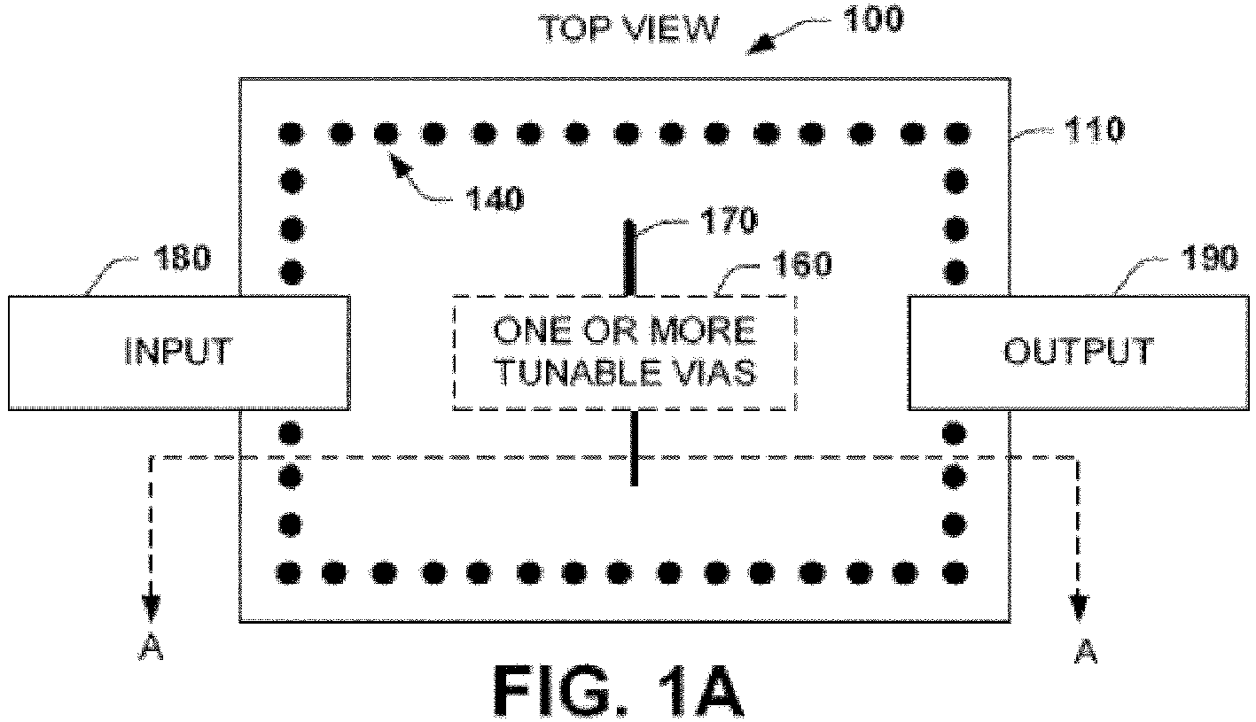
- FIG. 1A illustrates a top view 100 of an example integrated circuit waveguide apparatus 110 that employs a tunable material to provide a tunable filter.
- FIG. 1B illustrates a side view 120 of the apparatus 110 along the line A-A of the top view 100.
- the apparatus 110 includes a top conductive layer 130 for the integrated circuit waveguide filter.
- a bottom conductive layer 134 is on the other side of the integrated circuit waveguide filter.
- the top and bottom conductive layers 130 and 134 are coupled via a plurality of couplers (shown at reference numeral 140 of the top view and 140a of the bottom view) that form an outline of the waveguide filter.
- the couplers 140 can be conductive material such as copper or gold, for example, and can be configured to provide different waveguide filtering characteristics as is described below.
- a dielectric substrate layer 150 is disposed between the top conductive layer 130 and the bottom conductive layer 134 of the integrated circuit waveguide filter.
- the dielectric substrate layer 150 has a relative permittivity, ⁇ r that affects the tuning of the integrated circuit waveguide filter.
- At least one tunable via (reference numeral 160 for top view and 160a for side view) is provided and includes a tunable material that is disposed within the dielectric substrate layer 150 and is coupled to a set of electrodes 170.
- the set of electrodes 170 enable a voltage to be applied to the tunable material within the tunable via 160/160a to change the relative permittivity of the dielectric substrate layer 150 and to enable tuning the frequency characteristics of the integrated circuit waveguide filter.
- the apparatus 110 can include an input node 180 to receive an input signal and output node 190 to provide a filtered output signal such as a filter microwave signal, for example.
- the apparatus 110 can represent a single segment of a set of interconnected segments that collectively operate as a set of waveguides providing a collective filtering operation where each segment can be connected by a tunable iris segment.
- Various waveguide configurations can be provided that also employs the tunable materials described herein.
- SIW Substrate Integrated Waveguides
- RWG Ridged Waveguides
- Iris waveguides Iris-Coupled waveguides
- Post waveguides Post-wall waveguides
- Dual- or Multi-Mode waveguides Evanescent Mode waveguides
- Corrugated waveguides Waffle-Iron waveguides
- Absorptive waveguides Rectangular waveguides
- Circular waveguides for example.
- the tunable vias 160/160a can be provided as a single via that substantially fills the cavity of the dielectric substrate layer 150 in one example.
- the tunable vias 160/160a can be formed throughout the dielectric layer 150 (and or iris section as described below). When multiple vias 160/160a are employed, separate electrodes 170 would be attached to each of the separate vias respectively to enable tuning throughout the dielectric substrate layer 150.
- the tunable material can include BaSrTiO3 (BST) where, Ba is Barium, Sr is Strontium, and TiO3 is Titanate comprising Titanium and Oxygen.
- the BST is a piezoelectric material which allows for tuning described herein when a voltage is applied to the material.
- the BST has stable thermal properties in that it returns baseline properties (e.g., substantially no hysteresis) after heating or cooling above/below ambient temperatures.
- Other tunable materials can also be utilized where chemical formulas as altered to facilitate hysteresis stability.
- the tunable material in the vias 160/160a can include Ba x Ca 1-x TiO 3 , where Ca is Calcium and x is varied in a range from about 0.2 to about 0.8 to facilitate hysteresis stability of the tunable material.
- the tunable material in the vias 160/160a can include Pb x Zr 1-x TiO 3 , where Pb is Lead, Zr is Zirconium, and x is varied in a range from about 0.05 to about 0.4 to facilitate hysteresis stability of the tunable material.
- the tunable material can include (Bi 3x ,Zn 2-3x )(Zn x Nb 2-x ) (BZN), where Bi is Bismuth, Zn is Zinc, Nb is Niobium, and x is 1/2 or 2/3 to facilitate hysteresis stability of the tunable material.
- the tunable material can be selected from at least one of PbLaZrTiO 3 , PbTiO 3 , BaCaZrTiO 3 , NaNO 3 , KNbO 3 , LiNbO 3 , LiTaTiO 3 , PbNb 2 O 6 , PbTa 2 O 6 , KSr(NbO 3 ), NaBa 2 (NbO 3 ) 5 , KH 2 PO 4 , where La is Lanthanum, Na is sodium, N is Nitrogen, K is potassium, Li is lithium, Ta is tantalum, H is Hydrogen, and P is Phosphorus.
- metal oxides can be utilized as part of the tunable materials.
- the metal oxides in the tunable materials can be selected from at least one of Mg, Ca, Sr, Ba, Be, Ra, Li, Na, K, Rb, Cs, Fr, Ti, V, Cr, Mn, Zr, Nb, Mo, Hf, Ta, and W, where Mg is Magnesium, Be is Beryllium, Ra is Radium, Rb is Rubidium, Cs is Cesium, Fr is Francium, V is Vanadium, Cr is Chromium, Mn is Manganese, Mo is Molybdenum, Hf is Hafnium, and W is Tungsten.
- the tunable material includes metal oxides selected from at least one of Al, Si, Sn, Pb, Bi, Sc, Y, La, Ce, Pr, and Nd, where Al is Aluminum, Si is Silicon, Sn is Tin, Sc is Scandium, Y is Yttrium, Ce is Cerium, Pr is Praseodymium, and Nd is Neodymium.
- the tunable material includes metal oxides selected from at least one of Mg 2 SiO 4 , MgO, CaTiO 3 , MgZrSrTiO 6 , MgTiO 3 , MgAl 2 O 4 , WO 3 , SnTiO 4 , ZrTiO 4 , CaSiO 3 , CaSnO 3 , CaWO 4 , CaZrO 3 , MgTa 2 O 6 , MgZrO 3 , MnO 2 , PbO, Bi 2 O 3 , and La 2 O 3 .
- metal oxides selected from at least one of Mg 2 SiO 4 , MgO, CaTiO 3 , MgZrSrTiO 6 , MgTiO 3 , MgAl 2 O 4 , WO 3 , SnTiO 4 , ZrTiO 4 , CaSiO 3 , CaSnO 3 , CaWO 4 , CaZrO 3
- the plurality of couplers 140/140a can be conductive vias that are configured as a low pass filter waveguide, a high pass filter waveguide, a band pass filter waveguide, or a band reject filter waveguide, for example. Also, the plurality of couplers 140/140a can be configured to provide waveform shaping that includes at least one of a monotonic filter, an elliptic filter, and a hybrid filter, for example.
- FIG. 2 illustrates an example of a segmented integrated circuit waveguide circuit 200 that employs a tunable material within and/or between respective segments to provide a tunable filter circuit.
- the circuit 200 includes at least two segments of an integrated circuit waveguide filter where the segments are shown as SEG 1 through SEG S, with S being a positive integer.
- the segments are coupled by an iris, where one example iris is shown at 210.
- Each segment of the integrated circuit waveguide filter includes a top conductive layer for the respective segment of the integrated circuit waveguide filter and a bottom conductive layer for the respective segment of the integrated circuit waveguide filter.
- a side view is not shown illustrating the inner layers of each segment however each segment can be configured as illustrated with respect to FIG. 1B .
- the top and bottom conductive layers of the respective segment are coupled via a plurality of couplers that form an outline of the waveguide filter for the respective segment.
- One example set of couplers for a respective segment is shown at 220.
- a dielectric substrate layer is disposed between the top conductive layer and the bottom conductive layer of the respective segment of the integrated circuit waveguide filter.
- the dielectric substrate layer for the respective segment has a relative permittivity, ⁇ r that affects the tuning of the integrated circuit waveguide filter.
- At least one substrate tunable via includes a tunable material disposed within the dielectric substrate layer for the respective segment and is coupled to a set of electrodes.
- the substrate tunable vias are shown as STV1 through STVN, with N being a positive integer.
- a single tunable via can be provided per segment which substantially fills the dielectric material.
- each segment can have tunable vias disposed throughout the respective segment.
- a tunable area e.g., shape such as a rectangle that is larger than a via
- the set of electrodes for the tunable via in each segment enable a voltage to be applied to the tunable material within the tunable via to change the relative permittivity of the dielectric substrate layer for the respective segment and to enable tuning the frequency characteristics of the integrated circuit waveguide filter for the respective segment.
- at least one iris tunable via can be provided between segments that includes a tunable material disposed within the iris coupling the respective segments and is coupled, connected, and/or attached to a set of electrodes.
- An example iris tunable via is shown as 230.
- the set of electrodes for the iris tunable via enable a voltage to be applied to the tunable material within the tunable via of the iris to change the relative permittivity of the iris and to enable tuning the frequency characteristics of the integrated circuit waveguide filter.
- either iris tuning or cavity tuning may be applied.
- both iris tuning and cavity tuning can be applied to adjust the frequency characteristics of the integrated circuit waveguide filter.
- FIG. 3A illustrates an example of filter types that can be configured for an integrated circuit waveguide that employs a tunable material to provide a tunable filter.
- the filter types can be configured by how the couplers between the top and bottom layers are placed within a given segment of the waveguide.
- a low pass filter 300 can be configured where low frequencies are passed and higher frequencies are rejected.
- a high pass filter 310 can be configured where high frequencies are passed and lower frequencies are rejected by the waveguide.
- a band pass filter 330 can be configured where a range of selected frequencies within a given band of frequencies are passed and frequencies outside the band are rejected.
- a band reject filter 330 can be configured where selected frequencies within a given band are rejected and frequencies outside the given band are passed.
- FIG. 3B illustrates an example of a low pass filter configuration 340 that can be configured for an integrated circuit waveguide that employs a tunable material to provide a tunable filter.
- the low pass filter 340 is provided as an iris-coupled ridged waveguide but other configurations are possible as noted previously.
- FIG. 3C illustrates an example of a high pass filter configuration 350 that can be configured for an integrated circuit waveguide that employs a tunable material to provide a tunable filter.
- a substrate integrated waveguide is provided where couplers 360 between top and bottom planes of the waveguide are configured to provide a high pass filter function.
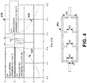
- FIG. 4 is an example of a monotonic filter configuration 400 and frequency diagram 410 for an integrated circuit waveguide that employs a tunable material to provide a tunable filter. As shown, rejection skirts at 420 and 430 in the diagram 410 for the monotonic filter 400 exhibit substantially no fly-back (e.g., no harmonic reentry).
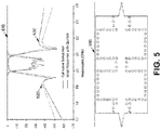
- FIG. 5 is an example of an elliptic filter configuration 500 and frequency diagram 510 for an integrated circuit waveguide that employs a tunable material to provide a tunable filter. As shown, rejection skirts at 520 and 530 in the diagram 510 for the elliptic filter 500 exhibit fly-back (e.g., harmonic reentry).
- fly-back e.g., harmonic reentry
- FIG. 6 is an example of a hybrid filter configuration 600 and frequency diagram 610 for an integrated circuit waveguide that employs a tunable material to provide a tunable filter.
- the hybrid filter 600 exhibits filter zeroes such as shown at 630.
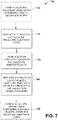
- FIG. 7 illustrates an example of a method 700 to fabricate an integrated circuit waveguide that employs a tunable material to provide a tunable filter.
- the method 700 includes forming a dielectric substrate layer of an integrated circuit waveguide filter (e.g., layer 150 of FIG. 1B ). Such forming can be depositing a silicon layer via chemical vapor deposition, for example.
- the dielectric substrate layer has a relative permittivity, ⁇ r that affects the tuning of the integrated circuit waveguide filter.
- the method 700 includes forming a top conductive layer on the dielectric substrate layer of the integrated circuit waveguide filter (e.g., layer 130 of FIG. 1B ).
- the method 700 includes forming a bottom conductive layer on the dielectric substrate layer of the integrated circuit waveguide filter (e.g., layer 134 of FIG. 1B ).
- the method includes depositing a plurality of couplers in the dielectric substrate layer to connect the top conductive layer and the bottom conductive layer (e.g., couplers 140/140a of FIG. 1A/1B ).
- the plurality of couplers form an outline of the waveguide filter and can define its respective filter capabilities.
- the method 750 includes forming at least one tunable area comprising a tunable material within the dielectric substrate layer (e.g., tunable vias 160/160a of FIG. 1A/1B ).
- the tunable area can be a via in one example or can be another shape such as a circle, ellipse, or rectangle that substantially fills the area within the outline of the waveguide filter formed by the respective couplers.
- the tunable area is coupled to a set of electrodes.
- the set of electrodes enable a voltage to be applied to the tunable material within the tunable area to change the relative permittivity of the dielectric substrate layer and to enable tuning the frequency characteristics of the integrated circuit waveguide filter.
- the method 700 can include forming the tunable material as BaSrTiO3 (or other materials and/or oxides) where, Ba is Barium, Sr is Strontium, and TiO3 is Titanate comprising Titanium and Oxygen.
Landscapes
- Engineering & Computer Science (AREA)
- Manufacturing & Machinery (AREA)
- Control Of Motors That Do Not Use Commutators (AREA)
Abstract
Description
- This disclosure relates to filter circuits, and more particularly to an integrated circuit waveguide that employs a tunable material to provide a tunable filter circuit.
- A waveguide filter is an electronic filter that is constructed with waveguide technology. Waveguides are typically hollow metal tubes inside which an electromagnetic wave may be transmitted. Filters are devices used to allow signals at some frequencies to pass (e.g., the passband), while others are rejected (e.g., the stopband). Filters are a basic component of electronic engineering circuits and have numerous applications. These include selection of signals and reduction of noise. Waveguide filters are most useful in the microwave band of frequencies, where they are a convenient size and have low loss. Examples of microwave filter use are found in satellite communications, telephone networks, and television broadcasting, for example. When employed as filters, air cavity waveguide filters have the ability to handle high power and low loss at a fixed frequency. To serve systems with multiple channels, several cavity filters are integrated with switches into a switched filter bank. With the addition of each channel however, the size increases, the cost increases and performance is lowered. These are three of the key performance distracters to air cavity waveguides. Another conventional waveguide filter is a Hititte tunable filter formed as a monolithic microwave integrated circuit (MMIC). This is a single MMIC with multiple tunable filter channels. While compact, these filters have very poor insertion loss (e.g., -30 to -8 dB) making them unusable for most filter bank applications.
- This disclosure relates an integrated circuit waveguide that employs a tunable material to provide a tunable filter circuit. In one aspect, an apparatus includes a top conductive layer of on an integrated circuit waveguide filter. The apparatus includes a bottom conductive layer of the integrated circuit waveguide filter. The top and bottom conductive layers are coupled via a plurality of couplers that form an outline of the waveguide filter. A dielectric substrate layer is disposed between the top conductive layer and the bottom conductive layer of the integrated circuit waveguide filter. The dielectric substrate layer has a relative permittivity, εr that affects the tuning of the integrated circuit waveguide filter. At least one tunable via comprising a tunable material is disposed within the dielectric substrate layer and is coupled to a set of electrodes. The set of electrodes enable a voltage to be applied to the tunable material within the tunable via to change the relative permittivity of the dielectric substrate layer and to enable tuning the frequency characteristics of the integrated circuit waveguide filter.
- In another aspect, a circuit includes at least two segments of an integrated circuit waveguide filter. The segments coupled by an iris. Each segment of the integrated circuit waveguide filter includes a top conductive layer for the respective segment of the integrated circuit waveguide filter and a bottom conductive layer for the respective segment of the integrated circuit waveguide filter. The top and bottom conductive layers of the respective segment are coupled via a plurality of couplers that form an outline of the waveguide filter for the respective segment. A dielectric substrate layer is disposed between the top conductive layer and the bottom conductive layer of the respective segment of the integrated circuit waveguide filter. The dielectric substrate layer for the respective segment has a relative permittivity, εr that affects the tuning of the integrated circuit waveguide filter. At least one substrate tunable via includes a tunable material disposed within the dielectric substrate layer for the respective segment and is coupled to a set of electrodes. The set of electrodes enable a voltage to be applied to the tunable material within the tunable via to change the relative permittivity of the dielectric substrate layer for the respective segment and to enable tuning the frequency characteristics of the integrated circuit waveguide filter for the respective segment. At least one iris tunable via includes a tunable material disposed within the iris coupling the respective segments and is coupled to a set of electrodes. The set of electrodes enable a voltage to be applied to the tunable material within the tunable via of the iris to change the relative permittivity of the iris and to enable tuning the frequency characteristics of the integrated circuit waveguide filter.
- In yet another aspect, a method includes forming a dielectric substrate layer of an integrated circuit waveguide filter. The dielectric substrate layer has a relative permittivity, εr that affects the tuning of the integrated circuit waveguide filter. The method includes forming a top conductive layer on the dielectric substrate layer of the integrated circuit waveguide filter. This includes forming a bottom conductive layer on the dielectric substrate layer of the integrated circuit waveguide filter. The method includes depositing a plurality of couplers in the dielectric substrate layer to connect the top conductive layer and the bottom conductive layer. The plurality of couplers form an outline of the waveguide filter. The method includes forming at least one tunable area comprising a tunable material within the dielectric substrate layer. The tunable area is coupled to a set of electrodes. The set of electrodes enable a voltage to be applied to the tunable material within the tunable area to change the relative permittivity of the dielectric substrate layer and to enable tuning the frequency characteristics of the integrated circuit waveguide filter.
-
-
FIG. 1A illustrates a top view of an example of an integrated circuit waveguide apparatus that employs a tunable material to provide a tunable filter. -
FIG. 1B illustrates a side view of an example of an integrated circuit waveguide apparatus that employs a tunable material to provide a tunable filter. -
FIG. 2 illustrates an example of a segmented integrated circuit waveguide circuit that employs a tunable material within and/or between respective segments to provide a tunable filter circuit. -
FIG. 3A illustrates an example of filter types that can be configured for an integrated circuit waveguide that employs a tunable material to provide a tunable filter. -
FIG. 3B illustrates an example of a low pass filter configuration that can be configured for an integrated circuit waveguide that employs a tunable material to provide a tunable filter. -
FIG. 3C illustrates an example of a high pass filter configuration that can be configured for an integrated circuit waveguide that employs a tunable material to provide a tunable filter. -
FIG. 4 is an example of a monotonic filter configuration and frequency diagram for an integrated circuit waveguide that employs a tunable material to provide a tunable filter. -
FIG. 5 is an example of an elliptic filter configuration and frequency diagram for an integrated circuit waveguide that employs a tunable material to provide a tunable filter. -
FIG. 6 is an example of a hybrid filter configuration and frequency diagram for an integrated circuit waveguide that employs a tunable material to provide a tunable filter. -
FIG. 7 illustrates an example of a method to fabricate an integrated circuit waveguide that employs a tunable material to provide a tunable filter. - This disclosure relates an integrated circuit waveguide that employs a tunable material to provide a tunable filter circuit. A substrate integrated waveguide (SIW) filter can be provided where a tunable material such as Barium (Ba) Strontium (Sr) Titanate (TiO3) (BST) (or other materials) can be embedded in a dielectric substrate layer of the waveguide (e.g., Silicon dielectric layer). The dielectric constant of the tunable material is changed by applying voltage, changing the effective dielectric constant of a dielectric loaded waveguide filter, thereby tuning the filter frequency. The tunable filter described herein can include an iris-connected SIW filter configuration that includes multiple filter segments, for example. This type of filter typically has three layers within each segment: a solid, bottom conductive plane; a solid, top conductive plane; and a middle dielectric plane having a dielectric constant insensitive to voltage. An iris can be disposed between cavities of the dielectric loaded waveguide filter, made by either cutting or etching out from the substrate or using vias to create an outline of the filter. Tuning capability is achieved by adding via holes into the dielectric filled cavities of the filter. These vias are then processed to add the tunable material such as BST. The top conductive plane can be fabricated such that voltage can be provided from a voltage source to each of the tunable material filled vias.
- When voltage is applied to the vias (or areas), the dielectric constant of the tunable material changes, which in turn changes the dielectric constant of the dielectric loaded waveguide filter, thereby achieving a tunable filter. By fabricating the vias throughout the filter cavities (or a single larger via in the cavity), the range of tuning can be increased. Further, by tuning the cavity vias and/or iris vias separately, the user can control the filters position in frequency as well as bandwidth. The resulting tunable filter is more compact, less expensive, and higher performance than a conventional switched filter bank that is tunable during operation. By eliminating switches and the need for multiple filters, a more selective and robust system is achieved.
-
FIG. 1A illustrates atop view 100 of an example integratedcircuit waveguide apparatus 110 that employs a tunable material to provide a tunable filter.FIG. 1B illustrates aside view 120 of theapparatus 110 along the line A-A of thetop view 100. As shown in theside view 120, theapparatus 110 includes a topconductive layer 130 for the integrated circuit waveguide filter. A bottomconductive layer 134 is on the other side of the integrated circuit waveguide filter. The top and bottomconductive layers reference numeral 140 of the top view and 140a of the bottom view) that form an outline of the waveguide filter. Thecouplers 140 can be conductive material such as copper or gold, for example, and can be configured to provide different waveguide filtering characteristics as is described below. - A
dielectric substrate layer 150 is disposed between the topconductive layer 130 and the bottomconductive layer 134 of the integrated circuit waveguide filter. Thedielectric substrate layer 150 has a relative permittivity, εr that affects the tuning of the integrated circuit waveguide filter. At least one tunable via (reference numeral 160 for top view and 160a for side view) is provided and includes a tunable material that is disposed within thedielectric substrate layer 150 and is coupled to a set ofelectrodes 170. The set ofelectrodes 170 enable a voltage to be applied to the tunable material within the tunable via 160/160a to change the relative permittivity of thedielectric substrate layer 150 and to enable tuning the frequency characteristics of the integrated circuit waveguide filter. As shown, theapparatus 110 can include aninput node 180 to receive an input signal andoutput node 190 to provide a filtered output signal such as a filter microwave signal, for example. - As will be illustrated and described below with respect to
FIG. 2 , theapparatus 110 can represent a single segment of a set of interconnected segments that collectively operate as a set of waveguides providing a collective filtering operation where each segment can be connected by a tunable iris segment. Various waveguide configurations can be provided that also employs the tunable materials described herein. These include Substrate Integrated Waveguides (SIW), Ridged Waveguides (RWG), Iris waveguides, Iris-Coupled waveguides, Post waveguides, Post-wall waveguides, Dual- or Multi-Mode waveguides, Evanescent Mode waveguides, Corrugated waveguides, Waffle-Iron waveguides, Absorptive waveguides, Rectangular waveguides, and Circular waveguides, for example. - The
tunable vias 160/160a can be provided as a single via that substantially fills the cavity of thedielectric substrate layer 150 in one example. In another example, thetunable vias 160/160a can be formed throughout the dielectric layer 150 (and or iris section as described below). Whenmultiple vias 160/160a are employed,separate electrodes 170 would be attached to each of the separate vias respectively to enable tuning throughout thedielectric substrate layer 150. In one example, the tunable material can include BaSrTiO3 (BST) where, Ba is Barium, Sr is Strontium, and TiO3 is Titanate comprising Titanium and Oxygen. - The BST is a piezoelectric material which allows for tuning described herein when a voltage is applied to the material. The BST has stable thermal properties in that it returns baseline properties (e.g., substantially no hysteresis) after heating or cooling above/below ambient temperatures. Other tunable materials can also be utilized where chemical formulas as altered to facilitate hysteresis stability. For example, the tunable material in the
vias 160/160a can include BaxCa1-xTiO3, where Ca is Calcium and x is varied in a range from about 0.2 to about 0.8 to facilitate hysteresis stability of the tunable material. - In another example, the tunable material in the
vias 160/160a can include PbxZr1-xTiO3, where Pb is Lead, Zr is Zirconium, and x is varied in a range from about 0.05 to about 0.4 to facilitate hysteresis stability of the tunable material. In yet another example, the tunable material can include (Bi3x,Zn2-3x)(ZnxNb2-x) (BZN), where Bi is Bismuth, Zn is Zinc, Nb is Niobium, and x is 1/2 or 2/3 to facilitate hysteresis stability of the tunable material. In still yet other examples, the tunable material can be selected from at least one of PbLaZrTiO3, PbTiO3, BaCaZrTiO3, NaNO3, KNbO3, LiNbO3, LiTaTiO3, PbNb2O6, PbTa2O6, KSr(NbO3), NaBa2(NbO3)5, KH2PO4, where La is Lanthanum, Na is sodium, N is Nitrogen, K is potassium, Li is lithium, Ta is tantalum, H is Hydrogen, and P is Phosphorus. - In some cases, metal oxides can be utilized as part of the tunable materials. The metal oxides in the tunable materials can be selected from at least one of Mg, Ca, Sr, Ba, Be, Ra, Li, Na, K, Rb, Cs, Fr, Ti, V, Cr, Mn, Zr, Nb, Mo, Hf, Ta, and W, where Mg is Magnesium, Be is Beryllium, Ra is Radium, Rb is Rubidium, Cs is Cesium, Fr is Francium, V is Vanadium, Cr is Chromium, Mn is Manganese, Mo is Molybdenum, Hf is Hafnium, and W is Tungsten. In another example, the tunable material includes metal oxides selected from at least one of Al, Si, Sn, Pb, Bi, Sc, Y, La, Ce, Pr, and Nd, where Al is Aluminum, Si is Silicon, Sn is Tin, Sc is Scandium, Y is Yttrium, Ce is Cerium, Pr is Praseodymium, and Nd is Neodymium. In other examples, the tunable material includes metal oxides selected from at least one of Mg2SiO4, MgO, CaTiO3, MgZrSrTiO6, MgTiO3, MgAl2O4, WO3, SnTiO4, ZrTiO4, CaSiO3, CaSnO3, CaWO4, CaZrO3, MgTa2O6, MgZrO3, MnO2, PbO, Bi2O3, and La2O3. As will be illustrated and described below with respect to
FIGS. 3 through 3B , the plurality ofcouplers 140/140a can be conductive vias that are configured as a low pass filter waveguide, a high pass filter waveguide, a band pass filter waveguide, or a band reject filter waveguide, for example. Also, the plurality ofcouplers 140/140a can be configured to provide waveform shaping that includes at least one of a monotonic filter, an elliptic filter, and a hybrid filter, for example. -
FIG. 2 illustrates an example of a segmented integratedcircuit waveguide circuit 200 that employs a tunable material within and/or between respective segments to provide a tunable filter circuit. Thecircuit 200 includes at least two segments of an integrated circuit waveguide filter where the segments are shown asSEG 1 through SEG S, with S being a positive integer. The segments are coupled by an iris, where one example iris is shown at 210. Each segment of the integrated circuit waveguide filter includes a top conductive layer for the respective segment of the integrated circuit waveguide filter and a bottom conductive layer for the respective segment of the integrated circuit waveguide filter. For purposes of brevity, a side view is not shown illustrating the inner layers of each segment however each segment can be configured as illustrated with respect toFIG. 1B . - The top and bottom conductive layers of the respective segment are coupled via a plurality of couplers that form an outline of the waveguide filter for the respective segment. One example set of couplers for a respective segment is shown at 220. A dielectric substrate layer is disposed between the top conductive layer and the bottom conductive layer of the respective segment of the integrated circuit waveguide filter. The dielectric substrate layer for the respective segment has a relative permittivity, εr that affects the tuning of the integrated circuit waveguide filter. At least one substrate tunable via includes a tunable material disposed within the dielectric substrate layer for the respective segment and is coupled to a set of electrodes. The substrate tunable vias are shown as STV1 through STVN, with N being a positive integer. As noted previously, a single tunable via can be provided per segment which substantially fills the dielectric material. In another example, each segment can have tunable vias disposed throughout the respective segment. In another example, a tunable area (e.g., shape such as a rectangle that is larger than a via) can be provided within the iris and/or waveguide segment.
- The set of electrodes for the tunable via in each segment enable a voltage to be applied to the tunable material within the tunable via to change the relative permittivity of the dielectric substrate layer for the respective segment and to enable tuning the frequency characteristics of the integrated circuit waveguide filter for the respective segment. In this example, at least one iris tunable via can be provided between segments that includes a tunable material disposed within the iris coupling the respective segments and is coupled, connected, and/or attached to a set of electrodes. An example iris tunable via is shown as 230. The set of electrodes for the iris tunable via enable a voltage to be applied to the tunable material within the tunable via of the iris to change the relative permittivity of the iris and to enable tuning the frequency characteristics of the integrated circuit waveguide filter. In some cases, either iris tuning or cavity tuning may be applied. In other examples, both iris tuning and cavity tuning can be applied to adjust the frequency characteristics of the integrated circuit waveguide filter.
-
FIG. 3A illustrates an example of filter types that can be configured for an integrated circuit waveguide that employs a tunable material to provide a tunable filter. As noted previously, the filter types can be configured by how the couplers between the top and bottom layers are placed within a given segment of the waveguide. In one example, alow pass filter 300 can be configured where low frequencies are passed and higher frequencies are rejected. In another example, ahigh pass filter 310 can be configured where high frequencies are passed and lower frequencies are rejected by the waveguide. In yet another example, aband pass filter 330 can be configured where a range of selected frequencies within a given band of frequencies are passed and frequencies outside the band are rejected. In still yet another example, aband reject filter 330 can be configured where selected frequencies within a given band are rejected and frequencies outside the given band are passed. -
FIG. 3B illustrates an example of a lowpass filter configuration 340 that can be configured for an integrated circuit waveguide that employs a tunable material to provide a tunable filter. In this example, thelow pass filter 340 is provided as an iris-coupled ridged waveguide but other configurations are possible as noted previously.FIG. 3C illustrates an example of a highpass filter configuration 350 that can be configured for an integrated circuit waveguide that employs a tunable material to provide a tunable filter. In this example, a substrate integrated waveguide is provided wherecouplers 360 between top and bottom planes of the waveguide are configured to provide a high pass filter function. -
FIG. 4 is an example of amonotonic filter configuration 400 and frequency diagram 410 for an integrated circuit waveguide that employs a tunable material to provide a tunable filter. As shown, rejection skirts at 420 and 430 in the diagram 410 for themonotonic filter 400 exhibit substantially no fly-back (e.g., no harmonic reentry). -
FIG. 5 is an example of anelliptic filter configuration 500 and frequency diagram 510 for an integrated circuit waveguide that employs a tunable material to provide a tunable filter. As shown, rejection skirts at 520 and 530 in the diagram 510 for theelliptic filter 500 exhibit fly-back (e.g., harmonic reentry). -
FIG. 6 is an example of ahybrid filter configuration 600 and frequency diagram 610 for an integrated circuit waveguide that employs a tunable material to provide a tunable filter. In this example, thehybrid filter 600 exhibits filter zeroes such as shown at 630. - In view of the foregoing structural and functional features described above, an example method will be better appreciated with reference to
FIG. 7 . While, for purposes of simplicity of explanation, the method is shown and described as executing serially, it is to be understood and appreciated that the method is not limited by the illustrated order, as parts of the method could occur in different orders and/or concurrently from that shown and described herein. -
FIG. 7 illustrates an example of amethod 700 to fabricate an integrated circuit waveguide that employs a tunable material to provide a tunable filter. At 710, themethod 700 includes forming a dielectric substrate layer of an integrated circuit waveguide filter (e.g.,layer 150 ofFIG. 1B ). Such forming can be depositing a silicon layer via chemical vapor deposition, for example. The dielectric substrate layer has a relative permittivity, εr that affects the tuning of the integrated circuit waveguide filter. At 720, themethod 700 includes forming a top conductive layer on the dielectric substrate layer of the integrated circuit waveguide filter (e.g.,layer 130 ofFIG. 1B ). This can include a chemical deposition process and include depositing conductive materials such as gold, copper, or silver, for example. At 730, themethod 700 includes forming a bottom conductive layer on the dielectric substrate layer of the integrated circuit waveguide filter (e.g.,layer 134 ofFIG. 1B ). - At 740, the method includes depositing a plurality of couplers in the dielectric substrate layer to connect the top conductive layer and the bottom conductive layer (e.g.,
couplers 140/140a ofFIG. 1A/1B ). The plurality of couplers form an outline of the waveguide filter and can define its respective filter capabilities. At 740, themethod 750 includes forming at least one tunable area comprising a tunable material within the dielectric substrate layer (e.g.,tunable vias 160/160a ofFIG. 1A/1B ). The tunable area can be a via in one example or can be another shape such as a circle, ellipse, or rectangle that substantially fills the area within the outline of the waveguide filter formed by the respective couplers. The tunable area is coupled to a set of electrodes. The set of electrodes enable a voltage to be applied to the tunable material within the tunable area to change the relative permittivity of the dielectric substrate layer and to enable tuning the frequency characteristics of the integrated circuit waveguide filter. Although not shown, themethod 700 can include forming the tunable material as BaSrTiO3 (or other materials and/or oxides) where, Ba is Barium, Sr is Strontium, and TiO3 is Titanate comprising Titanium and Oxygen. - What has been described above are examples. It is, of course, not possible to describe every conceivable combination of components or methodologies, but one of ordinary skill in the art will recognize that many further combinations and permutations are possible. Accordingly, the disclosure is intended to embrace all such alterations, modifications, and variations that fall within the scope of this application, including the appended claims. As used herein, the term "includes" means includes but not limited to, the term "including" means including but not limited to. The term "based on" means based at least in part on. Additionally, where the disclosure or claims recite "a," "an," "a first," or "another" element, or the equivalent thereof, it should be interpreted to include one or more than one such element, neither requiring nor excluding two or more such elements.
Claims (15)
- A waveguide circuit filter (200) comprising:at least two segments (SEG1, SEG2), each segment (SEG1, SEG2) comprising a top conductive layer (130), a bottom conductive layer (130) and a dielectric substrate layer (150) disposed between the top conductive layer (130) and the bottom conductive layer (150), the dielectric substrate layer (150) for a respective segment having a relative permittivity εr that affects a tuning of the waveguide circuit filter (200);at least one tunable via (160, 160a) comprising a tunable material disposed within the dielectric substrate layer (150) for the respective segment, the at least one tunable via (160, 160a) coupled to a first set of electrodes (170); andan iris to couple the at least two segments (SEG1, SEG2), the iris comprising at least one tunable via (230) having a tunable material disposed therein, the at least one tunable via (230) coupled to a second set of electrodes (170).
- The waveguide circuit filter (200) of claim 1, wherein the first set of electrodes (170) to enable a voltage to be applied to the tunable material of the at least one tunable via (160, 160a) to change the relative permittivity εr of the dielectric substrate layer (150).
- The waveguide circuit filter (200) of claim 2, wherein the first set of electrodes (170) enable tuning of frequency characteristics of the waveguide circuit filter (200).
- The waveguide circuit filter (200) of claim 1, wherein the second set of electrodes (170) to enable a voltage to be applied to the tunable material of the at least one tunable via (230) to change the relative permittivity εr of the iris.
- The waveguide circuit filter (200) of claim 4, wherein the second set of electrodes (170) enable tuning of frequency characteristics of the waveguide circuit filter (200).
- The waveguide circuit filter (200) of claim 1, wherein the second set of electrodes (170) correspond to the first set of electrodes (170).
- The waveguide circuit filter (200) of claim 6, wherein the first set of electrodes (170) enable tuning of frequency characteristics of the circuit waveguide filter (200).
- The waveguide circuit filter (200) of claim 1, wherein the top conductive layer (130) and the bottom conductive layer (150) of each segment (SEG1, SEG2) are coupled via a plurality of couplers (140, 140a) to form an outline of the waveguide filter for a respective segment (SEG1, SEG2).
- The waveguide circuit filter (200) of claim 8, wherein the plurality of couplers (140, 140a) are conductive vias that are configured as one of a low pass filter waveguide, a high pass filter waveguide, a bandpass filter waveguide, and a band reject filter waveguide.
- The waveguide circuit filter (200) of claim 1, wherein the tunable material of one of the at least one tunable via (160, 160a) and the at least one tunable via (230) comprises a chemical composition of BaSrTiO3 where, Ba is Barium, Sr is Strontium, and TiO3 is Titanate comprising Titanium and Oxygen.
- The waveguide circuit filter (200) of claim 1, wherein the tunable material of one of the at least one tunable via (160, 160a) and the at least one tunable via (230) comprises a chemical composition of BaxCa1-xTiO3, where Ca is Calcium and x is varied in a range from about 0.2 to about 0.8 to facilitate hysteresis stability of the tunable material.
- The waveguide circuit filter (200) of claim 1, wherein the tunable material of one of the at least one tunable via (160, 160a) and the at least one tunable via (230) comprises a chemical composition of PbxZr1-xTiO3, where Pb is Lead, Zr is Zirconium, and x is varied in a range from about 0.05 to about 0.4 to facilitate hysteresis stability of the tunable material.
- The waveguide circuit filter (200) of claim 1, wherein the tunable material of one of the at least one tunable via (160, 160a) and the at least one tunable via (230) comprises a chemical composition of (Bi3x,Zn2-3x)(ZnxNb2-x) (BZN) where Bi is Bismuth, Zn is Zinc, Nb is Niobium, and x is 1/2 or 2/3 to facilitate hysteresis stability of the tunable material.
- The waveguide circuit filter (200) of claim 1, wherein the tunable material of one of the at least one tunable via (160, 160a) and the at least one tunable via (230) comprises PbLaZrTiO3, PbTiO3, BaCaZrTiO3, NaNO3, KNbO3, LiNbO3, LiTaTiO3, PbNb2O6, PbTa2O6, KSr(NbO3), NaBa2(NbO3)5, KH2PO4, where La is Lanthanum, Na is sodium, N is Nitrogen, K is potassium, Li is lithium, Ta is tantalum, H is Hydrogen, and P is Phosphorus.
- The waveguide circuit filter (200) of claim 1, wherein the tunable material of one of the at least one tunable via (160, 160a) and the at least one tunable via (230) includes a metal oxide selected from a chemical composition of at least one of: Mg, Ca, Sr, Ba, Be, Ra, Li, Na, K, Rb, Cs, Fr, Ti, V, Cr, Mn, Zr, Nb, Mo, Hf, Ta, W, Al, Si, Sn, Pb, Bi, Sc, Y, La, Ce, Pr, Nd, Mg2SiO4, MgO, CaTiO3, MgZrSrTiO6, MgTiO3, MgAl2O4, W03, SnTiO4, ZrTiO4, CaSiO3, CaSnO3, CaWO4, CaZrO3, MgTa2O6, MgZrO3, MnO2, PbO, Bi2O3, and La2O3, where Mg is Magnesium, Be is Beryllium, Ra is Radium, Rb is Rubidium, Cs is Cesium, Fr is Francium, V is Vanadium, Cr is Chromium, Mn is Manganese, Mo is Molybdenum, Hf is Hafnium, W is Tungsten, Al is Aluminum, Si is Silicon, Sn is Tin, Sc is Scandium, Y is Yttrium, Ce is Cerium, Pr is Praseodymium, and Nd is Neodymium.
Applications Claiming Priority (2)
| Application Number | Priority Date | Filing Date | Title |
|---|---|---|---|
| US15/010,987 US10027005B2 (en) | 2016-01-29 | 2016-01-29 | Voltage controlled tunable filter |
| EP17151950.7A EP3200271B1 (en) | 2016-01-29 | 2017-01-18 | Voltage controlled tunable filter |
Related Parent Applications (2)
| Application Number | Title | Priority Date | Filing Date |
|---|---|---|---|
| EP17151950.7A Division-Into EP3200271B1 (en) | 2016-01-29 | 2017-01-18 | Voltage controlled tunable filter |
| EP17151950.7A Division EP3200271B1 (en) | 2016-01-29 | 2017-01-18 | Voltage controlled tunable filter |
Publications (2)
| Publication Number | Publication Date |
|---|---|
| EP3686989A1 true EP3686989A1 (en) | 2020-07-29 |
| EP3686989B1 EP3686989B1 (en) | 2022-10-26 |
Family
ID=57838273
Family Applications (2)
| Application Number | Title | Priority Date | Filing Date |
|---|---|---|---|
| EP17151950.7A Active EP3200271B1 (en) | 2016-01-29 | 2017-01-18 | Voltage controlled tunable filter |
| EP20157215.3A Active EP3686989B1 (en) | 2016-01-29 | 2017-01-18 | Voltage controlled tunable filter |
Family Applications Before (1)
| Application Number | Title | Priority Date | Filing Date |
|---|---|---|---|
| EP17151950.7A Active EP3200271B1 (en) | 2016-01-29 | 2017-01-18 | Voltage controlled tunable filter |
Country Status (2)
| Country | Link |
|---|---|
| US (2) | US10027005B2 (en) |
| EP (2) | EP3200271B1 (en) |
Families Citing this family (14)
| Publication number | Priority date | Publication date | Assignee | Title |
|---|---|---|---|---|
| US10027005B2 (en) * | 2016-01-29 | 2018-07-17 | Northrop Grumman Systems Corporation | Voltage controlled tunable filter |
| CN109802208A (en) * | 2019-03-11 | 2019-05-24 | 重庆邮电大学 | Substrate integral wave guide filter and preparation method thereof for millimetre-wave attenuator |
| CN110336107B (en) * | 2019-06-24 | 2021-08-17 | 成都频岢微电子有限公司 | Band-pass or band-stop reconfigurable HMSIW filter |
| CN110911789B (en) * | 2019-11-18 | 2021-02-05 | 电子科技大学 | Substrate integrated waveguide band-pass filter |
| US10892549B1 (en) | 2020-02-28 | 2021-01-12 | Northrop Grumman Systems Corporation | Phased-array antenna system |
| EP3879623B1 (en) * | 2020-03-11 | 2025-08-27 | Nokia Technologies Oy | Apparatus comprising a waveguide for radio frequency signals |
| CN111293390B (en) * | 2020-03-26 | 2024-08-16 | 成都频岢微电子有限公司 | UIR loaded three-order double-passband substrate integrated waveguide filter |
| EP3893326B1 (en) * | 2020-04-06 | 2026-02-18 | Nokia Technologies Oy | Apparatus comprising a waveguide for radio frequency signals |
| CN112563702B (en) * | 2020-11-17 | 2021-09-14 | 杭州电子科技大学 | Miniaturized dual-mode filter based on HMSIW cavity and zero point adjusting method |
| CN113488750B (en) * | 2021-06-09 | 2022-07-29 | 电子科技大学 | S21 transmission matrix adjustable broadband band elimination filter |
| CN113540731B (en) * | 2021-09-15 | 2021-11-23 | 成都威频科技有限公司 | YIG loading substrate integrated waveguide structure |
| CN114497933B (en) * | 2022-01-07 | 2023-04-25 | 哈尔滨工业大学 | Adjustable band-stop filter with plasma cladding double-tooth-shaped structure |
| WO2025111158A1 (en) * | 2023-11-22 | 2025-05-30 | KYOCERA AVX Components Corporation | Multilayer filter, multilayer filter assembly, and methods for forming a multilayer filter |
| US20260058349A1 (en) * | 2024-08-23 | 2026-02-26 | Northrop Grumman Systems Corporation | Dynamic ultra-selective waveguide filter assembly |
Citations (1)
| Publication number | Priority date | Publication date | Assignee | Title |
|---|---|---|---|---|
| US8665040B1 (en) * | 2010-03-09 | 2014-03-04 | Purdue Research Foundation | Field programmable filter array |
Family Cites Families (10)
| Publication number | Priority date | Publication date | Assignee | Title |
|---|---|---|---|---|
| US5459123A (en) | 1994-04-08 | 1995-10-17 | Das; Satyendranath | Ferroelectric electronically tunable filters |
| US5923229A (en) * | 1997-09-12 | 1999-07-13 | Wytec, Inc. | Simultaneous polarization and frequency filtering of transmitter and receiver signals in single antenna systems |
| AU2001255481A1 (en) | 2000-04-20 | 2001-11-07 | Paratek Microwave, Inc. | Waveguide-finline tunable phase shifter |
| US6864763B2 (en) | 2002-09-05 | 2005-03-08 | Spx Corporation | Tunable coupling iris and method |
| US20060006966A1 (en) | 2004-07-08 | 2006-01-12 | Qinghua Kang | Electronically tunable ridged waveguide cavity filter and method of manufacture therefore |
| US7728701B2 (en) | 2006-06-12 | 2010-06-01 | Regents Of The University Of California | Waveguide-based MEMS tunable filters and phase shifters |
| CA2629035A1 (en) * | 2008-03-27 | 2009-09-27 | Her Majesty The Queen In Right Of Canada, As Represented By The Minister Of Industry, Through The Communications Research Centre Canada | Waveguide filter with broad stopband based on sugstrate integrated waveguide scheme |
| US8508319B1 (en) | 2008-11-13 | 2013-08-13 | Far-Tech, Inc. | Rapidly tunable RF cavity |
| US9755286B2 (en) * | 2014-12-05 | 2017-09-05 | Huawei Technologies Co., Ltd. | System and method for variable microwave phase shifter |
| US10027005B2 (en) * | 2016-01-29 | 2018-07-17 | Northrop Grumman Systems Corporation | Voltage controlled tunable filter |
-
2016
- 2016-01-29 US US15/010,987 patent/US10027005B2/en active Active
-
2017
- 2017-01-18 EP EP17151950.7A patent/EP3200271B1/en active Active
- 2017-01-18 EP EP20157215.3A patent/EP3686989B1/en active Active
-
2018
- 2018-06-14 US US16/008,848 patent/US10340568B2/en active Active
Patent Citations (1)
| Publication number | Priority date | Publication date | Assignee | Title |
|---|---|---|---|---|
| US8665040B1 (en) * | 2010-03-09 | 2014-03-04 | Purdue Research Foundation | Field programmable filter array |
Non-Patent Citations (2)
| Title |
|---|
| ENTESARI KAMRAN ET AL: "Tunable SIW Structures: Antennas, VCOs, and Filters", IEEE MICROWAVE MAGAZINE, IEEESERVICE CENTER, PISCATAWAY, NJ, US, vol. 16, no. 5, 1 June 2015 (2015-06-01), pages 34 - 54, XP011580297, ISSN: 1527-3342, [retrieved on 20150506], DOI: 10.1109/MMM.2015.2408273 * |
| JOEL D BARRERA ET AL: "Analysis of a Variable SIW Resonator Enabled by Dielectric Material Perturbations and Applications", IEEE TRANSACTIONS ON MICROWAVE THEORY AND TECHNIQUES, IEEE SERVICE CENTER, PISCATAWAY, NJ, US, vol. 61, no. 1, 1 January 2013 (2013-01-01), pages 225 - 233, XP011488059, ISSN: 0018-9480, DOI: 10.1109/TMTT.2012.2226052 * |
Also Published As
| Publication number | Publication date |
|---|---|
| US10340568B2 (en) | 2019-07-02 |
| US10027005B2 (en) | 2018-07-17 |
| US20170222292A1 (en) | 2017-08-03 |
| EP3200271B1 (en) | 2020-05-06 |
| US20180301780A1 (en) | 2018-10-18 |
| EP3200271A1 (en) | 2017-08-02 |
| EP3686989B1 (en) | 2022-10-26 |
Similar Documents
| Publication | Publication Date | Title |
|---|---|---|
| US10340568B2 (en) | Voltage controlled tunable filter | |
| US6717491B2 (en) | Hairpin microstrip line electrically tunable filters | |
| US6686817B2 (en) | Electronic tunable filters with dielectric varactors | |
| Wersing | their Applications for Microwave Components,' | |
| US6492883B2 (en) | Method of channel frequency allocation for RF and microwave duplexers | |
| US6404614B1 (en) | Voltage tuned dielectric varactors with bottom electrodes | |
| US20060152304A1 (en) | Electrically tunable notch filters | |
| US20050206482A1 (en) | Electronically tunable switched-resonator filter bank | |
| US7236068B2 (en) | Electronically tunable combine filter with asymmetric response | |
| JP2005217852A (en) | Tunable filter | |
| US7808765B2 (en) | Varactors including interconnect layers | |
| US20140232482A1 (en) | Transmission line resonator, band-pass filter and branching filter | |
| US6724280B2 (en) | Tunable RF devices with metallized non-metallic bodies | |
| DE112004001996T5 (en) | Passband bandwidth control in decoupled stacked bulk acoustic resonator devices | |
| US20070007853A1 (en) | Apparatus and method capable of a high fundamental acoustic resonance frequency and a wide resonance-free frequency range | |
| US20060006966A1 (en) | Electronically tunable ridged waveguide cavity filter and method of manufacture therefore | |
| US7042316B2 (en) | Waveguide dielectric resonator electrically tunable filter | |
| US20050200427A1 (en) | Apparatus, system and method capable of radio frequency switching using tunable dielectric capacitors | |
| US7397329B2 (en) | Compact tunable filter and method of operation and manufacture therefore | |
| US20060033593A1 (en) | Method and apparatus with improved varactor quality factor | |
| CN112787616A (en) | Frequency modulation method of resonator |
Legal Events
| Date | Code | Title | Description |
|---|---|---|---|
| PUAI | Public reference made under article 153(3) epc to a published international application that has entered the european phase |
Free format text: ORIGINAL CODE: 0009012 |
|
| STAA | Information on the status of an ep patent application or granted ep patent |
Free format text: STATUS: THE APPLICATION HAS BEEN PUBLISHED |
|
| AC | Divisional application: reference to earlier application |
Ref document number: 3200271 Country of ref document: EP Kind code of ref document: P |
|
| AK | Designated contracting states |
Kind code of ref document: A1 Designated state(s): AL AT BE BG CH CY CZ DE DK EE ES FI FR GB GR HR HU IE IS IT LI LT LU LV MC MK MT NL NO PL PT RO RS SE SI SK SM TR |
|
| STAA | Information on the status of an ep patent application or granted ep patent |
Free format text: STATUS: REQUEST FOR EXAMINATION WAS MADE |
|
| 17P | Request for examination filed |
Effective date: 20210129 |
|
| RBV | Designated contracting states (corrected) |
Designated state(s): AL AT BE BG CH CY CZ DE DK EE ES FI FR GB GR HR HU IE IS IT LI LT LU LV MC MK MT NL NO PL PT RO RS SE SI SK SM TR |
|
| STAA | Information on the status of an ep patent application or granted ep patent |
Free format text: STATUS: EXAMINATION IS IN PROGRESS |
|
| 17Q | First examination report despatched |
Effective date: 20210430 |
|
| GRAP | Despatch of communication of intention to grant a patent |
Free format text: ORIGINAL CODE: EPIDOSNIGR1 |
|
| STAA | Information on the status of an ep patent application or granted ep patent |
Free format text: STATUS: GRANT OF PATENT IS INTENDED |
|
| GRAJ | Information related to disapproval of communication of intention to grant by the applicant or resumption of examination proceedings by the epo deleted |
Free format text: ORIGINAL CODE: EPIDOSDIGR1 |
|
| STAA | Information on the status of an ep patent application or granted ep patent |
Free format text: STATUS: EXAMINATION IS IN PROGRESS |
|
| INTG | Intention to grant announced |
Effective date: 20220525 |
|
| GRAP | Despatch of communication of intention to grant a patent |
Free format text: ORIGINAL CODE: EPIDOSNIGR1 |
|
| STAA | Information on the status of an ep patent application or granted ep patent |
Free format text: STATUS: GRANT OF PATENT IS INTENDED |
|
| INTC | Intention to grant announced (deleted) | ||
| INTG | Intention to grant announced |
Effective date: 20220719 |
|
| GRAS | Grant fee paid |
Free format text: ORIGINAL CODE: EPIDOSNIGR3 |
|
| GRAA | (expected) grant |
Free format text: ORIGINAL CODE: 0009210 |
|
| STAA | Information on the status of an ep patent application or granted ep patent |
Free format text: STATUS: THE PATENT HAS BEEN GRANTED |
|
| AC | Divisional application: reference to earlier application |
Ref document number: 3200271 Country of ref document: EP Kind code of ref document: P |
|
| AK | Designated contracting states |
Kind code of ref document: B1 Designated state(s): AL AT BE BG CH CY CZ DE DK EE ES FI FR GB GR HR HU IE IS IT LI LT LU LV MC MK MT NL NO PL PT RO RS SE SI SK SM TR |
|
| REG | Reference to a national code |
Ref country code: GB Ref legal event code: FG4D |
|
| REG | Reference to a national code |
Ref country code: CH Ref legal event code: EP |
|
| REG | Reference to a national code |
Ref country code: DE Ref legal event code: R096 Ref document number: 602017063175 Country of ref document: DE |
|
| REG | Reference to a national code |
Ref country code: AT Ref legal event code: REF Ref document number: 1527724 Country of ref document: AT Kind code of ref document: T Effective date: 20221115 |
|
| REG | Reference to a national code |
Ref country code: IE Ref legal event code: FG4D |
|
| REG | Reference to a national code |
Ref country code: NL Ref legal event code: FP |
|
| REG | Reference to a national code |
Ref country code: LT Ref legal event code: MG9D |
|
| REG | Reference to a national code |
Ref country code: AT Ref legal event code: MK05 Ref document number: 1527724 Country of ref document: AT Kind code of ref document: T Effective date: 20221026 |
|
| REG | Reference to a national code |
Ref country code: DE Ref legal event code: R082 Ref document number: 602017063175 Country of ref document: DE Representative=s name: FARAGO PATENTANWAELTE GMBH, DE |
|
| PG25 | Lapsed in a contracting state [announced via postgrant information from national office to epo] |
Ref country code: SE Free format text: LAPSE BECAUSE OF FAILURE TO SUBMIT A TRANSLATION OF THE DESCRIPTION OR TO PAY THE FEE WITHIN THE PRESCRIBED TIME-LIMIT Effective date: 20221026 Ref country code: PT Free format text: LAPSE BECAUSE OF FAILURE TO SUBMIT A TRANSLATION OF THE DESCRIPTION OR TO PAY THE FEE WITHIN THE PRESCRIBED TIME-LIMIT Effective date: 20230227 Ref country code: NO Free format text: LAPSE BECAUSE OF FAILURE TO SUBMIT A TRANSLATION OF THE DESCRIPTION OR TO PAY THE FEE WITHIN THE PRESCRIBED TIME-LIMIT Effective date: 20230126 Ref country code: LT Free format text: LAPSE BECAUSE OF FAILURE TO SUBMIT A TRANSLATION OF THE DESCRIPTION OR TO PAY THE FEE WITHIN THE PRESCRIBED TIME-LIMIT Effective date: 20221026 Ref country code: FI Free format text: LAPSE BECAUSE OF FAILURE TO SUBMIT A TRANSLATION OF THE DESCRIPTION OR TO PAY THE FEE WITHIN THE PRESCRIBED TIME-LIMIT Effective date: 20221026 Ref country code: ES Free format text: LAPSE BECAUSE OF FAILURE TO SUBMIT A TRANSLATION OF THE DESCRIPTION OR TO PAY THE FEE WITHIN THE PRESCRIBED TIME-LIMIT Effective date: 20221026 Ref country code: AT Free format text: LAPSE BECAUSE OF FAILURE TO SUBMIT A TRANSLATION OF THE DESCRIPTION OR TO PAY THE FEE WITHIN THE PRESCRIBED TIME-LIMIT Effective date: 20221026 |
|
| PG25 | Lapsed in a contracting state [announced via postgrant information from national office to epo] |
Ref country code: RS Free format text: LAPSE BECAUSE OF FAILURE TO SUBMIT A TRANSLATION OF THE DESCRIPTION OR TO PAY THE FEE WITHIN THE PRESCRIBED TIME-LIMIT Effective date: 20221026 Ref country code: PL Free format text: LAPSE BECAUSE OF FAILURE TO SUBMIT A TRANSLATION OF THE DESCRIPTION OR TO PAY THE FEE WITHIN THE PRESCRIBED TIME-LIMIT Effective date: 20221026 Ref country code: LV Free format text: LAPSE BECAUSE OF FAILURE TO SUBMIT A TRANSLATION OF THE DESCRIPTION OR TO PAY THE FEE WITHIN THE PRESCRIBED TIME-LIMIT Effective date: 20221026 Ref country code: IS Free format text: LAPSE BECAUSE OF FAILURE TO SUBMIT A TRANSLATION OF THE DESCRIPTION OR TO PAY THE FEE WITHIN THE PRESCRIBED TIME-LIMIT Effective date: 20230226 Ref country code: HR Free format text: LAPSE BECAUSE OF FAILURE TO SUBMIT A TRANSLATION OF THE DESCRIPTION OR TO PAY THE FEE WITHIN THE PRESCRIBED TIME-LIMIT Effective date: 20221026 Ref country code: GR Free format text: LAPSE BECAUSE OF FAILURE TO SUBMIT A TRANSLATION OF THE DESCRIPTION OR TO PAY THE FEE WITHIN THE PRESCRIBED TIME-LIMIT Effective date: 20230127 |
|
| P01 | Opt-out of the competence of the unified patent court (upc) registered |
Effective date: 20230607 |
|
| REG | Reference to a national code |
Ref country code: DE Ref legal event code: R097 Ref document number: 602017063175 Country of ref document: DE |
|
| PG25 | Lapsed in a contracting state [announced via postgrant information from national office to epo] |
Ref country code: SM Free format text: LAPSE BECAUSE OF FAILURE TO SUBMIT A TRANSLATION OF THE DESCRIPTION OR TO PAY THE FEE WITHIN THE PRESCRIBED TIME-LIMIT Effective date: 20221026 Ref country code: RO Free format text: LAPSE BECAUSE OF FAILURE TO SUBMIT A TRANSLATION OF THE DESCRIPTION OR TO PAY THE FEE WITHIN THE PRESCRIBED TIME-LIMIT Effective date: 20221026 Ref country code: EE Free format text: LAPSE BECAUSE OF FAILURE TO SUBMIT A TRANSLATION OF THE DESCRIPTION OR TO PAY THE FEE WITHIN THE PRESCRIBED TIME-LIMIT Effective date: 20221026 Ref country code: DK Free format text: LAPSE BECAUSE OF FAILURE TO SUBMIT A TRANSLATION OF THE DESCRIPTION OR TO PAY THE FEE WITHIN THE PRESCRIBED TIME-LIMIT Effective date: 20221026 Ref country code: CZ Free format text: LAPSE BECAUSE OF FAILURE TO SUBMIT A TRANSLATION OF THE DESCRIPTION OR TO PAY THE FEE WITHIN THE PRESCRIBED TIME-LIMIT Effective date: 20221026 |
|
| PG25 | Lapsed in a contracting state [announced via postgrant information from national office to epo] |
Ref country code: SK Free format text: LAPSE BECAUSE OF FAILURE TO SUBMIT A TRANSLATION OF THE DESCRIPTION OR TO PAY THE FEE WITHIN THE PRESCRIBED TIME-LIMIT Effective date: 20221026 Ref country code: AL Free format text: LAPSE BECAUSE OF FAILURE TO SUBMIT A TRANSLATION OF THE DESCRIPTION OR TO PAY THE FEE WITHIN THE PRESCRIBED TIME-LIMIT Effective date: 20221026 |
|
| REG | Reference to a national code |
Ref country code: CH Ref legal event code: PL |
|
| PLBE | No opposition filed within time limit |
Free format text: ORIGINAL CODE: 0009261 |
|
| STAA | Information on the status of an ep patent application or granted ep patent |
Free format text: STATUS: NO OPPOSITION FILED WITHIN TIME LIMIT |
|
| PG25 | Lapsed in a contracting state [announced via postgrant information from national office to epo] |
Ref country code: LU Free format text: LAPSE BECAUSE OF NON-PAYMENT OF DUE FEES Effective date: 20230118 |
|
| REG | Reference to a national code |
Ref country code: BE Ref legal event code: MM Effective date: 20230131 |
|
| 26N | No opposition filed |
Effective date: 20230727 |
|
| PG25 | Lapsed in a contracting state [announced via postgrant information from national office to epo] |
Ref country code: LI Free format text: LAPSE BECAUSE OF NON-PAYMENT OF DUE FEES Effective date: 20230131 Ref country code: CH Free format text: LAPSE BECAUSE OF NON-PAYMENT OF DUE FEES Effective date: 20230131 |
|
| PG25 | Lapsed in a contracting state [announced via postgrant information from national office to epo] |
Ref country code: SI Free format text: LAPSE BECAUSE OF FAILURE TO SUBMIT A TRANSLATION OF THE DESCRIPTION OR TO PAY THE FEE WITHIN THE PRESCRIBED TIME-LIMIT Effective date: 20221026 Ref country code: BE Free format text: LAPSE BECAUSE OF NON-PAYMENT OF DUE FEES Effective date: 20230131 |
|
| PG25 | Lapsed in a contracting state [announced via postgrant information from national office to epo] |
Ref country code: IE Free format text: LAPSE BECAUSE OF NON-PAYMENT OF DUE FEES Effective date: 20230118 |
|
| PG25 | Lapsed in a contracting state [announced via postgrant information from national office to epo] |
Ref country code: IT Free format text: LAPSE BECAUSE OF FAILURE TO SUBMIT A TRANSLATION OF THE DESCRIPTION OR TO PAY THE FEE WITHIN THE PRESCRIBED TIME-LIMIT Effective date: 20221026 |
|
| PG25 | Lapsed in a contracting state [announced via postgrant information from national office to epo] |
Ref country code: MC Free format text: LAPSE BECAUSE OF FAILURE TO SUBMIT A TRANSLATION OF THE DESCRIPTION OR TO PAY THE FEE WITHIN THE PRESCRIBED TIME-LIMIT Effective date: 20221026 |
|
| PG25 | Lapsed in a contracting state [announced via postgrant information from national office to epo] |
Ref country code: MC Free format text: LAPSE BECAUSE OF FAILURE TO SUBMIT A TRANSLATION OF THE DESCRIPTION OR TO PAY THE FEE WITHIN THE PRESCRIBED TIME-LIMIT Effective date: 20221026 |
|
| PG25 | Lapsed in a contracting state [announced via postgrant information from national office to epo] |
Ref country code: BG Free format text: LAPSE BECAUSE OF FAILURE TO SUBMIT A TRANSLATION OF THE DESCRIPTION OR TO PAY THE FEE WITHIN THE PRESCRIBED TIME-LIMIT Effective date: 20221026 |
|
| PG25 | Lapsed in a contracting state [announced via postgrant information from national office to epo] |
Ref country code: BG Free format text: LAPSE BECAUSE OF FAILURE TO SUBMIT A TRANSLATION OF THE DESCRIPTION OR TO PAY THE FEE WITHIN THE PRESCRIBED TIME-LIMIT Effective date: 20221026 |
|
| PGFP | Annual fee paid to national office [announced via postgrant information from national office to epo] |
Ref country code: DE Payment date: 20250121 Year of fee payment: 9 |
|
| PG25 | Lapsed in a contracting state [announced via postgrant information from national office to epo] |
Ref country code: CY Free format text: LAPSE BECAUSE OF FAILURE TO SUBMIT A TRANSLATION OF THE DESCRIPTION OR TO PAY THE FEE WITHIN THE PRESCRIBED TIME-LIMIT; INVALID AB INITIO Effective date: 20170118 |
|
| PG25 | Lapsed in a contracting state [announced via postgrant information from national office to epo] |
Ref country code: HU Free format text: LAPSE BECAUSE OF FAILURE TO SUBMIT A TRANSLATION OF THE DESCRIPTION OR TO PAY THE FEE WITHIN THE PRESCRIBED TIME-LIMIT; INVALID AB INITIO Effective date: 20170118 |
|
| PG25 | Lapsed in a contracting state [announced via postgrant information from national office to epo] |
Ref country code: TR Free format text: LAPSE BECAUSE OF FAILURE TO SUBMIT A TRANSLATION OF THE DESCRIPTION OR TO PAY THE FEE WITHIN THE PRESCRIBED TIME-LIMIT Effective date: 20221026 |
|
| PGFP | Annual fee paid to national office [announced via postgrant information from national office to epo] |
Ref country code: NL Payment date: 20260121 Year of fee payment: 10 |
|
| PGFP | Annual fee paid to national office [announced via postgrant information from national office to epo] |
Ref country code: GB Payment date: 20260123 Year of fee payment: 10 |
|
| PGFP | Annual fee paid to national office [announced via postgrant information from national office to epo] |
Ref country code: FR Payment date: 20260123 Year of fee payment: 10 |