EP3686953A1 - Battery pack - Google Patents
Battery pack Download PDFInfo
- Publication number
- EP3686953A1 EP3686953A1 EP19215104.1A EP19215104A EP3686953A1 EP 3686953 A1 EP3686953 A1 EP 3686953A1 EP 19215104 A EP19215104 A EP 19215104A EP 3686953 A1 EP3686953 A1 EP 3686953A1
- Authority
- EP
- European Patent Office
- Prior art keywords
- battery cells
- cell
- circuit board
- printed circuit
- battery
- Prior art date
- Legal status (The legal status is an assumption and is not a legal conclusion. Google has not performed a legal analysis and makes no representation as to the accuracy of the status listed.)
- Granted
Links
Images


Classifications
-
- H—ELECTRICITY
- H01—ELECTRIC ELEMENTS
- H01M—PROCESSES OR MEANS, e.g. BATTERIES, FOR THE DIRECT CONVERSION OF CHEMICAL ENERGY INTO ELECTRICAL ENERGY
- H01M50/00—Constructional details or processes of manufacture of the non-active parts of electrochemical cells other than fuel cells, e.g. hybrid cells
- H01M50/50—Current conducting connections for cells or batteries
- H01M50/572—Means for preventing undesired use or discharge
- H01M50/574—Devices or arrangements for the interruption of current
- H01M50/581—Devices or arrangements for the interruption of current in response to temperature
-
- H—ELECTRICITY
- H01—ELECTRIC ELEMENTS
- H01M—PROCESSES OR MEANS, e.g. BATTERIES, FOR THE DIRECT CONVERSION OF CHEMICAL ENERGY INTO ELECTRICAL ENERGY
- H01M10/00—Secondary cells; Manufacture thereof
- H01M10/42—Methods or arrangements for servicing or maintenance of secondary cells or secondary half-cells
- H01M10/425—Structural combination with electronic components, e.g. electronic circuits integrated to the outside of the casing
- H01M10/4257—Smart batteries, e.g. electronic circuits inside the housing of the cells or batteries
-
- H—ELECTRICITY
- H01—ELECTRIC ELEMENTS
- H01M—PROCESSES OR MEANS, e.g. BATTERIES, FOR THE DIRECT CONVERSION OF CHEMICAL ENERGY INTO ELECTRICAL ENERGY
- H01M50/00—Constructional details or processes of manufacture of the non-active parts of electrochemical cells other than fuel cells, e.g. hybrid cells
- H01M50/20—Mountings; Secondary casings or frames; Racks, modules or packs; Suspension devices; Shock absorbers; Transport or carrying devices; Holders
- H01M50/204—Racks, modules or packs for multiple batteries or multiple cells
- H01M50/207—Racks, modules or packs for multiple batteries or multiple cells characterised by their shape
- H01M50/213—Racks, modules or packs for multiple batteries or multiple cells characterised by their shape adapted for cells having curved cross-section, e.g. round or elliptic
-
- H—ELECTRICITY
- H01—ELECTRIC ELEMENTS
- H01M—PROCESSES OR MEANS, e.g. BATTERIES, FOR THE DIRECT CONVERSION OF CHEMICAL ENERGY INTO ELECTRICAL ENERGY
- H01M50/00—Constructional details or processes of manufacture of the non-active parts of electrochemical cells other than fuel cells, e.g. hybrid cells
- H01M50/20—Mountings; Secondary casings or frames; Racks, modules or packs; Suspension devices; Shock absorbers; Transport or carrying devices; Holders
- H01M50/233—Mountings; Secondary casings or frames; Racks, modules or packs; Suspension devices; Shock absorbers; Transport or carrying devices; Holders characterised by physical properties of casings or racks, e.g. dimensions
- H01M50/24—Mountings; Secondary casings or frames; Racks, modules or packs; Suspension devices; Shock absorbers; Transport or carrying devices; Holders characterised by physical properties of casings or racks, e.g. dimensions adapted for protecting batteries from their environment, e.g. from corrosion
-
- H—ELECTRICITY
- H01—ELECTRIC ELEMENTS
- H01M—PROCESSES OR MEANS, e.g. BATTERIES, FOR THE DIRECT CONVERSION OF CHEMICAL ENERGY INTO ELECTRICAL ENERGY
- H01M50/00—Constructional details or processes of manufacture of the non-active parts of electrochemical cells other than fuel cells, e.g. hybrid cells
- H01M50/20—Mountings; Secondary casings or frames; Racks, modules or packs; Suspension devices; Shock absorbers; Transport or carrying devices; Holders
- H01M50/244—Secondary casings; Racks; Suspension devices; Carrying devices; Holders characterised by their mounting method
-
- H—ELECTRICITY
- H01—ELECTRIC ELEMENTS
- H01M—PROCESSES OR MEANS, e.g. BATTERIES, FOR THE DIRECT CONVERSION OF CHEMICAL ENERGY INTO ELECTRICAL ENERGY
- H01M50/00—Constructional details or processes of manufacture of the non-active parts of electrochemical cells other than fuel cells, e.g. hybrid cells
- H01M50/20—Mountings; Secondary casings or frames; Racks, modules or packs; Suspension devices; Shock absorbers; Transport or carrying devices; Holders
- H01M50/262—Mountings; Secondary casings or frames; Racks, modules or packs; Suspension devices; Shock absorbers; Transport or carrying devices; Holders with fastening means, e.g. locks
- H01M50/264—Mountings; Secondary casings or frames; Racks, modules or packs; Suspension devices; Shock absorbers; Transport or carrying devices; Holders with fastening means, e.g. locks for cells or batteries, e.g. straps, tie rods or peripheral frames
-
- H—ELECTRICITY
- H01—ELECTRIC ELEMENTS
- H01M—PROCESSES OR MEANS, e.g. BATTERIES, FOR THE DIRECT CONVERSION OF CHEMICAL ENERGY INTO ELECTRICAL ENERGY
- H01M50/00—Constructional details or processes of manufacture of the non-active parts of electrochemical cells other than fuel cells, e.g. hybrid cells
- H01M50/20—Mountings; Secondary casings or frames; Racks, modules or packs; Suspension devices; Shock absorbers; Transport or carrying devices; Holders
- H01M50/284—Mountings; Secondary casings or frames; Racks, modules or packs; Suspension devices; Shock absorbers; Transport or carrying devices; Holders with incorporated circuit boards, e.g. printed circuit boards [PCB]
-
- H—ELECTRICITY
- H01—ELECTRIC ELEMENTS
- H01M—PROCESSES OR MEANS, e.g. BATTERIES, FOR THE DIRECT CONVERSION OF CHEMICAL ENERGY INTO ELECTRICAL ENERGY
- H01M50/00—Constructional details or processes of manufacture of the non-active parts of electrochemical cells other than fuel cells, e.g. hybrid cells
- H01M50/50—Current conducting connections for cells or batteries
- H01M50/502—Interconnectors for connecting terminals of adjacent batteries; Interconnectors for connecting cells outside a battery casing
- H01M50/505—Interconnectors for connecting terminals of adjacent batteries; Interconnectors for connecting cells outside a battery casing comprising a single busbar
-
- H—ELECTRICITY
- H01—ELECTRIC ELEMENTS
- H01M—PROCESSES OR MEANS, e.g. BATTERIES, FOR THE DIRECT CONVERSION OF CHEMICAL ENERGY INTO ELECTRICAL ENERGY
- H01M50/00—Constructional details or processes of manufacture of the non-active parts of electrochemical cells other than fuel cells, e.g. hybrid cells
- H01M50/50—Current conducting connections for cells or batteries
- H01M50/502—Interconnectors for connecting terminals of adjacent batteries; Interconnectors for connecting cells outside a battery casing
- H01M50/519—Interconnectors for connecting terminals of adjacent batteries; Interconnectors for connecting cells outside a battery casing comprising printed circuit boards [PCB]
-
- H—ELECTRICITY
- H01—ELECTRIC ELEMENTS
- H01M—PROCESSES OR MEANS, e.g. BATTERIES, FOR THE DIRECT CONVERSION OF CHEMICAL ENERGY INTO ELECTRICAL ENERGY
- H01M50/00—Constructional details or processes of manufacture of the non-active parts of electrochemical cells other than fuel cells, e.g. hybrid cells
- H01M50/50—Current conducting connections for cells or batteries
- H01M50/569—Constructional details of current conducting connections for detecting conditions inside cells or batteries, e.g. details of voltage sensing terminals
-
- H—ELECTRICITY
- H01—ELECTRIC ELEMENTS
- H01M—PROCESSES OR MEANS, e.g. BATTERIES, FOR THE DIRECT CONVERSION OF CHEMICAL ENERGY INTO ELECTRICAL ENERGY
- H01M10/00—Secondary cells; Manufacture thereof
- H01M10/42—Methods or arrangements for servicing or maintenance of secondary cells or secondary half-cells
- H01M10/48—Accumulators combined with arrangements for measuring, testing or indicating the condition of cells, e.g. the level or density of the electrolyte
- H01M10/482—Accumulators combined with arrangements for measuring, testing or indicating the condition of cells, e.g. the level or density of the electrolyte for several batteries or cells simultaneously or sequentially
-
- H—ELECTRICITY
- H01—ELECTRIC ELEMENTS
- H01M—PROCESSES OR MEANS, e.g. BATTERIES, FOR THE DIRECT CONVERSION OF CHEMICAL ENERGY INTO ELECTRICAL ENERGY
- H01M10/00—Secondary cells; Manufacture thereof
- H01M10/42—Methods or arrangements for servicing or maintenance of secondary cells or secondary half-cells
- H01M10/425—Structural combination with electronic components, e.g. electronic circuits integrated to the outside of the casing
- H01M2010/4271—Battery management systems including electronic circuits, e.g. control of current or voltage to keep battery in healthy state, cell balancing
-
- H—ELECTRICITY
- H01—ELECTRIC ELEMENTS
- H01M—PROCESSES OR MEANS, e.g. BATTERIES, FOR THE DIRECT CONVERSION OF CHEMICAL ENERGY INTO ELECTRICAL ENERGY
- H01M2200/00—Safety devices for primary or secondary batteries
-
- H—ELECTRICITY
- H01—ELECTRIC ELEMENTS
- H01M—PROCESSES OR MEANS, e.g. BATTERIES, FOR THE DIRECT CONVERSION OF CHEMICAL ENERGY INTO ELECTRICAL ENERGY
- H01M2200/00—Safety devices for primary or secondary batteries
- H01M2200/10—Temperature sensitive devices
- H01M2200/103—Fuse
-
- Y—GENERAL TAGGING OF NEW TECHNOLOGICAL DEVELOPMENTS; GENERAL TAGGING OF CROSS-SECTIONAL TECHNOLOGIES SPANNING OVER SEVERAL SECTIONS OF THE IPC; TECHNICAL SUBJECTS COVERED BY FORMER USPC CROSS-REFERENCE ART COLLECTIONS [XRACs] AND DIGESTS
- Y02—TECHNOLOGIES OR APPLICATIONS FOR MITIGATION OR ADAPTATION AGAINST CLIMATE CHANGE
- Y02E—REDUCTION OF GREENHOUSE GAS [GHG] EMISSIONS, RELATED TO ENERGY GENERATION, TRANSMISSION OR DISTRIBUTION
- Y02E60/00—Enabling technologies; Technologies with a potential or indirect contribution to GHG emissions mitigation
- Y02E60/10—Energy storage using batteries
Definitions
- Embodiments relate to a battery pack.
- An electronic device e.g., a notebook computer, a mini notebook computer, a net-book, a mobile computer, an ultra-mobile personal computer (UMPC) or a portable multimedia player (PMP), may use a battery pack in which a plurality of batteries connected in series and/or parallel as a portable power supply.
- UMPC ultra-mobile personal computer
- PMP portable multimedia player
- the battery pack may include a protective circuit module (PCM) for protecting battery cells from over-charge, over-discharge, and/or over-current, and multiple battery cells and the PCM may be housed together in a case.
- PCM protective circuit module
- the embodiments may be realized by providing a battery pack including a plurality of battery cells, each battery cell having a positive electrode and a negative electrode on a top surface of the battery cell, the plurality of battery cells being arranged in a first direction and in a second direction crossing the first direction; a protective circuit module, the protective circuit module including a printed circuit board on the plurality of battery cells, and a plurality of conductive tabs on the printed circuit board and electrically connecting the plurality of battery cells; and a case accommodating the plurality of battery cells and the protective circuit module, wherein each of the conductive tabs include a substrate connector connected to the printed circuit board, a cell connector electrically connected to a battery cell of the plurality of battery cells, and a fusible link extending from the substrate connector and having a width that is smaller than that of the substrate connector.
- the substrate connector may include a first electrode substrate connector connected to the cell connector and a second electrode substrate connector spaced a predetermined distance apart from the first electrode substrate connector on the same plane, and the fusible link may connect the first electrode substrate connector with the second electrode substrate connector and is bent to then detour at least one times on a plane.
- the fusible link may be in contact with the printed circuit board.
- the fusible link may be spaced apart from a top surface of the printed circuit board in a third direction crossing the first direction and the second direction.
- the battery pack may further include a flame-retardant coating between the top surface of the printed circuit board and the fusible link.
- the cell connector may be lower than the substrate connector and may include at least one stepped portion connecting the cell connector with the substrate connector.
- the conductive tabs may include a plurality of connection tabs connecting a row of neighboring battery cells in the second direction; a plurality of positive cell tabs electrically connected to a first column of battery cells at a first side of the plurality of battery cells, the first column of battery cells being arranged in the first direction; and a plurality of negative cell tabs electrically connected to a second column of battery cells at a second side of the plurality of battery cells, the second column of battery cells being arranged in the first direction.
- the plurality of connection tabs, the plurality of positive cell tabs, and the plurality of negative cell tabs may be on a top surface of the printed circuit board.
- the printed circuit board may include a plurality of throughholes passing therethrough, the plurality of throughholes being aligned with tops of the plurality of battery cells, and the plurality of connection tabs, the plurality of positive cell tabs, and the plurality of negative cell tabs may pass through the throughholes and are electrically connected to the plurality of battery cells, respectively.
- the battery pack may further include a holder, the holder including a plurality of receivers arranged in the first direction and the second direction, the plurality of receivers passing through the holder, accommodating the plurality of battery cells in the receivers, and having the protective circuit module thereon; and bus bars in the holder, the bus bars including a positive bus bar electrically connected to the plurality of positive cell tabs through the printed circuit board, and a negative bus bar electrically connected to the plurality of negative cell tabs through the printed circuit board.
- the battery pack may further include a fuse in the negative bus bar, the fuse being cut off when an internal short circuit or an external short circuit is generated in the battery pack.
- the embodiments may be realized by providing a battery pack including a plurality of battery cells, each battery cell having a positive electrode and a negative electrode on a top surface of the battery cell, the plurality of battery cells being arranged in a row direction and in a column direction crossing the row direction; a protective circuit module, the protective circuit module including a printed circuit board on the plurality of battery cells, and a plurality of conductive tabs on the printed circuit board and electrically connecting the plurality of battery cells; and a case accommodating the plurality of battery cells and the protective circuit module, wherein the plurality of conductive tabs include a plurality of connection tabs electrically connecting a row of neighboring battery cells in the row direction; a plurality of positive cell tabs electrically connected to a first column of battery cells at a first side of the plurality of battery cells, the first column of battery cells being arranged in the column direction; and a plurality of negative cell tabs electrically connected to a second column of battery cells at a second side of the plurality of battery cells, the second
- the embodiments may be realized by providing a battery pack in which a plurality of battery cells are accommodatable, each battery cell having a positive electrode and a negative electrode on a top surface thereof and the plurality of battery cells being arrangeable in a row direction and in a column direction crossing the row direction, the battery pack including a protective circuit module, the protective circuit module including a printed circuit board to cover the plurality of battery cells, and a plurality of conductive tabs on the printed circuit board to electrically connect the plurality of battery cells; and a case to accommodate the plurality of battery cells and the protective circuit module, wherein each of the conductive tabs include a substrate connector connected to the printed circuit board, a cell connector to electrically connect to a battery cell of the plurality of battery cells, and a fusible link extending from the substrate connector and having a width that is smaller than that of the substrate connector.
- first, second, etc. may be used herein to describe various members, elements, regions, layers and/or sections, these members, elements, regions, layers and/or sections should not be limited by these terms. These terms are only used to distinguish one member, element, region, layer and/or section from another. Thus, for example, a first member, a first element, a first region, a first layer and/or a first section discussed below could be termed a second member, a second element, a second region, a second layer and/or a second section without departing from the teachings of the present disclosure.
- spatially relative terms such as “below,” “beneath,” “lower,” “above,” “upper,” and the like, may be used herein for ease of description to describe one element or feature's relationship to another element(s) or feature(s) as illustrated in the figures. It will be understood that the spatially relative terms are intended to encompass different orientations of the device in use or operation in addition to the orientation depicted in the figures. For example, if the device in the figures is turned over, elements described as “below” or “beneath” other elements or features would then be oriented “on” or “above” the other elements or features. Thus, the exemplary term “below” can encompass both an orientation of above and below.
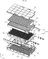
- FIGS. 1A and 1B illustrate a perspective view and an exploded perspective view illustrating a battery pack according to an embodiment.
- the battery pack 10 may include or accommodate a plurality of battery cells 100, a holder 200 (fixing the plurality of battery cells 100), a protective circuit module (PCM) 300 including a plurality of conductive tabs (320, 330 and 340 of FIGS. 4A to 4C ) electrically connected to the plurality of battery cells 100, bus bars 400 electrically connected or connectable to the plurality of battery cells 100, and a case 500 accommodating the plurality of battery cells 100, the holder 200, the PCM 300 and the bus bars 400.
- the battery pack 10 may be a high-capacity battery mounted in an electric vehicle.
- the plurality of battery cells 100 may be secondary batteries that supply an external electronic device with power and are rechargeable.
- the battery cells 100 may be, e.g., lithium polymer cells, lithium polymer ion cells, lithium ion cells, zinc air cells, lithium sulfur cells, lithium air cells, sodium ion cells, magnesium cells, or all-solid cells.
- the plurality of battery cells 100 may be cylindrical battery cells.
- the plurality of battery cells 100 may be, e.g., pouch battery cells or prismatic battery cells.
- the plurality of battery cells 100 may be battery cells having the same shape. For brevity, the following description will be made with regard to a case where the plurality of battery cells 100 are cylindrical battery cells.
- the battery cells 100 may be cylindrical battery cells extending in a third direction (y), which is a lengthwise direction of each battery cell, and each of the battery cells 100 may include both electrodes 110 and 120 (having different polarities) at a same end in the y direction (e.g., at its top end or bottom end).
- the battery cell 100 may include an electrode assembly accommodated in a cylindrical case having a top opening, and a cap plate sealing the top opening of the case.
- the positive electrode 110 may be at a center of the top end of the case, where the cap plate is positioned, and the negative electrode 120 may be at a crimping region of the case, upwardly extending to cover the edge part of the cap plate.
- the cap plate may function as a positive electrode
- the case may function as a negative electrode.
- the positive electrode 110 and the negative electrode 120 may be positioned at the top end of the battery cell 100 so as to be spaced apart from each other.
- the holder 200 may have a substantially hexahedron shape having a plurality of receivers 210 passing through or between its top and bottom surfaces to allow the plurality of battery cells 100 to be placed therein.
- FIG. 3 a perspective view, illustrating the connection relationship among the holder 200, the PCM 300, and the bus bar 400, is illustrated.
- configurations of the holder 200, the PCM 300, and the bus bars 400 will be described with reference to FIGS. 1B and 3 .
- the holder 200 may include ribs 220 partitioning the plurality of receivers 210, and the plurality of battery cells 100 may be accommodated in the plurality of receivers 210, respectively.
- the plurality of receivers 210 of the holder 200 may have shapes corresponding to those the plurality of battery cells 100. For example, if the plurality of battery cells 100 are cylindrical battery cells, the plurality of receivers 210 may also be cylindrical.
- the plurality of battery cells 100 may be inserted into the plurality of receivers 210 in a lengthwise direction.
- the holder 200 may include the plurality of receivers 210 regularly arranged in row and column directions parallel with side surfaces of the holder 200.
- the row direction in which the plurality of receivers 210 are arranged in the holder 200 may be a second direction (z) perpendicular to the third direction (y), which is parallel with a first side surface of the holder 200.
- the column direction in which the plurality of receiving units 210 are arranged may be perpendicular to the third direction (y) and the second direction (z), and may be a first direction (x), which is parallel with the second side surface of the holder 200.
- the first direction (x) may be a lengthwise (e.g., longer side) direction of the holder 200
- the second direction (z) may be a widthwise (e.g., shorter side) direction of the holder 200.
- the plurality of battery cells 100 may be accommodated in the plurality of receivers 210 of the holder 200 and may be regularly arranged in the first direction (x) and the second direction (z) in a state in which they are isolated by the ribs 220.
- top ends of the plurality of battery cells 100 may be exposed to an upper portion of the holder 200, and bottom ends thereof may be exposed to a lower portion of the holder 200.
- the positive electrode 110 and the negative electrode 120 may be positioned at the top end of each of the plurality of battery cells 100.
- the battery cells 100 arranged on or along the same line in the second direction (z), which is the widthwise direction of the holder 200, may be regarded as one of a plurality of battery groups 101.
- the plurality of battery cells 100 may include the plurality of battery groups 101 arranged in or along the first direction (x), which is the lengthwise direction of the holder 200.
- the PCM 300 may be on the top surface of the holder 200.
- the PCM 300 may include a printed circuit board 310 having a plurality of circuit devices mounted thereon, and a plurality of conductive tabs 320, 330 and 340 for electrically connecting the plurality of battery cells 100.
- the plurality of conductive tabs 320, 330 and 340 may include positive cell tabs 320, negative cell tabs 330, and connection tabs 340, which may be all mounted on the top surface of the printed circuit board 310 to electrically connect the plurality of battery cells 100.
- FIGS. 4A , 4B and 4C enlarged views of portions 4a, 4b, and 4c in FIG. 3 are illustrated.
- FIGS. 5A, 5B and 5C perspective views of a positive cell tab 320, a negative cell tab 330, and a connection tab 340 shown in FIG. 3 are illustrated.
- the PCM 300 will be described with reference to FIGS. 4A , 4B , 4C , 5A , 5B and 5C .
- the printed circuit board 310 may include throughholes 311 passing therethrough, e.g., between its top and bottom surfaces.
- the plurality of throughholes may be at regions corresponding to, overlying, or aligned with top portions of the plurality of battery cells 100.
- the printed circuit board 310 may include an substantially planar insulation layer, a plurality of circuit patterns, and a plurality of connection pads, which are electrically disconnected or isolated by the insulation layer.
- the connection pads may be portions of the printed circuit board 310, which are electrically connected to the plurality of conductive tabs 320, 330 and 340 and circuit devices.
- the plurality of circuit patterns may electrically connect the plurality of connection pads in the insulation layer.
- the PCM 300 may further include circuit devices (e.g., a plurality of voltage sensors) mounted on the connection pads of the printed circuit board 310.
- the PCM 300 may basically protect the plurality of battery cells 110 by preventing the plurality of battery cells 110 from being over-discharged and/or overcharged or by preventing over-current from flowing through the plurality of battery cells 110.
- the plurality of conductive tabs 320, 330, and 340 may be mounted on the connection pads on the top surface of the printed circuit board 310, thereby electrically connecting the plurality of conductive tabs 320, 330, and 340 to the printed circuit board 310.
- the plurality of conductive tabs 320, 330, and 340 may be electrically connected to the plurality of battery cells 100 through the throughholes 311 in the printed circuit board 310, respectively.
- the positive electrodes 110 and the negative electrodes 120 of the plurality of battery cells 100 may be positioned lower than the top surface of the printed circuit board 310 in the third direction (y).
- the plurality of conductive tabs 320, 330, and 340 may include positive cell tabs 320, negative cell tabs 330, and connection tabs 340.
- each of the positive cell tabs 320, the negative cell tabs 330, and the connection tabs 340 may be one-body, monolithic metal tabs.
- the positive cell tabs 320 may be in the throughholes 311 arranged in the first direction (x) at or adjacent to a first side 310a of the top surface of the printed circuit board 310.
- the positive cell tabs 320 may be electrically connected to (e.g., positive electrodes 110 of) the battery cells among the plurality of battery cells 100, at one-side end and arranged in the first direction (x), which is a column direction, respectively.
- the positive cell tabs 320 may be electrically connected to a positive electrode bus bar 410 along a first side of the second side surface of the holder 200 through the printed circuit board 310.
- the negative cell tabs 330 may be in the throughholes 311 arranged in the first direction (x) at or adjacent to a second side 310b of the top surface of the printed circuit board 310, the second side 310b being spaced from the first side 310a along the second direction (z).
- the negative cell tabs 330 may be electrically connected to (e.g., negative electrodes 120 of) the battery cells among the plurality of battery cells 100, positioned at the second side and arranged in the first direction (x), which is a column direction, respectively.
- the negative cell tabs 330 may be electrically connected to a negative electrode bus bar 420 along a second side of the second side surface of the holder 200 through the printed circuit board 310.
- the positive cell tab 320 may include a first positive electrode substrate connector 321, a second positive electrode substrate connector 322, a first positive cell connector 323, a positive electrode fusible link 324, and a positive electrode stepped portion 325.
- the first positive electrode substrate connector 321 and the second positive electrode substrate connector 322 may have substantially planar plate shapes, and may be electrically and mechanically connected to connection pads on the top surface of the printed circuit board 310.
- the connection pads may be electrically connected to voltage sensors through the circuit patterns on the printed circuit board 310.
- the voltage sensors of the printed circuit board 310 may measure voltages of the battery cells 100 electrically connected to the positive cell tabs 320.
- the first positive electrode substrate connector 321 and the second positive electrode substrate connector 322 may be on the same plane and may be spaced a predetermined distance apart from each other.
- the plane may be defined by the first direction (x) and the second direction (z) perpendicular to each other.
- Each of the first positive electrode substrate connector 321 and the second positive electrode substrate connector 322 may include at least one soldering hole 321a, 322a passing therethrough, e.g., between top and bottom surfaces.
- solder may be melted and filled in the soldering holes 321a and 322a in a state in which first positive electrode substrate connector 321 and the second positive electrode substrate connector 322 of the positive cell tab 320 are mounted on the top surface of the connection pad of the printed circuit board 310, thereby electrically connecting the positive cell tab 320 and the printed circuit board 310.
- the first positive electrode substrate connector 321 and the second positive electrode substrate connector 322 may be mounted on the connection pads on the printed circuit board 310.
- the first positive electrode substrate connector 321 and the second positive electrode substrate connector 322 may further include position determining protrusions 321b and 322b, which downwardly protrude (e.g., into the PCM 300), respectively.
- the position determining protrusions 321b and 322b may be inserted into position determining holes 312 in the printed circuit board 310 to determine positions of the printed circuit board 310, where the positive cell tabs 320 are fixed and coupled.
- the first positive electrode substrate connector 321 and the second positive electrode substrate connector 322 may help prevent the positive cell tabs 320 from deviating from the printed circuit board 310 by the position determining protrusions 321b and 322b.
- the second positive electrode substrate connector 322 may be electrically connected to the bus bars 400 through the printed circuit board 310.
- the first positive electrode substrate connector 321 may be electrically connected to the connection pad of the printed circuit board 310 and may be electrically connected to the first positive cell connector 323 through the positive electrode stepped portion 325.
- the first positive cell connector 323 may be electrically connected to the printed circuit board 310 through the positive electrode stepped portion 325 and the first positive electrode substrate connector 321.
- the first positive cell connector 323 may be a region electrically connected to the positive electrode 110 at the top end of the battery cell 100 that is exposed through the throughhole 311 in the printed circuit board 310.
- the first positive cell connector 323 may have a substantially planar plate shape, e.g., a circular plate, which corresponds to the shape of the positive electrode 110 of the battery cell 100.
- the first positive cell connector 323 may be lower than the first positive electrode substrate connector 321 and the second positive electrode substrate connector 322 in the third direction (y).
- the positive electrode fusible link 324 may electrically connect the first positive electrode substrate connector 321 and the second positive electrode substrate connector 322, which are spaced apart from each other.
- the positive electrode fusible link 324 may be positioned on the same plane with the first positive electrode substrate connector 321 and the second positive electrode substrate connector 322.
- an insulation layer may be positioned on the printed circuit board 310 lower than the positive electrode fusible link 324 (e.g., between the positive electrode fusible link 324 and the printed circuit board 310, and wiring patterns or circuit patterns may not be positioned on the insulation layer.
- a planar width 324W (e.g., in the x direction) of the positive electrode fusible link 324 may be smaller than a width 321W (e.g., in the x direction) of the first positive electrode substrate connector 321 or a width 322W (e.g., in the x direction) of the second positive electrode substrate connector 322.
- the positive electrode fusible link 324 may be bent to then detour at least one or more times on the same plane with the positive electrode substrate connectors 321 and 322 to electrically connect the first positive electrode substrate connector 321 with the second positive electrode substrate connector 322.
- detour used herein may mean to deviate from the shortest linear distance between the first positive electrode substrate connector 321 and the second positive electrode substrate connector 322.
- the positive electrode fusible link 324 having a relatively small width may connect the first positive electrode substrate connector 321 and the second positive electrode substrate connector 322 to each other in such a manner that it is elongated to increase resistance by making detours.
- the positive electrode fusible link 324 may include two bending detour portions 324a and 324b, as shown in FIG. 5A .
- the positive electrode fusible link 324 may be meltable, e.g., may be melted when over-current is generated in the battery cell 100 electrically connected to the first positive cell connector 323, thereby cutting off electrical connection between the printed circuit board 310 and the battery cell 100.
- the positive electrode stepped portion 325 may connect the first positive electrode substrate connector 321 with the first positive cell connector 323.
- the positive electrode stepped portion 325 may connect the first positive electrode substrate connector 321 with the first positive cell connector 323, which is positioned lower than the first positive electrode substrate connector 321 in the y direction, and may include at least one stepped portion.
- the positive electrode stepped portion 325 may include at least one plane 325a parallel with the first positive electrode substrate connector 321 and the first positive cell connector 323.
- the positive cell tab 320 may have elasticity (e.g., may be elastically biased in the y direction) by or due to the positive electrode stepped portion 325, and may help prevent the battery cell 100 and the printed circuit board 310 from being electrically disconnected from each other due to an impact that may be generated when an electric vehicle moves.
- the negative cell tab 330 may include a first negative electrode substrate connector 331, a second negative electrode substrate connector 332, a first negative cell connector 333, a negative electrode fusible link 334, and a negative electrode stepped portion 335.
- the first negative electrode substrate connector 331 and the second negative electrode substrate connector 332 may have substantially planar plate shapes, and may be electrically and mechanically connected to connection pads on the top surface of the printed circuit board 310.
- the connection pads may be electrically connected to voltage sensors through the circuit patterns on the printed circuit board 310.
- the voltage sensors of the printed circuit board 310 may measure voltages of the battery cells 100 electrically connected to the negative cell tabs 330.
- the first negative electrode substrate connector 331 and the second negative electrode substrate connector 332 may be on the same plane and may be spaced a predetermined distance apart from each other.
- Each of the first negative electrode substrate connector 331 and the second negative electrode substrate connector 332 may include at least one soldering hole 331a, 332a passing therethrough, e.g., between top and bottom surfaces.
- solder may be melted and filled in the soldering holes 331a and 332a in a state in which the first negative electrode substrate connector 331 and the second negative electrode substrate connector 332 of the negative cell tab 330 are mounted on the top surface of the connection pad of the printed circuit board 310, thereby electrically connecting the negative cell tab 330 and the printed circuit board 310.
- the first negative electrode substrate connector 331 and the second negative electrode substrate connector 332 may be on the connection pads on the printed circuit board 310.
- the first negative electrode substrate connector 331 and the second negative electrode substrate connector 332 may further include position determining protrusions 331b and 332b, which downwardly protrude (e.g., into the PCM 300 in the y direction), respectively.
- the position determining protrusions 331b and 332b may be inserted into position determining holes 312 in the printed circuit board 310 to determine positions of the printed circuit board 310, where the negative cell tab 330 is fixed and coupled.
- the first negative electrode substrate connector 331 and the second negative electrode substrate connector 332 may help prevent the negative cell tab 330 from deviating from the printed circuit board 310 by the position determining protrusions 331b and 332b.
- the second negative electrode substrate connector 332 may be electrically connected to the bus bars 400 through the printed circuit board 310.
- the first negative electrode substrate connector 331 may be electrically connected to the connection pad of the printed circuit board 310 and may be electrically connected to the first negative cell connector 333 through the negative electrode stepped portion 335.
- the first negative cell connector 333 may be electrically connected to the printed circuit board 310 through the negative electrode stepped portion 335 and the first negative electrode substrate connector 331.
- the first negative cell connector 333 may be electrically connected to the negative electrode 120 at the top end of the battery cell 100 exposed through the throughhole 311 in the printed circuit board 310.
- the first negative cell connector 333 may have a substantially planar plate shape, e.g. a circular plate, which corresponds to the shape of (e.g., a facing surface of) the negative electrode 120 of the battery cell 100.
- the first negative cell connector 333 may be lower than the first positive electrode substrate connector 321 and the second positive electrode substrate connector 322 in the y direction.
- the negative electrode fusible link 334 may electrically connect the first negative electrode substrate connector 331 and the second negative electrode substrate connector 332, which are spaced apart from each other.
- the negative electrode fusible link 334 may be on the same plane with the first negative electrode substrate connector 331 and the second negative electrode substrate connector 332.
- an insulation layer may be on the printed circuit board 310 lower than or below the negative electrode fusible link 334 (e.g., between the negative electrode fusible link 334 and the printed circuit board 310 in the y direction), and wiring patterns or circuit patterns may not be positioned or included on the insulation layer.
- a planar width 334W (e.g., in the z direction) of the negative electrode fusible link 334 may be smaller than a width 331W (e.g., in the z direction) of the first negative electrode substrate connector 331 or a width 332W (e.g., in the z direction) of the second negative electrode substrate connector 332.
- the negative electrode fusible link 334 may be bent to then detour at least one or more times on the same plane with the negative electrode substrate connectors 331 and 332 to electrically connect the first negative electrode substrate connector 331 with the second negative electrode substrate connector 332.
- the term "detour” used herein may mean to deviate from the shortest linear distance between the first negative electrode substrate connector 331 and the second negative electrode substrate connector 332.
- the negative electrode fusible link 334 (having a relatively small width) may connect the first negative electrode substrate connector 331 and the second negative electrode substrate connector 332 to each other in such a manner that it is elongated to increase resistance by making detours.
- the negative electrode fusible link 334 may include two bending detour portions 334a and 334b, as shown in FIG. 5B .
- the negative electrode fusible link 334 may be melted when over-current is generated in the battery cell 100 electrically connected to the first negative cell connector 333, thereby cutting off electrical connection between the printed circuit board 310 and the battery cell 100.
- the negative electrode stepped portion 335 may connect the first negative electrode substrate connector 331 with the first negative cell connector 333.
- the negative electrode stepped portion 335 may connect the first negative electrode substrate connector 331 with the first negative cell connector 333, which may be lower than the first negative electrode substrate connector 331 in the y direction, and may include at least one stepped portion.
- the negative electrode stepped portion 335 may include at least one plane 335a parallel with the first negative electrode substrate connector 331 and the first negative cell connector 333.
- the negative cell tab 330 may have elasticity (e.g., may be elastically biased in the y direction) by or due to the negative electrode stepped portion 335, and may help prevent the battery cell 100 and the printed circuit board 310 from being electrically disconnected from each other due to an impact that may be generated when an electric vehicle moves.
- the connection tab 340 may include a first electrode substrate connector 341, a second electrode substrate connector 342, a first cell connector 343, a second cell connector 344, a fusible link 345, a first stepped portion 346, and a second stepped portion 347.
- the first electrode substrate connector 341 and the second electrode substrate connector 342 may have substantially planar plate shapes, and may be electrically and mechanically connected to connection pads on the top surface of the printed circuit board 310.
- the connection pads may be electrically connected to voltage sensors through the circuit patterns provided on the printed circuit board 310.
- the voltage sensors of the printed circuit board 310 may measure voltages of the battery cells 100 electrically connected to the positive cell tabs 340.
- the first electrode substrate connector 341 and the second electrode substrate connector 342 may be on the same plane and may be spaced a predetermined distance apart from each other.
- Each of the first electrode substrate connector 341 and the second electrode substrate connector 342 may include at least one soldering hole 341a, 342a passing therethrough, e.g., between top and bottom surfaces.
- solder may be melted and filled in the soldering holes 341a, 342a in a state in which the first electrode substrate connector 341 and the second electrode substrate connector 342 of the connection tab 340 are mounted on the top surface of the connection pad of the printed circuit board 310, thereby electrically connecting the connection tab 340 and the printed circuit board 310.
- the first electrode substrate connector 341 and the second electrode substrate connector 342 may be mounted on the connection pads on the printed circuit board 310.
- the first electrode substrate connector 341 and the second electrode substrate connector 342 may further include position determining protrusions 341b and 342b, which downwardly protrude (e.g., into the PCM 300 in the y direction), respectively.
- the position determining protrusions 341b and 342b may be inserted into the position determining holes 312 in the printed circuit board 310 to determine positions of the printed circuit board 310, where the connection tab 340 is fixed and coupled.
- the first electrode substrate connector 341 and the second electrode substrate connector 342 may help prevent the connection tab 340 from deviating from the printed circuit board 310 by the position determining protrusions 341b and 342b.
- the first electrode substrate connector 341 may be electrically connected to the connection pad of the printed circuit board 310 and may be electrically connected to the first cell connector 343 through the first stepped portion 346.
- the first cell connector 343 may be electrically connected to the printed circuit board 310 through the first stepped portion 346 and the first electrode substrate connector 341.
- the second electrode substrate connector 342 may be electrically connected to the connection pad of the printed circuit board 310 and may be electrically connected to the second cell connector 344 through the second stepped portion 347.
- the second cell connector 344 may be electrically connected to the printed circuit board 310 through the second stepped portion 347 and the second electrode substrate connector 342.
- the first cell connector 343 may be a region electrically connected to the positive electrode 110 at the top end of a first battery cell 100A exposed through the throughhole 311 in the printed circuit board 310.
- the first cell connector 343 may have a substantially planar plate shape, which may correspond to the shape of the (e.g., facing surface of the) positive electrode 110 of the first battery cell 100A.
- the first cell connector 343 may be positioned lower than the first electrode substrate connector 341 and the second electrode substrate connector 342, e.g., in the y direction.
- the second cell connector 344 may be electrically connected to the negative electrode 120 at the top end of a second battery cell 100B exposed through the throughhole 311 in the printed circuit board 310.
- the second battery cell 100B may be a battery cell belonging to or in the same battery group 101 as the first battery cell 100A electrically connected to the first cell connector 343.
- the second battery cell 100B may be a battery cell adjacent to the first battery cell 100A, among the battery cells 100 arranged on the same line in the second direction (z direction).
- the first battery cell 100A and the second battery cell 100B may refer to arbitrary two battery cells nearest to each other among the battery cells belonging to the same battery group 101.
- the second cell connector 344 may have a substantially planar plate shape, which corresponds to the shape of (e.g., a facing surface of) the negative electrode 120 of the battery cell 100.
- the second cell connector 344 may be lower than the first electrode substrate connector 341 and the second electrode substrate connector 342 (e.g., in the y direction).
- the fusible link 345 may electrically connect the first electrode substrate connector 341 and the second electrode substrate connector 342, which are spaced apart from each other.
- the fusible link 345 may be higher than the first electrode substrate connector 341 and the second electrode substrate connector 342 (e.g., in the y direction).
- the fusible link 345 may be spaced apart in the y direction (e.g., upwardly) from the top surface of the printed circuit board 310.
- the fusible link 345 may include a bent portion 345a at a portion where the first electrode substrate connector 341 and the second electrode substrate connector 342 are connected to each other.
- the fusible link 345 may be upwardly spaced apart from the top surface of the printed circuit board 310, and it may help prevent the printed circuit board 310 from being damaged when the fusible link 345 is melted when over-current is generated due to the internal short circuit of the battery cell 100.
- Circuit patterns may be densely located around wiring patterns of the printed circuit board 310 so as to be electrically connected to the connection tabs 340. For example, when the fusible link 345 is melted, it may be spaced apart from the top surface of the printed circuit board 310 to help prevent the circuit patterns and the connection patterns in the printed circuit board 310 from being damaged.
- a flame-retardant coating 313 may be included on a region between the top surface of the printed circuit board 310 and the fusible link 345 (e.g., in the y direction). In order to help prevent the circuit patterns and the connection patterns in the printed circuit board 310 from being damaged when the fusible link 345 is melted, the flame-retardant coating 313 may be coated on the top surface of the printed circuit board 310 below the fusible link 345.
- the fusible link 345 may be spaced apart from the top surface of the printed circuit board 310 or the flame-retardant coating 313 may be coated on the top surface of the printed circuit board 310, and it is possible to help prevent the circuit patterns provided in the printed circuit board 310 from being damaged when the fusible link 345 is melted.
- the features as described in the context of the Figures 6A and 6B regarding the fusible link may also, in other embodiments of the invention, be implemented in the embodiments as shown in the Figures 5A and 5B regarding the fusible links of the cell tabs 320, 330.
- a planar width 345W (e.g., in the x direction) of the fusible link 345 may be smaller than a width 341W (e.g., in the z direction) of the first electrode substrate connector 341 or a width 342W (e.g., in the z direction) of the second electrode substrate connector 342.
- the fusible link 345 may be bent to then detour at least one or more times on the same plane with the substrate connectors 341 and 332 to electrically connect the first electrode substrate connector 341 with the second electrode substrate connector 342.
- detour used herein may mean to deviate from the shortest linear distance between the first electrode substrate connector 341 and the second electrode substrate connector 342.
- the fusible link 345 having a relatively small width may connect the first electrode substrate connector 341 and the second electrode substrate connector 342 to each other in such a manner that it is elongated to increase resistance by making detours.
- the fusible link 345 may include one bending detour portion 345a, as shown in FIG. 5C .
- the fusible link 345 may be melted when over-current is generated in the battery cell 100 electrically connected to the first cell connector 343 or the second cell connector 344, thereby cutting off electrical connection between the battery cells 100 connected by the connection tab 340.
- the first stepped portion 346 may connect the first electrode substrate connector 341 with the first cell connector 343.
- the first stepped portion 346 may connect the first electrode substrate connector 341 with the first cell connector 343, which is lower than the first electrode substrate connector 341 (e.g., in the y direction), and may include at least one stepped portion.
- the first stepped portion 346 may include at least one plane 346a parallel with the first electrode substrate connector 341 and the first cell connector 343.
- the connection tab 340 may have elasticity (e.g., may be elastically biased in the y direction) by or due to the first stepped portion 346 and may help prevent the battery cell 100 and the printed circuit board 310 from being electrically disconnected from each other due to an impact that may be generated when an electric vehicle moves.
- the second stepped portion 347 may connect the second electrode substrate connector 342 with the second cell connector 344.
- the second stepped portion 347 may connect the second electrode substrate connector 342 with the second cell connector 344, which is lower than the second electrode substrate connector 342 (e.g., in the y direction), and may include at least one stepped portion.
- the second stepped portion 347 may include at least one plane 347a parallel with the second electrode substrate connector 342 and the second cell connector 344.
- the connection tab 340 may have elasticity (e.g., may be elastically biased in the y direction) by or due to the second stepped portion 347, and may help prevent the battery cell 100 and the printed circuit board 310 from being electrically disconnected from each other due to an impact that may be generated when an electric vehicle moves.
- connection tabs 340 may electrically connect (e.g., in series or in parallel) neighboring battery cells among the plurality of battery cells 100 arranged on the same line in the second direction (z direction).
- the connection tabs 340 may electrically connect (e.g., in series or in parallel) the battery cells 100 belonging to one of the battery groups 101.
- the connection tabs 340 may have a structure in which one end thereof is electrically connected to a negative electrode 120 of one battery cell 100 and another end thereof is electrically connected to a positive electrode 110 of an adjacent battery cell 100, as described above, such that the battery cells 100 (e.g., a battery group 101) are connected in series.
- connection tabs 340 may have a structure in which one end of one part thereof is electrically connected to a negative electrode 120 of one battery cell 100 and another end of the one part thereof is electrically connected to a negative electrode 120 of an adjacent battery cell 100, and a structure in which one end of another part thereof is electrically connected to a positive electrode 110 of the one battery cell 100 and another end of the other part thereof is electrically connected to a positive electrode 110 of the adjacent battery cell 100, such that the adjacent battery cells 100 (e.g., a battery group 101) are connected in parallel.
- the adjacent battery cells 100 e.g., a battery group 101
- the positive cell tabs 320 may be positive electrode terminals of the battery groups 101 connected in series or in parallel
- the negative cell tabs 330 may be negative electrode terminals of the battery groups 101 connected in series or in parallel
- the plurality of positive cell tabs 320 may be electrically connected to the positive electrode bus bar 410 through the printed circuit board 310
- the plurality of negative cell tabs 330 may be electrically connected to the negative electrode bus bar 420 through the printed circuit board 310.
- the plurality of battery groups 101 may be electrically connected in parallel to one another through the positive cell tabs 320, the negative cell tabs 330, and the bus bars 400.
- the bus bars 400 may include the positive electrode bus bar 410, the negative electrode bus bar 420, and a fuse 430.
- the positive electrode bus bar 410 and the negative electrode bus bar 420 may be accommodated in the holder 200 together with the battery cells 100.
- the positive electrode bus bar 410 and the negative electrode bus bar 420 may connect the plurality of battery groups 101 (e.g., in parallel) through the PCM 300.
- the fuse 430 may be in the negative electrode bus bar 420.
- the fuse 430 may be between two negative electrode bus bars 420 and 421.
- the fuse 430 may cut off the current when internal or external short circuits are generated in the battery pack 10.
- the positive electrode bus bar 410 and the negative electrode bus bar 420 may be electrically connected to input/output terminals of the battery pack 10 through a connector.
- the case 500 may include an upper case 510 and a lower case 520, which are assembled with each other in opposite directions in a state in which the battery cells 100, the holder 200, the PCM 300, and the bus bars 400 are positioned therebetween.
- the lower case 520 may have a hexahedron shape having an opening at its top end.
- the upper case 510 may be assembled or coupled with the lower case 520, e.g., at the opening at the top end of the lower case 520, to place the battery cells 100, the holder 200, the PCM 300, and the bus bars 400 in the case 500.
- the upper case 510 and the lower case 520 may be assembled along the third direction (y).
- the lower case 520 may further include a plurality of receivers 521 to receive or accommodate bottoms (e.g., an end in a lengthwise or y direction) of the battery cells 100.
- the receivers 521 may be at locations corresponding to or aligned with the plurality of receivers 210 of the holder 200.
- a bottom surface 522 of the lower case 520 may be made of a metallic material and may be brought into contact with bottom surfaces of plurality of battery cells 100.
- the bottom surface 522 of the lower case 520 may be used as a heat dissipation pad of the plurality of battery cells 100.
- One or more embodiments may provide a battery pack with a fusible link which may be melted when over-current is generated in the battery cell thereby cutting off electrical connection between the printed circuit board and the battery cell.
- One or more embodiments may provide a battery pack which may help improve battery safety by connecting two neighboring battery cells in series or in parallel and installing a fusible link in a connection tab electrically connected to a printed circuit board.
- the battery pack according to an embodiment may help improve battery safety by connecting two neighboring battery cells in series or in parallel, and installing a fusible link in a connection tab electrically connected to a printed circuit board, so that the fusible link is meltable to cut off an electrical connection with other battery cells if the respective battery cells are damaged due to external impacts or over-current.
- the battery pack according to an embodiment may help prevent circuit patterns of the printed circuit board from being damaged during melting by making the fusible link of the connection tab, at a region where the circuit patterns are integrated, spaced apart from a top surface of the printed circuit board.
- Example embodiments have been disclosed herein, and although specific terms are employed, they are used and are to be interpreted in a generic and descriptive sense only and not for purpose of limitation. In some instances, as would be apparent to one of ordinary skill in the art as of the filing of the present application, features, characteristics, and/or elements described in connection with a particular embodiment may be used singly or in combination with features, characteristics, and/or elements described in connection with other embodiments unless otherwise specifically indicated.
Landscapes
- Chemical & Material Sciences (AREA)
- Chemical Kinetics & Catalysis (AREA)
- Electrochemistry (AREA)
- General Chemical & Material Sciences (AREA)
- Engineering & Computer Science (AREA)
- Manufacturing & Machinery (AREA)
- Microelectronics & Electronic Packaging (AREA)
- Battery Mounting, Suspending (AREA)
- Connection Of Batteries Or Terminals (AREA)
Abstract
Description
- Embodiments relate to a battery pack.
- An electronic device, e.g., a notebook computer, a mini notebook computer, a net-book, a mobile computer, an ultra-mobile personal computer (UMPC) or a portable multimedia player (PMP), may use a battery pack in which a plurality of batteries connected in series and/or parallel as a portable power supply.
- In order to prevent environmental contamination, interest in electric vehicles has increased, and high-capacity battery packs may be used in the electric vehicles. The battery pack may include a protective circuit module (PCM) for protecting battery cells from over-charge, over-discharge, and/or over-current, and multiple battery cells and the PCM may be housed together in a case.
- The above information disclosed in this Related Art section is only for enhancement of understanding of the background and therefore it may contain information that does not form the prior art that is already known to a person of ordinary skill in the art.
- The embodiments may be realized by providing a battery pack including a plurality of battery cells, each battery cell having a positive electrode and a negative electrode on a top surface of the battery cell, the plurality of battery cells being arranged in a first direction and in a second direction crossing the first direction; a protective circuit module, the protective circuit module including a printed circuit board on the plurality of battery cells, and a plurality of conductive tabs on the printed circuit board and electrically connecting the plurality of battery cells; and a case accommodating the plurality of battery cells and the protective circuit module, wherein each of the conductive tabs include a substrate connector connected to the printed circuit board, a cell connector electrically connected to a battery cell of the plurality of battery cells, and a fusible link extending from the substrate connector and having a width that is smaller than that of the substrate connector.
- The substrate connector may include a first electrode substrate connector connected to the cell connector and a second electrode substrate connector spaced a predetermined distance apart from the first electrode substrate connector on the same plane, and the fusible link may connect the first electrode substrate connector with the second electrode substrate connector and is bent to then detour at least one times on a plane.
- The fusible link may be in contact with the printed circuit board.
- The fusible link may be spaced apart from a top surface of the printed circuit board in a third direction crossing the first direction and the second direction.
- The battery pack may further include a flame-retardant coating between the top surface of the printed circuit board and the fusible link.
- The cell connector may be lower than the substrate connector and may include at least one stepped portion connecting the cell connector with the substrate connector.
- The conductive tabs may include a plurality of connection tabs connecting a row of neighboring battery cells in the second direction; a plurality of positive cell tabs electrically connected to a first column of battery cells at a first side of the plurality of battery cells, the first column of battery cells being arranged in the first direction; and a plurality of negative cell tabs electrically connected to a second column of battery cells at a second side of the plurality of battery cells, the second column of battery cells being arranged in the first direction.
- The plurality of connection tabs, the plurality of positive cell tabs, and the plurality of negative cell tabs may be on a top surface of the printed circuit board.
- The printed circuit board may include a plurality of throughholes passing therethrough, the plurality of throughholes being aligned with tops of the plurality of battery cells, and the plurality of connection tabs, the plurality of positive cell tabs, and the plurality of negative cell tabs may pass through the throughholes and are electrically connected to the plurality of battery cells, respectively.
- The battery pack may further include a holder, the holder including a plurality of receivers arranged in the first direction and the second direction, the plurality of receivers passing through the holder, accommodating the plurality of battery cells in the receivers, and having the protective circuit module thereon; and bus bars in the holder, the bus bars including a positive bus bar electrically connected to the plurality of positive cell tabs through the printed circuit board, and a negative bus bar electrically connected to the plurality of negative cell tabs through the printed circuit board.
- The battery pack may further include a fuse in the negative bus bar, the fuse being cut off when an internal short circuit or an external short circuit is generated in the battery pack.
- The embodiments may be realized by providing a battery pack including a plurality of battery cells, each battery cell having a positive electrode and a negative electrode on a top surface of the battery cell, the plurality of battery cells being arranged in a row direction and in a column direction crossing the row direction; a protective circuit module, the protective circuit module including a printed circuit board on the plurality of battery cells, and a plurality of conductive tabs on the printed circuit board and electrically connecting the plurality of battery cells; and a case accommodating the plurality of battery cells and the protective circuit module, wherein the plurality of conductive tabs include a plurality of connection tabs electrically connecting a row of neighboring battery cells in the row direction; a plurality of positive cell tabs electrically connected to a first column of battery cells at a first side of the plurality of battery cells, the first column of battery cells being arranged in the column direction; and a plurality of negative cell tabs electrically connected to a second column of battery cells at a second side of the plurality of battery cells, the second column of battery cells being arranged in the column direction, and wherein each of the connection tabs, the positive cell tabs, and the negative cell tabs includes a substrate connector connected to the printed circuit board, a cell connector electrically connected to a battery cell of the plurality of battery cells, and a fusible link extending from the substrate connector and having a width that is smaller than that of the substrate connector.
- The embodiments may be realized by providing a battery pack in which a plurality of battery cells are accommodatable, each battery cell having a positive electrode and a negative electrode on a top surface thereof and the plurality of battery cells being arrangeable in a row direction and in a column direction crossing the row direction, the battery pack including a protective circuit module, the protective circuit module including a printed circuit board to cover the plurality of battery cells, and a plurality of conductive tabs on the printed circuit board to electrically connect the plurality of battery cells; and a case to accommodate the plurality of battery cells and the protective circuit module, wherein each of the conductive tabs include a substrate connector connected to the printed circuit board, a cell connector to electrically connect to a battery cell of the plurality of battery cells, and a fusible link extending from the substrate connector and having a width that is smaller than that of the substrate connector.
- Features will be apparent to those of skill in the art by describing in detail exemplary embodiments with reference to the attached drawings in which:
-
FIGS. 1A and1B illustrate a perspective view and an exploded perspective view of a battery pack according to an embodiment. -
FIG. 2 illustrates an enlarged perspective view of a battery cell ofFIG. 1B . -
FIG. 3 illustrates a perspective view of the connection relationship among a holder, a protection circuit module, and a bus bar ofFIG. 1B . -
FIGS. 4A ,4B and 4C illustrate enlarged views ofportions FIG. 3 . -
FIGS. 5A, 5B and5C illustrate perspective views of a first cell tab, a second cell tab, and a connection tab ofFIG. 3 . -
FIGS. 6A and6B illustrate examples of cross-sectional views taken along the line 6-6 ofFIG. 4C . - Example embodiments will now be described more fully hereinafter with reference to the accompanying drawings; however, they may be embodied in different forms and should not be construed as limited to the embodiments set forth herein. Rather, these embodiments are provided so that this disclosure will be thorough and complete, and will fully convey exemplary implementations to those skilled in the art.
- It will also be understood that when a layer or element is referred to as being "on" another layer or element, it can be directly on the other layer or element, or intervening layers may also be present. In addition, it will also be understood that when a layer is referred to as being "between" two layers, it can be the only layer between the two layers, or one or more intervening layers may also be present.
- In addition, in the accompanying drawings, sizes or thicknesses of various components are exaggerated for brevity and clarity. Like numbers refer to like elements throughout. In addition, it will be understood that when an element A is referred to as being "connected to" an element B, the element A can be directly connected to the element B or an intervening element C may be present and the element A and the element B are indirectly connected to each other.
- The terminology used herein is for the purpose of describing particular embodiments only and is not intended to be limiting of the disclosure. As used herein, the singular forms are intended to include the plural forms as well, unless the context clearly indicates otherwise. It will be further understood that the terms "comprise," "include," "comprising," and/or "including," when used in this specification, specify the presence of stated features, numbers, steps, operations, elements, and/or components, but do not preclude the presence or addition of one or more other features, numbers, steps, operations, elements, components, and/or groups thereof.
- It will be understood that, although the terms first, second, etc. may be used herein to describe various members, elements, regions, layers and/or sections, these members, elements, regions, layers and/or sections should not be limited by these terms. These terms are only used to distinguish one member, element, region, layer and/or section from another. Thus, for example, a first member, a first element, a first region, a first layer and/or a first section discussed below could be termed a second member, a second element, a second region, a second layer and/or a second section without departing from the teachings of the present disclosure.
- Spatially relative terms, such as "below," "beneath," "lower," "above," "upper," and the like, may be used herein for ease of description to describe one element or feature's relationship to another element(s) or feature(s) as illustrated in the figures. It will be understood that the spatially relative terms are intended to encompass different orientations of the device in use or operation in addition to the orientation depicted in the figures. For example, if the device in the figures is turned over, elements described as "below" or "beneath" other elements or features would then be oriented "on" or "above" the other elements or features. Thus, the exemplary term "below" can encompass both an orientation of above and below.
-
FIGS. 1A and1B illustrate a perspective view and an exploded perspective view illustrating a battery pack according to an embodiment. - As illustrated in
FIGS. 1A and1B , thebattery pack 10 may include or accommodate a plurality ofbattery cells 100, a holder 200 (fixing the plurality of battery cells 100), a protective circuit module (PCM) 300 including a plurality of conductive tabs (320, 330 and 340 ofFIGS. 4A to 4C ) electrically connected to the plurality ofbattery cells 100,bus bars 400 electrically connected or connectable to the plurality ofbattery cells 100, and a case 500 accommodating the plurality ofbattery cells 100, theholder 200, thePCM 300 and thebus bars 400. Thebattery pack 10 may be a high-capacity battery mounted in an electric vehicle. - The plurality of
battery cells 100 may be secondary batteries that supply an external electronic device with power and are rechargeable. In an implementation, thebattery cells 100 may be, e.g., lithium polymer cells, lithium polymer ion cells, lithium ion cells, zinc air cells, lithium sulfur cells, lithium air cells, sodium ion cells, magnesium cells, or all-solid cells. In an implementation, as illustrated inFIG. 1B , the plurality ofbattery cells 100 may be cylindrical battery cells. In an implementation, the plurality ofbattery cells 100 may be, e.g., pouch battery cells or prismatic battery cells. In an implementation, the plurality ofbattery cells 100 may be battery cells having the same shape. For brevity, the following description will be made with regard to a case where the plurality ofbattery cells 100 are cylindrical battery cells. - As illustrated in
FIG. 2 , thebattery cells 100 may be cylindrical battery cells extending in a third direction (y), which is a lengthwise direction of each battery cell, and each of thebattery cells 100 may include bothelectrodes 110 and 120 (having different polarities) at a same end in the y direction (e.g., at its top end or bottom end). Thebattery cell 100 may include an electrode assembly accommodated in a cylindrical case having a top opening, and a cap plate sealing the top opening of the case. In an implementation, thepositive electrode 110 may be at a center of the top end of the case, where the cap plate is positioned, and thenegative electrode 120 may be at a crimping region of the case, upwardly extending to cover the edge part of the cap plate. For example, in thebattery cell 100, the cap plate may function as a positive electrode, and the case may function as a negative electrode. - In an implementation, in a case where the plurality of
battery cells 100 are pouch battery cells or prismatic battery cells, rather than the cylindrical battery cells, thepositive electrode 110 and thenegative electrode 120 may be positioned at the top end of thebattery cell 100 so as to be spaced apart from each other. - The
holder 200 may have a substantially hexahedron shape having a plurality ofreceivers 210 passing through or between its top and bottom surfaces to allow the plurality ofbattery cells 100 to be placed therein. Referring toFIG. 3 , a perspective view, illustrating the connection relationship among theholder 200, thePCM 300, and thebus bar 400, is illustrated. Hereinafter, configurations of theholder 200, thePCM 300, and the bus bars 400 will be described with reference toFIGS. 1B and3 . - The
holder 200 may includeribs 220 partitioning the plurality ofreceivers 210, and the plurality ofbattery cells 100 may be accommodated in the plurality ofreceivers 210, respectively. The plurality ofreceivers 210 of theholder 200 may have shapes corresponding to those the plurality ofbattery cells 100. For example, if the plurality ofbattery cells 100 are cylindrical battery cells, the plurality ofreceivers 210 may also be cylindrical. The plurality ofbattery cells 100 may be inserted into the plurality ofreceivers 210 in a lengthwise direction. - The
holder 200 may include the plurality ofreceivers 210 regularly arranged in row and column directions parallel with side surfaces of theholder 200. For example, the row direction in which the plurality ofreceivers 210 are arranged in theholder 200 may be a second direction (z) perpendicular to the third direction (y), which is parallel with a first side surface of theholder 200. In addition, the column direction in which the plurality of receivingunits 210 are arranged may be perpendicular to the third direction (y) and the second direction (z), and may be a first direction (x), which is parallel with the second side surface of theholder 200. Here, the first direction (x) may be a lengthwise (e.g., longer side) direction of theholder 200, and the second direction (z) may be a widthwise (e.g., shorter side) direction of theholder 200. The plurality ofbattery cells 100 may be accommodated in the plurality ofreceivers 210 of theholder 200 and may be regularly arranged in the first direction (x) and the second direction (z) in a state in which they are isolated by theribs 220. For example, top ends of the plurality ofbattery cells 100 may be exposed to an upper portion of theholder 200, and bottom ends thereof may be exposed to a lower portion of theholder 200. In addition, thepositive electrode 110 and thenegative electrode 120 may be positioned at the top end of each of the plurality ofbattery cells 100. - In an implementation, among the plurality of
battery cells 100, thebattery cells 100 arranged on or along the same line in the second direction (z), which is the widthwise direction of theholder 200, may be regarded as one of a plurality ofbattery groups 101. In an implementation, the plurality ofbattery cells 100 may include the plurality ofbattery groups 101 arranged in or along the first direction (x), which is the lengthwise direction of theholder 200. - The
PCM 300 may be on the top surface of theholder 200. ThePCM 300 may include a printedcircuit board 310 having a plurality of circuit devices mounted thereon, and a plurality ofconductive tabs battery cells 100. The plurality ofconductive tabs positive cell tabs 320,negative cell tabs 330, andconnection tabs 340, which may be all mounted on the top surface of the printedcircuit board 310 to electrically connect the plurality ofbattery cells 100. - Referring to
FIGS. 4A ,4B and 4C , enlarged views ofportions FIG. 3 are illustrated. Referring toFIGS. 5A, 5B and5C , perspective views of apositive cell tab 320, anegative cell tab 330, and aconnection tab 340 shown inFIG. 3 are illustrated. Hereinafter, thePCM 300 will be described with reference toFIGS. 4A ,4B ,4C ,5A ,5B and5C . - The printed
circuit board 310 may includethroughholes 311 passing therethrough, e.g., between its top and bottom surfaces. The plurality of throughholes may be at regions corresponding to, overlying, or aligned with top portions of the plurality ofbattery cells 100. In an implementation, the printedcircuit board 310 may include an substantially planar insulation layer, a plurality of circuit patterns, and a plurality of connection pads, which are electrically disconnected or isolated by the insulation layer. The connection pads may be portions of the printedcircuit board 310, which are electrically connected to the plurality ofconductive tabs PCM 300 may further include circuit devices (e.g., a plurality of voltage sensors) mounted on the connection pads of the printedcircuit board 310. ThePCM 300 may basically protect the plurality ofbattery cells 110 by preventing the plurality ofbattery cells 110 from being over-discharged and/or overcharged or by preventing over-current from flowing through the plurality ofbattery cells 110. - The plurality of
conductive tabs circuit board 310, thereby electrically connecting the plurality ofconductive tabs circuit board 310. The plurality ofconductive tabs battery cells 100 through thethroughholes 311 in the printedcircuit board 310, respectively. Thepositive electrodes 110 and thenegative electrodes 120 of the plurality ofbattery cells 100 may be positioned lower than the top surface of the printedcircuit board 310 in the third direction (y). The plurality ofconductive tabs positive cell tabs 320,negative cell tabs 330, andconnection tabs 340. In an implementation, each of thepositive cell tabs 320, thenegative cell tabs 330, and theconnection tabs 340 may be one-body, monolithic metal tabs. - The
positive cell tabs 320 may be in thethroughholes 311 arranged in the first direction (x) at or adjacent to afirst side 310a of the top surface of the printedcircuit board 310. For example, thepositive cell tabs 320 may be electrically connected to (e.g.,positive electrodes 110 of) the battery cells among the plurality ofbattery cells 100, at one-side end and arranged in the first direction (x), which is a column direction, respectively. Thepositive cell tabs 320 may be electrically connected to a positiveelectrode bus bar 410 along a first side of the second side surface of theholder 200 through the printedcircuit board 310. In an implementation, thenegative cell tabs 330 may be in thethroughholes 311 arranged in the first direction (x) at or adjacent to asecond side 310b of the top surface of the printedcircuit board 310, thesecond side 310b being spaced from thefirst side 310a along the second direction (z). For example, thenegative cell tabs 330 may be electrically connected to (e.g.,negative electrodes 120 of) the battery cells among the plurality ofbattery cells 100, positioned at the second side and arranged in the first direction (x), which is a column direction, respectively. Thenegative cell tabs 330 may be electrically connected to a negativeelectrode bus bar 420 along a second side of the second side surface of theholder 200 through the printedcircuit board 310. - The
positive cell tab 320 may include a first positiveelectrode substrate connector 321, a second positiveelectrode substrate connector 322, a firstpositive cell connector 323, a positive electrodefusible link 324, and a positive electrode steppedportion 325. In an implementation, the first positiveelectrode substrate connector 321 and the second positiveelectrode substrate connector 322 may have substantially planar plate shapes, and may be electrically and mechanically connected to connection pads on the top surface of the printedcircuit board 310. In an implementation, the connection pads may be electrically connected to voltage sensors through the circuit patterns on the printedcircuit board 310. For example, the voltage sensors of the printedcircuit board 310 may measure voltages of thebattery cells 100 electrically connected to thepositive cell tabs 320. The first positiveelectrode substrate connector 321 and the second positiveelectrode substrate connector 322 may be on the same plane and may be spaced a predetermined distance apart from each other. In an implementation, the plane may be defined by the first direction (x) and the second direction (z) perpendicular to each other. - Each of the first positive
electrode substrate connector 321 and the second positiveelectrode substrate connector 322 may include at least onesoldering hole soldering holes electrode substrate connector 321 and the second positiveelectrode substrate connector 322 of thepositive cell tab 320 are mounted on the top surface of the connection pad of the printedcircuit board 310, thereby electrically connecting thepositive cell tab 320 and the printedcircuit board 310. In an implementation, the first positiveelectrode substrate connector 321 and the second positiveelectrode substrate connector 322 may be mounted on the connection pads on the printedcircuit board 310. - In an implementation, the first positive
electrode substrate connector 321 and the second positiveelectrode substrate connector 322 may further includeposition determining protrusions position determining protrusions position determining holes 312 in the printedcircuit board 310 to determine positions of the printedcircuit board 310, where thepositive cell tabs 320 are fixed and coupled. For example, the first positiveelectrode substrate connector 321 and the second positiveelectrode substrate connector 322 may help prevent thepositive cell tabs 320 from deviating from the printedcircuit board 310 by theposition determining protrusions electrode substrate connector 322 may be electrically connected to the bus bars 400 through the printedcircuit board 310. In an implementation, the first positiveelectrode substrate connector 321 may be electrically connected to the connection pad of the printedcircuit board 310 and may be electrically connected to the firstpositive cell connector 323 through the positive electrode steppedportion 325. For example, the firstpositive cell connector 323 may be electrically connected to the printedcircuit board 310 through the positive electrode steppedportion 325 and the first positiveelectrode substrate connector 321. - The first
positive cell connector 323 may be a region electrically connected to thepositive electrode 110 at the top end of thebattery cell 100 that is exposed through thethroughhole 311 in the printedcircuit board 310. The firstpositive cell connector 323 may have a substantially planar plate shape, e.g., a circular plate, which corresponds to the shape of thepositive electrode 110 of thebattery cell 100. The firstpositive cell connector 323 may be lower than the first positiveelectrode substrate connector 321 and the second positiveelectrode substrate connector 322 in the third direction (y). - The positive electrode fusible link 324 may electrically connect the first positive
electrode substrate connector 321 and the second positiveelectrode substrate connector 322, which are spaced apart from each other. The positive electrode fusible link 324 may be positioned on the same plane with the first positiveelectrode substrate connector 321 and the second positiveelectrode substrate connector 322. In an implementation, an insulation layer may be positioned on the printedcircuit board 310 lower than the positive electrode fusible link 324 (e.g., between the positive electrode fusible link 324 and the printedcircuit board 310, and wiring patterns or circuit patterns may not be positioned on the insulation layer. Aplanar width 324W (e.g., in the x direction) of the positive electrode fusible link 324 may be smaller than awidth 321W (e.g., in the x direction) of the first positiveelectrode substrate connector 321 or awidth 322W (e.g., in the x direction) of the second positiveelectrode substrate connector 322. In an implementation, the positive electrode fusible link 324 may be bent to then detour at least one or more times on the same plane with the positiveelectrode substrate connectors electrode substrate connector 321 with the second positiveelectrode substrate connector 322. The term "detour" used herein may mean to deviate from the shortest linear distance between the first positiveelectrode substrate connector 321 and the second positiveelectrode substrate connector 322. For example, the positive electrode fusible link 324 having a relatively small width may connect the first positiveelectrode substrate connector 321 and the second positiveelectrode substrate connector 322 to each other in such a manner that it is elongated to increase resistance by making detours. For example, the positive electrode fusible link 324 may include two bendingdetour portions FIG. 5A . The positive electrode fusible link 324 may be meltable, e.g., may be melted when over-current is generated in thebattery cell 100 electrically connected to the firstpositive cell connector 323, thereby cutting off electrical connection between the printedcircuit board 310 and thebattery cell 100. - The positive electrode stepped
portion 325 may connect the first positiveelectrode substrate connector 321 with the firstpositive cell connector 323. The positive electrode steppedportion 325 may connect the first positiveelectrode substrate connector 321 with the firstpositive cell connector 323, which is positioned lower than the first positiveelectrode substrate connector 321 in the y direction, and may include at least one stepped portion. For example, the positive electrode steppedportion 325 may include at least oneplane 325a parallel with the first positiveelectrode substrate connector 321 and the firstpositive cell connector 323. Thepositive cell tab 320 may have elasticity (e.g., may be elastically biased in the y direction) by or due to the positive electrode steppedportion 325, and may help prevent thebattery cell 100 and the printedcircuit board 310 from being electrically disconnected from each other due to an impact that may be generated when an electric vehicle moves. - The
negative cell tab 330 may include a first negativeelectrode substrate connector 331, a second negativeelectrode substrate connector 332, a firstnegative cell connector 333, a negative electrodefusible link 334, and a negative electrode steppedportion 335. In an implementation, the first negativeelectrode substrate connector 331 and the second negativeelectrode substrate connector 332 may have substantially planar plate shapes, and may be electrically and mechanically connected to connection pads on the top surface of the printedcircuit board 310. In an implementation, the connection pads may be electrically connected to voltage sensors through the circuit patterns on the printedcircuit board 310. For example, the voltage sensors of the printedcircuit board 310 may measure voltages of thebattery cells 100 electrically connected to thenegative cell tabs 330. The first negativeelectrode substrate connector 331 and the second negativeelectrode substrate connector 332 may be on the same plane and may be spaced a predetermined distance apart from each other. - Each of the first negative
electrode substrate connector 331 and the second negativeelectrode substrate connector 332 may include at least onesoldering hole soldering holes electrode substrate connector 331 and the second negativeelectrode substrate connector 332 of thenegative cell tab 330 are mounted on the top surface of the connection pad of the printedcircuit board 310, thereby electrically connecting thenegative cell tab 330 and the printedcircuit board 310. In an implementation, the first negativeelectrode substrate connector 331 and the second negativeelectrode substrate connector 332 may be on the connection pads on the printedcircuit board 310. - In an implementation, the first negative
electrode substrate connector 331 and the second negativeelectrode substrate connector 332 may further includeposition determining protrusions PCM 300 in the y direction), respectively. Theposition determining protrusions position determining holes 312 in the printedcircuit board 310 to determine positions of the printedcircuit board 310, where thenegative cell tab 330 is fixed and coupled. For example, the first negativeelectrode substrate connector 331 and the second negativeelectrode substrate connector 332 may help prevent thenegative cell tab 330 from deviating from the printedcircuit board 310 by theposition determining protrusions electrode substrate connector 332 may be electrically connected to the bus bars 400 through the printedcircuit board 310. In an implementation, the first negativeelectrode substrate connector 331 may be electrically connected to the connection pad of the printedcircuit board 310 and may be electrically connected to the firstnegative cell connector 333 through the negative electrode steppedportion 335. For example, the firstnegative cell connector 333 may be electrically connected to the printedcircuit board 310 through the negative electrode steppedportion 335 and the first negativeelectrode substrate connector 331. - The first
negative cell connector 333 may be electrically connected to thenegative electrode 120 at the top end of thebattery cell 100 exposed through thethroughhole 311 in the printedcircuit board 310. The firstnegative cell connector 333 may have a substantially planar plate shape, e.g. a circular plate, which corresponds to the shape of (e.g., a facing surface of) thenegative electrode 120 of thebattery cell 100. The firstnegative cell connector 333 may be lower than the first positiveelectrode substrate connector 321 and the second positiveelectrode substrate connector 322 in the y direction. - The negative electrode fusible link 334 may electrically connect the first negative
electrode substrate connector 331 and the second negativeelectrode substrate connector 332, which are spaced apart from each other. The negative electrode fusible link 334 may be on the same plane with the first negativeelectrode substrate connector 331 and the second negativeelectrode substrate connector 332. In an implementation, an insulation layer may be on the printedcircuit board 310 lower than or below the negative electrode fusible link 334 (e.g., between the negative electrode fusible link 334 and the printedcircuit board 310 in the y direction), and wiring patterns or circuit patterns may not be positioned or included on the insulation layer. Aplanar width 334W (e.g., in the z direction) of the negative electrode fusible link 334 may be smaller than awidth 331W (e.g., in the z direction) of the first negativeelectrode substrate connector 331 or awidth 332W (e.g., in the z direction) of the second negativeelectrode substrate connector 332. In an implementation, the negative electrode fusible link 334 may be bent to then detour at least one or more times on the same plane with the negativeelectrode substrate connectors electrode substrate connector 331 with the second negativeelectrode substrate connector 332. The term "detour" used herein may mean to deviate from the shortest linear distance between the first negativeelectrode substrate connector 331 and the second negativeelectrode substrate connector 332. For example, the negative electrode fusible link 334 (having a relatively small width) may connect the first negativeelectrode substrate connector 331 and the second negativeelectrode substrate connector 332 to each other in such a manner that it is elongated to increase resistance by making detours. For example, the negative electrode fusible link 334 may include two bendingdetour portions FIG. 5B . The negative electrode fusible link 334 may be melted when over-current is generated in thebattery cell 100 electrically connected to the firstnegative cell connector 333, thereby cutting off electrical connection between the printedcircuit board 310 and thebattery cell 100. - The negative electrode stepped
portion 335 may connect the first negativeelectrode substrate connector 331 with the firstnegative cell connector 333. The negative electrode steppedportion 335 may connect the first negativeelectrode substrate connector 331 with the firstnegative cell connector 333, which may be lower than the first negativeelectrode substrate connector 331 in the y direction, and may include at least one stepped portion. For example, the negative electrode steppedportion 335 may include at least oneplane 335a parallel with the first negativeelectrode substrate connector 331 and the firstnegative cell connector 333. Thenegative cell tab 330 may have elasticity (e.g., may be elastically biased in the y direction) by or due to the negative electrode steppedportion 335, and may help prevent thebattery cell 100 and the printedcircuit board 310 from being electrically disconnected from each other due to an impact that may be generated when an electric vehicle moves. - The
connection tab 340 may include a firstelectrode substrate connector 341, a secondelectrode substrate connector 342, afirst cell connector 343, asecond cell connector 344, afusible link 345, a first steppedportion 346, and a second steppedportion 347. The firstelectrode substrate connector 341 and the secondelectrode substrate connector 342 may have substantially planar plate shapes, and may be electrically and mechanically connected to connection pads on the top surface of the printedcircuit board 310. In an implementation, the connection pads may be electrically connected to voltage sensors through the circuit patterns provided on the printedcircuit board 310. For example, the voltage sensors of the printedcircuit board 310 may measure voltages of thebattery cells 100 electrically connected to thepositive cell tabs 340. The firstelectrode substrate connector 341 and the secondelectrode substrate connector 342 may be on the same plane and may be spaced a predetermined distance apart from each other. - Each of the first
electrode substrate connector 341 and the secondelectrode substrate connector 342 may include at least onesoldering hole soldering holes electrode substrate connector 341 and the secondelectrode substrate connector 342 of theconnection tab 340 are mounted on the top surface of the connection pad of the printedcircuit board 310, thereby electrically connecting theconnection tab 340 and the printedcircuit board 310. In an implementation, the firstelectrode substrate connector 341 and the secondelectrode substrate connector 342 may be mounted on the connection pads on the printedcircuit board 310. - In an implementation, the first
electrode substrate connector 341 and the secondelectrode substrate connector 342 may further includeposition determining protrusions PCM 300 in the y direction), respectively. Theposition determining protrusions position determining holes 312 in the printedcircuit board 310 to determine positions of the printedcircuit board 310, where theconnection tab 340 is fixed and coupled. For example, the firstelectrode substrate connector 341 and the secondelectrode substrate connector 342 may help prevent theconnection tab 340 from deviating from the printedcircuit board 310 by theposition determining protrusions electrode substrate connector 341 may be electrically connected to the connection pad of the printedcircuit board 310 and may be electrically connected to thefirst cell connector 343 through the first steppedportion 346. For example, thefirst cell connector 343 may be electrically connected to the printedcircuit board 310 through the first steppedportion 346 and the firstelectrode substrate connector 341. The secondelectrode substrate connector 342 may be electrically connected to the connection pad of the printedcircuit board 310 and may be electrically connected to thesecond cell connector 344 through the second steppedportion 347. For example, thesecond cell connector 344 may be electrically connected to the printedcircuit board 310 through the second steppedportion 347 and the secondelectrode substrate connector 342. - The
first cell connector 343 may be a region electrically connected to thepositive electrode 110 at the top end of afirst battery cell 100A exposed through thethroughhole 311 in the printedcircuit board 310. Thefirst cell connector 343 may have a substantially planar plate shape, which may correspond to the shape of the (e.g., facing surface of the)positive electrode 110 of thefirst battery cell 100A. For example, thefirst cell connector 343 may be positioned lower than the firstelectrode substrate connector 341 and the secondelectrode substrate connector 342, e.g., in the y direction. - The
second cell connector 344 may be electrically connected to thenegative electrode 120 at the top end of asecond battery cell 100B exposed through thethroughhole 311 in the printedcircuit board 310. Thesecond battery cell 100B may be a battery cell belonging to or in thesame battery group 101 as thefirst battery cell 100A electrically connected to thefirst cell connector 343. In an implementation, thesecond battery cell 100B may be a battery cell adjacent to thefirst battery cell 100A, among thebattery cells 100 arranged on the same line in the second direction (z direction). For example, thefirst battery cell 100A and thesecond battery cell 100B may refer to arbitrary two battery cells nearest to each other among the battery cells belonging to thesame battery group 101. Thesecond cell connector 344 may have a substantially planar plate shape, which corresponds to the shape of (e.g., a facing surface of) thenegative electrode 120 of thebattery cell 100.. In an implementation, thesecond cell connector 344 may be lower than the firstelectrode substrate connector 341 and the second electrode substrate connector 342 (e.g., in the y direction). - The
fusible link 345 may electrically connect the firstelectrode substrate connector 341 and the secondelectrode substrate connector 342, which are spaced apart from each other. Thefusible link 345 may be higher than the firstelectrode substrate connector 341 and the second electrode substrate connector 342 (e.g., in the y direction). For example, as illustrated inFIG. 6A , thefusible link 345 may be spaced apart in the y direction (e.g., upwardly) from the top surface of the printedcircuit board 310. For example, thefusible link 345 may include abent portion 345a at a portion where the firstelectrode substrate connector 341 and the secondelectrode substrate connector 342 are connected to each other. For example, thefusible link 345 may be upwardly spaced apart from the top surface of the printedcircuit board 310, and it may help prevent the printedcircuit board 310 from being damaged when thefusible link 345 is melted when over-current is generated due to the internal short circuit of thebattery cell 100. Circuit patterns may be densely located around wiring patterns of the printedcircuit board 310 so as to be electrically connected to theconnection tabs 340. For example, when thefusible link 345 is melted, it may be spaced apart from the top surface of the printedcircuit board 310 to help prevent the circuit patterns and the connection patterns in the printedcircuit board 310 from being damaged. - In an implementation, as illustrated in
FIG. 6B , a flame-retardant coating 313 may be included on a region between the top surface of the printedcircuit board 310 and the fusible link 345 (e.g., in the y direction). In order to help prevent the circuit patterns and the connection patterns in the printedcircuit board 310 from being damaged when thefusible link 345 is melted, the flame-retardant coating 313 may be coated on the top surface of the printedcircuit board 310 below thefusible link 345. Thefusible link 345 may be spaced apart from the top surface of the printedcircuit board 310 or the flame-retardant coating 313 may be coated on the top surface of the printedcircuit board 310, and it is possible to help prevent the circuit patterns provided in the printedcircuit board 310 from being damaged when thefusible link 345 is melted. The features as described in the context of theFigures 6A and6B regarding the fusible link may also, in other embodiments of the invention, be implemented in the embodiments as shown in theFigures 5A and 5B regarding the fusible links of thecell tabs - A
planar width 345W (e.g., in the x direction) of thefusible link 345 may be smaller than awidth 341W (e.g., in the z direction) of the firstelectrode substrate connector 341 or awidth 342W (e.g., in the z direction) of the secondelectrode substrate connector 342. In an implementation, thefusible link 345 may be bent to then detour at least one or more times on the same plane with thesubstrate connectors electrode substrate connector 341 with the secondelectrode substrate connector 342. The term "detour" used herein may mean to deviate from the shortest linear distance between the firstelectrode substrate connector 341 and the secondelectrode substrate connector 342. For example, thefusible link 345 having a relatively small width may connect the firstelectrode substrate connector 341 and the secondelectrode substrate connector 342 to each other in such a manner that it is elongated to increase resistance by making detours. For example, thefusible link 345 may include onebending detour portion 345a, as shown inFIG. 5C . Thefusible link 345 may be melted when over-current is generated in thebattery cell 100 electrically connected to thefirst cell connector 343 or thesecond cell connector 344, thereby cutting off electrical connection between thebattery cells 100 connected by theconnection tab 340. - The first stepped
portion 346 may connect the firstelectrode substrate connector 341 with thefirst cell connector 343. The first steppedportion 346 may connect the firstelectrode substrate connector 341 with thefirst cell connector 343, which is lower than the first electrode substrate connector 341 (e.g., in the y direction), and may include at least one stepped portion. For example, the first steppedportion 346 may include at least oneplane 346a parallel with the firstelectrode substrate connector 341 and thefirst cell connector 343. Theconnection tab 340 may have elasticity (e.g., may be elastically biased in the y direction) by or due to the first steppedportion 346 and may help prevent thebattery cell 100 and the printedcircuit board 310 from being electrically disconnected from each other due to an impact that may be generated when an electric vehicle moves. - The second stepped
portion 347 may connect the secondelectrode substrate connector 342 with thesecond cell connector 344. The second steppedportion 347 may connect the secondelectrode substrate connector 342 with thesecond cell connector 344, which is lower than the second electrode substrate connector 342 (e.g., in the y direction), and may include at least one stepped portion. For example, the second steppedportion 347 may include at least oneplane 347a parallel with the secondelectrode substrate connector 342 and thesecond cell connector 344. Theconnection tab 340 may have elasticity (e.g., may be elastically biased in the y direction) by or due to the second steppedportion 347, and may help prevent thebattery cell 100 and the printedcircuit board 310 from being electrically disconnected from each other due to an impact that may be generated when an electric vehicle moves. - The
connection tabs 340 may electrically connect (e.g., in series or in parallel) neighboring battery cells among the plurality ofbattery cells 100 arranged on the same line in the second direction (z direction). For example, theconnection tabs 340 may electrically connect (e.g., in series or in parallel) thebattery cells 100 belonging to one of thebattery groups 101. In an implementation, theconnection tabs 340 may have a structure in which one end thereof is electrically connected to anegative electrode 120 of onebattery cell 100 and another end thereof is electrically connected to apositive electrode 110 of anadjacent battery cell 100, as described above, such that the battery cells 100 (e.g., a battery group 101) are connected in series. In another implementation, theconnection tabs 340 may have a structure in which one end of one part thereof is electrically connected to anegative electrode 120 of onebattery cell 100 and another end of the one part thereof is electrically connected to anegative electrode 120 of anadjacent battery cell 100, and a structure in which one end of another part thereof is electrically connected to apositive electrode 110 of the onebattery cell 100 and another end of the other part thereof is electrically connected to apositive electrode 110 of theadjacent battery cell 100, such that the adjacent battery cells 100 (e.g., a battery group 101) are connected in parallel. - In an implementation, the
positive cell tabs 320 may be positive electrode terminals of thebattery groups 101 connected in series or in parallel, and thenegative cell tabs 330 may be negative electrode terminals of thebattery groups 101 connected in series or in parallel. The plurality ofpositive cell tabs 320 may be electrically connected to the positiveelectrode bus bar 410 through the printedcircuit board 310, and the plurality ofnegative cell tabs 330 may be electrically connected to the negativeelectrode bus bar 420 through the printedcircuit board 310. For example, the plurality ofbattery groups 101 may be electrically connected in parallel to one another through thepositive cell tabs 320, thenegative cell tabs 330, and the bus bars 400. - The bus bars 400 may include the positive
electrode bus bar 410, the negativeelectrode bus bar 420, and afuse 430. The positiveelectrode bus bar 410 and the negativeelectrode bus bar 420 may be accommodated in theholder 200 together with thebattery cells 100. The positiveelectrode bus bar 410 and the negativeelectrode bus bar 420 may connect the plurality of battery groups 101 (e.g., in parallel) through thePCM 300. In an implementation, thefuse 430 may be in the negativeelectrode bus bar 420. Thefuse 430 may be between two negativeelectrode bus bars fuse 430 may cut off the current when internal or external short circuits are generated in thebattery pack 10. In an implementation, the positiveelectrode bus bar 410 and the negativeelectrode bus bar 420 may be electrically connected to input/output terminals of thebattery pack 10 through a connector. - The case 500 may include an
upper case 510 and alower case 520, which are assembled with each other in opposite directions in a state in which thebattery cells 100, theholder 200, thePCM 300, and the bus bars 400 are positioned therebetween. Thelower case 520 may have a hexahedron shape having an opening at its top end. In an implementation, theupper case 510 may be assembled or coupled with thelower case 520, e.g., at the opening at the top end of thelower case 520, to place thebattery cells 100, theholder 200, thePCM 300, and the bus bars 400 in the case 500. Theupper case 510 and thelower case 520 may be assembled along the third direction (y). In an implementation, thelower case 520 may further include a plurality ofreceivers 521 to receive or accommodate bottoms (e.g., an end in a lengthwise or y direction) of thebattery cells 100. Thereceivers 521 may be at locations corresponding to or aligned with the plurality ofreceivers 210 of theholder 200. Abottom surface 522 of thelower case 520 may be made of a metallic material and may be brought into contact with bottom surfaces of plurality ofbattery cells 100. Thebottom surface 522 of thelower case 520 may be used as a heat dissipation pad of the plurality ofbattery cells 100. - One or more embodiments may provide a battery pack with a fusible link which may be melted when over-current is generated in the battery cell thereby cutting off electrical connection between the printed circuit board and the battery cell.
- One or more embodiments may provide a battery pack which may help improve battery safety by connecting two neighboring battery cells in series or in parallel and installing a fusible link in a connection tab electrically connected to a printed circuit board.
- The battery pack according to an embodiment may help improve battery safety by connecting two neighboring battery cells in series or in parallel, and installing a fusible link in a connection tab electrically connected to a printed circuit board, so that the fusible link is meltable to cut off an electrical connection with other battery cells if the respective battery cells are damaged due to external impacts or over-current.
- In addition, the battery pack according to an embodiment may help prevent circuit patterns of the printed circuit board from being damaged during melting by making the fusible link of the connection tab, at a region where the circuit patterns are integrated, spaced apart from a top surface of the printed circuit board.
- Example embodiments have been disclosed herein, and although specific terms are employed, they are used and are to be interpreted in a generic and descriptive sense only and not for purpose of limitation. In some instances, as would be apparent to one of ordinary skill in the art as of the filing of the present application, features, characteristics, and/or elements described in connection with a particular embodiment may be used singly or in combination with features, characteristics, and/or elements described in connection with other embodiments unless otherwise specifically indicated.
Claims (12)
- A battery pack (10), comprising:a plurality of battery cells (100), each battery cell (100) having a positive electrode (110) and a negative electrode (120) on a top surface of the battery cell (100), the plurality of battery cells (100) being arranged in a first direction and in a second direction crossing the first direction;a protective circuit module (300), the protective circuit module (300) including:a printed circuit board (310) on the plurality of battery cells (100), anda plurality of conductive tabs (320, 330, 340) on the printed circuit board (310) and electrically connecting the plurality of battery cells (100); anda case accommodating the plurality of battery cells (100) and the protective circuit module (300),wherein each of the conductive tabs (320, 330, 340) include:a substrate connector (321, 331, 341, 322, 332, 342) connected to the printed circuit board (310),a cell connector (323, 333, 343) electrically connected to a battery cell (100) of the plurality of battery cells (100), anda fusible link (324, 334, 345) extending from the substrate connector (321, 331, 341, 322, 332, 342) and having a width (324W, 334W, 345W) that is smaller than that of the substrate connector (321W, 322 W, 331W, 332 W, 341W, 342 W).
- The battery pack (10) as claimed in claim 1, wherein:the substrate connector (321, 331, 341, 322, 332, 342) includes a first electrode substrate connector (321, 331, 341) connected to the cell connector (323, 333, 343) and a second electrode substrate connector (322, 332, 342) spaced a predetermined distance apart from the first electrode substrate connector (321) on the same plane, andthe fusible link (324, 334, 345) connects the first electrode substrate connector (321, 331, 341) with the second electrode substrate connector (322, 332, 342) and is bent to then detour at least one times on a plane.
- The battery pack (10) as claimed in one of the claims 1 to 2, wherein the fusible link (324) is in contact with the printed circuit board (310).
- The battery pack (10) as claimed in one of the claims 1 to 2, wherein the fusible link (345) is spaced apart from a top surface of the printed circuit board (310) in a third direction crossing the first direction and the second direction.
- The battery pack (10) as claimed in claim 4, further comprising a flame-retardant coating (313) between the top surface of the printed circuit board (310) and the fusible link (341).
- The battery pack (10) as claimed in one of the claims 1 to 5, wherein the cell connector (323, 333, 343) is lower than the substrate connector (321, 331, 341, 322, 332, 342) and includes at least one stepped portion (325, 335, 346) connecting the cell connector (323, 333, 343) with the substrate connector (321, 331, 341, 322, 332, 342).
- The battery pack (10) as claimed in one of the claims 1 to 6, wherein the conductive tabs (320, 330, 340) include:a plurality of connection tabs (340) connecting a row of neighboring battery cells (100) in the second direction;a plurality of positive cell tabs (320) electrically connected to a first column of battery cells at a first side (310a) of the plurality of battery cells (100), the first column of battery cells (100) being arranged in the first direction; anda plurality of negative cell tabs (330) electrically connected to a second column of battery cells (100) at a second side (310b) of the plurality of battery cells (100), the second column of battery cells (100) being arranged in the first direction.
- The battery pack (10) as claimed in claim 7, wherein the plurality of connection tabs (340), the plurality of positive cell tabs (320), and the plurality of negative cell tabs (330) are on a top surface of the printed circuit board (310).
- The battery pack (10) as claimed in claim 8, wherein:the printed circuit board (310) includes a plurality of throughholes (311) passing therethrough, the plurality of throughholes (311) being aligned with tops of the plurality of battery cells (310), andthe plurality of connection tabs (340), the plurality of positive cell tabs (320), and the plurality of negative cell tabs (330) pass through the throughholes (311) and are electrically connected to the plurality of battery cells (310), respectively.
- The battery pack (10) as claimed in one of the claims 7 to 9, further comprising:a holder (200), the holder (200):including a plurality of receivers (210) arranged in the first direction and the second direction, the plurality of receivers (210) passing through the holder (200),accommodating the plurality of battery cells (100) in the receivers (210), andhaving the protective circuit module (300) thereon; andbus bars (400, 410, 420) in the holder (200), the bus bars (400, 410, 420) including:a positive bus bar (410) electrically connected to the plurality of positive cell tabs (230) through the printed circuit board (310), anda negative bus bar (420) electrically connected to the plurality of negative cell tabs (330) through the printed circuit board (310).
- The battery pack (10) as claimed in claim 10, further comprising a fuse (430) in the negative bus bar (420), the fuse (430) being cut off when an internal short circuit or an external short circuit is generated in the battery pack (10).
- The battery pack (10) as claimed in one of the claims 1 to 11, wherein the first direction is a row direction and the second direction is a column direction crossing the row direction.
Applications Claiming Priority (1)
| Application Number | Priority Date | Filing Date | Title |
|---|---|---|---|
| KR1020190010689A KR102757688B1 (en) | 2019-01-28 | 2019-01-28 | Battery Pack |
Publications (2)
| Publication Number | Publication Date |
|---|---|
| EP3686953A1 true EP3686953A1 (en) | 2020-07-29 |
| EP3686953B1 EP3686953B1 (en) | 2022-08-17 |
Family
ID=68886734
Family Applications (1)
| Application Number | Title | Priority Date | Filing Date |
|---|---|---|---|
| EP19215104.1A Active EP3686953B1 (en) | 2019-01-28 | 2019-12-11 | Battery pack |
Country Status (6)
| Country | Link |
|---|---|
| US (1) | US11302981B2 (en) |
| EP (1) | EP3686953B1 (en) |
| KR (1) | KR102757688B1 (en) |
| CN (1) | CN111490193A (en) |
| HU (1) | HUE060729T2 (en) |
| PL (1) | PL3686953T3 (en) |
Cited By (7)
| Publication number | Priority date | Publication date | Assignee | Title |
|---|---|---|---|---|
| EP3832779A1 (en) * | 2019-12-05 | 2021-06-09 | Samsung SDI Co., Ltd. | Battery pack |
| EP4024563A1 (en) * | 2020-12-31 | 2022-07-06 | Samsung SDI Co., Ltd. | Battery pack |
| EP4044347A4 (en) * | 2020-12-01 | 2022-10-26 | Jiangsu Contemporary Amperex Technology Limited | BATTERY, ELECTRICAL DEVICE AND METHOD OF MANUFACTURING BATTERY |
| EP4191627A4 (en) * | 2020-07-31 | 2024-01-24 | Panasonic Intellectual Property Management Co., Ltd. | ELECTRICAL ENERGY STORAGE MODULE |
| JP2024060682A (en) * | 2022-10-20 | 2024-05-07 | プライムプラネットエナジー&ソリューションズ株式会社 | Battery Module |
| EP4675750A1 (en) * | 2024-07-01 | 2026-01-07 | Akku Power GmbH | Connection member and circuit board for battery pack, battery pack, and method for manufacturing same |
| DE102024210109A1 (en) * | 2024-10-18 | 2026-04-23 | Robert Bosch Gesellschaft mit beschränkter Haftung | Contact element for a battery assembly |
Families Citing this family (17)
| Publication number | Priority date | Publication date | Assignee | Title |
|---|---|---|---|---|
| KR102729323B1 (en) * | 2020-06-05 | 2024-11-11 | 삼성에스디아이 주식회사 | Rechargeable battery pack |
| DE102020121878A1 (en) * | 2020-08-20 | 2022-02-24 | Dr. Ing. H.C. F. Porsche Aktiengesellschaft | Cell module for a high-voltage battery and method for its production and use |
| KR102721176B1 (en) * | 2020-09-08 | 2024-10-22 | 주식회사 엘지에너지솔루션 | A film type cable with fuse line |
| CA3194251A1 (en) * | 2020-10-01 | 2022-04-07 | William J. Doak | Mitigating thermal runaway propagation in lithium-ion battery packs |
| WO2022201205A1 (en) * | 2021-03-25 | 2022-09-29 | Praveen Bhaskar Reddi | Spot welding less modular battery pack assembly system |
| JP7805110B2 (en) * | 2021-06-28 | 2026-01-23 | 株式会社マキタ | Battery pack |
| DE102021123246A1 (en) * | 2021-09-08 | 2023-03-09 | Bayerische Motoren Werke Aktiengesellschaft | Battery arrangement, method for producing a battery arrangement and motor vehicle |
| KR102721243B1 (en) * | 2021-12-08 | 2024-10-24 | 주식회사 고이버 | Battery pack for small electric vehicle with heating radiating structure per cell |
| KR102755781B1 (en) * | 2022-03-02 | 2025-01-15 | 정재민 | battery-pack output system |
| EP4372865A1 (en) | 2022-11-18 | 2024-05-22 | John Cockerill Defense SA | Simple and modulable assembly of battery cells using printed circuit boards |
| US20240291081A1 (en) * | 2023-02-27 | 2024-08-29 | Toyota Motor Engineering & Manufacturing North America, Inc. | Short circuit based puncture detection for bev protection plates |
| CN116111296B (en) * | 2023-03-24 | 2026-02-06 | 厦门新能达科技有限公司 | Battery module and electric equipment |
| WO2024260060A1 (en) * | 2023-06-20 | 2024-12-26 | 深圳市华宝新能源股份有限公司 | Energy storage power supply |
| WO2025048017A1 (en) * | 2023-09-01 | 2025-03-06 | 정재민 | Battery pack output system and battery pack used in same |
| DE102023005126A1 (en) * | 2023-12-13 | 2025-06-18 | Mercedes-Benz Group AG | Cell module for an electrical energy storage device and method for producing a cell module |
| DE102024101954A1 (en) * | 2024-01-24 | 2025-07-24 | Bayerische Motoren Werke Aktiengesellschaft | Cell interconnection and high-voltage storage with cell interconnection |
| TW202534932A (en) * | 2024-01-24 | 2025-09-01 | 日商松下知識產權經營股份有限公司 | battery pack |
Citations (6)
| Publication number | Priority date | Publication date | Assignee | Title |
|---|---|---|---|---|
| US6495787B1 (en) * | 1999-09-20 | 2002-12-17 | Alcatel | Electrical connection system between an electrochemical cell and a printed circuit |
| US20120020036A1 (en) * | 2009-03-23 | 2012-01-26 | Yazaki Corporation | Bus bar device and fusible link unit |
| US20130143101A1 (en) * | 2010-07-29 | 2013-06-06 | Panasonic Corporation | Battery module |
| DE102013217784A1 (en) * | 2013-09-05 | 2015-03-05 | Elringklinger Ag | Cell contacting system for an electrochemical device and method of making a cell contacting system |
| US20150194641A1 (en) * | 2012-10-02 | 2015-07-09 | Ngk Insulators, Ltd. | Coated cell and module battery |
| EP3460878A1 (en) * | 2017-09-22 | 2019-03-27 | Samsung SDI Co., Ltd | Battery pack |
Family Cites Families (13)
| Publication number | Priority date | Publication date | Assignee | Title |
|---|---|---|---|---|
| JPS5816684B2 (en) * | 1978-09-28 | 1983-04-01 | 日産自動車株式会社 | Ignition prevention structure for automobile instruments |
| US5644282A (en) * | 1995-02-06 | 1997-07-01 | Motorola, Inc. | Fuse and Battery apparatus utilizing same |
| JP4633214B2 (en) * | 1999-12-08 | 2011-02-16 | 富士通株式会社 | Epoxy resin composition |
| US7429290B2 (en) * | 2000-06-22 | 2008-09-30 | Thomas Joseph Lally | Fire-retardant coating, method for producing fire-retardant building materials |
| US7671565B2 (en) * | 2006-02-13 | 2010-03-02 | Tesla Motors, Inc. | Battery pack and method for protecting batteries |
| CN103140912B (en) * | 2011-05-31 | 2015-07-22 | 松下电器产业株式会社 | Fuse board |
| JP5807488B2 (en) | 2011-09-28 | 2015-11-10 | ソニー株式会社 | Battery holder, battery storage case, battery pack, power storage system, electronic device, and electric vehicle |
| CN102544419A (en) * | 2012-02-28 | 2012-07-04 | 华霆(合肥)动力技术有限公司 | Electrode plate for battery pack of electric automobile |
| JP6200675B2 (en) | 2012-04-13 | 2017-09-20 | 日立オートモティブシステムズ株式会社 | Battery block and secondary battery module |
| JP6006134B2 (en) * | 2013-02-08 | 2016-10-12 | トヨタ自動車株式会社 | Connecting member |
| WO2017004078A1 (en) * | 2015-06-30 | 2017-01-05 | Faraday&Future Inc. | Vehicle energy-storage systems |
| US20170025660A1 (en) * | 2015-07-22 | 2017-01-26 | Vitzrocell Co. Ltd. | Battery assembly using printed circuit board substrate including bus bar |
| KR101805546B1 (en) | 2016-03-08 | 2017-12-07 | 삼성에스디아이 주식회사 | Battery pack having connection tab with bent portion |
-
2019
- 2019-01-28 KR KR1020190010689A patent/KR102757688B1/en active Active
- 2019-09-30 US US16/587,312 patent/US11302981B2/en active Active
- 2019-11-22 CN CN201911154984.8A patent/CN111490193A/en active Pending
- 2019-12-11 HU HUE19215104A patent/HUE060729T2/en unknown
- 2019-12-11 EP EP19215104.1A patent/EP3686953B1/en active Active
- 2019-12-11 PL PL19215104.1T patent/PL3686953T3/en unknown
Patent Citations (6)
| Publication number | Priority date | Publication date | Assignee | Title |
|---|---|---|---|---|
| US6495787B1 (en) * | 1999-09-20 | 2002-12-17 | Alcatel | Electrical connection system between an electrochemical cell and a printed circuit |
| US20120020036A1 (en) * | 2009-03-23 | 2012-01-26 | Yazaki Corporation | Bus bar device and fusible link unit |
| US20130143101A1 (en) * | 2010-07-29 | 2013-06-06 | Panasonic Corporation | Battery module |
| US20150194641A1 (en) * | 2012-10-02 | 2015-07-09 | Ngk Insulators, Ltd. | Coated cell and module battery |
| DE102013217784A1 (en) * | 2013-09-05 | 2015-03-05 | Elringklinger Ag | Cell contacting system for an electrochemical device and method of making a cell contacting system |
| EP3460878A1 (en) * | 2017-09-22 | 2019-03-27 | Samsung SDI Co., Ltd | Battery pack |
Cited By (11)
| Publication number | Priority date | Publication date | Assignee | Title |
|---|---|---|---|---|
| EP3832779A1 (en) * | 2019-12-05 | 2021-06-09 | Samsung SDI Co., Ltd. | Battery pack |
| US11552337B2 (en) | 2019-12-05 | 2023-01-10 | Samsung Sdi Co., Ltd. | Battery pack |
| US12095045B2 (en) | 2019-12-05 | 2024-09-17 | Samsung Sdi Co., Ltd. | Battery pack |
| EP4191627A4 (en) * | 2020-07-31 | 2024-01-24 | Panasonic Intellectual Property Management Co., Ltd. | ELECTRICAL ENERGY STORAGE MODULE |
| EP4044347A4 (en) * | 2020-12-01 | 2022-10-26 | Jiangsu Contemporary Amperex Technology Limited | BATTERY, ELECTRICAL DEVICE AND METHOD OF MANUFACTURING BATTERY |
| US12315945B2 (en) | 2020-12-01 | 2025-05-27 | Jiangsu Contemporary Amperex Technology Limited | Battery, electric apparatus, and manufacturing method of battery |
| EP4024563A1 (en) * | 2020-12-31 | 2022-07-06 | Samsung SDI Co., Ltd. | Battery pack |
| US11990632B2 (en) | 2020-12-31 | 2024-05-21 | Samsung Sdi Co., Ltd. | Battery pack |
| JP2024060682A (en) * | 2022-10-20 | 2024-05-07 | プライムプラネットエナジー&ソリューションズ株式会社 | Battery Module |
| EP4675750A1 (en) * | 2024-07-01 | 2026-01-07 | Akku Power GmbH | Connection member and circuit board for battery pack, battery pack, and method for manufacturing same |
| DE102024210109A1 (en) * | 2024-10-18 | 2026-04-23 | Robert Bosch Gesellschaft mit beschränkter Haftung | Contact element for a battery assembly |
Also Published As
| Publication number | Publication date |
|---|---|
| PL3686953T3 (en) | 2022-12-27 |
| KR20200093334A (en) | 2020-08-05 |
| KR102757688B1 (en) | 2025-01-21 |
| EP3686953B1 (en) | 2022-08-17 |
| US20200243814A1 (en) | 2020-07-30 |
| US11302981B2 (en) | 2022-04-12 |
| HUE060729T2 (en) | 2023-04-28 |
| CN111490193A (en) | 2020-08-04 |
Similar Documents
| Publication | Publication Date | Title |
|---|---|---|
| EP3686953B1 (en) | Battery pack | |
| EP2107624B1 (en) | Battery pack | |
| KR102357835B1 (en) | Battery pack | |
| US8846239B2 (en) | Battery module | |
| US8795865B2 (en) | Battery pack | |
| US20220247022A1 (en) | Battery pack | |
| KR101264550B1 (en) | Battery Pack | |
| KR100995444B1 (en) | Battery pack | |
| US9209492B2 (en) | Battery pack | |
| EP2905824B1 (en) | Battery pack | |
| EP3828985A2 (en) | Battery pack | |
| KR20160107058A (en) | Flexible rechargeable battery | |
| US8216706B2 (en) | Battery pack | |
| EP4421942A2 (en) | Battery pack | |
| KR102505612B1 (en) | Battery pack | |
| KR20160120996A (en) | Battery pack | |
| CN111433942B (en) | Battery module | |
| EP2833432A2 (en) | Battery pack | |
| KR100778987B1 (en) | Battery pack | |
| KR20150058807A (en) | Battery pack | |
| KR101999404B1 (en) | Battery pack | |
| KR102849125B1 (en) | Battery Pack |
Legal Events
| Date | Code | Title | Description |
|---|---|---|---|
| PUAI | Public reference made under article 153(3) epc to a published international application that has entered the european phase |
Free format text: ORIGINAL CODE: 0009012 |
|
| STAA | Information on the status of an ep patent application or granted ep patent |
Free format text: STATUS: REQUEST FOR EXAMINATION WAS MADE |
|
| 17P | Request for examination filed |
Effective date: 20191211 |
|
| AK | Designated contracting states |
Kind code of ref document: A1 Designated state(s): AL AT BE BG CH CY CZ DE DK EE ES FI FR GB GR HR HU IE IS IT LI LT LU LV MC MK MT NL NO PL PT RO RS SE SI SK SM TR |
|
| AX | Request for extension of the european patent |
Extension state: BA ME |
|
| REG | Reference to a national code |
Ref country code: DE Ref legal event code: R079 Ref document number: 602019018335 Country of ref document: DE Free format text: PREVIOUS MAIN CLASS: H01M0002100000 Ipc: H01M0050503000 |
|
| RIC1 | Information provided on ipc code assigned before grant |
Ipc: H01M 50/583 20210101ALI20220202BHEP Ipc: H01M 50/507 20210101ALI20220202BHEP Ipc: H01M 50/519 20210101ALI20220202BHEP Ipc: H01M 50/284 20210101ALI20220202BHEP Ipc: H01M 50/296 20210101ALI20220202BHEP Ipc: H01M 50/213 20210101ALI20220202BHEP Ipc: H01M 50/503 20210101AFI20220202BHEP |
|
| GRAP | Despatch of communication of intention to grant a patent |
Free format text: ORIGINAL CODE: EPIDOSNIGR1 |
|
| STAA | Information on the status of an ep patent application or granted ep patent |
Free format text: STATUS: GRANT OF PATENT IS INTENDED |
|
| INTG | Intention to grant announced |
Effective date: 20220311 |
|
| GRAS | Grant fee paid |
Free format text: ORIGINAL CODE: EPIDOSNIGR3 |
|
| GRAA | (expected) grant |
Free format text: ORIGINAL CODE: 0009210 |
|
| STAA | Information on the status of an ep patent application or granted ep patent |
Free format text: STATUS: THE PATENT HAS BEEN GRANTED |
|
| AK | Designated contracting states |
Kind code of ref document: B1 Designated state(s): AL AT BE BG CH CY CZ DE DK EE ES FI FR GB GR HR HU IE IS IT LI LT LU LV MC MK MT NL NO PL PT RO RS SE SI SK SM TR |
|
| REG | Reference to a national code |
Ref country code: CH Ref legal event code: EP |
|
| REG | Reference to a national code |
Ref country code: DE Ref legal event code: R096 Ref document number: 602019018335 Country of ref document: DE |
|
| REG | Reference to a national code |
Ref country code: IE Ref legal event code: FG4D |
|
| REG | Reference to a national code |
Ref country code: AT Ref legal event code: REF Ref document number: 1512770 Country of ref document: AT Kind code of ref document: T Effective date: 20220915 |
|
| REG | Reference to a national code |
Ref country code: NL Ref legal event code: MP Effective date: 20220817 |
|
| REG | Reference to a national code |
Ref country code: LT Ref legal event code: MG9D |
|
| PG25 | Lapsed in a contracting state [announced via postgrant information from national office to epo] |
Ref country code: SE Free format text: LAPSE BECAUSE OF FAILURE TO SUBMIT A TRANSLATION OF THE DESCRIPTION OR TO PAY THE FEE WITHIN THE PRESCRIBED TIME-LIMIT Effective date: 20220817 Ref country code: RS Free format text: LAPSE BECAUSE OF FAILURE TO SUBMIT A TRANSLATION OF THE DESCRIPTION OR TO PAY THE FEE WITHIN THE PRESCRIBED TIME-LIMIT Effective date: 20220817 Ref country code: PT Free format text: LAPSE BECAUSE OF FAILURE TO SUBMIT A TRANSLATION OF THE DESCRIPTION OR TO PAY THE FEE WITHIN THE PRESCRIBED TIME-LIMIT Effective date: 20221219 Ref country code: NO Free format text: LAPSE BECAUSE OF FAILURE TO SUBMIT A TRANSLATION OF THE DESCRIPTION OR TO PAY THE FEE WITHIN THE PRESCRIBED TIME-LIMIT Effective date: 20221117 Ref country code: NL Free format text: LAPSE BECAUSE OF FAILURE TO SUBMIT A TRANSLATION OF THE DESCRIPTION OR TO PAY THE FEE WITHIN THE PRESCRIBED TIME-LIMIT Effective date: 20220817 Ref country code: LV Free format text: LAPSE BECAUSE OF FAILURE TO SUBMIT A TRANSLATION OF THE DESCRIPTION OR TO PAY THE FEE WITHIN THE PRESCRIBED TIME-LIMIT Effective date: 20220817 Ref country code: LT Free format text: LAPSE BECAUSE OF FAILURE TO SUBMIT A TRANSLATION OF THE DESCRIPTION OR TO PAY THE FEE WITHIN THE PRESCRIBED TIME-LIMIT Effective date: 20220817 Ref country code: FI Free format text: LAPSE BECAUSE OF FAILURE TO SUBMIT A TRANSLATION OF THE DESCRIPTION OR TO PAY THE FEE WITHIN THE PRESCRIBED TIME-LIMIT Effective date: 20220817 |
|
| REG | Reference to a national code |
Ref country code: AT Ref legal event code: MK05 Ref document number: 1512770 Country of ref document: AT Kind code of ref document: T Effective date: 20220817 |
|
| PG25 | Lapsed in a contracting state [announced via postgrant information from national office to epo] |
Ref country code: IS Free format text: LAPSE BECAUSE OF FAILURE TO SUBMIT A TRANSLATION OF THE DESCRIPTION OR TO PAY THE FEE WITHIN THE PRESCRIBED TIME-LIMIT Effective date: 20221217 Ref country code: HR Free format text: LAPSE BECAUSE OF FAILURE TO SUBMIT A TRANSLATION OF THE DESCRIPTION OR TO PAY THE FEE WITHIN THE PRESCRIBED TIME-LIMIT Effective date: 20220817 Ref country code: GR Free format text: LAPSE BECAUSE OF FAILURE TO SUBMIT A TRANSLATION OF THE DESCRIPTION OR TO PAY THE FEE WITHIN THE PRESCRIBED TIME-LIMIT Effective date: 20221118 |
|
| PG25 | Lapsed in a contracting state [announced via postgrant information from national office to epo] |
Ref country code: SM Free format text: LAPSE BECAUSE OF FAILURE TO SUBMIT A TRANSLATION OF THE DESCRIPTION OR TO PAY THE FEE WITHIN THE PRESCRIBED TIME-LIMIT Effective date: 20220817 Ref country code: RO Free format text: LAPSE BECAUSE OF FAILURE TO SUBMIT A TRANSLATION OF THE DESCRIPTION OR TO PAY THE FEE WITHIN THE PRESCRIBED TIME-LIMIT Effective date: 20220817 Ref country code: ES Free format text: LAPSE BECAUSE OF FAILURE TO SUBMIT A TRANSLATION OF THE DESCRIPTION OR TO PAY THE FEE WITHIN THE PRESCRIBED TIME-LIMIT Effective date: 20220817 Ref country code: DK Free format text: LAPSE BECAUSE OF FAILURE TO SUBMIT A TRANSLATION OF THE DESCRIPTION OR TO PAY THE FEE WITHIN THE PRESCRIBED TIME-LIMIT Effective date: 20220817 Ref country code: CZ Free format text: LAPSE BECAUSE OF FAILURE TO SUBMIT A TRANSLATION OF THE DESCRIPTION OR TO PAY THE FEE WITHIN THE PRESCRIBED TIME-LIMIT Effective date: 20220817 Ref country code: AT Free format text: LAPSE BECAUSE OF FAILURE TO SUBMIT A TRANSLATION OF THE DESCRIPTION OR TO PAY THE FEE WITHIN THE PRESCRIBED TIME-LIMIT Effective date: 20220817 |
|
| REG | Reference to a national code |
Ref country code: HU Ref legal event code: AG4A Ref document number: E060729 Country of ref document: HU |
|
| REG | Reference to a national code |
Ref country code: DE Ref legal event code: R097 Ref document number: 602019018335 Country of ref document: DE |
|
| PG25 | Lapsed in a contracting state [announced via postgrant information from national office to epo] |
Ref country code: SK Free format text: LAPSE BECAUSE OF FAILURE TO SUBMIT A TRANSLATION OF THE DESCRIPTION OR TO PAY THE FEE WITHIN THE PRESCRIBED TIME-LIMIT Effective date: 20220817 Ref country code: EE Free format text: LAPSE BECAUSE OF FAILURE TO SUBMIT A TRANSLATION OF THE DESCRIPTION OR TO PAY THE FEE WITHIN THE PRESCRIBED TIME-LIMIT Effective date: 20220817 |
|
| PLBE | No opposition filed within time limit |
Free format text: ORIGINAL CODE: 0009261 |
|
| STAA | Information on the status of an ep patent application or granted ep patent |
Free format text: STATUS: NO OPPOSITION FILED WITHIN TIME LIMIT |
|
| PG25 | Lapsed in a contracting state [announced via postgrant information from national office to epo] |
Ref country code: AL Free format text: LAPSE BECAUSE OF FAILURE TO SUBMIT A TRANSLATION OF THE DESCRIPTION OR TO PAY THE FEE WITHIN THE PRESCRIBED TIME-LIMIT Effective date: 20220817 |
|
| P01 | Opt-out of the competence of the unified patent court (upc) registered |
Effective date: 20230528 |
|
| 26N | No opposition filed |
Effective date: 20230519 |
|
| REG | Reference to a national code |
Ref country code: CH Ref legal event code: PL |
|
| REG | Reference to a national code |
Ref country code: BE Ref legal event code: MM Effective date: 20221231 |
|
| PG25 | Lapsed in a contracting state [announced via postgrant information from national office to epo] |
Ref country code: SI Free format text: LAPSE BECAUSE OF FAILURE TO SUBMIT A TRANSLATION OF THE DESCRIPTION OR TO PAY THE FEE WITHIN THE PRESCRIBED TIME-LIMIT Effective date: 20220817 Ref country code: LU Free format text: LAPSE BECAUSE OF NON-PAYMENT OF DUE FEES Effective date: 20221211 |
|
| PG25 | Lapsed in a contracting state [announced via postgrant information from national office to epo] |
Ref country code: LI Free format text: LAPSE BECAUSE OF NON-PAYMENT OF DUE FEES Effective date: 20221231 Ref country code: IE Free format text: LAPSE BECAUSE OF NON-PAYMENT OF DUE FEES Effective date: 20221211 Ref country code: CH Free format text: LAPSE BECAUSE OF NON-PAYMENT OF DUE FEES Effective date: 20221231 |
|
| PG25 | Lapsed in a contracting state [announced via postgrant information from national office to epo] |
Ref country code: BE Free format text: LAPSE BECAUSE OF NON-PAYMENT OF DUE FEES Effective date: 20221231 |
|
| PG25 | Lapsed in a contracting state [announced via postgrant information from national office to epo] |
Ref country code: CY Free format text: LAPSE BECAUSE OF FAILURE TO SUBMIT A TRANSLATION OF THE DESCRIPTION OR TO PAY THE FEE WITHIN THE PRESCRIBED TIME-LIMIT Effective date: 20220817 |
|
| PG25 | Lapsed in a contracting state [announced via postgrant information from national office to epo] |
Ref country code: MK Free format text: LAPSE BECAUSE OF FAILURE TO SUBMIT A TRANSLATION OF THE DESCRIPTION OR TO PAY THE FEE WITHIN THE PRESCRIBED TIME-LIMIT Effective date: 20220817 Ref country code: IT Free format text: LAPSE BECAUSE OF FAILURE TO SUBMIT A TRANSLATION OF THE DESCRIPTION OR TO PAY THE FEE WITHIN THE PRESCRIBED TIME-LIMIT Effective date: 20220817 |
|
| PG25 | Lapsed in a contracting state [announced via postgrant information from national office to epo] |
Ref country code: MC Free format text: LAPSE BECAUSE OF FAILURE TO SUBMIT A TRANSLATION OF THE DESCRIPTION OR TO PAY THE FEE WITHIN THE PRESCRIBED TIME-LIMIT Effective date: 20220817 |
|
| PG25 | Lapsed in a contracting state [announced via postgrant information from national office to epo] |
Ref country code: TR Free format text: LAPSE BECAUSE OF FAILURE TO SUBMIT A TRANSLATION OF THE DESCRIPTION OR TO PAY THE FEE WITHIN THE PRESCRIBED TIME-LIMIT Effective date: 20220817 Ref country code: MC Free format text: LAPSE BECAUSE OF FAILURE TO SUBMIT A TRANSLATION OF THE DESCRIPTION OR TO PAY THE FEE WITHIN THE PRESCRIBED TIME-LIMIT Effective date: 20220817 |
|
| PG25 | Lapsed in a contracting state [announced via postgrant information from national office to epo] |
Ref country code: BG Free format text: LAPSE BECAUSE OF FAILURE TO SUBMIT A TRANSLATION OF THE DESCRIPTION OR TO PAY THE FEE WITHIN THE PRESCRIBED TIME-LIMIT Effective date: 20220817 |
|
| PG25 | Lapsed in a contracting state [announced via postgrant information from national office to epo] |
Ref country code: MT Free format text: LAPSE BECAUSE OF FAILURE TO SUBMIT A TRANSLATION OF THE DESCRIPTION OR TO PAY THE FEE WITHIN THE PRESCRIBED TIME-LIMIT Effective date: 20220817 |
|
| PGFP | Annual fee paid to national office [announced via postgrant information from national office to epo] |
Ref country code: DE Payment date: 20251126 Year of fee payment: 7 |
|
| PGFP | Annual fee paid to national office [announced via postgrant information from national office to epo] |
Ref country code: GB Payment date: 20251127 Year of fee payment: 7 |
|
| PGFP | Annual fee paid to national office [announced via postgrant information from national office to epo] |
Ref country code: HU Payment date: 20251212 Year of fee payment: 7 Ref country code: FR Payment date: 20251128 Year of fee payment: 7 |
|
| PGFP | Annual fee paid to national office [announced via postgrant information from national office to epo] |
Ref country code: PL Payment date: 20251128 Year of fee payment: 7 |