EP3686932A1 - Image sensor and related handheld apparatus - Google Patents
Image sensor and related handheld apparatus Download PDFInfo
- Publication number
- EP3686932A1 EP3686932A1 EP18919397.2A EP18919397A EP3686932A1 EP 3686932 A1 EP3686932 A1 EP 3686932A1 EP 18919397 A EP18919397 A EP 18919397A EP 3686932 A1 EP3686932 A1 EP 3686932A1
- Authority
- EP
- European Patent Office
- Prior art keywords
- image sensor
- opening
- collection region
- light collection
- disposed
- Prior art date
- Legal status (The legal status is an assumption and is not a legal conclusion. Google has not performed a legal analysis and makes no representation as to the accuracy of the status listed.)
- Granted
Links
Images

Classifications
-
- H—ELECTRICITY
- H10—SEMICONDUCTOR DEVICES; ELECTRIC SOLID-STATE DEVICES NOT OTHERWISE PROVIDED FOR
- H10F—INORGANIC SEMICONDUCTOR DEVICES SENSITIVE TO INFRARED RADIATION, LIGHT, ELECTROMAGNETIC RADIATION OF SHORTER WAVELENGTH OR CORPUSCULAR RADIATION
- H10F39/00—Integrated devices, or assemblies of multiple devices, comprising at least one element covered by group H10F30/00, e.g. radiation detectors comprising photodiode arrays
- H10F39/80—Constructional details of image sensors
- H10F39/807—Pixel isolation structures
-
- G—PHYSICS
- G06—COMPUTING OR CALCULATING; COUNTING
- G06V—IMAGE OR VIDEO RECOGNITION OR UNDERSTANDING
- G06V40/00—Recognition of biometric, human-related or animal-related patterns in image or video data
- G06V40/10—Human or animal bodies, e.g. vehicle occupants or pedestrians; Body parts, e.g. hands
- G06V40/12—Fingerprints or palmprints
- G06V40/13—Sensors therefor
- G06V40/1318—Sensors therefor using electro-optical elements or layers, e.g. electroluminescent sensing
-
- H—ELECTRICITY
- H10—SEMICONDUCTOR DEVICES; ELECTRIC SOLID-STATE DEVICES NOT OTHERWISE PROVIDED FOR
- H10F—INORGANIC SEMICONDUCTOR DEVICES SENSITIVE TO INFRARED RADIATION, LIGHT, ELECTROMAGNETIC RADIATION OF SHORTER WAVELENGTH OR CORPUSCULAR RADIATION
- H10F39/00—Integrated devices, or assemblies of multiple devices, comprising at least one element covered by group H10F30/00, e.g. radiation detectors comprising photodiode arrays
- H10F39/10—Integrated devices
- H10F39/12—Image sensors
- H10F39/18—Complementary metal-oxide-semiconductor [CMOS] image sensors; Photodiode array image sensors
-
- H—ELECTRICITY
- H10—SEMICONDUCTOR DEVICES; ELECTRIC SOLID-STATE DEVICES NOT OTHERWISE PROVIDED FOR
- H10F—INORGANIC SEMICONDUCTOR DEVICES SENSITIVE TO INFRARED RADIATION, LIGHT, ELECTROMAGNETIC RADIATION OF SHORTER WAVELENGTH OR CORPUSCULAR RADIATION
- H10F39/00—Integrated devices, or assemblies of multiple devices, comprising at least one element covered by group H10F30/00, e.g. radiation detectors comprising photodiode arrays
- H10F39/10—Integrated devices
- H10F39/12—Image sensors
- H10F39/198—Contact-type image sensors [CIS]
-
- H—ELECTRICITY
- H10—SEMICONDUCTOR DEVICES; ELECTRIC SOLID-STATE DEVICES NOT OTHERWISE PROVIDED FOR
- H10F—INORGANIC SEMICONDUCTOR DEVICES SENSITIVE TO INFRARED RADIATION, LIGHT, ELECTROMAGNETIC RADIATION OF SHORTER WAVELENGTH OR CORPUSCULAR RADIATION
- H10F39/00—Integrated devices, or assemblies of multiple devices, comprising at least one element covered by group H10F30/00, e.g. radiation detectors comprising photodiode arrays
- H10F39/80—Constructional details of image sensors
- H10F39/805—Coatings
-
- H—ELECTRICITY
- H10—SEMICONDUCTOR DEVICES; ELECTRIC SOLID-STATE DEVICES NOT OTHERWISE PROVIDED FOR
- H10F—INORGANIC SEMICONDUCTOR DEVICES SENSITIVE TO INFRARED RADIATION, LIGHT, ELECTROMAGNETIC RADIATION OF SHORTER WAVELENGTH OR CORPUSCULAR RADIATION
- H10F39/00—Integrated devices, or assemblies of multiple devices, comprising at least one element covered by group H10F30/00, e.g. radiation detectors comprising photodiode arrays
- H10F39/80—Constructional details of image sensors
- H10F39/805—Coatings
- H10F39/8057—Optical shielding
-
- H—ELECTRICITY
- H10—SEMICONDUCTOR DEVICES; ELECTRIC SOLID-STATE DEVICES NOT OTHERWISE PROVIDED FOR
- H10F—INORGANIC SEMICONDUCTOR DEVICES SENSITIVE TO INFRARED RADIATION, LIGHT, ELECTROMAGNETIC RADIATION OF SHORTER WAVELENGTH OR CORPUSCULAR RADIATION
- H10F39/00—Integrated devices, or assemblies of multiple devices, comprising at least one element covered by group H10F30/00, e.g. radiation detectors comprising photodiode arrays
- H10F39/80—Constructional details of image sensors
- H10F39/806—Optical elements or arrangements associated with the image sensors
- H10F39/8063—Microlenses
-
- H—ELECTRICITY
- H10—SEMICONDUCTOR DEVICES; ELECTRIC SOLID-STATE DEVICES NOT OTHERWISE PROVIDED FOR
- H10K—ORGANIC ELECTRIC SOLID-STATE DEVICES
- H10K59/00—Integrated devices, or assemblies of multiple devices, comprising at least one organic light-emitting element covered by group H10K50/00
- H10K59/60—OLEDs integrated with inorganic light-sensitive elements, e.g. with inorganic solar cells or inorganic photodiodes
- H10K59/65—OLEDs integrated with inorganic image sensors
-
- H—ELECTRICITY
- H10—SEMICONDUCTOR DEVICES; ELECTRIC SOLID-STATE DEVICES NOT OTHERWISE PROVIDED FOR
- H10F—INORGANIC SEMICONDUCTOR DEVICES SENSITIVE TO INFRARED RADIATION, LIGHT, ELECTROMAGNETIC RADIATION OF SHORTER WAVELENGTH OR CORPUSCULAR RADIATION
- H10F39/00—Integrated devices, or assemblies of multiple devices, comprising at least one element covered by group H10F30/00, e.g. radiation detectors comprising photodiode arrays
- H10F39/80—Constructional details of image sensors
- H10F39/811—Interconnections
Definitions
- the present disclosure relates to image sensors and, more particularly, to an image sensor conducive to reduction of optical cross-talk and an associated handheld device.
- Semiconductor image sensors are for use in sensing light waves.
- image sensors generate interference signals, for example, optical cross-talk, between adjacent pixels, to the detriment of performance of the image sensors.
- components at the periphery of the image sensors must be kept optically dark. When exposed to light, the components at the periphery not only manifest compromised performance but also generate interference signals.
- One of the objectives of the present disclosure is to disclose an image sensor and an associated handheld device to solve the aforementioned issues.
- An embodiment of the present disclosure discloses an image sensor.
- the image sensor includes: a substrate doped to a first conductivity type, the substrate having a front side and a back side, the back side being opposite to the front side; a light collection region disposed in the substrate, neighboring the front side of the substrate, and arranged to collect photogenerated charge carriers, characterized in that the light collection region is doped to a second conductivity type opposite to the first conductivity type; and a mask disposed over the substrate and the mask having an opening, allowing light waves to reach the light collection region through the opening and be converted into the photogenerated charge carriers.
- the handheld device includes: a display assembly; and an image sensor, including the image sensor described above, for obtaining fingerprint information of the specific subject.
- the image sensor and the handheld device demonstrate reduced optical cross-talk because the image sensor has a mask with an opening.
- first and second features are in direct contact
- additional components are formed between the first and second features such that the first and second features may not be in direct contact
- reference numerals and/or signs may be repeatedly used in embodiments of the present disclosure without indicating any relationship between different embodiments and/or aspects.
- Position-related terms such as “under”, “below”, “lower”, “over”, “on”, and the like, are used hereunder to describe the position of a component or feature relative to another or a plurality of components or features in the accompanying drawings.
- the position-related terms indicate different directions in which a device is located when it is in use or operated.
- the described device may be disposed in other directions (for example, rotated by 90 degrees or in other directions). These position-related terms should be explained correspondingly.
- the image sensor of the present disclosure reduces optical cross-talk.
- the image sensor of the present disclosure renders acquired fingerprint information more accurate and effectively enhances the reliability of optical under-display fingerprint sensing.
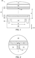
- FIG. 1 there is shown a cross-sectional view of an image sensor according to an embodiment of the present disclosure.
- an image sensor 100 shown in FIG. 1 has one pixel unit only, the image sensor 100 in practice can include a plurality of pixel units extending in x-axis direction and/or y-axis direction so as to be arranged in a matrix.
- the image sensor 100 has unlimited applications.
- the image sensor 100 performs optical under-display fingerprint sensing.
- the image sensor 100 is a front-side-illuminated (FSI) CMOS image sensor.
- the image sensor 100 includes a substrate 102, a metal stacked layer 110, a filter 120 and a microlens 122.
- the substrate 102 is doped to a first conductivity type.
- the substrate 102 is a silicon substrate which contains p-type dopants (for example, boron).
- the substrate 102 has a front side and a back side.
- the front side of the substrate 102 faces the microlens 122 and thus is irradiated by light waves.
- the backside is opposite to the front side.
- a dielectric layer 108 is disposed between the metal stacked layer 110 and the substrate 102.
- the substrate 102 includes a light collection region 104 and an isolation structure 106.
- the light collection region 104 is disposed in the substrate 102 and neighboring the front side of the substrate 102. In other words, the light collection region 104 extends from the front side of the substrate 102 toward the back side of the substrate 102 and does not extend to the back side of the substrate 102.
- the light waves admitted through the microlens 122 are converted by the light collection region 104 into photogenerated charge carriers.
- the light collection region 104 is doped to a second conductivity type opposite to the first conductivity type.
- the light collection region 104 is a silicon layer which contains n-type dopants (for example, arsenic and phosphorus).
- the aforesaid conductivity types of all components are swappable, allowing the substrate 102 and the light collection region 104 to be n-doped and p-doped, respectively.
- the isolation structure 106 is disposed around the light collection region 104.
- the isolation structure 106 is a shallow trench isolation (STI) structure.
- STI shallow trench isolation
- the metal stacked layer 110 includes a plurality of metal layers (for example, 112, 116) and a plurality of inter-metal-layer dielectric layers (for example, 114, 118) disposed between the metal layers and corresponding to the metal layers, respectively.
- the inter-metal-layer dielectric layers are made of silicon oxide, silicon oxynitride, or any material with low dielectric constant.
- the topmost metal layer 116 of the metal stacked layer 110 functions as a mask.
- the metal layer 116 has an opening 124.
- the dielectric layer 118 disposed between and corresponding to the metal layer 116.
- the inter-metal-layer dielectric layer corresponding to the metal layer where the mask is disposed extends to the opening 124 to fill the opening 124.
- the light waves admitted through the micro lens 122 pass through the opening 124 to reach the light collection region 104 so as to be converted into the photogenerated charge carriers.
- all the metal layers under the metal layer 116 must not block the light waves.
- none of the metal layers under the metal layer 116 overlaps the opening 124 from a top view.
- none of the metal layers under the metal layer 116 overlaps the opening 124 the light collection region 104.
- FIG. 2 and FIG. 3 provide schematic views of the image sensor 100.
- FIG. 2 is a partial enlarged view of the image sensor 100 shown in the cross-sectional view of FIG. 1 .
- FIG. 3 is a top view of the image sensor 100 shown in FIG. 1 .
- the opening 124 overlaps the light collection region 104 from a top view, and, owing to the position of the opening 124 and a diameter d2 of the opening 124, the opening 124 does not extend beyond the light collection region 104.
- the metal layer 116 functions as a mask providing a complete shield except for part of the light collection region 104; in other words, the metal layer 116 shields the isolation structure 106 between adjacent pixel units. Optical interference between adjacent pixel units is prevented, because the metal layer 116 blocks most of the light waves (though the metal layer 116 permits some of the light waves to enter the light collection region 104 through the opening 124.)
- the opening 124 is substantially in a round shape, and the diameter d2 of the opening 124 is configured to bring about pinhole diffraction such that a diffraction pattern which manifests circular symmetry occurs when the light waves pass through the opening 124, and the central region of the diffraction pattern has greater brightness than the peripheral region of the diffraction pattern other than the central region.
- center c of the opening 124 substantially overlaps the center of the light collection region 104, and thus the center of the diffraction pattern substantially overlaps the center of the light collection region 104. Hence, energy is concentrated at the center of the light collection region to thereby enhance the efficiency of photoelectric conversion.
- the size of the opening 124 is determined according to the wavelength of specific light waves.
- specific light waves have a wavelength of 526 nm to 606 nm
- the diameter d2 of the opening 124 is around 2.36 to 3.45 times greater than the wavelength of specific light waves.
- the size of the opening 124 is determined according to the size of the light collection region 104.
- the ratio of the diameter d2 of the opening 124 to width d3 of the light collection region 104 is 1 : 3.16 ⁇ 4.61 approximately.
- the size of the opening 124 is determined according to a distance d1 between the light collection region 104 and the opening 124.
- the ratio of the diameter d2 of the opening 124 to the distance d1 is 1 : 2.92 approximately.
- the filter 120 is disposed between the metal stacked layer 110 and the microlens 122.
- the filter 120 can be designed to be passed through by specific light waves with a specific wavelength.
- the size of the opening 124 must be designed with considerations given to the filter 120 in order to optimize specific light waves.
- any metal layer other than the topmost metal layer 116 of the metal stacked layer 110 functions as a mask.
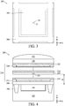
- FIG. 4 is a cross-sectional view of an image sensor according to another embodiment of the present disclosure.
- the image sensor 200 of FIG. 4 is distinguished from the image sensor 100 of FIG. 1 in that the metal layer 216 under the topmost metal layer 220 of a metal stacked layer 210 functions as a mask.
- the metal layer 216 is any metal layer other than the topmost metal layer 220 of the metal stacked layer 210.
- all the metal layers over and under the metal layer 216 must not block the light waves.
- none of the metal layers over and under the metal layer 216 overlaps the opening 224 from a top view.
- none of the metal layers over and under the metal layer 216 overlaps the light collection region 104.
- FIG. 5 is a schematic view of the image sensor for use with a handheld device according to an embodiment of the present disclosure.
- the handheld device 500 includes a display assembly 400 and an image sensor 100/200.
- the handheld device 500 performs optical under-display fingerprint sensing to sense fingerprints of a specific subject.
- the handheld device 500 is a handheld electronic device, such as smartphone, PDA, handheld computer system or panel computer.
- FIG. 6 is a cross-sectional view of the handheld device shown in FIG. 5 .
- the display assembly 400 includes a display panel 402 and a protective cover 404.
- the protective cover 404 is disposed on the display panel 400.
- the image sensor 100/200 is disposed under the display panel 400.
- the display panel 402 is an organic electroluminescence display (OLED) panel, but the present disclosure is not limited thereto.
- the handheld device 500 further includes some other components, for example, a battery 406 disposed under the image sensor 100/200.
- one of the metal layers of the metal stacked layer 110 functions as a mask, and part of the light waves passes through an opening on the metal layers, so as to reduce optical cross-talk.
- the image sensor of the present disclosure demonstrates enhanced capability to sense fingerprints without incurring additional costs.
Landscapes
- Engineering & Computer Science (AREA)
- Chemical & Material Sciences (AREA)
- Inorganic Chemistry (AREA)
- Life Sciences & Earth Sciences (AREA)
- Sustainable Development (AREA)
- Human Computer Interaction (AREA)
- Physics & Mathematics (AREA)
- General Physics & Mathematics (AREA)
- Multimedia (AREA)
- Theoretical Computer Science (AREA)
- Solid State Image Pick-Up Elements (AREA)
- Transforming Light Signals Into Electric Signals (AREA)
Abstract
Description
- The present disclosure relates to image sensors and, more particularly, to an image sensor conducive to reduction of optical cross-talk and an associated handheld device.
- Semiconductor image sensors are for use in sensing light waves. However, image sensors generate interference signals, for example, optical cross-talk, between adjacent pixels, to the detriment of performance of the image sensors. Furthermore, components at the periphery of the image sensors must be kept optically dark. When exposed to light, the components at the periphery not only manifest compromised performance but also generate interference signals.
- Therefore, it is imperative to overcome the aforesaid drawback: when image sensors are applied to optical under-display fingerprint sensing technology, optical cross-talk affects their capability to sense fingerprints.
- One of the objectives of the present disclosure is to disclose an image sensor and an associated handheld device to solve the aforementioned issues.
- An embodiment of the present disclosure discloses an image sensor. The image sensor includes: a substrate doped to a first conductivity type, the substrate having a front side and a back side, the back side being opposite to the front side; a light collection region disposed in the substrate, neighboring the front side of the substrate, and arranged to collect photogenerated charge carriers, characterized in that the light collection region is doped to a second conductivity type opposite to the first conductivity type; and a mask disposed over the substrate and the mask having an opening, allowing light waves to reach the light collection region through the opening and be converted into the photogenerated charge carriers.
- An embodiment of the present disclosure discloses a handheld device. The handheld device includes: a display assembly; and an image sensor, including the image sensor described above, for obtaining fingerprint information of the specific subject.
- According to the present disclosure, the image sensor and the handheld device demonstrate reduced optical cross-talk because the image sensor has a mask with an opening.
-
-
FIG. 1 is a cross-sectional view of an image sensor according to an embodiment of the present disclosure. -
FIG. 2 is a partial enlarged view of the image sensor shown in the cross-sectional view ofFIG. 1 . -
FIG. 3 is a top view of the image sensor shown inFIG. 1 . -
FIG. 4 is a cross-sectional view of an image sensor according to another embodiment of the present disclosure. -
FIG. 5 is a schematic view of the image sensor for use with a handheld device according to an embodiment of the present disclosure. -
FIG. 6 is a cross-sectional view of the handheld device according to an embodiment shown inFIG. 5 . - The legend is as follows:
- 100, 200
- Image sensor
- 102
- Substrate
- 104
- Light collection region
- 106
- Isolation structure
- 108
- Dielectric layer
- 110, 220
- Metal stacked layer
- 112, 116, 212, 216, 220
- Metal layer
- 114, 118, 214, 218, 222
- Inter-metallic-layer dielectric layer
- 124, 224
- Opening
- 120
- Filter
- 122
- Microlens
- d1, d2, d3
- Distance
- c
- Center
- 400
- Display assembly
- 500
- Handheld device
- 402
- Display panel
- 404
- Protective cover
- 406
- Battery
- Disclosed below are embodiments or examples illustrative of different features of the present disclosure. Specific examples of components described hereunder and configurations thereof are intended to simplify the present disclosure. Understandably, the descriptions serve illustrative purposes only but are not intended to restrict the present disclosure. For instance, in the descriptions below, the expression "forming a first feature on or over a second feature" may mean that, in an embodiment, the first and second features are in direct contact, or may mean that, in another embodiment, additional components are formed between the first and second features such that the first and second features may not be in direct contact. Furthermore, for the sake of brevity and clarity, reference numerals and/or signs may be repeatedly used in embodiments of the present disclosure without indicating any relationship between different embodiments and/or aspects.
- Position-related terms, such as "under", "below", "lower", "over", "on", and the like, are used hereunder to describe the position of a component or feature relative to another or a plurality of components or features in the accompanying drawings. In addition to relative positions in the drawings, the position-related terms indicate different directions in which a device is located when it is in use or operated. The described device may be disposed in other directions (for example, rotated by 90 degrees or in other directions). These position-related terms should be explained correspondingly.
- Although all the numerical ranges or parameters disclosed in the present disclosure are approximations, the numerical ranges or parameters express related numerical values in specific embodiments as precisely as possible. However, intrinsically, every numerical value inevitably comes with a standard deviation which arises from a testing method. The adverb "approximately" used hereunder means that the difference between the actual numerical value and a specific numerical value is less than 10%, 5%, 1% or 0.5%. Alternatively, the adverb "approximately" used hereunder means that the actual numerical value differs from the mean by a standard deviation or less, and the standard deviation is defined by persons skilled in the art. Understandably, except for empirical embodiments, or unless otherwise specified, all numerical ranges, quantity, numerical values, and percentages (for example, descriptive of the amount of a material used, time period, temperature, operation conditions, quantitative proportion, and the like) used hereunder are approximations. Therefore, unless otherwise specified, all numerical values of parameters disclosed hereunder are approximations and are subject to changes as needed. At the very least, the numerical values of parameters must be interpreted as numerical values characterized by specific significant figures and obtained by a general carry system. In this regard, a numerical value range is expressed as starting from an endpoint and ending at another endpoint or as lying between two endpoints. Unless otherwise specified, every numerical value range includes endpoints.
- The image sensor of the present disclosure reduces optical cross-talk. When applied to optical under-display fingerprint sensing technical, the image sensor of the present disclosure renders acquired fingerprint information more accurate and effectively enhances the reliability of optical under-display fingerprint sensing. The image sensor and the associated handheld device, as provided by the present disclosure, are hereunder illustrated by plurality of embodiments, depicted by the accompanying drawings, and described below.
- Referring to
FIG. 1 , there is shown a cross-sectional view of an image sensor according to an embodiment of the present disclosure. Although animage sensor 100 shown inFIG. 1 has one pixel unit only, theimage sensor 100 in practice can include a plurality of pixel units extending in x-axis direction and/or y-axis direction so as to be arranged in a matrix. Theimage sensor 100 has unlimited applications. In the embodiment illustrated byFIG. 5 and FIG. 6 , theimage sensor 100 performs optical under-display fingerprint sensing. - Particularly, in this embodiment, the
image sensor 100 is a front-side-illuminated (FSI) CMOS image sensor. Theimage sensor 100 includes asubstrate 102, a metal stackedlayer 110, afilter 120 and amicrolens 122. Thesubstrate 102 is doped to a first conductivity type. For example, thesubstrate 102 is a silicon substrate which contains p-type dopants (for example, boron). Thesubstrate 102 has a front side and a back side. The front side of thesubstrate 102 faces themicrolens 122 and thus is irradiated by light waves. The backside is opposite to the front side. In a variant embodiment, adielectric layer 108 is disposed between the metal stackedlayer 110 and thesubstrate 102. - The
substrate 102 includes alight collection region 104 and anisolation structure 106. Thelight collection region 104 is disposed in thesubstrate 102 and neighboring the front side of thesubstrate 102. In other words, thelight collection region 104 extends from the front side of thesubstrate 102 toward the back side of thesubstrate 102 and does not extend to the back side of thesubstrate 102. The light waves admitted through themicrolens 122 are converted by thelight collection region 104 into photogenerated charge carriers. Thelight collection region 104 is doped to a second conductivity type opposite to the first conductivity type. For example, thelight collection region 104 is a silicon layer which contains n-type dopants (for example, arsenic and phosphorus). However, understandably, the aforesaid conductivity types of all components are swappable, allowing thesubstrate 102 and thelight collection region 104 to be n-doped and p-doped, respectively. - The
isolation structure 106 is disposed around thelight collection region 104. Theisolation structure 106 is a shallow trench isolation (STI) structure. When theimage sensor 100 includes a plurality of pixel units, theisolation structure 106 isolates adjacent pixel units from each other so as to reduce optical cross-talk. - The metal stacked
layer 110 includes a plurality of metal layers (for example, 112, 116) and a plurality of inter-metal-layer dielectric layers (for example, 114, 118) disposed between the metal layers and corresponding to the metal layers, respectively. The inter-metal-layer dielectric layers are made of silicon oxide, silicon oxynitride, or any material with low dielectric constant. In this embodiment, thetopmost metal layer 116 of the metal stackedlayer 110 functions as a mask. Themetal layer 116 has anopening 124. Thedielectric layer 118 disposed between and corresponding to themetal layer 116. The inter-metal-layer dielectric layer corresponding to the metal layer where the mask is disposed extends to theopening 124 to fill theopening 124. The light waves admitted through themicro lens 122 pass through theopening 124 to reach thelight collection region 104 so as to be converted into the photogenerated charge carriers. In the metal stackedlayer 110, all the metal layers under themetal layer 116 must not block the light waves. For example, none of the metal layers under themetal layer 116 overlaps the opening 124 from a top view. In a variant embodiment, none of the metal layers under themetal layer 116 overlaps theopening 124 thelight collection region 104. - To further illustrate the structure of the
image sensor 100,FIG. 2 andFIG. 3 provide schematic views of theimage sensor 100.FIG. 2 is a partial enlarged view of theimage sensor 100 shown in the cross-sectional view ofFIG. 1 .FIG. 3 is a top view of theimage sensor 100 shown inFIG. 1 . As shown inFIG. 2 andFIG. 3 , theopening 124 overlaps thelight collection region 104 from a top view, and, owing to the position of theopening 124 and a diameter d2 of theopening 124, theopening 124 does not extend beyond thelight collection region 104. Therefore, from a top view, themetal layer 116 functions as a mask providing a complete shield except for part of thelight collection region 104; in other words, themetal layer 116 shields theisolation structure 106 between adjacent pixel units. Optical interference between adjacent pixel units is prevented, because themetal layer 116 blocks most of the light waves (though themetal layer 116 permits some of the light waves to enter thelight collection region 104 through theopening 124.) - In this embodiment, the
opening 124 is substantially in a round shape, and the diameter d2 of theopening 124 is configured to bring about pinhole diffraction such that a diffraction pattern which manifests circular symmetry occurs when the light waves pass through theopening 124, and the central region of the diffraction pattern has greater brightness than the peripheral region of the diffraction pattern other than the central region. In this embodiment, center c of theopening 124 substantially overlaps the center of thelight collection region 104, and thus the center of the diffraction pattern substantially overlaps the center of thelight collection region 104. Hence, energy is concentrated at the center of the light collection region to thereby enhance the efficiency of photoelectric conversion. - In an embodiment, the size of the
opening 124 is determined according to the wavelength of specific light waves. For example, specific light waves have a wavelength of 526 nm to 606 nm, the diameter d2 of theopening 124 is around 2.36 to 3.45 times greater than the wavelength of specific light waves. In a variant embodiment, the size of theopening 124 is determined according to the size of thelight collection region 104. For example, the ratio of the diameter d2 of theopening 124 to width d3 of thelight collection region 104 is 1 : 3.16 ∼ 4.61 approximately. In a variant embodiment, the size of theopening 124 is determined according to a distance d1 between thelight collection region 104 and theopening 124. For example, the ratio of the diameter d2 of theopening 124 to the distance d1 is 1 : 2.92 approximately. - The
filter 120 is disposed between the metal stackedlayer 110 and themicrolens 122. Thefilter 120 can be designed to be passed through by specific light waves with a specific wavelength. In a variant embodiment, the size of theopening 124 must be designed with considerations given to thefilter 120 in order to optimize specific light waves. - In a variant embodiment, any metal layer other than the
topmost metal layer 116 of the metal stackedlayer 110 functions as a mask. For example,FIG. 4 is a cross-sectional view of an image sensor according to another embodiment of the present disclosure. Theimage sensor 200 ofFIG. 4 is distinguished from theimage sensor 100 ofFIG. 1 in that themetal layer 216 under thetopmost metal layer 220 of a metal stackedlayer 210 functions as a mask. For example, themetal layer 216 is any metal layer other than thetopmost metal layer 220 of the metal stackedlayer 210. In the metal stackedlayer 210, all the metal layers over and under themetal layer 216 must not block the light waves. For example, none of the metal layers over and under themetal layer 216 overlaps the opening 224 from a top view. In a variant embodiment, none of the metal layers over and under themetal layer 216 overlaps thelight collection region 104. -
FIG. 5 is a schematic view of the image sensor for use with a handheld device according to an embodiment of the present disclosure. Thehandheld device 500 includes adisplay assembly 400 and animage sensor 100/200. Thehandheld device 500 performs optical under-display fingerprint sensing to sense fingerprints of a specific subject. Thehandheld device 500 is a handheld electronic device, such as smartphone, PDA, handheld computer system or panel computer.FIG. 6 is a cross-sectional view of the handheld device shown inFIG. 5 . Referring toFIG. 6 , thedisplay assembly 400 includes adisplay panel 402 and aprotective cover 404. Theprotective cover 404 is disposed on thedisplay panel 400. Theimage sensor 100/200 is disposed under thedisplay panel 400. In this embodiment, thedisplay panel 402 is an organic electroluminescence display (OLED) panel, but the present disclosure is not limited thereto. In a variant embodiment, thehandheld device 500 further includes some other components, for example, abattery 406 disposed under theimage sensor 100/200. - In the aforesaid embodiments, one of the metal layers of the metal stacked
layer 110 functions as a mask, and part of the light waves passes through an opening on the metal layers, so as to reduce optical cross-talk. When applied to optical under-display fingerprint sensing technology, the image sensor of the present disclosure demonstrates enhanced capability to sense fingerprints without incurring additional costs. - The technical features presented in embodiments of the present disclosure are concisely described above to enable persons skilled in the art to fully understand various aspects of the present disclosure. Persons skilled in the art are able to design or change any other process and structure easily in accordance with the present disclosure with a view to implementing the same objective, and/or attaining the same advantage, as the embodiments of the present disclosure. Persons skilled in the art understand that the equivalent embodiments still fall within the scope of the present disclosure and conform to the spirit thereof. Furthermore, persons skilled in the art may make various changes, substitutions and alterations to the embodiments of the present disclosure without departing from the scope and spirit of the present disclosure.
Claims (20)
- An image sensor, characterized by comprising:a substrate doped to a first conductivity type, the substrate having a front side and a back side, the back side being opposite to the front side;a light collection region disposed in the substrate and neighboring the front side of the substrate, and arranged to collect photogenerated charge carriers, wherein the light collection region is doped to a second conductivity type opposite to the first conductivity type; anda mask disposed over the substrate, and the mask having an opening allowing light waves to reach the light collection region through the opening and be converted into the photogenerated charge carriers.
- The image sensor of claim 1, characterized in that the mask is metal.
- The image sensor of claim 2, characterized by further comprising a plurality of metal layers disposed over the front side of the substrate, and the mask being disposed in one of the plurality of metal layers.
- The image sensor of claim 3, characterized in that the mask is disposed in the topmost one of the metal layers.
- The image sensor of claim 3, characterized by further comprising a plurality of inter-metal-layer dielectric layers disposed between the metal layers and corresponding to the metal layers, respectively, and the inter-metal-layer dielectric layer corresponding to the metal layer where the mask is disposed extending to the opening to fill the opening.
- The image sensor of claim 1, characterized in that, the opening overlaps the light collection region and does not extend beyond the light collection region from a top view.
- The image sensor of claim 1, characterized in that, the opening is in a round shape from a top view.
- The image sensor of claim 7, characterized in that, a center of the opening overlaps a center of the light collection region from a top view.
- The image sensor of claim 7, characterized in that the light waves pass through the opening to form a diffraction pattern which manifests circular symmetry, and a central region of the diffraction pattern has greater brightness than a peripheral region of the diffraction pattern other than the central region.
- The image sensor of claim 7, characterized in that a diameter of the opening is determined according to a wavelength of the light waves.
- The image sensor of claim 7, characterized in that a diameter of the opening is determined according to a size of the light collection region.
- The image sensor of claim 7, characterized in that a diameter of the opening is determined according to a distance between the light collection region and the opening.
- The image sensor of claim 1, characterized by further comprising a micro lens disposed over the mask.
- The image sensor of claim 13, characterized by further comprising a filter disposed between the mask and the microlens.
- The image sensor of claim 13, characterized in that, a center of the microlens overlaps the opening from a top view.
- The image sensor of claim 1, characterized by further comprising an isolation structure disposed around the light collection region.
- A handheld device, for sensing fingerprints of a specific subject, characterized by comprising:a display assembly; andthe image sensor of any one of claims 1-16 for obtaining fingerprint information of the specific subject.
- The handheld device of claim 17, characterized in that the display assembly comprises a display panel and a protective cover.
- The handheld device of claim 18, characterized in that the display panel has a first side and a second side opposite to the first side, the protective cover being disposed at the second side of the display panel, the image sensor being disposed at the first side of the display panel, and the display panel being between the image sensor and the protective cover.
- The handheld device of claim 18, characterized in that the display panel is an organic light-emitting diode display.
Applications Claiming Priority (1)
| Application Number | Priority Date | Filing Date | Title |
|---|---|---|---|
| PCT/CN2018/116317 WO2020102959A1 (en) | 2018-11-20 | 2018-11-20 | Image sensor and related handheld apparatus |
Publications (3)
| Publication Number | Publication Date |
|---|---|
| EP3686932A1 true EP3686932A1 (en) | 2020-07-29 |
| EP3686932A4 EP3686932A4 (en) | 2020-10-28 |
| EP3686932B1 EP3686932B1 (en) | 2026-01-21 |
Family
ID=66060247
Family Applications (1)
| Application Number | Title | Priority Date | Filing Date |
|---|---|---|---|
| EP18919397.2A Active EP3686932B1 (en) | 2018-11-20 | 2018-11-20 | Image sensor and related handheld apparatus |
Country Status (4)
| Country | Link |
|---|---|
| US (1) | US20200160026A1 (en) |
| EP (1) | EP3686932B1 (en) |
| CN (1) | CN109643723B (en) |
| WO (1) | WO2020102959A1 (en) |
Families Citing this family (3)
| Publication number | Priority date | Publication date | Assignee | Title |
|---|---|---|---|---|
| WO2020113380A1 (en) * | 2018-12-03 | 2020-06-11 | Boe Technology Group Co., Ltd. | Integrated photo-sensing detection display apparatus and method of fabricating integrated photo-sensing detection display apparatus |
| WO2020248286A1 (en) * | 2019-06-14 | 2020-12-17 | 深圳市汇顶科技股份有限公司 | Optical fingerprint apparatus and electronic device |
| KR102837644B1 (en) * | 2019-08-08 | 2025-07-24 | 삼성디스플레이 주식회사 | Display device |
Family Cites Families (7)
| Publication number | Priority date | Publication date | Assignee | Title |
|---|---|---|---|---|
| JP2010067840A (en) * | 2008-09-11 | 2010-03-25 | Fujifilm Corp | Solid-state imaging element and imaging apparatus |
| US8604405B2 (en) * | 2009-03-31 | 2013-12-10 | Taiwan Semiconductor Manufacturing Company, Ltd. | Backside illuminated image sensor device with refractive index dependent layer thicknesses and method of forming the same |
| KR101934864B1 (en) * | 2012-05-30 | 2019-03-18 | 삼성전자주식회사 | Through silicon via structure, methods of forming the same, image sensor including the through silicon via structure and methods of manufacturing the image sensor |
| CN103855177B (en) * | 2014-03-11 | 2016-08-24 | 格科微电子(上海)有限公司 | Imageing sensor |
| US10229316B2 (en) * | 2016-01-29 | 2019-03-12 | Synaptics Incorporated | Compound collimating system using apertures and collimators |
| CN106373973B (en) * | 2016-11-24 | 2019-11-05 | 江苏骏龙光电科技股份有限公司 | A kind of anti-interference imaging sensor |
| KR102350605B1 (en) * | 2017-04-17 | 2022-01-14 | 삼성전자주식회사 | Image sensor |
-
2018
- 2018-11-20 WO PCT/CN2018/116317 patent/WO2020102959A1/en not_active Ceased
- 2018-11-20 CN CN201880002300.XA patent/CN109643723B/en active Active
- 2018-11-20 EP EP18919397.2A patent/EP3686932B1/en active Active
-
2019
- 2019-12-04 US US16/702,959 patent/US20200160026A1/en not_active Abandoned
Also Published As
| Publication number | Publication date |
|---|---|
| US20200160026A1 (en) | 2020-05-21 |
| EP3686932B1 (en) | 2026-01-21 |
| CN109643723A (en) | 2019-04-16 |
| CN109643723B (en) | 2021-02-23 |
| WO2020102959A1 (en) | 2020-05-28 |
| EP3686932A4 (en) | 2020-10-28 |
Similar Documents
| Publication | Publication Date | Title |
|---|---|---|
| US11056523B2 (en) | Optical sensors including a light-impeding pattern | |
| US11031424B2 (en) | Image sensor with selective light-shielding for reference pixels | |
| CN109713003B (en) | Display panel and display device | |
| US6198147B1 (en) | Detecting infrared and visible light | |
| TWI791938B (en) | Optical sensor, optical sensing system and manufacturing method of optical sensor | |
| US9437635B2 (en) | Solid-state image sensor, method of manufacturing the same and camera | |
| US20190088704A1 (en) | Image sensors | |
| KR102117995B1 (en) | CMOS image sensor | |
| US20200160026A1 (en) | Image sensor and associated handheld device | |
| US12087785B2 (en) | Image sensor and manufacturing process thereof | |
| US12021098B2 (en) | Image sensor | |
| US12376405B2 (en) | Image sensor with trench structures filled with a dielectric pattern and overlapped by a light shield pattern | |
| US20220109020A1 (en) | Image sensor | |
| US9391113B2 (en) | Image-sensor device structure and method of manufacturing | |
| US20220013564A1 (en) | Image sensing device | |
| US20220114356A1 (en) | Fingerprint sensing device | |
| CN103296042A (en) | Backside-illuminated CMOS (complementary metal oxide semiconductor) image sensor and production method thereof | |
| US12588302B2 (en) | Backside deep trench isolation structure for leakage suppression | |
| TWI712959B (en) | Optical sensor and method for forming the same | |
| KR20250000652A (en) | Image sensor | |
| KR20250112624A (en) | Image sensor | |
| KR20240072804A (en) | Image sensor and manufaturing method thereof | |
| JP2006344656A (en) | Solid state imaging element and its manufacturing method |
Legal Events
| Date | Code | Title | Description |
|---|---|---|---|
| STAA | Information on the status of an ep patent application or granted ep patent |
Free format text: STATUS: UNKNOWN |
|
| STAA | Information on the status of an ep patent application or granted ep patent |
Free format text: STATUS: THE INTERNATIONAL PUBLICATION HAS BEEN MADE |
|
| PUAI | Public reference made under article 153(3) epc to a published international application that has entered the european phase |
Free format text: ORIGINAL CODE: 0009012 |
|
| STAA | Information on the status of an ep patent application or granted ep patent |
Free format text: STATUS: REQUEST FOR EXAMINATION WAS MADE |
|
| 17P | Request for examination filed |
Effective date: 20191127 |
|
| AK | Designated contracting states |
Kind code of ref document: A1 Designated state(s): AL AT BE BG CH CY CZ DE DK EE ES FI FR GB GR HR HU IE IS IT LI LT LU LV MC MK MT NL NO PL PT RO RS SE SI SK SM TR |
|
| AX | Request for extension of the european patent |
Extension state: BA ME |
|
| A4 | Supplementary search report drawn up and despatched |
Effective date: 20200925 |
|
| RIC1 | Information provided on ipc code assigned before grant |
Ipc: H01L 27/146 20060101AFI20200921BHEP |
|
| DAV | Request for validation of the european patent (deleted) | ||
| DAX | Request for extension of the european patent (deleted) | ||
| STAA | Information on the status of an ep patent application or granted ep patent |
Free format text: STATUS: EXAMINATION IS IN PROGRESS |
|
| 17Q | First examination report despatched |
Effective date: 20220422 |
|
| REG | Reference to a national code |
Ref country code: DE Ref legal event code: R079 Free format text: PREVIOUS MAIN CLASS: H01L0027146000 Ipc: H10F0039120000 Ref country code: DE Ref legal event code: R079 Ref document number: 602018088788 Country of ref document: DE Free format text: PREVIOUS MAIN CLASS: H01L0027146000 Ipc: H10F0039120000 |
|
| GRAP | Despatch of communication of intention to grant a patent |
Free format text: ORIGINAL CODE: EPIDOSNIGR1 |
|
| STAA | Information on the status of an ep patent application or granted ep patent |
Free format text: STATUS: GRANT OF PATENT IS INTENDED |
|
| RIC1 | Information provided on ipc code assigned before grant |
Ipc: H10F 39/12 20250101AFI20250926BHEP Ipc: H10K 59/65 20230101ALI20250926BHEP Ipc: G06V 40/13 20220101ALI20250926BHEP Ipc: H10F 39/00 20250101ALI20250926BHEP |
|
| INTG | Intention to grant announced |
Effective date: 20251021 |
|
| GRAS | Grant fee paid |
Free format text: ORIGINAL CODE: EPIDOSNIGR3 |
|
| GRAA | (expected) grant |
Free format text: ORIGINAL CODE: 0009210 |
|
| STAA | Information on the status of an ep patent application or granted ep patent |
Free format text: STATUS: THE PATENT HAS BEEN GRANTED |
|
| AK | Designated contracting states |
Kind code of ref document: B1 Designated state(s): AL AT BE BG CH CY CZ DE DK EE ES FI FR GB GR HR HU IE IS IT LI LT LU LV MC MK MT NL NO PL PT RO RS SE SI SK SM TR |
|
| REG | Reference to a national code |
Ref country code: CH Ref legal event code: F10 Free format text: ST27 STATUS EVENT CODE: U-0-0-F10-F00 (AS PROVIDED BY THE NATIONAL OFFICE) Effective date: 20260121 |
|
| REG | Reference to a national code |
Ref country code: DE Ref legal event code: R096 Ref document number: 602018088788 Country of ref document: DE |
|
| REG | Reference to a national code |
Ref country code: IE Ref legal event code: FG4D |
|
| REG | Reference to a national code |
Ref country code: NL Ref legal event code: MP Effective date: 20260121 |
|
| PG25 | Lapsed in a contracting state [announced via postgrant information from national office to epo] |
Ref country code: NL Free format text: LAPSE BECAUSE OF FAILURE TO SUBMIT A TRANSLATION OF THE DESCRIPTION OR TO PAY THE FEE WITHIN THE PRESCRIBED TIME-LIMIT Effective date: 20260121 |
|
| REG | Reference to a national code |
Ref country code: AT Ref legal event code: MK05 Ref document number: 1879778 Country of ref document: AT Kind code of ref document: T Effective date: 20260121 |
|
| PG25 | Lapsed in a contracting state [announced via postgrant information from national office to epo] |
Ref country code: RS Free format text: LAPSE BECAUSE OF FAILURE TO SUBMIT A TRANSLATION OF THE DESCRIPTION OR TO PAY THE FEE WITHIN THE PRESCRIBED TIME-LIMIT Effective date: 20260421 |
|
| PG25 | Lapsed in a contracting state [announced via postgrant information from national office to epo] |
Ref country code: ES Free format text: LAPSE BECAUSE OF FAILURE TO SUBMIT A TRANSLATION OF THE DESCRIPTION OR TO PAY THE FEE WITHIN THE PRESCRIBED TIME-LIMIT Effective date: 20260121 |
|
| PG25 | Lapsed in a contracting state [announced via postgrant information from national office to epo] |
Ref country code: PL Free format text: LAPSE BECAUSE OF FAILURE TO SUBMIT A TRANSLATION OF THE DESCRIPTION OR TO PAY THE FEE WITHIN THE PRESCRIBED TIME-LIMIT Effective date: 20260121 |
|
| PG25 | Lapsed in a contracting state [announced via postgrant information from national office to epo] |
Ref country code: GR Free format text: LAPSE BECAUSE OF FAILURE TO SUBMIT A TRANSLATION OF THE DESCRIPTION OR TO PAY THE FEE WITHIN THE PRESCRIBED TIME-LIMIT Effective date: 20260422 |
|
| REG | Reference to a national code |
Ref country code: LT Ref legal event code: MG9D |
|
| PG25 | Lapsed in a contracting state [announced via postgrant information from national office to epo] |
Ref country code: LT Free format text: LAPSE BECAUSE OF FAILURE TO SUBMIT A TRANSLATION OF THE DESCRIPTION OR TO PAY THE FEE WITHIN THE PRESCRIBED TIME-LIMIT Effective date: 20260121 |
|
| PG25 | Lapsed in a contracting state [announced via postgrant information from national office to epo] |
Ref country code: NO Free format text: LAPSE BECAUSE OF FAILURE TO SUBMIT A TRANSLATION OF THE DESCRIPTION OR TO PAY THE FEE WITHIN THE PRESCRIBED TIME-LIMIT Effective date: 20260421 |
|
| PG25 | Lapsed in a contracting state [announced via postgrant information from national office to epo] |
Ref country code: AT Free format text: LAPSE BECAUSE OF FAILURE TO SUBMIT A TRANSLATION OF THE DESCRIPTION OR TO PAY THE FEE WITHIN THE PRESCRIBED TIME-LIMIT Effective date: 20260121 Ref country code: FI Free format text: LAPSE BECAUSE OF FAILURE TO SUBMIT A TRANSLATION OF THE DESCRIPTION OR TO PAY THE FEE WITHIN THE PRESCRIBED TIME-LIMIT Effective date: 20260121 Ref country code: SE Free format text: LAPSE BECAUSE OF FAILURE TO SUBMIT A TRANSLATION OF THE DESCRIPTION OR TO PAY THE FEE WITHIN THE PRESCRIBED TIME-LIMIT Effective date: 20260121 |
|
| PG25 | Lapsed in a contracting state [announced via postgrant information from national office to epo] |
Ref country code: HR Free format text: LAPSE BECAUSE OF FAILURE TO SUBMIT A TRANSLATION OF THE DESCRIPTION OR TO PAY THE FEE WITHIN THE PRESCRIBED TIME-LIMIT Effective date: 20260121 |
|
| PG25 | Lapsed in a contracting state [announced via postgrant information from national office to epo] |
Ref country code: IS Free format text: LAPSE BECAUSE OF FAILURE TO SUBMIT A TRANSLATION OF THE DESCRIPTION OR TO PAY THE FEE WITHIN THE PRESCRIBED TIME-LIMIT Effective date: 20260521 Ref country code: PT Free format text: LAPSE BECAUSE OF FAILURE TO SUBMIT A TRANSLATION OF THE DESCRIPTION OR TO PAY THE FEE WITHIN THE PRESCRIBED TIME-LIMIT Effective date: 20260521 |
|
| PG25 | Lapsed in a contracting state [announced via postgrant information from national office to epo] |
Ref country code: LV Free format text: LAPSE BECAUSE OF FAILURE TO SUBMIT A TRANSLATION OF THE DESCRIPTION OR TO PAY THE FEE WITHIN THE PRESCRIBED TIME-LIMIT Effective date: 20260121 |
|
| PG25 | Lapsed in a contracting state [announced via postgrant information from national office to epo] |
Ref country code: BG Free format text: LAPSE BECAUSE OF FAILURE TO SUBMIT A TRANSLATION OF THE DESCRIPTION OR TO PAY THE FEE WITHIN THE PRESCRIBED TIME-LIMIT Effective date: 20260121 |