EP3686929A1 - Semiconductor die - Google Patents
Semiconductor die Download PDFInfo
- Publication number
- EP3686929A1 EP3686929A1 EP19153518.6A EP19153518A EP3686929A1 EP 3686929 A1 EP3686929 A1 EP 3686929A1 EP 19153518 A EP19153518 A EP 19153518A EP 3686929 A1 EP3686929 A1 EP 3686929A1
- Authority
- EP
- European Patent Office
- Prior art keywords
- gate
- region
- gate pad
- polysilicon
- pad
- Prior art date
- Legal status (The legal status is an assumption and is not a legal conclusion. Google has not performed a legal analysis and makes no representation as to the accuracy of the status listed.)
- Granted
Links
Images




Classifications
-
- H—ELECTRICITY
- H10—SEMICONDUCTOR DEVICES; ELECTRIC SOLID-STATE DEVICES NOT OTHERWISE PROVIDED FOR
- H10D—INORGANIC ELECTRIC SEMICONDUCTOR DEVICES
- H10D89/00—Aspects of integrated devices not covered by groups H10D84/00 - H10D88/00
- H10D89/60—Integrated devices comprising arrangements for electrical or thermal protection, e.g. protection circuits against electrostatic discharge [ESD]
- H10D89/601—Integrated devices comprising arrangements for electrical or thermal protection, e.g. protection circuits against electrostatic discharge [ESD] for devices having insulated gate electrodes, e.g. for IGFETs or IGBTs
- H10D89/611—Integrated devices comprising arrangements for electrical or thermal protection, e.g. protection circuits against electrostatic discharge [ESD] for devices having insulated gate electrodes, e.g. for IGFETs or IGBTs using diodes as protective elements
-
- H—ELECTRICITY
- H10—SEMICONDUCTOR DEVICES; ELECTRIC SOLID-STATE DEVICES NOT OTHERWISE PROVIDED FOR
- H10D—INORGANIC ELECTRIC SEMICONDUCTOR DEVICES
- H10D30/00—Field-effect transistors [FET]
- H10D30/60—Insulated-gate field-effect transistors [IGFET]
- H10D30/64—Double-diffused metal-oxide semiconductor [DMOS] FETs
- H10D30/66—Vertical DMOS [VDMOS] FETs
- H10D30/665—Vertical DMOS [VDMOS] FETs having edge termination structures
-
- H—ELECTRICITY
- H10—SEMICONDUCTOR DEVICES; ELECTRIC SOLID-STATE DEVICES NOT OTHERWISE PROVIDED FOR
- H10D—INORGANIC ELECTRIC SEMICONDUCTOR DEVICES
- H10D62/00—Semiconductor bodies, or regions thereof, of devices having potential barriers
- H10D62/10—Shapes, relative sizes or dispositions of the regions of the semiconductor bodies; Shapes of the semiconductor bodies
- H10D62/102—Constructional design considerations for preventing surface leakage or controlling electric field concentration
- H10D62/103—Constructional design considerations for preventing surface leakage or controlling electric field concentration for increasing or controlling the breakdown voltage of reverse-biased devices
- H10D62/105—Constructional design considerations for preventing surface leakage or controlling electric field concentration for increasing or controlling the breakdown voltage of reverse-biased devices by having particular doping profiles, shapes or arrangements of PN junctions; by having supplementary regions, e.g. junction termination extension [JTE]
- H10D62/109—Reduced surface field [RESURF] PN junction structures
- H10D62/111—Multiple RESURF structures, e.g. double RESURF or 3D-RESURF structures
-
- H—ELECTRICITY
- H10—SEMICONDUCTOR DEVICES; ELECTRIC SOLID-STATE DEVICES NOT OTHERWISE PROVIDED FOR
- H10D—INORGANIC ELECTRIC SEMICONDUCTOR DEVICES
- H10D84/00—Integrated devices formed in or on semiconductor substrates that comprise only semiconducting layers, e.g. on Si wafers or on GaAs-on-Si wafers
- H10D84/101—Integrated devices comprising main components and built-in components, e.g. IGBT having built-in freewheel diode
- H10D84/141—VDMOS having built-in components
-
- H—ELECTRICITY
- H10—SEMICONDUCTOR DEVICES; ELECTRIC SOLID-STATE DEVICES NOT OTHERWISE PROVIDED FOR
- H10D—INORGANIC ELECTRIC SEMICONDUCTOR DEVICES
- H10D84/00—Integrated devices formed in or on semiconductor substrates that comprise only semiconducting layers, e.g. on Si wafers or on GaAs-on-Si wafers
- H10D84/101—Integrated devices comprising main components and built-in components, e.g. IGBT having built-in freewheel diode
- H10D84/141—VDMOS having built-in components
- H10D84/148—VDMOS having built-in components the built-in components being breakdown diodes, e.g. Zener diodes
-
- H—ELECTRICITY
- H10—SEMICONDUCTOR DEVICES; ELECTRIC SOLID-STATE DEVICES NOT OTHERWISE PROVIDED FOR
- H10D—INORGANIC ELECTRIC SEMICONDUCTOR DEVICES
- H10D89/00—Aspects of integrated devices not covered by groups H10D84/00 - H10D88/00
- H10D89/60—Integrated devices comprising arrangements for electrical or thermal protection, e.g. protection circuits against electrostatic discharge [ESD]
- H10D89/601—Integrated devices comprising arrangements for electrical or thermal protection, e.g. protection circuits against electrostatic discharge [ESD] for devices having insulated gate electrodes, e.g. for IGFETs or IGBTs
- H10D89/921—Integrated devices comprising arrangements for electrical or thermal protection, e.g. protection circuits against electrostatic discharge [ESD] for devices having insulated gate electrodes, e.g. for IGFETs or IGBTs characterised by the configuration of the interconnections connecting the protective arrangements, e.g. ESD buses
-
- H—ELECTRICITY
- H10—SEMICONDUCTOR DEVICES; ELECTRIC SOLID-STATE DEVICES NOT OTHERWISE PROVIDED FOR
- H10D—INORGANIC ELECTRIC SEMICONDUCTOR DEVICES
- H10D89/00—Aspects of integrated devices not covered by groups H10D84/00 - H10D88/00
- H10D89/60—Integrated devices comprising arrangements for electrical or thermal protection, e.g. protection circuits against electrostatic discharge [ESD]
- H10D89/601—Integrated devices comprising arrangements for electrical or thermal protection, e.g. protection circuits against electrostatic discharge [ESD] for devices having insulated gate electrodes, e.g. for IGFETs or IGBTs
- H10D89/931—Integrated devices comprising arrangements for electrical or thermal protection, e.g. protection circuits against electrostatic discharge [ESD] for devices having insulated gate electrodes, e.g. for IGFETs or IGBTs characterised by the dispositions of the protective arrangements
-
- H—ELECTRICITY
- H10—SEMICONDUCTOR DEVICES; ELECTRIC SOLID-STATE DEVICES NOT OTHERWISE PROVIDED FOR
- H10W—GENERIC PACKAGES, INTERCONNECTIONS, CONNECTORS OR OTHER CONSTRUCTIONAL DETAILS OF DEVICES COVERED BY CLASS H10
- H10W20/00—Interconnections in chips, wafers or substrates
- H10W20/40—Interconnections external to wafers or substrates, e.g. back-end-of-line [BEOL] metallisations or vias connecting to gate electrodes
- H10W20/41—Interconnections external to wafers or substrates, e.g. back-end-of-line [BEOL] metallisations or vias connecting to gate electrodes characterised by their conductive parts
- H10W20/42—Vias, e.g. via plugs
-
- H—ELECTRICITY
- H10—SEMICONDUCTOR DEVICES; ELECTRIC SOLID-STATE DEVICES NOT OTHERWISE PROVIDED FOR
- H10D—INORGANIC ELECTRIC SEMICONDUCTOR DEVICES
- H10D64/00—Electrodes of devices having potential barriers
- H10D64/20—Electrodes characterised by their shapes, relative sizes or dispositions
- H10D64/27—Electrodes not carrying the current to be rectified, amplified, oscillated or switched, e.g. gates
- H10D64/311—Gate electrodes for field-effect devices
- H10D64/411—Gate electrodes for field-effect devices for FETs
- H10D64/511—Gate electrodes for field-effect devices for FETs for IGFETs
- H10D64/517—Gate electrodes for field-effect devices for FETs for IGFETs characterised by the conducting layers
Definitions
- lateral or lateral direction should be understood to mean a direction or extent that runs generally parallel to the lateral extent of a semiconductor material or semiconductor carrier.
- the lateral direction thus extends generally parallel to these surfaces or sides.
- vertical or “vertical direction” is understood to mean a direction that runs generally perpendicular to these surfaces or sides and thus to the lateral direction. The vertical direction therefore runs in the thickness direction of the semiconductor material or semiconductor carrier.
- a single continuous ESD protection diode includes at least one concave section that extends around a corner of the gate pad and a convex section at one end or a convex section at each end in order to increase the width of the ESD protection diode.
- ESD HBM Human Body Model
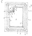
- Figure 1 illustrates a top view of a semiconductor die 20 having a semiconductor chip layout 21.
- the semiconductor die 20 includes a semiconductor body having a first major surface 22.
- the semiconductor body may be formed of silicon.
- the semiconductor die 20 and the semiconductor chip layout 21 include a transistor device 23 which includes a cell field 24 and an edge termination region 25.
- the transistor device 23 is a vertical transistor device with a vertical drift path.
- the transistor device 23 is a superjunction device.
- the transistor device 23 is an IGBT device.
- the superjunction device and the IGBT device are examples of vertical transistor devices.
- a passivation layer such as a polyimide may be arranged on the gate pad 28 and source pad 27 and include openings above the gate pad 28 and the source pad 27, respectively, to provide an exposed portion which provides a contact area.
- This contact area can be called a pad, in which case the source pad 27 is called a source metal or source metal layer and the gate pad 28 is called a gate metal or gate metal layer.
- the source pad 27 and gate pad 28 may include two or more sublayers of differing composition and the metal may be an alloy.
- the shielding region 31 includes a non-depletable doped region 62 (not illustrated in figures 1 and 2 ) .
- the gate polysilicon layer 43 extends continuously and uninterruptedly under the gate pad 28.
- the gate polysilicon layer 43 includes openings in which the polysilicon ESD protection diode 32 is positioned so that the gate polysilicon layer 43 is laterally spaced apart from the polysilicon ESD protection diode 32.
- the semiconductor die 20 includes a plurality of transistor cells 50 which together provide the transistor device 23.
- the transistor device 23 is a superjunction transistor device 23.
- the superjunction transistor device 23 includes a plurality of doped columns of opposing conductivity extending into the body of the semiconductor die 20 substantially perpendicularly to the first major surface 22.
- the columns of opposing conductivity are arranged laterally alternately, for example a first column 51 comprising a first conductivity type, is arranged laterally adjacent a second column 52 comprising a second conductivity type that is in turn arranged laterally adjacent a third column 53 including the first conductivity type and so on.
- the first and third columns 51, 53 of the first conductivity type provide the drift region and the second columns 52 of the second conductivity type provide the compensation regions of the superjunction transistor cell 50.
- the shielding region 31 comprises a non-depletable doped region 62 and a depletable doped region 63 which are contiguous to one another such that a boundary 64 is formed therebetween.
- the non-depletable doped region 62 and a depletable doped region 63 are doped with the second conductivity type.
- the non-depletable doped region 62 may comprise a maximum doping concentration of 8*10 15 cm -3 to 1*10 17 cm -3 .
- the depletable doped region 63 may comprise a maximum doping concentration of 5*10 11 cm -3 to 8*10 15 cm -3 .
- a second insulating layer 67 is arranged on the shielding region 31 and may include an oxide.
- the polysilicon ESD protection diode 32 and the gate polysilicon layer 43 are arranged on the second insulating layer 67.
- the first insulating layer 61 is positioned on the polysilicon ESD protection diode 32 and the gate polysilicon layer 43.
- the second insulating layer 67 may be referred to as a field oxide.
- the non-depletable doped region 62 of the shielding region 31 comprises a doping concentration that is non-depletable by voltages applied to the superjunction transistor device 23 during a blocking mode of the superjunction transistor device 23.
- the lateral area of the polysilicon ESD protection diode 32 is less than that of the shielding region 31.
- the shielding region 31 can be used to reduce a leakage current or back gate effect of the polysilicon ESD protection diode 32 during operation.
- the formation of channels or turn-on of a parasitic transistor structure is avoided and may be used to reduce power consumption and degradation of the polysilicon ESD protection diode 32.
- the shielding region 31 may have different forms.
- the shielding region 31 includes the non-depletable doped region 62 only.
- the non-depletable region 62 of the shielding region 31 may have a lateral extent such that an outermost edge, that is an outermost edge with respect to a direction extending from the cell field 24 in the direction of the edge termination region 25 and the side face 26 of the semiconductor die 20, of the non-depletable region 62 is positioned vertically under the polysilicon ESD protection diode 32.
- the innermost edge may is positioned vertically under the source pad 27.
- the non-depletable region 62 of the shielding region 31 has a lateral extent such that the outermost edge of the non-depletable region 62 extends further into the edge termination region 25 than the polysilicon ESD protection diode 32 and may be positioned vertically under the gate pad 28.
- the gate polysilicon layer 43 is positioned on the second insulation layer 67 and electrically couples the gate electrodes 59 of the transistor cells 50 to the gate pad 28 and the gate runner 41.
- the gate polysilicon layer 43 is positioned on the second insulation layer 67 and is covered by the first insulation layer 61.
- the gate polysilicon layer is coupled to the gate pad 28 by one or more conductive vias 73 and to the gate runner 41 by one or more conductive vias 74.
- the gate connection 72 is laterally spaced apart from the two separate sections 33, 34 of the polysilicon ESD protection diode 32.
- the polysilicon gate connection 72 provides a conductive path between some of the gate electrodes 59 in the cell field 24 and the gate pad 28 without the gate runner 41.
- the polysilicon gate connection 72 is connected to the gate pad 28 by the conductive via 73.
- Figure 7 illustrates a top view of a semiconductor die 20' with a chip layout 21' which differs from that illustrated in figures 1 to 6 in the form of the polysilicon ESD protection diode 32'.
- the polysilicon ESD protection diode 32 includes two sections 33' 34' which are arranged on two substantially orthogonal sides of the gate pad 28 as in the embodiments illustrated in figures 1 to 6 . Again as illustrated in the embodiments illustrated in figures 1 to 6 , each of the sections 33', 34' partially vertically overlaps with the shielding region 31 and the source metal pad 27 and with the gate pad 28.
- the polysilicon ESD protection diode 32 therefore, includes the extensions 82, 83 illustrated in figure 7 at opposing ends of a single section polysilicon ESD protection diode 32".
- the gate pad 28' includes the curved portions 85, 86 which overlap with the curved portions 88, 89 of the polysilicon ESD protection diode 32" as in the embodiment illustrated in figure 7 .
- the extensions 81, 82 (for example of the embodiment illustrated in Figure 7 ) and convex portions 88, 89 (for example of the embodiment illustrated in Figure 8 ) of the polysilicon ESD protection diode 32', 32", respectively, may be used to increase the width of the ESD polysilicon diode 32', 32", respectively, and its ESD HBM protection rating.
- the concave portion 85 has a radius of curvature R1 which is less than the radius of curvature R2 of the convex portions 88, 89 providing the extensions 81, 82 so that R1 ⁇ R2. In some embodiments, R2 > 4R1.
- Figures 9 to 11 illustrate top views of a semiconductor die with a superjunction transistor device that includes a chip layout which differs from the chip layout of the embodiments illustrated in figures 1 to 8 in the position of the gate pad in relation to the sidewalls of the first surface of the semiconductor die.
- the shielding region which underlies the polysilicon ESD protection diode 132' and surrounds the cell field 124 has a lateral form corresponding to the outer contour of the source pad 127 illustrated in the top view of figure 10 .
- the curved extensions 182, 182' are, therefore, positioned vertically above curved portions of the shielding region and have a lateral from corresponding to the lateral form of the shielding region so that the polysilicon ESD protection diode 132' including the extensions 182, 182' are electrically shielded from the underlying drift region 51 and compensation region 52 (not shown in the top view of figure 10 ) by the intermediately positioned shielding region (not shown in the top view of figure 10 ) .
- the semiconductor die includes an integrated non-depletable region 62, which extends further into the edge termination region 25 than the polysilicon ESD diode 32.
Landscapes
- Semiconductor Integrated Circuits (AREA)
- Metal-Oxide And Bipolar Metal-Oxide Semiconductor Integrated Circuits (AREA)
Abstract
Description
- Semiconductor devices may be subjected to various effects which can lead to damage of the semiconductor device. For example, semiconductor devices may be subjected to electrostatic discharge (ESD) events.
US 2018/0090479 A1 discloses a semiconductor device comprising a transistor arrangement with a diode structure coupled between a gate structure and a source structure of the transistor arrangement. The diode structure is intended to provide protection for the transistor arrangement against ESD events. However, further improvements to the protection provided for semiconductor devices against ESD events are desirable. - In an embodiment, a semiconductor die comprises a transistor device that comprises a cell field and an edge termination region, a source pad arranged on the cell field, a gate pad arranged laterally adjacent the cell field and in the edge termination region, a shielding region laterally surrounding the cell field, the shielding region comprising a non-depletable doped region. The polysilicon ESD protection diode is arranged laterally between the gate pad and the source pad and vertically above at least a portion of the shielding region. The polysilicon ESD protection diode comprises at least two separate sections that are electrically coupled in parallel between the gate pad and the source pad. The sections are laterally spaced apart by a gap situated at a corner of the gate pad.
- In an embodiment, a semiconductor die comprises a transistor device that comprises a cell field and an edge termination region, a source pad arranged on the cell field, a gate pad laterally arranged laterally adjacent the cell field and in the edge termination region, a shielding region laterally surrounding the cell field, the shielding region comprising a non-depletable doped region. The polysilicon ESD protection diode is arranged laterally between the gate pad and the source pad and vertically above at least a portion of the shielding region. The polysilicon ESD protection diode extends along two adjoining sides of the gate pad and comprises a concave portion extending around a corner of the gate pad formed between the two adjoining sides and a convex portion that extends away from the gate pad at each end of the polysilicon ESD protection diode.
- Those skilled in the art will recognize additional features and advantages upon reading the following detailed description, and upon viewing the accompanying drawings.
- The elements of the drawings are not necessarily to scale relative to each other. Like reference numerals designate corresponding similar parts. The features of the various illustrated embodiments can be combined unless they exclude each other. Exemplary embodiments are depicted in the drawings and are detailed in the description which follows.
-
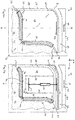
Figure 1 illustrates a top view of a semiconductor die according to an embodiment. -
Figure 2 , which includesfigures 2a and 2b , includes enlarged views of the gate pad of the semiconductor die offigure 1 according to two embodiments. -
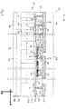
Figure 3 illustrates a cross-sectional view along the line A-A offigure 2a . -
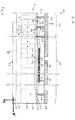
Figure 4 illustrates a cross-sectional view along the line B-B infigure 2a . -
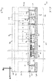
Figure 5 illustrates a cross-sectional view A'-A' corresponding to the line A-A infigure 2a and illustrates a gate resistor. -
Figure 6 illustrates a cross-sectional view along the line A-A offigure 2b and illustrates a gate resistor according to another embodiment. -
Figure 7 illustrates a top view of a semiconductor die according to an embodiment. -
Figure 8 illustrates a top view of a semiconductor die according to an embodiment. -
Figure 9 illustrates a top view of a semiconductor die according to an embodiment. -
Figure 10 illustrates a top view of a semiconductor die according to an embodiment. -
Figure 11 illustrates a top view of a semiconductor die according to an embodiment. - In the following detailed description, reference is made to the accompanying drawings, which form a part hereof, and in which is shown by way of illustration specific embodiments in which the invention may be practiced. In this regard, directional terminology, such as "top", "bottom", "front", "back", "leading", "trailing", etc., is used with reference to the orientation of the figure(s) being described. Because components of the embodiments can be positioned in a number of different orientations, the directional terminology is used for purposes of illustration and is in no way limiting. It is to be understood that other embodiments may be utilized and structural or logical changes may be made without departing from the scope of the present invention. The following detailed description, thereof, is not to be taken in a limiting sense, and the scope of the present invention is defined by the appended claims.
- A number of exemplary embodiments will be explained below. In this case, identical structural features are identified by identical or similar reference symbols in the figures. In the context of the present description, "lateral" or "lateral direction" should be understood to mean a direction or extent that runs generally parallel to the lateral extent of a semiconductor material or semiconductor carrier. The lateral direction thus extends generally parallel to these surfaces or sides. In contrast thereto, the term "vertical" or "vertical direction" is understood to mean a direction that runs generally perpendicular to these surfaces or sides and thus to the lateral direction. The vertical direction therefore runs in the thickness direction of the semiconductor material or semiconductor carrier.
- As employed in this specification, when an element such as a layer, region or substrate is referred to as being "on" or extending "onto" another element, it can be directly on or extend directly onto the other element or intervening elements may also be present. In contrast, when an element is referred to as being "directly on" or extending "directly onto" another element, there are no intervening elements present.
- As employed in this specification, when an element is referred to as being "connected" or "coupled" to another element, it can be directly connected or coupled to the other element or intervening elements may be present. In contrast, when an element is referred to as being "directly connected" or "directly coupled" to another element, there are no intervening elements present.
- In an embodiment, a semiconductor die is provided which includes a superjunction transistor device and an integrated diode for protecting the superjunction transistor device against electrostatic discharge (ESD). An example of a superjunction transistor device is a CoolMOS® device.
- Superjunction devices typically have a predefined area which is typically kept small in order to reduce the active area and Rds(on) for the device. This, however, restricts the amount of space available for including additional devices such as an ESD protection diode in the same semiconductor die as the superjunction transistor device. If the ESD protection diode is integrated into the area around the gate pad, the space available for the ESD protection diode is also restricted since the area of the gate pad is typically kept as small as possible so as not to increase the overall size of the die.
- The semiconductor die may include other types of transistor device in place of the superjunction transistor device. In some embodiments, a semiconductor die is provided that includes a vertical transistor device, that is a transistor device with a vertical drift path, and an integrated diode for protecting the vertical transistor device against electrostatic discharge. In some embodiments, a semiconductor die is provided which includes an IGBT (Insulated Gate Bipolar Transistor) device and an integrated diode for protecting the IGBT transistor device against electrostatic discharge (ESD).
- In some embodiments, the ESD protection device is provided in the form of a polysilicon ESD protection device which includes two sections that are spaced apart from one another and extend substantially perpendicularly to one another in a top view of the semiconductor die. These sections may be arranged laterally between the gate pad and the source pad of the transistor device such that the gap between the sections is arranged at a corner of the gate pad. Each section may comprise multiple diodes, in particular, ESD protection diodes and the multiple ESD protection diodes and the two sections are electrically coupled in parallel between the gate pad and the source pad and consequently between the gate and source electrodes of the transistor device.
- The provision of multiple separate sections positioned between the gate pad and the source pad is used to avoid a concave section in the ESD protection diode in plan view, typically at the corner or corners of the gate pad, in which current crowding and locally increased electric fields could otherwise occur which can, in some ESD events, lead to an increased risk of destroying the ESD protection diode. At the same time, the total width of the ESD protection diode is reduced by only a small amount over an arrangement in which the two sections are joined by a concave section around the corner to provide a single ESD protection diode. This is useful as the width of the ESD protection diode is a parameter in determining the protection rating provided by the ESD protection diode.
- In some embodiments, the width of the ESD protection diode is increased by the provision of a convex extension at the distal end of one or two sections of the ESD protection diodes. The convex extension extends away from the gate pad and has a curved form which may be aligned or substantially concentric with an outer contour of the source pad.
- In an alternative embodiment, a single continuous ESD protection diode is provided that includes at least one concave section that extends around a corner of the gate pad and a convex section at one end or a convex section at each end in order to increase the width of the ESD protection diode. Thus the ESD HBM (Human Body Model) capability of the semiconductor die is increased without requiring an increase in the area of the semiconductor die or without restricting the area of the semiconductor die used for the active device, i.e. transistor device such as a the superjunction transistor device or a IGBT device, by occupying this area with the ESD protection diode.
- The electrodes or terminals of the transistor device are referred to herein as source, drain and gate. As used herein, these terms also encompass the functionally equivalent terminals of other types of transistor devices, such as an insulated gate bipolar transistor (IGBT). For example, as used herein, the term "source" encompasses not only a source of a MOSFET device and of a superjunction device but also an emitter of an insulator gate bipolar transistor (IGBT) device, the term "drain" encompasses not only a drain of a MOSFET device or of a superjunction device but also a collector of an insulator gate bipolar transistor (IGBT) device, and the term "gate" encompasses not only a gate of a MOSFET device or of a superjunction device but also a gate of an insulator gate bipolar transistor (IGBT) device.
-
Figure 1 illustrates a top view of asemiconductor die 20 having asemiconductor chip layout 21. The semiconductor die 20 includes a semiconductor body having a firstmajor surface 22. The semiconductor body may be formed of silicon. The semiconductor die 20 and thesemiconductor chip layout 21 include atransistor device 23 which includes acell field 24 and anedge termination region 25. In some embodiments, thetransistor device 23 is a vertical transistor device with a vertical drift path. In some embodiments, thetransistor device 23 is a superjunction device. In other embodiments, thetransistor device 23 is an IGBT device. The superjunction device and the IGBT device are examples of vertical transistor devices. - The
edge termination region 25 laterally surrounds thecell field 24 and is positioned at the periphery of the firstmajor surface 22adjacent sidewalls 26 of the semiconductor die 20 which define the lateral extent of the firstmajor surface 22. The semiconductor die 20 includes asource pad 27 which is arranged on thecell field 24 and comprises metal and agate pad 28 which is positioned laterally adjacent thecell field 24 and in theedge termination region 25. Thegate pad 28 comprises metal. The outer contour of thesource pad 27 is positioned laterally adjacent and spaced apart from the two adjoiningsides gate pad 28. For a vertical transistor device, such as a superjunction transistor device, thesource pad 27 andgate pad 28 are positioned on the firstmajor surface 22 of the semiconductor die 20 and a drain pad is positioned on the opposing major surface of the semiconductor die 20. - A passivation layer such as a polyimide may be arranged on the
gate pad 28 andsource pad 27 and include openings above thegate pad 28 and thesource pad 27, respectively, to provide an exposed portion which provides a contact area. This contact area can be called a pad, in which case thesource pad 27 is called a source metal or source metal layer and thegate pad 28 is called a gate metal or gate metal layer. Thesource pad 27 andgate pad 28 may include two or more sublayers of differing composition and the metal may be an alloy. - In the embodiment illustrated in
figure 1 , thegate pad 28 is positioned towards a corner of the firstmajor surface 22 and has a substantially square or rectangular form such that thecell field 24 is positioned laterally adjacent to adjoiningsides gate pad 28. - The semiconductor die 20 further comprises a shielding
region 31 which extends from thefirst surface 22 into the semiconductor body and which laterally surrounds thecell field 24. The shieldingregion 31 has the form of an uninterrupted and continuous ring that has a lateral form that is substantially aligned with the outer contour of thesource pad 27. Both the shieldingregion 31 and thecell field 24 are positioned laterally adjacent the twosides gate pad 28. The shieldingregion 31 has a lateral extent such that it extends under the periphery of thesource pad 27 and is positioned vertically underneath the outer contour of thesource pad 27 and such that it extends laterally into theedge termination region 25. - In some embodiments, the shielding
region 31 includes a non-depletable doped region 62 (not illustrated infigures 1 and2 ) . - In some embodiments, the shielding
region 31 includes a non-depletabledoped region 62 and further includes a depletable doped region (not illustrated infigures 1 and2 ) which are laterally contiguous to one another such that aboundary 64 is formed between the non-depletable doped region and the depletable doped region. The position of the depletable dopedregion 63 as well as theboundary 64 and the non-depletabledoped region 62 can be seen in the cross-sectional views offigures 3 to 6 . - The semiconductor die 20 further comprises an integrated ESD (Electrostatic Discharge) protection diode in the form of a
polysilicon ESD diode 32. The polysiliconESD protection diode 32 is positioned laterally between thegate pad 28 and thesource pad 27 and is positioned vertically above at least a portion of the shieldingregion 31. In embodiments in which the shielding region comprises a laterally contiguous non-depletabledoped region 62 and depletable dopedregion 63 with aboundary 64 therebetween, the polysiliconESD protection diode 31 may be arranged vertically above theboundary 64 between the non-depletabledoped region 62 and the depletable dopedregion 63 of the shieldingregion 31. The polysiliconESD protection diode 32 extends under thegate pad 28 and under thesource pad 27 and is electrically coupled between thegate pad 28 andsource pad 27. - In the embodiment illustrated in
figure 1 , the polysiliconESD protection diode 32 comprises twoseparate sections gate pad 28 andsource pad 27 and positioned between thecell field 24 and thegate pad 28. Each of thesections sections sections gap 35 which is situated at acorner 36 of thegate pad 28 and, in particular, adjacent thecorner 36 of thegate pad 28 which is formed by the intersection of the two adjoiningsides - The
first section 33 of the polysiliconESD protection diode 32 is positioned at thefirst side 29 of thegate pad 28 such that it has afirst portion 37 which is positioned underneath and electrically coupled to thegate pad 28 and a second opposingportion 38 which is positioned under and electrically coupled with thesource pad 27. Thesecond section 34 of the polysiliconESD protection diode 32 is positioned at thesecond side 30 of thegate pad 28. Similarly, thesecond section 34 of the polysiliconESD protection diode 32 includes afirst portion 39 which is positioned under and electrically coupled with thegate pad 28 and a second opposing portion 40 which is positioned under and electrically coupled with thesource pad 27. - The use of the two
separate sections gate pad 28 and thesource pad 27 may be used to avoid a concave section, in plan view, in the ESD protection diode at thecorner 36 of thegate pad 28, in which current crowding and locally increased electric fields could otherwise occur which could in some ESD events lead to an increased risk of destroying the ESD protection diode. Thegap 35 between the twosections sections gap 35 may be 5 µm or 10 µm. - The polysilicon
ESD protection diode 32 is arranged on the shieldingregion 31 and has a lateral area, in particular length, which is smaller than the lateral area of the shieldingregion 31. Consequently, the shieldingregion 31 extends further into theedge termination region 25 and into thecell field 24 than thepolysilicon ESD diode 32. This arrangement provides electrical shielding of the polysiliconESD protection diode 32 by the shieldingregion 31 against electrostatic and electricdynamic potentials in thedrift region 51 andcompensation region 52 for a superjunction device, below thegate pad 28 of the semiconductor die 20. - Also illustrated in the top view of the semiconductor die 20 of
figure 1 are agate runner 41, which laterally surrounds thecell field 24 and thegate pad 28, and adrain ring 42. In the embodiment illustrated infigure 1 , thegate runner 41 has a continuous ring-shape and comprises metal. Thegate runner 41 is electrically coupled to the gates of thecell field 24 and thegate pad 28 by a gate polysilicon layer which cannot be seen the top view offigure 1 . Thedrain ring 42 is positioned at the periphery of the firstmajor surface 22 and laterally surrounds thegate runner 41. Thedrain ring 42 is electrically coupled to a drain region of thesuperjunction transistor device 23 which is positioned at the rear surface of the semiconductor die 20 by a vertical conductive path which extends between thedrain ring 42 and the rear surface of the semiconductor die 20. A conductive pad, for example a metal pad, positioned on the rear surface of the semiconductor die 20 provides a drain pad for thesuperjunction transistor device 23. -
Figures 2a and 2b illustrate enlarged views of thegate pad 28 offigure 1 according to two embodiments, and illustrate the position of thegate pad 28, thegate runner 41, thedrain ring 42 and thesource pad 27. The position of the shieldingregion 31 and twosections polysilicon ESD diode 32 is also illustrated infigures 2a and 2b . The lateral extent of thegate pad 28, thegate runner 41 and thesource pad 27 is indicated infigures 2a and 2b with dashed lines. -
Figures 2a and 2b also illustrate the arrangement of agate polysilicon layer 43 which electrically connects gate electrodes in thecell field 24 to thegate pad 28 and thegate runner 41. Thegate polysilicon layer 43 is positioned on thecell field 24 and extends under thegate pad 28 and underneath thegate runner 41. Thegate polysilicon layer 43 may be positioned under thedrain ring 42 and in some embodiments extends under only the portion of the width of thegate runner 41, in particular the portion of the width of thegate runner 41 that is adjacent thegate pad 28 and thecell field 24. The lateral extent of thegate polysilicon layer 43 is indicated infigures 2a and 2b with solid lines. - In some embodiments, such as that illustrated in
figure 2a , thegate polysilicon layer 43 extends continuously and uninterruptedly under thegate pad 28. Thegate polysilicon layer 43 includes openings in which the polysiliconESD protection diode 32 is positioned so that thegate polysilicon layer 43 is laterally spaced apart from the polysiliconESD protection diode 32. - In some embodiments, such as that illustrated in
figure 2b , thegate polysilicon layer 43 includes agap 78 that is positioned under thegate pad 28. In these embodiments, thegate polysilicon layer 43 is locally interrupted under thegate pad 28 by thegap 78. In some embodiments, thegap 78 is U-shaped and positioned adjacent the adjoiningsides gate pad 28. - In the embodiment of
figure 2a , thegate runner 41 extends into and is integral with thegate pad 28. A single conductive via 74 may be used to electrically couple thegate polysilicon layer 43 to thegate pad 28 and theintegrated gate runner 41. - In the embodiment of
figure 2b , thegate runner 41 is laterally spaced apart from thegate pad 28. Thegate polysilicon layer 43 is electrically connected to thegate runner 41 by a first conductive via 74 and to thegate pad 28 by a second conductive via 73. Thegap 78 in thegate polysilicon layer 43 is positioned between the first conductive via 73 and the polysilicon ESDprotective diode 32. - In some embodiments, a
gate resistor 77 may be coupled between the first and secondconductive vias gate pad 28 and thegate runner 41 as thegate pad 28 and thegate runner 41 are laterally spaced apart from one another. - In some embodiments, such as those illustrated in
figures 2a and 2b , thegate polysilicon layer 43 includes agate connection 72 that extends between the twosections polysilicon ESD diode 32 such that it is positioned in thegap 35 at thecorner 36 of thegate pad 28 and is spaced laterally apart from the twosections polysilicon ESD diode 32. Thispolysilicon gate connection 72 may be used to provide a more direct connection of the gate electrodes of thecell field 24 to thegate pad 28 without an intervening connection to thegate runner 41. The lateral distance between the gate polysilicon layer including thegate connection 72 and thesections - In the embodiment illustrated in
figure 2b , astrip portion 79 of thegate polysilicon layer 43 is positioned between thegap 78 and thesections ESD protection diode 32 that is coupled to thegate connection 72 and to gate electrodes in thecell field 24. -
Figure 3 illustrates a cross-sectional view along line A-A shown infigure 2a and illustrates a portion of thecell field 24 andedge termination region 25 of the semiconductor die 20. - As can be seen in the cross-sectional view of
figure 3 , the semiconductor die 20 includes a plurality oftransistor cells 50 which together provide thetransistor device 23. In the embodiments illustrated infigures 3 to 6 , thetransistor device 23 is asuperjunction transistor device 23. Thesuperjunction transistor device 23 includes a plurality of doped columns of opposing conductivity extending into the body of the semiconductor die 20 substantially perpendicularly to the firstmajor surface 22. The columns of opposing conductivity are arranged laterally alternately, for example afirst column 51 comprising a first conductivity type, is arranged laterally adjacent asecond column 52 comprising a second conductivity type that is in turn arranged laterally adjacent a third column 53 including the first conductivity type and so on. The first conductivity type may be n-type and the second conductivity type may be p-type. The columns stretch from the firstmajor surface 22 to an optionalfield stop region 54 which is arranged on adrain region 55 which forms therear surface 56 of the semiconductor die 20. In some embodiments, the columns of one conductivity type, for example p-type, may be formed in a semiconductor body of the first conductivity type, for example n-type. The semiconductor body may include a plurality of epitaxial layers sequentially formed on a substrate, such as a silicon single crystal substrate, in order to build up the columnar structure. - The first and
third columns 51, 53 of the first conductivity type provide the drift region and thesecond columns 52 of the second conductivity type provide the compensation regions of thesuperjunction transistor cell 50. - At the first
major surface 22, eachtransistor cell 50 includes a dopedsource region 57 of the first conductivity type which is arranged in a body zone 58 of the second conductivity type.Gate electrodes 59 are arranged on the firstmajor surface 22 and extend between body zones 58 ofadjacent transistor cells 50. Thegate electrodes 59 are electrically insulated from the semiconductor body of the semiconductor die 20 by agate oxide 49. The dopedsource regions 57 are electrically coupled to thesource pad 27 by conductive vias 60 which extend through a first insulatinglayer 61 arranged on the firstmajor surface 22 of the semiconductor die 20 and thegate electrodes 59. - As can be seen in the cross-sectional views, the shielding
region 31 comprises a non-depletabledoped region 62 and a depletable dopedregion 63 which are contiguous to one another such that aboundary 64 is formed therebetween. The non-depletabledoped region 62 and a depletable dopedregion 63 are doped with the second conductivity type. The non-depletabledoped region 62 may comprise a maximum doping concentration of 8*1015 cm-3 to 1*1017 cm-3. The depletable dopedregion 63 may comprise a maximum doping concentration of 5*1011 cm-3 to 8*1015 cm-3. - The non-depletable
doped region 62 of the shieldingregion 31 is positioned laterally adjacent thecell field 24 and the depletable dopedregion 63 of theshield region 31 extends into theedge termination region 25. The shieldingregion 31 extends into the semiconductor body from the firstmajor surface 22 and is laterally positioned such that the non-depletabledoped region 62 extends into the peripheral edge of thecell field 24 where it is electrically coupled to thesource pad 27 by a conductive via 65. The remainder of the non-depletable doped region, theboundary 64 and thedepletable region 63 is positioned in theedge termination region 25. The depletable dopedregion 63 extends in the direction of theside face 26 of the semiconductor die 20. - A second insulating
layer 67 is arranged on the shieldingregion 31 and may include an oxide. The polysiliconESD protection diode 32 and thegate polysilicon layer 43 are arranged on the second insulatinglayer 67. The first insulatinglayer 61 is positioned on the polysiliconESD protection diode 32 and thegate polysilicon layer 43. The second insulatinglayer 67 may be referred to as a field oxide. The non-depletabledoped region 62 of the shieldingregion 31 comprises a doping concentration that is non-depletable by voltages applied to thesuperjunction transistor device 23 during a blocking mode of thesuperjunction transistor device 23. - The shielding
region 31 may be used to promote the removal of residual minority charge carriers during a switching operation, for example commutating or turning off thesuperjunction transistor device 23. This may be used to reduce the switching time and decrease a maximum current density during the removal of the minority carriers. - The lateral area of the polysilicon
ESD protection diode 32 is less than that of the shieldingregion 31. As the polysiliconESD protection diode 32 is arranged vertically above, the shieldingregion 31 can be used to reduce a leakage current or back gate effect of the polysiliconESD protection diode 32 during operation. By shielding thepolysilicon ESD diode 32 from electric potentials of the underlying semiconductor substrate, in particular the drain potential, the formation of channels or turn-on of a parasitic transistor structure is avoided and may be used to reduce power consumption and degradation of the polysiliconESD protection diode 32. - The shielding
region 31 may have different forms. In some embodiments, the shieldingregion 31 includes the non-depletabledoped region 62 only. In some embodiments, thenon-depletable region 62 of the shieldingregion 31 may have a lateral extent such that an outermost edge, that is an outermost edge with respect to a direction extending from thecell field 24 in the direction of theedge termination region 25 and theside face 26 of the semiconductor die 20, of thenon-depletable region 62 is positioned vertically under the polysiliconESD protection diode 32. The innermost edge may is positioned vertically under thesource pad 27. - In some embodiments, in which the shielding
region 31 includes the non-depletabledoped region 62 only, thenon-depletable region 62 of the shieldingregion 31 has a lateral extent such that the outermost edge of thenon-depletable region 62 extends further into theedge termination region 25 than the polysiliconESD protection diode 32 and may be positioned vertically under thegate pad 28. - In some embodiments, such as that illustrated in
figure 3 , the shieldingregion 31 further comprises a depletable dopedregion 63 that forms aboundary 64 with thenon-depletable region 62 and the non-depletabledoped region 62 of the shieldingregion 31 is positioned laterally adjacent thecell field 24, the depletable dopedregion 63 of the shieldingregion 31 extends into theedge termination region 25 and the polysiliconESD protection diode 32 is positioned above theboundary 64. In these embodiments, a portion of theESD protection diode 32 is positioned vertically above thenon-depletable region 62 and vertically above thedepletable region 63. - The
second section 34 of the polysiliconESD protection diode 32 can be seen in the cross-sectional view offigure 3 . Thefirst section 33 has the same structure. The polysiliconESD protection diode 32 is positioned on the second insulatinglayer 67 such that it is positioned above theboundary 64 between the non-depletabledoped region 62 and the depletable dopedregion 63 of the shieldingregion 31 and is positioned in theedge termination region 25. The polysiliconESD protection diode 32 is also laterally positioned, that is positioned in an x-y plane defined by the x and y directions indicated infigure 2 , so that opposing sides are positioned under thesource pad 27 and thegate pad 28. - The
ESD protection diode 32 includes a plurality ofdoped regions 68, 69 of opposing conductivity which are positioned laterally adjacent one another. Theregions 68, 69 of opposing conductivity are arranged alternately and laterally adjacent one another to form a plurality of vertical pn junctions, the pn junctions extending substantially concentrically to the shieldingregion 31, whereby concentrically describes the relative lateral arrangement in the x-y plane of two or more shapes, i.e. theregions 68, 69 of opposing conductivity and the shieldingregion 31, that have a common centre. The form in a top view of theESD protection diode 32, therefore, follows the form of the shieldingregion 31 in the top view so that the lateral position of theESD protection diode 32 and the shieldingregion 31 remains substantially the same along the width of theESD protection diode 32. - The doped
regions 68, 69 comprise polysilicon have the form of stripes extending into the plane of the drawing. For example,stripes 68 of the first conductivity type and stripes 69 of the second conductivity type may be alternately formed to produce a plurality of vertical PN junctions having a width extending into the plane of the drawing. The dopedregions 68, 69 provide a plurality of PN diodes. The dopedregions 68, 69 and the PN junctions may have a lateral form that is conformal to the lateral shape of the shieldingregion 31. - The polysilicon
ESD protection diode 32 is covered by the first insulatinglayer 61 and is electrically coupled to thesource pad 27 by a conductive via 70 and to thegate pad 28 by a conductive via 71. The n-dopedregions 68 may have a doping concentration of 1e17cm-3 to 1e19cm-3 and the p-doped regions 69 may have a doping concentration of 1e19cm-3 to 1e20cm-3. - The
gate polysilicon layer 43 is positioned on thesecond insulation layer 67 and electrically couples thegate electrodes 59 of thetransistor cells 50 to thegate pad 28 and thegate runner 41. Thegate polysilicon layer 43 is positioned on thesecond insulation layer 67 and is covered by thefirst insulation layer 61. The gate polysilicon layer is coupled to thegate pad 28 by one or moreconductive vias 73 and to thegate runner 41 by one or moreconductive vias 74. - In the cross-sectional view A - A of
figure 3 , thegate runner 41 is integral with thegate pad 28 and thegate polysilicon layer 43 is uninterrupted in the portion positioned under thegate pad 28 as can be seen in the top view offigure 2a . - Also illustrated in the cross-sectional view of
figure 3 is a highly dopedregion 75 of the first conductivity type which extends from the firstmajor surface 22 to the optionalfield stop region 54 and which is electrically coupled to thedrain region 55 at the rear of the semiconductor die 20. The highly dopedregion 75 is electrically coupled to thedrain ring 42 by a conductive via 76 which extends through thefirst insulation layer 61. -
Figure 4 illustrates a cross-sectional view along the line B-B shown infigure 2a . In the cross-sectional view offigure 4 , it can be seen how thegate connection 72 of thegate polysilicon layer 43 extends on the second insulatinglayer 67 uninterruptedly from thecell field 24 over theboundary 64 between the non-depletabledoped region 62 and the depletable dopedregion 63 of the shieldingregion 31 and under thegate pad 28 and thegate runner 41 that is integral with thegate pad 28. In this portion of thesemiconductor chip layout 21, thegate polysilicon layer 43 provides apolysilicon gate connection 72 which extends through thegap 35 between the twoseparate sections ESD protection diode 32. Thegate connection 72 is laterally spaced apart from the twoseparate sections ESD protection diode 32. Thepolysilicon gate connection 72 provides a conductive path between some of thegate electrodes 59 in thecell field 24 and thegate pad 28 without thegate runner 41. Thepolysilicon gate connection 72 is connected to thegate pad 28 by the conductive via 73. - The
gate polysilicon layer 43 is also uninterrupted under thegate pad 28 in the view offigure 4 as illustrated in the top view offigure 2a . -
Figure 5 illustrates a cross-sectional view A'-A' corresponding to the line A-A offigure 2a and illustrates an arrangement for forming anintegrated gate resistor 77 in embodiments in which thegate pad 28 is spaced apart from thegate runner 41. Thegate resistor 77 is formed from a portion of thegate polysilicon layer 43 and is positioned under, and electrically coupled between, thegate pad 28 and thegate runner 41. As in the embodiment illustrated infigure 2b , thegate pad 28 andgate runner 41 are laterally spaced apart from one another and the gate polysilicon layer extends under and between thegate pad 28 and thegate runner 41. Thegate polysilicon layer 43 is electrically coupled to thegate runner 41 by a first conductive via 74 and to thegate pad 28 by second conductive via 73. In the embodiment illustrated infigure 5 , thegate polysilicon layer 43 extends continuously and without gaps in the region under thegate pad 28. -
Figure 6 illustrates a cross-sectional view corresponding to the line A-A offigure 2b . In the embodiment illustrated infigure 6 , thegate polysilicon layer 43 comprises an interruption in the form of agap 78 which is positioned under thegate pad 28 between the edge of thepolysilicon layer 43 that faces towards thesecond section 34 of the polysiliconESD protection diode 32 and the conductive via 73 which electrically couples thegate polysilicon layer 72 to thegate pad 28. This interruption may be used to form thegate resistor 77. Thisinterruption 78 has a lateral U-shape as can be seen in the enlarged top views offigure 2b and is positioned adjacent both thefirst section 33 and thesecond section 34 of the polysiliconESD protection diode 32. However the interruption orgap 78 may have other shapes apart from a U-shape. For example, thegap 78 may be an arbitrary shape. The value of the resistance of thegate resistor 77 may be adjusted by adjusting the width of theinterruption 78. -
Figure 6 also illustrates theintegrated gate resistor 77. Thegate resistor 77 is electrically coupled between thegate pad 28 and thegate runner 41 which, as can be seen from the top views offigure 2b , are laterally spaced apart from one another. Theintegrated gate resistor 77 may be provided by a portion of thegate polysilicon layer 43 that is positioned under thegate pad 28 and is electrically connected to the gate pad by the conductive via 73 and to thegate runner 74 by the conductive via 74. The value of the resistance of thegate resistor 77 may be adjusted by adjusting the width of theinterruption 78. Furthermore, aportion 79 of thegate polysilicon structure 43 that is positioned between thegap 78 and the polysiliconESD protection diode 32 may be used as a conductive path between some of thegate electrodes 59 in thecell field 24 and thegate pad 28. -
Figure 7 illustrates a top view of a semiconductor die 20' with a chip layout 21' which differs from that illustrated infigures 1 to 6 in the form of the polysilicon ESD protection diode 32'. The polysiliconESD protection diode 32 includes two sections 33' 34' which are arranged on two substantially orthogonal sides of thegate pad 28 as in the embodiments illustrated infigures 1 to 6 . Again as illustrated in the embodiments illustrated infigures 1 to 6 , each of the sections 33', 34' partially vertically overlaps with the shieldingregion 31 and thesource metal pad 27 and with thegate pad 28. - The first section 33' has a
first end 87 which faces towards thecorner 36 of thegate pad 28 and which is spaced at a distance from thefirst end 80 of the second section 34' which also extends faces towards thecorner 36. Thefirst section 33 includes a second end 81 which opposes thefirst end 78 which includes acurved extension 82. Thecurved extension 82 has a convex form with respect to thegate pad 28 and has a curved form which is conformal to the curved form of the shieldingregion 31 and curved outer contour of thesource pad 27. Similarly, the second section 34' has asecond end 83 which opposes thefirst end 80 and which extends into acurved extension 84 which is convex with respect to thegate pad 28 and which is conformal with the curved shape of theshielding layer 31 and the outer contour of thesource pad 27. - In this embodiment,
gate pad 28 has a form which is adapted to thecurved extensions sides gate pad 28 includes acurved form side corner 36. This form enables thegate pad 28 to be positioned above thecurved extensions gate pad 28 and of the second section 34' and thegate pad 28. The conductive vias, for example the conductive via 71 illustrated in the cross-sectional views offigures 3 ,5 and6 , may also have a lateral form which conforms to the lateral form of the first and second sections 33', 34' of the polysiliconESD protection diode 32 and the outer contour of thegate pad 28 and include curved extensions. The conductive vias, for example the conductive via 70 illustrated in the cross-sectional views offigures 3 ,5 and6 , may also have a lateral form (for example in the x-y plane) which conforms to the lateral form of the first and second sections 33', 34' of the polysiliconESD protection diode 32 and the outer contour of thesource pad 27 and include curved extensions. -
Figure 8 illustrates asemiconductor die 20" having asemiconductor chip layout 21" which differs from that illustrated infigures 1 to 7 in the lateral form of the poly siliconESD protection diode 32". - The semiconductor die 20" includes a
superjunction transistor device 23 comprising thecell field 24, theedge termination region 25, the gate pad 28' arranged laterally adjacent thecell field 24 and in theedge termination region 25, the shieldingregion 31 laterally surrounding the two adjoiningsides cell field 24. The shieldingregion 31 includes a non-depletabledoped region 62 which extends into thecell field 24. As in the embodiment offigures 1 to 7 , the polysiliconESD protection diode 32" is arranged vertically above at least a portion of the shieldingregion 31 and laterally between the gate pad 28' and thesource pad 27. - In some embodiments, such as that illustrated in
figure 8 , a polysiliconESD protection diode 32" with a single section is provided that extends uninterruptedly and along the two adjoiningsides cell field 24. The polysiliconESD protection diode 32" also includes aconcave portion 92 which extends around thecorner 36 of the gate pad 28' formed between the two adjoiningsides convex portion opposing end 90, 91 of the polysiliconESD protection diode 32" which extends away from the gate pad 28'. The polysiliconESD protection diode 32", therefore, includes theextensions figure 7 at opposing ends of a single section polysiliconESD protection diode 32". The gate pad 28' includes thecurved portions curved portions ESD protection diode 32" as in the embodiment illustrated infigure 7 . - The extensions 81, 82 (for example of the embodiment illustrated in
Figure 7 ) andconvex portions 88, 89 (for example of the embodiment illustrated inFigure 8 ) of the polysiliconESD protection diode 32', 32", respectively, may be used to increase the width of theESD polysilicon diode 32', 32", respectively, and its ESD HBM protection rating. - The
concave portion 85 has a radius of curvature R1 which is less than the radius of curvature R2 of theconvex portions extensions 81, 82 so that R1 < R2. In some embodiments, R2 > 4R1. -
Figures 9 to 11 illustrate top views of a semiconductor die with a superjunction transistor device that includes a chip layout which differs from the chip layout of the embodiments illustrated infigures 1 to 8 in the position of the gate pad in relation to the sidewalls of the first surface of the semiconductor die. - In the embodiments illustrated in
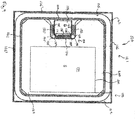
figures 9 to 11 , the semiconductor die 120 has achip layout 121 in which thegate pad 128 is positioned on thefirst surface 122 intermediate two opposingsidewalls 126, 126'. Thegate pad 128 may be positioned in approximately the centre of the distance between the twosidewalls 126, 126' and towards the periphery of athird sidewall 126" which extends between the opposingsidewalls 126, 126'. As in the embodiments illustrated infigures 1 to 8 , thegate pad 128 is positioned adjacent thecell field 124 of thesuperjunction transistor device 123 in theedge termination region 125. Thecell field 124 and the source pad 127 may have a U-shape in plan view with thegate pad 128 positioned in the open part of the U such that threesides gate pad 128 faced towards thecell field 124 and the source pad 127. - The semiconductor die 120 also includes a
gate runner 141 which laterally surrounds thecell field 124 and thegate pad 128 and includes adrain ring 142 which laterally surrounds thegate runner 141. Both thegate runner 141 and thedrain ring 142 may have a continuous ring-shaped form and are substantially concentric with the sidewalls of theupper surface 122 as in the embodiments illustrated infigures 1 to 8 . The threesides gate pad 128 are laterally surrounded by thecell field 124 due to the positioning of thegate pad 128 in approximately the centre of the distance between the opposingsidewalls 126, 126' and laterally inwards of thegate runner 141. - A
passivation layer 200 is illustrated which is positioned on at least portions of the source pad 127 and thegate pad 128 and which has anopening 201 exposing a portion of the source pad 127 which divides a contact area for producing a contact to the source pad 127. Similarly, anopening 202 is provided exposing a portion of thegate pad 128 for producing a contact area to thegate pad 128. Thepassivation layer 200 may be formed of polyimide or any combination of an imide, a nitride, an oxide or an oxynitride, for example. - Each of
figures 9 to 11 illustrates a polysiliconESD protection diode 132, 132', 132' having a differing lateral form that may be used in thechip layout 121. - The semiconductor die 120 also includes a polysilicon
ESD protection diode 132 which is positioned between thegate pad 128 and the source pad 127. Thepolysilicon protection diode 132 may also be considered to have a general U-shape in plan view. In the embodiment illustrated infigure 9 , the polysiliconESD protection diode 132 includes threeseparate sections sides gate pad 128. Thefirst section 133 and thesecond section 134 extend substantially perpendicular to one another in the top view and are separated by afirst gap 135 positioned at thefirst corner 136 of thegate pad 128 that is formed between the adjoiningwalls second section 134 is also substantially perpendicular to the third section 133' which is arranged adjacent the third side face 129' of thegate pad 128 such that a second gap 135' is formed at the second corner 136' of thegate pad 128 that is formed between thesecond side 130 and the third side 129' of thegate pad 128. The first andthird sections 133, 133' extend substantially parallel to one another and are positioned adjacent opposingsides 129, 129' of thegate pad 128. - Each of the three
sections ESD protection diode 132 has a substantially rectangular form in the top view with the long direction of the providing the width of diode. The structure of the separate threeseparate sections ESD protection diode 132 is the same as that described in connection withfigures 1 ,2 and8 . - The semiconductor die 120 also includes a shielding region, which is not illustrated in the top view of
figures 9 to 11 . The shielding region comprises a non-depletable region and a laterally contiguous depletable region as in the embodiments described with reference tofigures 1 to 8 . The shielding region surrounds thecell field 124 and has a structure and position relative to the source pad 127,gate pad 128 and polysiliconESD protection diode 132 corresponding to that described with reference tofigures 1 to 8 . In some embodiments, the gate polysilicon layer which electrically couples gate electrodes in thecell field 124 to thegate pad 128 also extends between the first andsecond sections ESD protection diode 132 through thegap 135 and under thegate pad 128 and may also extend through the second gap 135' provided at the second corner 136' and between thesecond section 134 and the third section 133' and under thegate pad 128. An integrated gate resistor may also be provided under thegate pad 128 as in the embodiments described with reference tofigures 1 to 8 . -
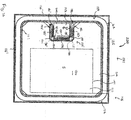
Figure 10 illustrates a top view of asemiconductor die 220 with asuperjunction transistor device 123 and with asemiconductor chip layout 221 including the arrangement of thegate pad 128, source pad 127,cell field 124,edge termination region 125,gate runner 141,drain ring 142 and shielding region described with reference to the embodiment illustrated infigure 9 . The semiconductor die 220 also includes a polysilicon ESD protection diode 132' including three laterally separatedsections sides figure 9 in the lateral form of thefirst section 133 and third section 133'. Thefirst section 133 includes afirst end 178 which is positioned at thecorner 136 and spaced apart from afirst end 180 of thesecond section 134 by thegap 135. The opposingsecond end 181 of thefirst section 133 includes acurved extension 182 which has a convex form extending away from thegate pad 128. Thecurved extension 182 is substantially concentric with the curved outer contour of the source pad 127 at this position. Similarly, the third section 133' which is substantially parallel to thefirst section 133 and positioned adjacent the opposing side face 129' of thegate pad 128 includes a first end 178' which is positioned at the second corner 136' and spaced apart from asecond end 184 of thesecond section 134 by the second gap 135' positioned at the second corner 136'. The third section 133' includes a second end 181' which includes a curved extension 182' which is convex with respect to thegate pad 128. Thesecond section 134 is substantially rectangular in plan view. The first and secondcurved extensions 182, 182' extend away from thegate pad 128 in opposing directions and may be used to increase the width of therespective section 133, 133' and, therefore, the total width of the polysilicon ESD protection diode 132'. - The shielding region which underlies the polysilicon ESD protection diode 132' and surrounds the
cell field 124 has a lateral form corresponding to the outer contour of the source pad 127 illustrated in the top view offigure 10 . Thecurved extensions 182, 182' are, therefore, positioned vertically above curved portions of the shielding region and have a lateral from corresponding to the lateral form of the shielding region so that the polysilicon ESD protection diode 132' including theextensions 182, 182' are electrically shielded from theunderlying drift region 51 and compensation region 52 (not shown in the top view offigure 10 ) by the intermediately positioned shielding region (not shown in the top view offigure 10 ) . - The opposing
sides 129, 129' of thegate pad 128 also include a curved portion that is concentric with thecurved extensions 182, 182' such that the contour of the opposingsides 129, 129' of thegate pad 128 overlaps and is positioned vertically above thecurved extensions 182, 182' of the polysilicon ESD protection diode 132'. -
Figure 11 illustrates the top view of asemiconductor die 320 with asuperjunction transistor device 123 according to another embodiment with a polysilicon ESD protection diode 132'' having a different lateral form. The polysiliconESD protection diode 132" includes a single section and comprises a firstconcave portion 385 which extends around thefirst corner 136 into a firststraight portion 333 which extends adjacent afirst side 129 of thegate pad 128 into aconvex portion 382 at adistal end 389. TheESD protection diode 132" extends in the opposing direction from thefirst corner 136 of thegate pad 128 into a second substantially straight portion 334 positioned adjacent thesecond side 130 of thegate pad 128, into a second concave portion 385' which extends around the second corner 136' of thegate pad 128 into a third substantially straight portion 333' positioned adjacent the third side 129' of thegate pad 128 which in turn extends into a second convex portion 388' at the second distal end 389'. - The use of the two
convex extension portions 388, 388' enables the width of the polysiliconESD protection diode 132" to be increased due to the more efficient occupation of the space available between thegate pad 128 and the source pad 127 and due to the use of the curved region formed between thegate pad 128 and the source pad 127 at the positions laterally adjacent the three side faces 129, 130, 129' of thegate pad 128 and the region formed between the side faces 129, 129' and thegate runner 141. - In the embodiments illustrated in
figures 9 to 11 , the semiconductor die 120, 220, 320 includes a shielding region, which is not illustrated in the top view, which has a lateral form corresponding to the outer contour of the source pad 127. The shielding region also includes curved regions between transverse and longitudinal portions of the shielding region which are concentric with the curved portions of the outer contour of the source pad 127. The polysiliconESD protection diode drift region 51 andcompensation region 52 due to the position of the polysiliconESD protection diode ESD protection diode 132, 132' is positioned above the non-depletable region of the shielding region and by forming the ESD protection diode such that it is aligned and conformal with the lateral form of the shielding region. The width of the polysilicon ESD protection diode 132' 132" can be increased in embodiments including the convex extensions compared to an arrangement including rectangular sections or rectangular distal ends whilst maintaining the electrical shielding of the polysiliconESD protection diode 132', 132" from thedrift region 51 andcompensation region 52 by extending the polysiliconESD protection diode 132', 132" over the convex portions of the shielding region. - In some embodiments, current crowding or high electrical fields within concave portions of the policy ESD protection diode are avoided by omitting concave portions at the one or more corners of the gate pad and splitting the ESD protection diode into two or three separate sections which are laterally spaced apart from one another which are electrically coupled in parallel between the source pad and the gate pad.
- In order to avoid the formation of large electric fields and current crowding effects in the curved extensions, the radius R2 of the extensions may be selected to be sufficiently large, for example R2 may be around 155 µm. In embodiments including a single polysilicon ESD diode, such as the polysilicon
ESD protection diode 32" illustrated infigure 8 or the polysiliconESD protection diode 132" illustrated infigure 11 , which have a concave radius positioned at thecorner 36; 136; 136' of thegate pad 28; 128 the radius R2 of the extensions may be larger than R1, i.e. R2 > R1 and in some embodiments, R2 > 4R1. As an example, the radius R1 of the concave portion, which is concave with respect to thegate pad 28; 128, may be around 33 µm and the radius R2 of the convex portions may be around 155 µm. - The lateral form of, and the relative positioning between, the contours of the polysilicon ESD protection diode, the curvature of the gate pad and the curvature of the source pad are selected so that they are conformal to the underlying shielding region. The polysilicon ESD protection diode is arranged on the shielding region such that it overlaps with the non-depletable region and has a lateral extent such that the depletable region extends further into the edge termination region than the polysilicon ESD protection diode. This arrangement provides electrical shielding of the polysilicon ESD protection diode by the shielding region against electrostatic and electric dynamic potentials in the drift region and compensation region below the gate pad of the semiconductor die.
- In some embodiments, the semiconductor die includes an integrated
non-depletable region 62, which extends further into theedge termination region 25 than thepolysilicon ESD diode 32. - An integrated ESD protection diode is provided for a semiconductor die including a transistor device with a smaller active area, for example a superjunction transistor device that occupies a comparably small area, as the ESD protection diode is positioned between the gate pad and the cell field and has a lateral form which is conformal to the lateral shape of the cell field, the source pad and the shielding region.
- In some embodiments, the polysilicon ESD protection diode includes convex extensions, extending away from the gate pad, that are conformal to the curvature of the shielding region in order to increase the width of the polysilicon ESD protection diode and the ESD HBM protection rating provided by the polysilicon ESD protection diode. In embodiments including two or more separate sections, the gap between neighbouring sections may be less than 10 µm, for example 2 µm or 1 µm. For example, the
gap 36 between the twosections 33, 34' may be less than 10 µm,for example 2 µm or 1 µm. The width of the polysiliconESD protection diode 32 may be extended by a corresponding amount by including the curved extensions, for example. - Spatially relative terms such as "under", "below", "lower", "over", "upper" and the like are used for ease of description to explain the positioning of one element relative to a second element. These terms are intended to encompass different orientations of the device in addition to different orientations than those depicted in the figures. Further, terms such as "first", "second", and the like, are also used to describe various elements, regions, sections, etc. and are also not intended to be limiting. Like terms refer to like elements throughout the description.
- As used herein, the terms "having", "containing", "including", "comprising" and the like are open ended terms that indicate the presence of stated elements or features, but do not preclude additional elements or features. The articles "a", "an" and "the" are intended to include the plural as well as the singular, unless the context clearly indicates otherwise. It is to be understood that the features of the various embodiments described herein may be combined with each other, unless specifically noted otherwise.
- Although specific embodiments have been illustrated and described herein, it will be appreciated by those of ordinary skill in the art that a variety of alternate and/or equivalent implementations may be substituted for the specific embodiments shown and described without departing from the scope of the present invention. This application is intended to cover any adaptations or variations of the specific embodiments discussed herein. Therefore, it is intended that this invention be limited only by the claims and the equivalents thereof.
Claims (15)
- A semiconductor die (20, 20', 20"), comprising:a transistor device (23) comprising a cell field (24) and an edge termination region (25) surrounding the cell field (24);a source pad (27) arranged on the cell field (24);a gate pad (28) arranged laterally adjacent the cell field (24) and in the edge termination region (25);a shielding region (31) laterally surrounding the cell field (24), the shielding region (31) comprising a non-depletable doped region (62);a polysilicon ESD protection diode (32);wherein the polysilicon ESD protection diode (32) is arranged laterally between the gate pad (28) and the source pad (27) and vertically above at least a portion of the shielding region (31),wherein the polysilicon ESD protection diode (32) comprises at least two separate sections (33, 34) that are electrically coupled in parallel between the gate pad (28) and the source pad (27), the sections (33, 34) being laterally spaced apart by a gap (35) situated at a corner (36) of the gate pad (28).
- The semiconductor die of claim 1, whereinthe gate pad (28) is arranged in a corner region of a first surface (22) of the semiconductor die (20) and has two adjoining sides (29, 30) surrounded by the cell field (24), wherein the polysilicon ESD protection diode (32) comprises two separate sections (33, 34) arranged adjacent the two adjoining sides (29, 30) of the gate pad (28) such that the corner (36) is arranged between the adjoining two sides (29, 30), orthe gate pad (128) is arranged on the first surface (122) intermediate two opposing sides (126, 126') of the semiconductor die (120) and has three sides (129, 130, 129') surrounded by the cell field (24), wherein the polysilicon ESD protection diode (132) comprises three separate sections (133, 134, 133') arranged adjacent the three sides (129, 130, 129') of the gate pad (128) such that the gap (135) is arranged at the corner (136) and a further gap (135') is arranged at a further corner (136') of the gate pad (128).
- The semiconductor die of claim 1 or claim 2, wherein at least one section (33, 34) of the polysilicon ESD protection diode (32) comprises a first end (78) facing towards the gap (35) and second end (81) opposing the first end (78), and the second end (81) further comprises a convex extension (82) that extends away from the gate pad (28).
- The semiconductor die of one of claims 1 to 3, further comprising a polysilicon gate connection (72) that electrically couples the gate pad (28) to gate electrodes (59) of the cell field (24), wherein the polysilicon gate connection (72) extends from under the gate pad 28), through the gap (35) to the cell field (24).
- A semiconductor die (20", 320), comprising:a transistor device (23) comprising a cell field (24) and an edge termination region (25) surrounding the cell field (24);a source pad (27) arranged on the cell field (24);a gate pad (28) arranged laterally adjacent the cell field (24) and in the edge termination region (25);a shielding region (31) laterally surrounding the cell field (24), the shielding region (31) comprising a non-depletable doped region (62);a polysilicon ESD protection diode (32");wherein the polysilicon ESD protection diode (32") is arranged laterally between the gate pad (28') and the source pad (27) and vertically above at least a portion of the shielding region (31),wherein the polysilicon ESD protection diode (32") extends along two adjoining sides (29, 30) of the gate pad (28) and comprises a concave portion (85) extending around a corner (36) of the gate pad (28) formed between the two adjoining sides (29, 30) and a convex portion (88, 89) that extends away from the gate pad (28) at each end of the polysilicon ESD protection diode (32").
- The semiconductor die of claim 5, wherein the concave portion (85) has a radius R1 and the convex portion (88, 89) has a radius R2, wherein R1 < R2.
- The semiconductor die of one of claims 1 to 6, further comprising a gate polysilicon layer (43) that electrically couples the gate pad (28) to gate electrodes (59) of the cell field (24).
- The semiconductor die of one of claims 1 to 7, further comprising a gate resistor (77) that is electrically coupled between the gate pad (28) and a gate runner (41).
- The semiconductor die of claim 8, wherein the gate resistor (77) comprises first conductive via (73) extending between a gate polysilicon layer (43) and the gate pad (28) and a second conductive via (74) extending between the gate polysilicon layer (43) and the gate runner (41).
- The semiconductor die of claim 10, wherein the gate polysilicon layer (43) comprises a gap (78) positioned laterally between the first conductive via (73) and the polysilicon ESD protection diode (32).
- The semiconductor die of one of claims 1 to 10, wherein the polysilicon ESD diode (32) comprises a plurality of doped polysilicon regions (68, 69) of opposing conductivity, wherein the regions (68, 69) of opposing conductivity are arranged alternately and laterally adjacent one another to form a plurality of vertical pn junctions, the pn junctions extending substantially concentrically to the shielding region (31).
- The semiconductor die of one of claims 1 to 11, whereinthe non-depletable region (62) of the shielding region (31) has a lateral extent such that an outermost edge of the non-depletable region (62) is positioned vertically under the polysilicon ESD protection diode (32), orthe non-depletable region (62) of the shielding region (31) has a lateral extent such that the outermost edge of the non-depletable region (62) extends further into the edge termination region than the polysilicon ESD protection diode (32), orthe shielding region (31) further comprises a depletable doped region (63) that forms a boundary (64) with the non-depletable region and the non-depletable doped region (62) of the shielding region (31) is positioned laterally adjacent the cell field (24), the depletable doped region (63) of the shielding region (31) extends into the edge termination region (25) and the polysilicon ESD protection diode (32) is positioned above the boundary (64).
- The semiconductor die of one of claims 1 to 12, wherein the non-depletable doped region (62) of the shielding region (31) comprises a doping concentration that is non-depletable by drain-source voltages applied to the transistor device (23).
- The semiconductor die (20, 120) of one of claims 1 to 13, wherein the gate pad (28) is arranged in a corner region of a first surface (22) of the semiconductor die (20) and has two adjoining sides (29, 30) surrounded by and laterally spaced apart from the source pad (27), orthe gate pad (128) is arranged on the first surface (122) intermediate two opposing sides (126, 126') of the semiconductor die (120) and has three sides (129, 130, 129') surrounded by and laterally spaced apart from the source pad (127).
- The semiconductor die of one of claims 9 to 14, further comprising an interlevel dielectric layer (61) arranged between the gate polysilicon layer (43) and the gate pad (28) and between the gate polysilicon layer (43) and the source pad (27) and/or a field oxide (67) arranged between the shielding region (31) and the gate polysilicon layer (43) and between the cell field (24) and the gate polysilicon layer (43).
Priority Applications (2)
| Application Number | Priority Date | Filing Date | Title |
|---|---|---|---|
| EP19153518.6A EP3686929B1 (en) | 2019-01-24 | 2019-01-24 | Semiconductor die |
| US16/750,958 US11430781B2 (en) | 2019-01-24 | 2020-01-23 | Semiconductor die |
Applications Claiming Priority (1)
| Application Number | Priority Date | Filing Date | Title |
|---|---|---|---|
| EP19153518.6A EP3686929B1 (en) | 2019-01-24 | 2019-01-24 | Semiconductor die |
Publications (2)
| Publication Number | Publication Date |
|---|---|
| EP3686929A1 true EP3686929A1 (en) | 2020-07-29 |
| EP3686929B1 EP3686929B1 (en) | 2023-09-20 |
Family
ID=65228466
Family Applications (1)
| Application Number | Title | Priority Date | Filing Date |
|---|---|---|---|
| EP19153518.6A Active EP3686929B1 (en) | 2019-01-24 | 2019-01-24 | Semiconductor die |
Country Status (2)
| Country | Link |
|---|---|
| US (1) | US11430781B2 (en) |
| EP (1) | EP3686929B1 (en) |
Cited By (1)
| Publication number | Priority date | Publication date | Assignee | Title |
|---|---|---|---|---|
| CN114582839A (en) * | 2022-05-06 | 2022-06-03 | 绍兴中芯集成电路制造股份有限公司 | Semiconductor device integrating ESD polysilicon layer |
Families Citing this family (5)
| Publication number | Priority date | Publication date | Assignee | Title |
|---|---|---|---|---|
| JP7234713B2 (en) * | 2019-03-14 | 2023-03-08 | 富士電機株式会社 | semiconductor equipment |
| DE102020125371B4 (en) * | 2020-09-29 | 2025-05-28 | Infineon Technologies Ag | Package with pad, which has an open cutout |
| CN113690297B (en) * | 2021-08-25 | 2023-07-28 | 厦门市三安集成电路有限公司 | Nitride device and its preparation method |
| US20240213196A1 (en) * | 2022-12-22 | 2024-06-27 | Wolfspeed, Inc. | Power Semiconductor Devices Including Multiple Layer Metallization |
| US20240355738A1 (en) * | 2023-04-21 | 2024-10-24 | Wolfspeed, Inc. | Power Semiconductor Devices Including Beryllium Metallization |
Citations (5)
| Publication number | Priority date | Publication date | Assignee | Title |
|---|---|---|---|---|
| US20080290367A1 (en) * | 2007-05-21 | 2008-11-27 | Alpha & Omega Semiconductor, Ltd | Layouts for multiple-stage ESD protection circuits for integrating with semiconductor power device |
| US20140183639A1 (en) * | 2012-12-27 | 2014-07-03 | Chengdu Monolithic Power Systems, Co., Ltd. | Esd protection structure and semiconductor device comprising the same |
| US20170271319A1 (en) * | 2016-03-15 | 2017-09-21 | Infineon Technologies Dresden Gmbh | Semiconductor Device |
| US20180090479A1 (en) | 2016-09-29 | 2018-03-29 | Infineon Technologies Dresden Gmbh | Semiconductor Devices and Methods for Forming a Semiconductor Device |
| US20180301553A1 (en) * | 2017-04-13 | 2018-10-18 | Infineon Technologies Austria Ag | Semiconductor Device Comprising a Trench Structure |
Family Cites Families (2)
| Publication number | Priority date | Publication date | Assignee | Title |
|---|---|---|---|---|
| JP6037499B2 (en) * | 2011-06-08 | 2016-12-07 | ローム株式会社 | Semiconductor device and manufacturing method thereof |
| US8466514B2 (en) * | 2011-10-17 | 2013-06-18 | Force Mos Technology Co., Ltd. | Semiconductor power device integrated with improved gate source ESD clamp diodes |
-
2019
- 2019-01-24 EP EP19153518.6A patent/EP3686929B1/en active Active
-
2020
- 2020-01-23 US US16/750,958 patent/US11430781B2/en active Active
Patent Citations (5)
| Publication number | Priority date | Publication date | Assignee | Title |
|---|---|---|---|---|
| US20080290367A1 (en) * | 2007-05-21 | 2008-11-27 | Alpha & Omega Semiconductor, Ltd | Layouts for multiple-stage ESD protection circuits for integrating with semiconductor power device |
| US20140183639A1 (en) * | 2012-12-27 | 2014-07-03 | Chengdu Monolithic Power Systems, Co., Ltd. | Esd protection structure and semiconductor device comprising the same |
| US20170271319A1 (en) * | 2016-03-15 | 2017-09-21 | Infineon Technologies Dresden Gmbh | Semiconductor Device |
| US20180090479A1 (en) | 2016-09-29 | 2018-03-29 | Infineon Technologies Dresden Gmbh | Semiconductor Devices and Methods for Forming a Semiconductor Device |
| US20180301553A1 (en) * | 2017-04-13 | 2018-10-18 | Infineon Technologies Austria Ag | Semiconductor Device Comprising a Trench Structure |
Cited By (2)
| Publication number | Priority date | Publication date | Assignee | Title |
|---|---|---|---|---|
| CN114582839A (en) * | 2022-05-06 | 2022-06-03 | 绍兴中芯集成电路制造股份有限公司 | Semiconductor device integrating ESD polysilicon layer |
| CN114582839B (en) * | 2022-05-06 | 2022-08-09 | 绍兴中芯集成电路制造股份有限公司 | Semiconductor device integrating ESD polysilicon layer |
Also Published As
| Publication number | Publication date |
|---|---|
| EP3686929B1 (en) | 2023-09-20 |
| US20200243505A1 (en) | 2020-07-30 |
| US11430781B2 (en) | 2022-08-30 |
Similar Documents
| Publication | Publication Date | Title |
|---|---|---|
| US11430781B2 (en) | Semiconductor die | |
| US11164859B2 (en) | Semiconductor device | |
| KR101654250B1 (en) | Trench-based power semiconductor devices with increased breakdown voltage characteristics | |
| KR101737593B1 (en) | Trench-based power semiconductor devices with increased breakdown voltage characteristics | |
| US6140678A (en) | Trench-gated power MOSFET with protective diode | |
| US7655975B2 (en) | Power trench transistor | |
| EP3537482B1 (en) | Semiconductor device | |
| JP5011611B2 (en) | Semiconductor device | |
| CN112216691B (en) | Semiconductor power device integrated with clamping diode | |
| US11158713B2 (en) | Semiconductor device | |
| JP2008085189A (en) | Insulated gate semiconductor device | |
| US12453139B2 (en) | Transistor device and method for producing a transistor device | |
| US20230307538A1 (en) | Transistor device | |
| US20200312969A1 (en) | Semiconductor device | |
| US12268017B2 (en) | Shielded gate trench MOSFETs with improved trench terminations and shielded gate trench contacts | |
| CN116845107A (en) | silicon carbide semiconductor components | |
| US20250040223A1 (en) | Semiconductor device | |
| JP7641156B2 (en) | Semiconductor Device | |
| JP2011009630A (en) | Protection diode | |
| JP7815134B2 (en) | Semiconductor Devices | |
| US20230038354A1 (en) | Transistor device | |
| WO2025070301A1 (en) | Semiconductor device |
Legal Events
| Date | Code | Title | Description |
|---|---|---|---|
| PUAI | Public reference made under article 153(3) epc to a published international application that has entered the european phase |
Free format text: ORIGINAL CODE: 0009012 |
|
| STAA | Information on the status of an ep patent application or granted ep patent |
Free format text: STATUS: THE APPLICATION HAS BEEN PUBLISHED |
|
| AK | Designated contracting states |
Kind code of ref document: A1 Designated state(s): AL AT BE BG CH CY CZ DE DK EE ES FI FR GB GR HR HU IE IS IT LI LT LU LV MC MK MT NL NO PL PT RO RS SE SI SK SM TR |
|
| AX | Request for extension of the european patent |
Extension state: BA ME |
|
| STAA | Information on the status of an ep patent application or granted ep patent |
Free format text: STATUS: REQUEST FOR EXAMINATION WAS MADE |
|
| 17P | Request for examination filed |
Effective date: 20210129 |
|
| RBV | Designated contracting states (corrected) |
Designated state(s): AL AT BE BG CH CY CZ DE DK EE ES FI FR GB GR HR HU IE IS IT LI LT LU LV MC MK MT NL NO PL PT RO RS SE SI SK SM TR |
|
| GRAP | Despatch of communication of intention to grant a patent |
Free format text: ORIGINAL CODE: EPIDOSNIGR1 |
|
| STAA | Information on the status of an ep patent application or granted ep patent |
Free format text: STATUS: GRANT OF PATENT IS INTENDED |
|
| RIC1 | Information provided on ipc code assigned before grant |
Ipc: H01L 29/423 20060101ALI20230316BHEP Ipc: H01L 29/06 20060101ALI20230316BHEP Ipc: H01L 29/78 20060101ALI20230316BHEP Ipc: H01L 27/02 20060101AFI20230316BHEP |
|
| INTG | Intention to grant announced |
Effective date: 20230413 |
|
| GRAS | Grant fee paid |
Free format text: ORIGINAL CODE: EPIDOSNIGR3 |
|
| GRAA | (expected) grant |
Free format text: ORIGINAL CODE: 0009210 |
|
| STAA | Information on the status of an ep patent application or granted ep patent |
Free format text: STATUS: THE PATENT HAS BEEN GRANTED |
|
| AK | Designated contracting states |
Kind code of ref document: B1 Designated state(s): AL AT BE BG CH CY CZ DE DK EE ES FI FR GB GR HR HU IE IS IT LI LT LU LV MC MK MT NL NO PL PT RO RS SE SI SK SM TR |
|
| REG | Reference to a national code |
Ref country code: GB Ref legal event code: FG4D |
|
| REG | Reference to a national code |
Ref country code: CH Ref legal event code: EP |
|
| REG | Reference to a national code |
Ref country code: DE Ref legal event code: R096 Ref document number: 602019037682 Country of ref document: DE |
|
| REG | Reference to a national code |
Ref country code: IE Ref legal event code: FG4D |
|
| P01 | Opt-out of the competence of the unified patent court (upc) registered |
Effective date: 20231114 |
|
| REG | Reference to a national code |
Ref country code: LT Ref legal event code: MG9D |
|
| PG25 | Lapsed in a contracting state [announced via postgrant information from national office to epo] |
Ref country code: GR Free format text: LAPSE BECAUSE OF FAILURE TO SUBMIT A TRANSLATION OF THE DESCRIPTION OR TO PAY THE FEE WITHIN THE PRESCRIBED TIME-LIMIT Effective date: 20231221 |
|
| REG | Reference to a national code |
Ref country code: NL Ref legal event code: MP Effective date: 20230920 |
|
| PG25 | Lapsed in a contracting state [announced via postgrant information from national office to epo] |
Ref country code: SE Free format text: LAPSE BECAUSE OF FAILURE TO SUBMIT A TRANSLATION OF THE DESCRIPTION OR TO PAY THE FEE WITHIN THE PRESCRIBED TIME-LIMIT Effective date: 20230920 Ref country code: RS Free format text: LAPSE BECAUSE OF FAILURE TO SUBMIT A TRANSLATION OF THE DESCRIPTION OR TO PAY THE FEE WITHIN THE PRESCRIBED TIME-LIMIT Effective date: 20230920 Ref country code: NO Free format text: LAPSE BECAUSE OF FAILURE TO SUBMIT A TRANSLATION OF THE DESCRIPTION OR TO PAY THE FEE WITHIN THE PRESCRIBED TIME-LIMIT Effective date: 20231220 Ref country code: LV Free format text: LAPSE BECAUSE OF FAILURE TO SUBMIT A TRANSLATION OF THE DESCRIPTION OR TO PAY THE FEE WITHIN THE PRESCRIBED TIME-LIMIT Effective date: 20230920 Ref country code: LT Free format text: LAPSE BECAUSE OF FAILURE TO SUBMIT A TRANSLATION OF THE DESCRIPTION OR TO PAY THE FEE WITHIN THE PRESCRIBED TIME-LIMIT Effective date: 20230920 Ref country code: HR Free format text: LAPSE BECAUSE OF FAILURE TO SUBMIT A TRANSLATION OF THE DESCRIPTION OR TO PAY THE FEE WITHIN THE PRESCRIBED TIME-LIMIT Effective date: 20230920 Ref country code: GR Free format text: LAPSE BECAUSE OF FAILURE TO SUBMIT A TRANSLATION OF THE DESCRIPTION OR TO PAY THE FEE WITHIN THE PRESCRIBED TIME-LIMIT Effective date: 20231221 Ref country code: FI Free format text: LAPSE BECAUSE OF FAILURE TO SUBMIT A TRANSLATION OF THE DESCRIPTION OR TO PAY THE FEE WITHIN THE PRESCRIBED TIME-LIMIT Effective date: 20230920 |
|
| REG | Reference to a national code |
Ref country code: AT Ref legal event code: MK05 Ref document number: 1614095 Country of ref document: AT Kind code of ref document: T Effective date: 20230920 |
|
| PG25 | Lapsed in a contracting state [announced via postgrant information from national office to epo] |
Ref country code: NL Free format text: LAPSE BECAUSE OF FAILURE TO SUBMIT A TRANSLATION OF THE DESCRIPTION OR TO PAY THE FEE WITHIN THE PRESCRIBED TIME-LIMIT Effective date: 20230920 |
|
| PG25 | Lapsed in a contracting state [announced via postgrant information from national office to epo] |
Ref country code: IS Free format text: LAPSE BECAUSE OF FAILURE TO SUBMIT A TRANSLATION OF THE DESCRIPTION OR TO PAY THE FEE WITHIN THE PRESCRIBED TIME-LIMIT Effective date: 20240120 |
|
| PG25 | Lapsed in a contracting state [announced via postgrant information from national office to epo] |
Ref country code: AT Free format text: LAPSE BECAUSE OF FAILURE TO SUBMIT A TRANSLATION OF THE DESCRIPTION OR TO PAY THE FEE WITHIN THE PRESCRIBED TIME-LIMIT Effective date: 20230920 |
|
| PG25 | Lapsed in a contracting state [announced via postgrant information from national office to epo] |
Ref country code: ES Free format text: LAPSE BECAUSE OF FAILURE TO SUBMIT A TRANSLATION OF THE DESCRIPTION OR TO PAY THE FEE WITHIN THE PRESCRIBED TIME-LIMIT Effective date: 20230920 |
|
| PG25 | Lapsed in a contracting state [announced via postgrant information from national office to epo] |
Ref country code: SM Free format text: LAPSE BECAUSE OF FAILURE TO SUBMIT A TRANSLATION OF THE DESCRIPTION OR TO PAY THE FEE WITHIN THE PRESCRIBED TIME-LIMIT Effective date: 20230920 Ref country code: RO Free format text: LAPSE BECAUSE OF FAILURE TO SUBMIT A TRANSLATION OF THE DESCRIPTION OR TO PAY THE FEE WITHIN THE PRESCRIBED TIME-LIMIT Effective date: 20230920 Ref country code: IS Free format text: LAPSE BECAUSE OF FAILURE TO SUBMIT A TRANSLATION OF THE DESCRIPTION OR TO PAY THE FEE WITHIN THE PRESCRIBED TIME-LIMIT Effective date: 20240120 Ref country code: ES Free format text: LAPSE BECAUSE OF FAILURE TO SUBMIT A TRANSLATION OF THE DESCRIPTION OR TO PAY THE FEE WITHIN THE PRESCRIBED TIME-LIMIT Effective date: 20230920 Ref country code: EE Free format text: LAPSE BECAUSE OF FAILURE TO SUBMIT A TRANSLATION OF THE DESCRIPTION OR TO PAY THE FEE WITHIN THE PRESCRIBED TIME-LIMIT Effective date: 20230920 Ref country code: CZ Free format text: LAPSE BECAUSE OF FAILURE TO SUBMIT A TRANSLATION OF THE DESCRIPTION OR TO PAY THE FEE WITHIN THE PRESCRIBED TIME-LIMIT Effective date: 20230920 Ref country code: AT Free format text: LAPSE BECAUSE OF FAILURE TO SUBMIT A TRANSLATION OF THE DESCRIPTION OR TO PAY THE FEE WITHIN THE PRESCRIBED TIME-LIMIT Effective date: 20230920 Ref country code: PT Free format text: LAPSE BECAUSE OF FAILURE TO SUBMIT A TRANSLATION OF THE DESCRIPTION OR TO PAY THE FEE WITHIN THE PRESCRIBED TIME-LIMIT Effective date: 20240122 Ref country code: SK Free format text: LAPSE BECAUSE OF FAILURE TO SUBMIT A TRANSLATION OF THE DESCRIPTION OR TO PAY THE FEE WITHIN THE PRESCRIBED TIME-LIMIT Effective date: 20230920 |
|
| PG25 | Lapsed in a contracting state [announced via postgrant information from national office to epo] |
Ref country code: PL Free format text: LAPSE BECAUSE OF FAILURE TO SUBMIT A TRANSLATION OF THE DESCRIPTION OR TO PAY THE FEE WITHIN THE PRESCRIBED TIME-LIMIT Effective date: 20230920 Ref country code: IT Free format text: LAPSE BECAUSE OF FAILURE TO SUBMIT A TRANSLATION OF THE DESCRIPTION OR TO PAY THE FEE WITHIN THE PRESCRIBED TIME-LIMIT Effective date: 20230920 |
|
| REG | Reference to a national code |
Ref country code: DE Ref legal event code: R097 Ref document number: 602019037682 Country of ref document: DE |
|
| PG25 | Lapsed in a contracting state [announced via postgrant information from national office to epo] |
Ref country code: DK Free format text: LAPSE BECAUSE OF FAILURE TO SUBMIT A TRANSLATION OF THE DESCRIPTION OR TO PAY THE FEE WITHIN THE PRESCRIBED TIME-LIMIT Effective date: 20230920 |
|
| PLBE | No opposition filed within time limit |
Free format text: ORIGINAL CODE: 0009261 |
|
| STAA | Information on the status of an ep patent application or granted ep patent |
Free format text: STATUS: NO OPPOSITION FILED WITHIN TIME LIMIT |
|
| PG25 | Lapsed in a contracting state [announced via postgrant information from national office to epo] |
Ref country code: DK Free format text: LAPSE BECAUSE OF FAILURE TO SUBMIT A TRANSLATION OF THE DESCRIPTION OR TO PAY THE FEE WITHIN THE PRESCRIBED TIME-LIMIT Effective date: 20230920 |
|
| PG25 | Lapsed in a contracting state [announced via postgrant information from national office to epo] |
Ref country code: MC Free format text: LAPSE BECAUSE OF FAILURE TO SUBMIT A TRANSLATION OF THE DESCRIPTION OR TO PAY THE FEE WITHIN THE PRESCRIBED TIME-LIMIT Effective date: 20230920 |
|
| 26N | No opposition filed |
Effective date: 20240621 |
|
| PG25 | Lapsed in a contracting state [announced via postgrant information from national office to epo] |
Ref country code: MC Free format text: LAPSE BECAUSE OF FAILURE TO SUBMIT A TRANSLATION OF THE DESCRIPTION OR TO PAY THE FEE WITHIN THE PRESCRIBED TIME-LIMIT Effective date: 20230920 |
|
| REG | Reference to a national code |
Ref country code: CH Ref legal event code: PL |
|
| PG25 | Lapsed in a contracting state [announced via postgrant information from national office to epo] |
Ref country code: LU Free format text: LAPSE BECAUSE OF NON-PAYMENT OF DUE FEES Effective date: 20240124 |
|
| PG25 | Lapsed in a contracting state [announced via postgrant information from national office to epo] |
Ref country code: LU Free format text: LAPSE BECAUSE OF NON-PAYMENT OF DUE FEES Effective date: 20240124 |
|
| PG25 | Lapsed in a contracting state [announced via postgrant information from national office to epo] |
Ref country code: BE Free format text: LAPSE BECAUSE OF NON-PAYMENT OF DUE FEES Effective date: 20240131 |
|
| PG25 | Lapsed in a contracting state [announced via postgrant information from national office to epo] |
Ref country code: CH Free format text: LAPSE BECAUSE OF NON-PAYMENT OF DUE FEES Effective date: 20240131 |
|
| PG25 | Lapsed in a contracting state [announced via postgrant information from national office to epo] |
Ref country code: SI Free format text: LAPSE BECAUSE OF FAILURE TO SUBMIT A TRANSLATION OF THE DESCRIPTION OR TO PAY THE FEE WITHIN THE PRESCRIBED TIME-LIMIT Effective date: 20230920 |
|
| PG25 | Lapsed in a contracting state [announced via postgrant information from national office to epo] |
Ref country code: SI Free format text: LAPSE BECAUSE OF FAILURE TO SUBMIT A TRANSLATION OF THE DESCRIPTION OR TO PAY THE FEE WITHIN THE PRESCRIBED TIME-LIMIT Effective date: 20230920 Ref country code: CH Free format text: LAPSE BECAUSE OF NON-PAYMENT OF DUE FEES Effective date: 20240131 Ref country code: BE Free format text: LAPSE BECAUSE OF NON-PAYMENT OF DUE FEES Effective date: 20240131 |
|
| REG | Reference to a national code |
Ref country code: BE Ref legal event code: MM Effective date: 20240131 |
|
| PG25 | Lapsed in a contracting state [announced via postgrant information from national office to epo] |
Ref country code: BG Free format text: LAPSE BECAUSE OF FAILURE TO SUBMIT A TRANSLATION OF THE DESCRIPTION OR TO PAY THE FEE WITHIN THE PRESCRIBED TIME-LIMIT Effective date: 20230920 |
|
| REG | Reference to a national code |
Ref country code: DE Ref legal event code: R079 Ref document number: 602019037682 Country of ref document: DE Free format text: PREVIOUS MAIN CLASS: H01L0027020000 Ipc: H10D0089000000 |
|
| PG25 | Lapsed in a contracting state [announced via postgrant information from national office to epo] |
Ref country code: BG Free format text: LAPSE BECAUSE OF FAILURE TO SUBMIT A TRANSLATION OF THE DESCRIPTION OR TO PAY THE FEE WITHIN THE PRESCRIBED TIME-LIMIT Effective date: 20230920 |
|
| PG25 | Lapsed in a contracting state [announced via postgrant information from national office to epo] |
Ref country code: IE Free format text: LAPSE BECAUSE OF NON-PAYMENT OF DUE FEES Effective date: 20240124 |
|
| PG25 | Lapsed in a contracting state [announced via postgrant information from national office to epo] |
Ref country code: IE Free format text: LAPSE BECAUSE OF NON-PAYMENT OF DUE FEES Effective date: 20240124 |
|
| PG25 | Lapsed in a contracting state [announced via postgrant information from national office to epo] |
Ref country code: CY Free format text: LAPSE BECAUSE OF FAILURE TO SUBMIT A TRANSLATION OF THE DESCRIPTION OR TO PAY THE FEE WITHIN THE PRESCRIBED TIME-LIMIT; INVALID AB INITIO Effective date: 20190124 |
|
| PG25 | Lapsed in a contracting state [announced via postgrant information from national office to epo] |
Ref country code: HU Free format text: LAPSE BECAUSE OF FAILURE TO SUBMIT A TRANSLATION OF THE DESCRIPTION OR TO PAY THE FEE WITHIN THE PRESCRIBED TIME-LIMIT; INVALID AB INITIO Effective date: 20190124 |
|
| PG25 | Lapsed in a contracting state [announced via postgrant information from national office to epo] |
Ref country code: TR Free format text: LAPSE BECAUSE OF FAILURE TO SUBMIT A TRANSLATION OF THE DESCRIPTION OR TO PAY THE FEE WITHIN THE PRESCRIBED TIME-LIMIT Effective date: 20230920 |
|
| REG | Reference to a national code |
Ref country code: DE Ref legal event code: R081 Ref document number: 602019037682 Country of ref document: DE Owner name: INFINEON TECHNOLOGIES DRESDEN AG & CO. KG, DE Free format text: FORMER OWNER: INFINEON TECHNOLOGIES DRESDEN GMBH & CO. KG, 01099 DRESDEN, DE |
|
| PGFP | Annual fee paid to national office [announced via postgrant information from national office to epo] |
Ref country code: GB Payment date: 20260123 Year of fee payment: 8 |
|
| PGFP | Annual fee paid to national office [announced via postgrant information from national office to epo] |
Ref country code: DE Payment date: 20260323 Year of fee payment: 8 |
|
| PGFP | Annual fee paid to national office [announced via postgrant information from national office to epo] |
Ref country code: FR Payment date: 20260123 Year of fee payment: 8 |