EP3686768A1 - Fingerprint recognition module and terminal device - Google Patents
Fingerprint recognition module and terminal device Download PDFInfo
- Publication number
- EP3686768A1 EP3686768A1 EP18855652.6A EP18855652A EP3686768A1 EP 3686768 A1 EP3686768 A1 EP 3686768A1 EP 18855652 A EP18855652 A EP 18855652A EP 3686768 A1 EP3686768 A1 EP 3686768A1
- Authority
- EP
- European Patent Office
- Prior art keywords
- printed circuit
- circuit board
- flexible printed
- identification module
- fingerprint identification
- Prior art date
- Legal status (The legal status is an assumption and is not a legal conclusion. Google has not performed a legal analysis and makes no representation as to the accuracy of the status listed.)
- Pending
Links
Images
Classifications
-
- G—PHYSICS
- G06—COMPUTING OR CALCULATING; COUNTING
- G06V—IMAGE OR VIDEO RECOGNITION OR UNDERSTANDING
- G06V40/00—Recognition of biometric, human-related or animal-related patterns in image or video data
- G06V40/10—Human or animal bodies, e.g. vehicle occupants or pedestrians; Body parts, e.g. hands
- G06V40/12—Fingerprints or palmprints
- G06V40/13—Sensors therefor
- G06V40/1329—Protecting the fingerprint sensor against damage caused by the finger
-
- G—PHYSICS
- G06—COMPUTING OR CALCULATING; COUNTING
- G06V—IMAGE OR VIDEO RECOGNITION OR UNDERSTANDING
- G06V40/00—Recognition of biometric, human-related or animal-related patterns in image or video data
- G06V40/10—Human or animal bodies, e.g. vehicle occupants or pedestrians; Body parts, e.g. hands
- G06V40/12—Fingerprints or palmprints
- G06V40/13—Sensors therefor
-
- G—PHYSICS
- G06—COMPUTING OR CALCULATING; COUNTING
- G06V—IMAGE OR VIDEO RECOGNITION OR UNDERSTANDING
- G06V40/00—Recognition of biometric, human-related or animal-related patterns in image or video data
- G06V40/10—Human or animal bodies, e.g. vehicle occupants or pedestrians; Body parts, e.g. hands
- G06V40/12—Fingerprints or palmprints
- G06V40/13—Sensors therefor
- G06V40/1306—Sensors therefor non-optical, e.g. ultrasonic or capacitive sensing
Definitions
- the present disclosure relates to the field of electronic technologies, in particular to a fingerprint identification module and a terminal device.
- the fingerprint identification technology has become one of the important technologies that are concerned much for the usage of terminal device.
- a fingerprint identification module is a basic part of the terminal device to realize fingerprint identification.
- electrostatic charges may enter through the gap in usage. Since there is no low impedance path in the fingerprint identification module to conduct away the electrostatic charges, the electrostatic charges are prone to be conducted directly to a bottom side of a fingerprint chip and discharged to the fingerprint chip, thereby causing damage to the fingerprint chip.
- a fingerprint identification module is provided in the embodiments of the present disclosure.
- the fingerprint identification module is applied to a terminal device and includes: a decorative ring, provided with a mounting opening; an encapsulation cover, arranged on the decorative ring to close a side of the mounting opening; a fingerprint chip, disposed in the mounting opening, where a space is formed between an outer side surface of the fingerprint chip and an inner wall surface of the decorative ring; a protective film, disposed on a side of the fingerprint chip that is towards the encapsulation cover; a flexible printed circuit board, disposed inside the mounting opening, where the protective film covers a first partial area of the flexible printed circuit board, a second partial area of the flexible printed circuit board is exposed out of the protective film; the second partial area is an area of the flexible printed circuit board which is different from the first partial area of the flexible printed circuit board.
- a terminal device is further provided in the embodiments of the present disclosure.
- the terminal device includes the fingerprint identification module described above.
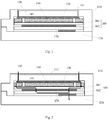
- FIG. 1 a schematic structural diagram of a fingerprint identification module according to an embodiment of the present disclosure is illustrated.
- a fingerprint identification module is applied to a terminal device.
- the fingerprint identification module may include: a decorative ring 110, provided with a mounting opening 111; an encapsulation cover 120, arranged on the decorative ring 110 to close a side of the mounting opening 111; a fingerprint chip 130, disposed in the mounting opening 111, where a space is formed between an outer side surface of the fingerprint chip 130 and an inner wall surface of the decorative ring 110; a protective film 150, disposed on a side of the fingerprint chip 130 that is towards the encapsulation cover 120; a flexible printed circuit board 140, disposed inside the mounting opening 111, where the protective film 150 covers a first partial area of the flexible printed circuit board 140, a second partial area of the flexible printed circuit board 140 is exposed out of the protective film 150; the second partial area is an area of the flexible printed circuit board which is different from the first partial area of the flexible printed circuit board 140.
- the encapsulation cover 120 may be a shielding cover configured to shield against external electromagnetic interference and protect the fingerprint identification module.
- the encapsulation cover 120 may further be configured to discharge electrostatic charges.
- the flexible printed circuit board 140 is electrically connected to the fingerprint chip 130. A distance between the flexible printed circuit board 140 and the encapsulation cover 120 is smaller than a distance between the fingerprint chip 130 and the encapsulation cover 120. Wirings are disposed concentratedly in the first partial area of the flexible printed circuit board 140, and the protective film 150 is disposed between the fingerprint chip 130 and the flexible printed circuit board 140 to cover the first partial area, thereby providing insulation protection to the first partial area.
- FIG. 2 a schematic diagram illustrating an electrostatic discharge path in a fingerprint identification module according to an embodiment of the present disclosure is illustrated.
- a path from the space, the second partial area of the flexible printed circuit board 140 to the encapsulation cover 120 forms the electrostatic discharge path.
- electrostatic charges enter via the space between the outer side surface of the fingerprint chip 130 and the inner wall surface of the decorative ring 110, and then a low-impedance path provided by using the second partial area of the flexible printed circuit board 140 enables the electrostatic charges to be conducted to the encapsulation cover 120 via the second partial area and discharged.
- the second partial area of the flexible printed circuit board 140 is used to provide the low-impedance path to form the electrostatic discharge path in the fingerprint identification module, so as to discharge the electrostatic charges having entered the fingerprint identification module, thereby preventing the electrostatic charges from damaging the fingerprinting chip, and improving the reliability of the fingerprint identification module.
- the first partial area corresponds to a middle area of the flexible printed circuit board 140, and the second partial area surrounds the first partial area.
- the electrostatic discharge path is formed by a path from the space, the second partial area of the flexible printed circuit board 140 to the encapsulation cover 120, which may conduct most of the entered electrostatic charges to the encapsulation cover 120.
- the electrostatic discharge path is formed by a path from the space, the second partial area of the flexible printed circuit board 140 to the encapsulation cover 120, which may conduct most of the entered electrostatic charges to the encapsulation cover 120.
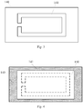
- a slot 141 passing through two opposite surfaces of the flexible printed circuit board 140 is provided in the flexible printed circuit board 140.
- the slot 141 provided in the flexible printed circuit board 140 is configured to form a gap on the flexible printed circuit board 140, so as to block the electrostatic charges flowing through the second partial area of the flexible printed circuit board 140 from being conducted to the fingerprint chip 130 via the copper foil of the flexible printed circuit board 140.
- the slot 141 has a semi-closed annular structure in one embodiment, as shown in Fig. 3 and Fig. 4 .
- the flexible printed circuit board 140 is partially separated by the slot 141 having the semi-closed annular structure, and the electrostatic charges flowing through the flexible printed circuit board 140 are blocked out of the middle area of the flexible printed circuit board 140 where the wirings are concentrated by using the gap formed by the slot 141 in the flexible printed circuit board 140, thereby preventing the electrostatic charges from being conducted to the fingerprint chip 130 via the flexible printed circuit board 140 and causing damage to the fingerprint chip 130.
- the protective film 150 covers an opening of the slot 141 that is towards the fingerprint chip 130, to increase an impedance difference between two parts of the flexible printed circuit board 140 which are separated by the slot 141, thereby preventing the electrostatic charges from jumping to the middle area of the flexible printed circuit board 140 via the gap formed by the slot 141 in the flexible printed circuit board 140.
- the fingerprint identification module may further include: a reinforcing steel sheet 160 disposed between the flexible printed circuit board 140 and the encapsulation cover 120.
- the reinforcing steel sheet 160 is snugly attached to the flexible printed circuit board 140, so as to, on one hand, support the flexible printed circuit board 140, thereby improving the strength of an plug-in position on the flexible printed circuit board 140 to facilitate the overall product assembly, and on the other hand, serve as a ground connection.
- grounding may be achieved by connecting to a main ground of the terminal device via the reinforcing steel sheet 160.
- an electrically conductive foam 170 is disposed between the encapsulation cover 120 and the reinforcing steel sheet 160.
- the encapsulation cover 120 is connected to the reinforcing steel sheet 160 by the electrically conductive foam 170 which may not only serve as a cushion for protection, but also function as an electric conductor, so that the electrostatic charges flowing through the reinforcing steel sheet 160 may be conducted to the encapsulation cover 120.
- the reinforcing steel sheet 160 includes a first steel sheet 161 and a second steel sheet 162.
- the first steel sheet 161 is snugly attached to a side of the flexible printed circuit board 140 that is away from the fingerprint chip 130, and the second steel sheet 162 is disposed on a side of the first steel sheet 161 that is away from the flexible printed circuit board 140.
- the first steel sheet 161 is mainly configured to support the flexible printed circuit board 140 to improve the strength of the plug-in position on the flexible printed circuit board 140, thereby facilitating the overall product assembly.
- the second steel sheet 162 is configured to be connected to a ground of the motherboard of the terminal device, that is, be connected to the main ground.
- the electrically conductive foam 170 is disposed between the first steel sheet 161 and the second steel sheet 162.
- the first steel sheet 161 is electrically connected to the second steel sheet 162 via the conductive steel sheet 170 which may double as a cushion for protection.
- the fingerprint chip 130 may be encapsulated by using a Land Grid Array (LGA) technology.
- LGA Land Grid Array
- the electrostatic discharge path is formed from the space between the outer side surface of the fingerprint chip and the inner wall surface of the decorative ring, the second partial area of the flexible printed circuit board uncovered by the protective film to the encapsulation cover, thereby discharging the electrostatic charges having entered the fingerprint identification module, which prevents the electrostatic charges from damaging the fingerprinting chip and improves the reliability of the fingerprint identification module.
- a terminal device is further provided in an embodiments of the present disclosure.
- the terminal device includes the fingerprint identification module described above.
- the structure of the main body of the terminal device is the same as or similar to that in the related art, and the structure and principle of the fingerprint identification module are described in detail in the above embodiments, a description of the specific structure of the terminal device is omitted in this embodiment.
- the terminal device may be a mobile phone, a tablet computer, a laptop computer or a personal digital assistant (PDA), etc.
- PDA personal digital assistant
- the electrostatic discharge path is formed in the fingerprint identification module, the electrostatic charges having entered the fingerprint identification module are conducted and discharged, which may solve the problem of the related art that the fingerprint chip is prone to be damaged by the entered electrostatic charges during usage of the fingerprint identification module. Therefore, the reliability, stability and comfortability of the terminal device may be improved, and the user experience is improved.
- a term such as “include” or “including” is used to indicate the presence of enumerated features or components, but does not exclude the presence of one or more other enumerated features or one or more other components.
- a term “mounted”, “connected”, “attached”, “fixed”, “disposed” or the like should be understood in a broad sense unless otherwise specified and defined, for example, it may be a fixed connection, a detachable connection or a integration; it may be a mechanical connection or an electrical connection; it may be a direct connection, or it may be an indirect connection via an intermediate medium, or it may refer to an internal connection between two components or an interaction between two components.
- the specific meanings of the above term in the present disclosure may be understood according to specific contexts.
- a relational term such as first and second is only used to distinguish one entity or operation from another entity or operation, and does not necessarily require or imply that there is such an actual relationship or order between these entities or operations.
Landscapes
- Engineering & Computer Science (AREA)
- Human Computer Interaction (AREA)
- Physics & Mathematics (AREA)
- General Physics & Mathematics (AREA)
- Multimedia (AREA)
- Theoretical Computer Science (AREA)
- Shielding Devices Or Components To Electric Or Magnetic Fields (AREA)
- Telephone Set Structure (AREA)
- Image Input (AREA)
- Measurement Of Length, Angles, Or The Like Using Electric Or Magnetic Means (AREA)
- Measurement Of The Respiration, Hearing Ability, Form, And Blood Characteristics Of Living Organisms (AREA)
- Casings For Electric Apparatus (AREA)
- Elimination Of Static Electricity (AREA)
Abstract
Description
- This application claims a priority to Chinese Patent Application No.
201710841562.2 - The present disclosure relates to the field of electronic technologies, in particular to a fingerprint identification module and a terminal device.
- With the rapid development of electronic technologies, users have an increasing demand for terminal devices, and have higher requirements for user experience of the terminal devices. With the continuous development and application of a fingerprint identification technology on the terminal device, the fingerprint identification technology has become one of the important technologies that are concerned much for the usage of terminal device.
- A fingerprint identification module is a basic part of the terminal device to realize fingerprint identification. In the related art, due to a gap between the fingerprint identification module and a decorative ring, electrostatic charges may enter through the gap in usage. Since there is no low impedance path in the fingerprint identification module to conduct away the electrostatic charges, the electrostatic charges are prone to be conducted directly to a bottom side of a fingerprint chip and discharged to the fingerprint chip, thereby causing damage to the fingerprint chip.
- A fingerprint identification module is provided in the embodiments of the present disclosure. The fingerprint identification module is applied to a terminal device and includes: a decorative ring, provided with a mounting opening; an encapsulation cover, arranged on the decorative ring to close a side of the mounting opening; a fingerprint chip, disposed in the mounting opening, where a space is formed between an outer side surface of the fingerprint chip and an inner wall surface of the decorative ring; a protective film, disposed on a side of the fingerprint chip that is towards the encapsulation cover; a flexible printed circuit board, disposed inside the mounting opening, where the protective film covers a first partial area of the flexible printed circuit board, a second partial area of the flexible printed circuit board is exposed out of the protective film; the second partial area is an area of the flexible printed circuit board which is different from the first partial area of the flexible printed circuit board.
- A terminal device is further provided in the embodiments of the present disclosure. The terminal device includes the fingerprint identification module described above.
- In order to illustrate the technical solutions of the embodiments of the present disclosure in a clearer manner, the drawings required for the description of the embodiments of the present disclosure will be introduced hereinafter briefly. Obviously, the following drawings merely illustrate some embodiments of the present disclosure, and based on these drawings, a person of ordinary skill in the art may obtain other drawings without any creative effort.
-
Fig. 1 is a schematic structural diagram of a fingerprint identification module according to an embodiment of the present disclosure; -
Fig. 2 is a schematic diagram illustrating an electrostatic discharge path in a fingerprint identification module according to an embodiment of the present disclosure; -
Fig. 3 is a schematic structural diagram of a flexible printed circuit board in a fingerprint identification module according to an embodiment of the present disclosure; -
Fig. 4 is a schematic assembly diagram of a flexible printed circuit board and a protective film according to an embodiment of the present disclosure. - In order to make the technical problem to be solved, the technical solution and advantages of the present disclosure clearer, a detailed description will be given below with reference to the accompanying drawings and specific embodiments.
- Referring to
Fig. 1 , a schematic structural diagram of a fingerprint identification module according to an embodiment of the present disclosure is illustrated. - A fingerprint identification module is applied to a terminal device. The fingerprint identification module may include: a
decorative ring 110, provided with amounting opening 111; anencapsulation cover 120, arranged on thedecorative ring 110 to close a side of themounting opening 111; afingerprint chip 130, disposed in themounting opening 111, where a space is formed between an outer side surface of thefingerprint chip 130 and an inner wall surface of thedecorative ring 110; aprotective film 150, disposed on a side of thefingerprint chip 130 that is towards theencapsulation cover 120; a flexible printedcircuit board 140, disposed inside themounting opening 111, where theprotective film 150 covers a first partial area of the flexible printedcircuit board 140, a second partial area of the flexible printedcircuit board 140 is exposed out of theprotective film 150; the second partial area is an area of the flexible printed circuit board which is different from the first partial area of the flexible printedcircuit board 140. - In some embodiments of the present disclosure, the
encapsulation cover 120 may be a shielding cover configured to shield against external electromagnetic interference and protect the fingerprint identification module. In addition, theencapsulation cover 120 may further be configured to discharge electrostatic charges. The flexible printedcircuit board 140 is electrically connected to thefingerprint chip 130. A distance between the flexible printedcircuit board 140 and theencapsulation cover 120 is smaller than a distance between thefingerprint chip 130 and theencapsulation cover 120. Wirings are disposed concentratedly in the first partial area of the flexible printedcircuit board 140, and theprotective film 150 is disposed between thefingerprint chip 130 and the flexible printedcircuit board 140 to cover the first partial area, thereby providing insulation protection to the first partial area. - Referring to
Fig. 2 , a schematic diagram illustrating an electrostatic discharge path in a fingerprint identification module according to an embodiment of the present disclosure is illustrated. In this embodiment, a path from the space, the second partial area of the flexible printedcircuit board 140 to theencapsulation cover 120 forms the electrostatic discharge path. Specifically, electrostatic charges enter via the space between the outer side surface of thefingerprint chip 130 and the inner wall surface of thedecorative ring 110, and then a low-impedance path provided by using the second partial area of the flexible printedcircuit board 140 enables the electrostatic charges to be conducted to theencapsulation cover 120 via the second partial area and discharged. - In this embodiment, the second partial area of the flexible printed
circuit board 140 is used to provide the low-impedance path to form the electrostatic discharge path in the fingerprint identification module, so as to discharge the electrostatic charges having entered the fingerprint identification module, thereby preventing the electrostatic charges from damaging the fingerprinting chip, and improving the reliability of the fingerprint identification module. - In some embodiments, the first partial area corresponds to a middle area of the flexible printed
circuit board 140, and the second partial area surrounds the first partial area. - In this embodiment, the electrostatic discharge path is formed by a path from the space, the second partial area of the flexible printed
circuit board 140 to theencapsulation cover 120, which may conduct most of the entered electrostatic charges to theencapsulation cover 120. However, considering that there is an electrical connection between a copper foil of the flexible printedcircuit board 140 and thefingerprint chip 130, in order to avoid a situation that a small amount of the electrostatic charges may be conducted to thefingerprint chip 130 via the copper foil of the flexible printedcircuit board 140 when the electrostatic charges having entered via the space are conducted to the second partial area of the flexible printedcircuit board 140, in an embodiment, as shown inFig. 1 andFig. 3 , aslot 141 passing through two opposite surfaces of the flexible printedcircuit board 140 is provided in the flexible printedcircuit board 140. In this embodiment, theslot 141 provided in the flexible printedcircuit board 140 is configured to form a gap on the flexible printedcircuit board 140, so as to block the electrostatic charges flowing through the second partial area of the flexible printedcircuit board 140 from being conducted to thefingerprint chip 130 via the copper foil of the flexible printedcircuit board 140. - In this embodiment, considering a circuit design characteristic of the flexible printed
circuit board 140 in the fingerprint identification module, i.e., the wirings of the flexible printedcircuit board 140 are disposed concentratedly in the middle area, theslot 141 has a semi-closed annular structure in one embodiment, as shown inFig. 3 and Fig. 4 . In this embodiment, the flexible printedcircuit board 140 is partially separated by theslot 141 having the semi-closed annular structure, and the electrostatic charges flowing through the flexible printedcircuit board 140 are blocked out of the middle area of the flexible printedcircuit board 140 where the wirings are concentrated by using the gap formed by theslot 141 in the flexible printedcircuit board 140, thereby preventing the electrostatic charges from being conducted to thefingerprint chip 130 via the flexible printedcircuit board 140 and causing damage to thefingerprint chip 130. - Referring to
Fig. 1 andFig. 4 , in one embodiment, theprotective film 150 covers an opening of theslot 141 that is towards thefingerprint chip 130, to increase an impedance difference between two parts of the flexible printedcircuit board 140 which are separated by theslot 141, thereby preventing the electrostatic charges from jumping to the middle area of the flexible printedcircuit board 140 via the gap formed by theslot 141 in the flexible printedcircuit board 140. - Referring to
Fig. 1 , in one embodiment, the fingerprint identification module may further include: a reinforcingsteel sheet 160 disposed between the flexible printedcircuit board 140 and theencapsulation cover 120. In this embodiment, the reinforcingsteel sheet 160 is snugly attached to the flexible printedcircuit board 140, so as to, on one hand, support the flexible printedcircuit board 140, thereby improving the strength of an plug-in position on the flexible printedcircuit board 140 to facilitate the overall product assembly, and on the other hand, serve as a ground connection. Specifically, grounding may be achieved by connecting to a main ground of the terminal device via the reinforcingsteel sheet 160. - Referring to
Fig. 1 , in one embodiment, an electricallyconductive foam 170 is disposed between theencapsulation cover 120 and the reinforcingsteel sheet 160. In this embodiment, theencapsulation cover 120 is connected to the reinforcingsteel sheet 160 by the electricallyconductive foam 170 which may not only serve as a cushion for protection, but also function as an electric conductor, so that the electrostatic charges flowing through the reinforcingsteel sheet 160 may be conducted to theencapsulation cover 120. - Referring to
Fig. 1 , in one embodiment, the reinforcingsteel sheet 160 includes afirst steel sheet 161 and asecond steel sheet 162. Thefirst steel sheet 161 is snugly attached to a side of the flexible printedcircuit board 140 that is away from thefingerprint chip 130, and thesecond steel sheet 162 is disposed on a side of thefirst steel sheet 161 that is away from the flexible printedcircuit board 140. In this embodiment, thefirst steel sheet 161 is mainly configured to support the flexible printedcircuit board 140 to improve the strength of the plug-in position on the flexible printedcircuit board 140, thereby facilitating the overall product assembly. Thesecond steel sheet 162 is configured to be connected to a ground of the motherboard of the terminal device, that is, be connected to the main ground. - Specifically, in one embodiment, the electrically
conductive foam 170 is disposed between thefirst steel sheet 161 and thesecond steel sheet 162. In this embodiment, thefirst steel sheet 161 is electrically connected to thesecond steel sheet 162 via theconductive steel sheet 170 which may double as a cushion for protection. - In the embodiment of the present disclosure, the
fingerprint chip 130 may be encapsulated by using a Land Grid Array (LGA) technology. - In the fingerprint identification module according to the embodiment of the present disclosure, the electrostatic discharge path is formed from the space between the outer side surface of the fingerprint chip and the inner wall surface of the decorative ring, the second partial area of the flexible printed circuit board uncovered by the protective film to the encapsulation cover, thereby discharging the electrostatic charges having entered the fingerprint identification module, which prevents the electrostatic charges from damaging the fingerprinting chip and improves the reliability of the fingerprint identification module.
- A terminal device is further provided in an embodiments of the present disclosure. The terminal device includes the fingerprint identification module described above.
- Since the structure of the main body of the terminal device is the same as or similar to that in the related art, and the structure and principle of the fingerprint identification module are described in detail in the above embodiments, a description of the specific structure of the terminal device is omitted in this embodiment.
- In addition, the terminal device may be a mobile phone, a tablet computer, a laptop computer or a personal digital assistant (PDA), etc.
- According to the terminal device with the fingerprint identification module in the embodiment of the present disclosure, since the electrostatic discharge path is formed in the fingerprint identification module, the electrostatic charges having entered the fingerprint identification module are conducted and discharged, which may solve the problem of the related art that the fingerprint chip is prone to be damaged by the entered electrostatic charges during usage of the fingerprint identification module. Therefore, the reliability, stability and comfortability of the terminal device may be improved, and the user experience is improved.
- It is understood, "an embodiment", "one embodiment" or "some embodiments" mentioned throughout the specification means specific features, structures or characteristics related to the embodiment are included in at least one embodiment or example of the present disclosure. Therefore, "in an embodiment", "in one embodiment" or "in some embodiments" mentioned throughout the specification does not necessarily refer to the same embodiment. In addition, elements, structures, or features described in one drawing or one embodiment of the present disclosure may be combined with elements, structures, or features shown in one or more other drawings or embodiments in any suitable manner.
- In addition, in one or more embodiments of the present disclosure, a term such as "include" or "including" is used to indicate the presence of enumerated features or components, but does not exclude the presence of one or more other enumerated features or one or more other components.
- In the present disclosure, a term "mounted", "connected", "attached", "fixed", "disposed" or the like should be understood in a broad sense unless otherwise specified and defined, for example, it may be a fixed connection, a detachable connection or a integration; it may be a mechanical connection or an electrical connection; it may be a direct connection, or it may be an indirect connection via an intermediate medium, or it may refer to an internal connection between two components or an interaction between two components. For a person of ordinary skill in the art, the specific meanings of the above term in the present disclosure may be understood according to specific contexts.
- In addition, in the embodiments of the present disclosure, a relational term such as first and second is only used to distinguish one entity or operation from another entity or operation, and does not necessarily require or imply that there is such an actual relationship or order between these entities or operations.
- The above are merely optional implementations of the present disclosure, it should be appreciated that a person of ordinary skill in the art may make further modifications and improvements without departing from the principle of the present disclosure, and these modifications and improvements shall also fall within the scope of the present disclosure.
Claims (10)
- A fingerprint identification module, applied to a terminal device, comprising:a decorative ring, provided with a mounting opening;an encapsulation cover, arranged on the decorative ring to close a side of the mounting opening;a fingerprint chip, disposed in the mounting opening, wherein a space is formed between an outer side surface of the fingerprint chip and an inner wall surface of the decorative ring;a protective film, disposed on a side of the fingerprint chip that is towards the encapsulation cover;a flexible printed circuit board, disposed inside the mounting opening, wherein the protective film covers a first partial area of the flexible printed circuit board, a second partial area of the flexible printed circuit board is exposed out of the protective film; the second partial area is an area of the flexible printed circuit board which is different from the first partial area of the flexible printed circuit board.
- The fingerprint identification module according to claim 1, wherein the first partial area corresponds to a middle area of the flexible printed circuit board, the second partial area surrounds the first partial area.
- The fingerprint identification module according to claim 1, wherein the flexible printed circuit board is provided with a slot passing through two opposite surfaces of the flexible printed circuit board.
- The fingerprint identification module according to claim 3, wherein the slot has a semi-closed annular structure.
- The fingerprint identification module according to claim 3, wherein the protective film covers an opening of the slot that is towards the fingerprint chip.
- The fingerprint identification module according to claim 1, further comprising:
a reinforcing steel sheet, disposed between the flexible printed circuit board and the encapsulation cover. - The fingerprint identification module according to claim 6, wherein an electrically conductive foam is disposed between the encapsulation cover and the reinforcing steel sheet.
- The fingerprint identification module according to claim 6, wherein the reinforcing steel sheet comprises a first steel sheet and a second steel sheet, the first steel sheet is snugly attached to a side of the flexible printed circuit board that is away from the fingerprint chip, the second steel sheet is disposed on a side of the first steel sheet that is away from the flexible printed circuit board.
- The fingerprint identification module according to claim 8, wherein an electrically conductive foam is disposed between the first steel sheet and the second steel sheet.
- A terminal device, comprising the fingerprint identification module according to any one of claims 1 to 9.
Applications Claiming Priority (2)
| Application Number | Priority Date | Filing Date | Title |
|---|---|---|---|
| CN201710841562.2A CN107665335B (en) | 2017-09-18 | 2017-09-18 | Fingerprint identification module and terminal equipment |
| PCT/CN2018/102698 WO2019052333A1 (en) | 2017-09-18 | 2018-08-28 | Fingerprint recognition module and terminal device |
Publications (2)
| Publication Number | Publication Date |
|---|---|
| EP3686768A1 true EP3686768A1 (en) | 2020-07-29 |
| EP3686768A4 EP3686768A4 (en) | 2020-11-18 |
Family
ID=61097392
Family Applications (1)
| Application Number | Title | Priority Date | Filing Date |
|---|---|---|---|
| EP18855652.6A Pending EP3686768A4 (en) | 2017-09-18 | 2018-08-28 | FINGERPRINT RECOGNITION MODULE AND TERMINAL DEVICE |
Country Status (4)
| Country | Link |
|---|---|
| US (1) | US11157718B2 (en) |
| EP (1) | EP3686768A4 (en) |
| CN (1) | CN107665335B (en) |
| WO (1) | WO2019052333A1 (en) |
Families Citing this family (13)
| Publication number | Priority date | Publication date | Assignee | Title |
|---|---|---|---|---|
| CN107665335B (en) | 2017-09-18 | 2020-06-12 | 维沃移动通信有限公司 | Fingerprint identification module and terminal equipment |
| CN110175543B (en) * | 2019-05-14 | 2023-04-07 | 上海摩软通讯技术有限公司 | Fingerprint module and fingerprint module device |
| CN110866516B (en) * | 2019-11-25 | 2022-12-27 | 维沃移动通信有限公司 | Electronic device |
| CN111144339B (en) * | 2019-12-30 | 2023-03-24 | 业泓科技(成都)有限公司 | Fingerprint identification module and electronic device |
| CN111126351B (en) * | 2020-01-21 | 2024-02-09 | 北京京东方光电科技有限公司 | Fingerprint recognition module |
| KR102958348B1 (en) * | 2020-06-23 | 2026-04-30 | 삼성디스플레이 주식회사 | Display device |
| CN111914776B (en) * | 2020-08-07 | 2023-12-22 | 业泓科技(成都)有限公司 | display device |
| CN112232112A (en) * | 2020-09-03 | 2021-01-15 | 江西合力泰科技有限公司 | Fingerprint module with strong antistatic property |
| CN112580533B (en) * | 2020-12-23 | 2022-11-18 | 天津网安技术有限公司 | A fingerprint authentication device for identity authentication |
| CN113065390A (en) * | 2021-02-03 | 2021-07-02 | 深圳阜时科技有限公司 | Narrow strip-shaped fingerprint chip, side-edge type fingerprint chip module and electronic equipment |
| CN113328234B (en) * | 2021-05-31 | 2022-12-23 | 青岛海信移动通信技术股份有限公司 | Mobile terminal |
| WO2023159608A1 (en) | 2022-02-28 | 2023-08-31 | 京东方科技集团股份有限公司 | Pattern recognition module and pattern recognition apparatus |
| WO2026035033A1 (en) * | 2024-08-07 | 2026-02-12 | 삼성전자 주식회사 | Electronic device including fingerprint sensor |
Family Cites Families (20)
| Publication number | Priority date | Publication date | Assignee | Title |
|---|---|---|---|---|
| US6067368A (en) | 1996-01-26 | 2000-05-23 | Authentec, Inc. | Fingerprint sensor having filtering and power conserving features and related methods |
| JP2003148906A (en) | 2001-11-13 | 2003-05-21 | Toko Inc | Capacitive sensor device |
| JP2010186807A (en) * | 2009-02-10 | 2010-08-26 | Sumitomo Electric Printed Circuit Inc | Flexible printed wiring board, and release sheet body |
| TW201316895A (en) * | 2011-10-14 | 2013-04-16 | Hon Hai Prec Ind Co Ltd | Printed circuit board capable of preventing electromagnetic interface |
| JP2013229505A (en) * | 2012-04-26 | 2013-11-07 | Sharp Corp | Flexible printed circuit board, display device, and electronic apparatus |
| US9030440B2 (en) | 2012-05-18 | 2015-05-12 | Apple Inc. | Capacitive sensor packaging |
| US10036734B2 (en) * | 2013-06-03 | 2018-07-31 | Snaptrack, Inc. | Ultrasonic sensor with bonded piezoelectric layer |
| CN104038866A (en) * | 2014-06-30 | 2014-09-10 | 青岛歌尔声学科技有限公司 | Circuit board with static protection function and Bluetooth earphone |
| CN104077572B (en) * | 2014-07-02 | 2018-07-31 | 南昌欧菲生物识别技术有限公司 | Fingerprint recognition detection components and terminal device |
| CN105046190B (en) * | 2015-05-08 | 2017-12-19 | 苏州迈瑞微电子有限公司 | Fingerprint recognition module |
| US9760754B2 (en) * | 2015-07-06 | 2017-09-12 | Sunasic Technologies Inc. | Printed circuit board assembly forming enhanced fingerprint module |
| TWM523147U (en) | 2015-09-10 | 2016-06-01 | 茂丞科技股份有限公司 | Fingerprint sensing unit and fingerprint sensing module |
| CN205318405U (en) * | 2015-11-20 | 2016-06-15 | 维沃移动通信有限公司 | Fingerprint identification module and terminal equipment |
| CN106022253A (en) | 2016-05-17 | 2016-10-12 | 深圳天珑无线科技有限公司 | Mobile terminal and fingerprint module group thereof |
| CN206178867U (en) | 2016-08-16 | 2017-05-17 | 广东欧珀移动通信有限公司 | Fingerprint module and have its mobile terminal |
| WO2018032870A1 (en) * | 2016-08-16 | 2018-02-22 | 广东欧珀移动通信有限公司 | Fingerprint module and mobile terminal having same |
| CN106657478B (en) * | 2017-01-20 | 2020-03-03 | Oppo广东移动通信有限公司 | Fingerprint identification module and mobile terminal |
| CN206353806U (en) | 2017-01-20 | 2017-07-25 | 广东欧珀移动通信有限公司 | Fingerprint module and mobile terminal |
| CN206388201U (en) | 2017-01-20 | 2017-08-08 | 广东欧珀移动通信有限公司 | Fingerprint module and mobile terminal |
| CN107665335B (en) | 2017-09-18 | 2020-06-12 | 维沃移动通信有限公司 | Fingerprint identification module and terminal equipment |
-
2017
- 2017-09-18 CN CN201710841562.2A patent/CN107665335B/en active Active
-
2018
- 2018-08-28 US US16/648,350 patent/US11157718B2/en active Active
- 2018-08-28 EP EP18855652.6A patent/EP3686768A4/en active Pending
- 2018-08-28 WO PCT/CN2018/102698 patent/WO2019052333A1/en not_active Ceased
Also Published As
| Publication number | Publication date |
|---|---|
| WO2019052333A1 (en) | 2019-03-21 |
| CN107665335B (en) | 2020-06-12 |
| US11157718B2 (en) | 2021-10-26 |
| CN107665335A (en) | 2018-02-06 |
| EP3686768A4 (en) | 2020-11-18 |
| US20200218877A1 (en) | 2020-07-09 |
Similar Documents
| Publication | Publication Date | Title |
|---|---|---|
| US11157718B2 (en) | Fingerprint identification module and terminal device | |
| CN107403995B (en) | Electronic device | |
| CN108141995B (en) | Connector combination structure of electronic equipment and portable electronic device having same | |
| US9843128B2 (en) | Waterproof electrical connector | |
| US20150303561A1 (en) | Modular antenna for near field coupling integration into metallic chassis devices | |
| CN108633170B (en) | Printed circuit board assembly and electronic equipment | |
| US10922513B2 (en) | Electronic component and electronic device comprising same | |
| EP3001649B1 (en) | Mobile terminal | |
| CN108604750B (en) | Clip-type current contactor and protective device including the same | |
| WO2017162136A1 (en) | Antenna apparatus, metal housing and mobile terminal | |
| US20140334119A1 (en) | Anti-emi shielding assembly and electronic device using the same | |
| JPWO2018211791A1 (en) | Portable electronic devices | |
| EP4156881B1 (en) | Shielding cover, circuit board assembly and electronic device | |
| CN104144598B (en) | Radome and circuit board fixation structure | |
| CN105827753A (en) | Portable user terminal, protection sleeve applied to same and assembly part | |
| CN202635004U (en) | Electromagnetic shielding structure applied to electronic equipment | |
| CN107819192A (en) | Back plate | |
| KR20160004786A (en) | Semiconductor package module | |
| US11158932B2 (en) | Full screen electronic device and antenna thereof | |
| US11659649B2 (en) | Electronic device | |
| JP2009059615A (en) | Connector and information processing apparatus | |
| CN206401510U (en) | Antenna device and electronic equipment | |
| US20180159212A1 (en) | Device assembly applied to mobile terminal and mobile terminal | |
| CN107484403A (en) | Shields, circuit board assemblies, and electronic devices | |
| US8140130B2 (en) | Electronic device provided with a battery unit |
Legal Events
| Date | Code | Title | Description |
|---|---|---|---|
| STAA | Information on the status of an ep patent application or granted ep patent |
Free format text: STATUS: THE INTERNATIONAL PUBLICATION HAS BEEN MADE |
|
| PUAI | Public reference made under article 153(3) epc to a published international application that has entered the european phase |
Free format text: ORIGINAL CODE: 0009012 |
|
| STAA | Information on the status of an ep patent application or granted ep patent |
Free format text: STATUS: REQUEST FOR EXAMINATION WAS MADE |
|
| 17P | Request for examination filed |
Effective date: 20200313 |
|
| AK | Designated contracting states |
Kind code of ref document: A1 Designated state(s): AL AT BE BG CH CY CZ DE DK EE ES FI FR GB GR HR HU IE IS IT LI LT LU LV MC MK MT NL NO PL PT RO RS SE SI SK SM TR |
|
| AX | Request for extension of the european patent |
Extension state: BA ME |
|
| A4 | Supplementary search report drawn up and despatched |
Effective date: 20201016 |
|
| RIC1 | Information provided on ipc code assigned before grant |
Ipc: G06K 9/20 20060101ALI20201012BHEP Ipc: G06K 9/00 20060101AFI20201012BHEP |
|
| DAV | Request for validation of the european patent (deleted) | ||
| DAX | Request for extension of the european patent (deleted) | ||
| STAA | Information on the status of an ep patent application or granted ep patent |
Free format text: STATUS: EXAMINATION IS IN PROGRESS |
|
| 17Q | First examination report despatched |
Effective date: 20221121 |