EP3683843A1 - Organic light emitting display device and method of manufacturing the same - Google Patents
Organic light emitting display device and method of manufacturing the same Download PDFInfo
- Publication number
- EP3683843A1 EP3683843A1 EP20152067.3A EP20152067A EP3683843A1 EP 3683843 A1 EP3683843 A1 EP 3683843A1 EP 20152067 A EP20152067 A EP 20152067A EP 3683843 A1 EP3683843 A1 EP 3683843A1
- Authority
- EP
- European Patent Office
- Prior art keywords
- opening
- layer
- pixel
- emission layer
- pixel electrode
- Prior art date
- Legal status (The legal status is an assumption and is not a legal conclusion. Google has not performed a legal analysis and makes no representation as to the accuracy of the status listed.)
- Granted
Links
Images





Classifications
-
- H—ELECTRICITY
- H10—SEMICONDUCTOR DEVICES; ELECTRIC SOLID-STATE DEVICES NOT OTHERWISE PROVIDED FOR
- H10K—ORGANIC ELECTRIC SOLID-STATE DEVICES
- H10K50/00—Organic light-emitting devices
- H10K50/10—OLEDs or polymer light-emitting diodes [PLED]
- H10K50/17—Carrier injection layers
-
- H—ELECTRICITY
- H10—SEMICONDUCTOR DEVICES; ELECTRIC SOLID-STATE DEVICES NOT OTHERWISE PROVIDED FOR
- H10K—ORGANIC ELECTRIC SOLID-STATE DEVICES
- H10K59/00—Integrated devices, or assemblies of multiple devices, comprising at least one organic light-emitting element covered by group H10K50/00
- H10K59/10—OLED displays
- H10K59/12—Active-matrix OLED [AMOLED] displays
- H10K59/122—Pixel-defining structures or layers, e.g. banks
-
- H—ELECTRICITY
- H10—SEMICONDUCTOR DEVICES; ELECTRIC SOLID-STATE DEVICES NOT OTHERWISE PROVIDED FOR
- H10K—ORGANIC ELECTRIC SOLID-STATE DEVICES
- H10K50/00—Organic light-emitting devices
- H10K50/10—OLEDs or polymer light-emitting diodes [PLED]
- H10K50/11—OLEDs or polymer light-emitting diodes [PLED] characterised by the electroluminescent [EL] layers
- H10K50/125—OLEDs or polymer light-emitting diodes [PLED] characterised by the electroluminescent [EL] layers specially adapted for multicolour light emission, e.g. for emitting white light
-
- H—ELECTRICITY
- H10—SEMICONDUCTOR DEVICES; ELECTRIC SOLID-STATE DEVICES NOT OTHERWISE PROVIDED FOR
- H10K—ORGANIC ELECTRIC SOLID-STATE DEVICES
- H10K50/00—Organic light-emitting devices
- H10K50/10—OLEDs or polymer light-emitting diodes [PLED]
- H10K50/14—Carrier transporting layers
- H10K50/15—Hole transporting layers
-
- H—ELECTRICITY
- H10—SEMICONDUCTOR DEVICES; ELECTRIC SOLID-STATE DEVICES NOT OTHERWISE PROVIDED FOR
- H10K—ORGANIC ELECTRIC SOLID-STATE DEVICES
- H10K50/00—Organic light-emitting devices
- H10K50/10—OLEDs or polymer light-emitting diodes [PLED]
- H10K50/14—Carrier transporting layers
- H10K50/16—Electron transporting layers
-
- H—ELECTRICITY
- H10—SEMICONDUCTOR DEVICES; ELECTRIC SOLID-STATE DEVICES NOT OTHERWISE PROVIDED FOR
- H10K—ORGANIC ELECTRIC SOLID-STATE DEVICES
- H10K50/00—Organic light-emitting devices
- H10K50/80—Constructional details
- H10K50/84—Passivation; Containers; Encapsulations
- H10K50/842—Containers
- H10K50/8428—Vertical spacers, e.g. arranged between the sealing arrangement and the OLED
-
- H—ELECTRICITY
- H10—SEMICONDUCTOR DEVICES; ELECTRIC SOLID-STATE DEVICES NOT OTHERWISE PROVIDED FOR
- H10K—ORGANIC ELECTRIC SOLID-STATE DEVICES
- H10K59/00—Integrated devices, or assemblies of multiple devices, comprising at least one organic light-emitting element covered by group H10K50/00
- H10K59/10—OLED displays
- H10K59/12—Active-matrix OLED [AMOLED] displays
- H10K59/124—Insulating layers formed between TFT elements and OLED elements
-
- H—ELECTRICITY
- H10—SEMICONDUCTOR DEVICES; ELECTRIC SOLID-STATE DEVICES NOT OTHERWISE PROVIDED FOR
- H10K—ORGANIC ELECTRIC SOLID-STATE DEVICES
- H10K59/00—Integrated devices, or assemblies of multiple devices, comprising at least one organic light-emitting element covered by group H10K50/00
- H10K59/30—Devices specially adapted for multicolour light emission
- H10K59/35—Devices specially adapted for multicolour light emission comprising red-green-blue [RGB] subpixels
-
- H—ELECTRICITY
- H10—SEMICONDUCTOR DEVICES; ELECTRIC SOLID-STATE DEVICES NOT OTHERWISE PROVIDED FOR
- H10K—ORGANIC ELECTRIC SOLID-STATE DEVICES
- H10K59/00—Integrated devices, or assemblies of multiple devices, comprising at least one organic light-emitting element covered by group H10K50/00
- H10K59/30—Devices specially adapted for multicolour light emission
- H10K59/35—Devices specially adapted for multicolour light emission comprising red-green-blue [RGB] subpixels
- H10K59/353—Devices specially adapted for multicolour light emission comprising red-green-blue [RGB] subpixels characterised by the geometrical arrangement of the RGB subpixels
-
- H—ELECTRICITY
- H10—SEMICONDUCTOR DEVICES; ELECTRIC SOLID-STATE DEVICES NOT OTHERWISE PROVIDED FOR
- H10K—ORGANIC ELECTRIC SOLID-STATE DEVICES
- H10K59/00—Integrated devices, or assemblies of multiple devices, comprising at least one organic light-emitting element covered by group H10K50/00
- H10K59/80—Constructional details
- H10K59/84—Parallel electrical configurations of multiple OLEDs
-
- H—ELECTRICITY
- H10—SEMICONDUCTOR DEVICES; ELECTRIC SOLID-STATE DEVICES NOT OTHERWISE PROVIDED FOR
- H10K—ORGANIC ELECTRIC SOLID-STATE DEVICES
- H10K59/00—Integrated devices, or assemblies of multiple devices, comprising at least one organic light-emitting element covered by group H10K50/00
- H10K59/80—Constructional details
- H10K59/88—Dummy elements, i.e. elements having non-functional features
-
- H—ELECTRICITY
- H10—SEMICONDUCTOR DEVICES; ELECTRIC SOLID-STATE DEVICES NOT OTHERWISE PROVIDED FOR
- H10K—ORGANIC ELECTRIC SOLID-STATE DEVICES
- H10K71/00—Manufacture or treatment specially adapted for the organic devices covered by this subclass
-
- H—ELECTRICITY
- H10—SEMICONDUCTOR DEVICES; ELECTRIC SOLID-STATE DEVICES NOT OTHERWISE PROVIDED FOR
- H10K—ORGANIC ELECTRIC SOLID-STATE DEVICES
- H10K59/00—Integrated devices, or assemblies of multiple devices, comprising at least one organic light-emitting element covered by group H10K50/00
- H10K59/10—OLED displays
- H10K59/12—Active-matrix OLED [AMOLED] displays
- H10K59/1201—Manufacture or treatment
-
- H—ELECTRICITY
- H10—SEMICONDUCTOR DEVICES; ELECTRIC SOLID-STATE DEVICES NOT OTHERWISE PROVIDED FOR
- H10K—ORGANIC ELECTRIC SOLID-STATE DEVICES
- H10K59/00—Integrated devices, or assemblies of multiple devices, comprising at least one organic light-emitting element covered by group H10K50/00
- H10K59/10—OLED displays
- H10K59/12—Active-matrix OLED [AMOLED] displays
- H10K59/121—Active-matrix OLED [AMOLED] displays characterised by the geometry or disposition of pixel elements
-
- H—ELECTRICITY
- H10—SEMICONDUCTOR DEVICES; ELECTRIC SOLID-STATE DEVICES NOT OTHERWISE PROVIDED FOR
- H10K—ORGANIC ELECTRIC SOLID-STATE DEVICES
- H10K59/00—Integrated devices, or assemblies of multiple devices, comprising at least one organic light-emitting element covered by group H10K50/00
- H10K59/30—Devices specially adapted for multicolour light emission
- H10K59/35—Devices specially adapted for multicolour light emission comprising red-green-blue [RGB] subpixels
- H10K59/352—Devices specially adapted for multicolour light emission comprising red-green-blue [RGB] subpixels the areas of the RGB subpixels being different
Definitions
- the technical field relates to an organic light emitting display device and a method of manufacturing an organic light emitting display device.
- OLED devices are self-luminous display devices that use organic light emitting diodes to emit light to display images.
- An OLED device does not require a separate light source; thus, the thickness and weight of the OLED device can be minimized.
- An OLED device may include a plurality of pixels. If electric charges undesirably flow from one pixel (of a certain color) into another pixel (of another color) during operation of the OLED device, the quality of images displayed by the OLED device may be unsatisfactory.
- Embodiments may be related to an organic light emitting display (OLED) device in which lateral leakage current between pixels may be minimized.
- OLED organic light emitting display
- Embodiments may be related to a method of manufacturing the OLED device.
- An OLED device may include the following elements: a substrate including a first pixel area, a second pixel area, a third pixel area, and a peripheral area surrounding the first to third pixel areas; a first pixel electrode, a second pixel electrode, and a third pixel electrode disposed on the substrate, the first pixel electrode, the second pixel electrode, and the third pixel electrode respectively overlapping the first pixel area, the second pixel area, and the third pixel area; a pixel defining layer disposed on the substrate, the pixel defining layer overlapping the peripheral area and having an upper surface at which an uneven structure is formed between the first pixel area and the second pixel area; a hole injection layer disposed on the first to third pixel electrodes and the pixel defining layer, the hole injection layer being formed along a profile of the upper surface of the pixel defining layer; a first emission layer, a second emission layer, and a third emission layer disposed on the hole injection layer, the first emission layer, the second emission layer, and the third emission
- the uneven structure may be formed only between the first pixel area and the second pixel area.
- the upper surface of the pixel defining layer between the first pixel area and the third pixel area may be flat.
- a distance between the first pixel area and the second pixel area may be less than a distance between the first pixel area and the third pixel area.
- the uneven structure may be further formed at the upper surface of the pixel defining layer between the first pixel area and the third pixel area.
- a portion of the upper surface of the pixel defining layer at which the uneven structure is not formed may be flat.
- the second pixel area may be located in a first direction from the first pixel area, and the uneven structure may include concave portions and convex portions alternatively arranged along the first direction.
- each of the concave portions may extend in a second direction perpendicular to the first direction and parallel to the substrate.
- lengths of the concave portions may be uniform.
- lengths of the concave portions may increase as being away from the first pixel area or the second pixel area.
- the OLED device may further include a spacer disposed between the pixel defining layer and the hole injection layer, the spacer overlapping the peripheral area and not overlapping the uneven structure.
- the first emission layer, the second emission layer, and the third emission layer may respectively emit a red light, a green light, and a blue light.
- the OLED device may further include a hole transport layer disposed between the hole injection layer and the first to third emission layers, the hole transport layer being formed along a profile of the upper surface of the pixel defining layer.
- the OLED device may further include an electron transport layer disposed between the first to third emission layers and the common electrode, the electron transport layer being formed along a profile of the upper surface of the pixel defining layer.
- An OLED device may include the following elements: a plurality of pixels each including a pixel electrode, a hole injection layer, an emission layer, and a common electrode which are sequentially stacked; and a pixel defining layer dividing the plurality of pixels, the pixel defining layer having an upper surface at which an uneven structure is formed between the plurality of pixels.
- the hole injection layer may be formed commonly over the plurality of pixels and along a profile of the upper surface of the pixel defining layer.
- a portion of the upper surface of the pixel defining layer at which the uneven structure is not formed may be flat.
- the uneven structure may include concave portions and convex portions alternatively arranged between the plurality of pixels.
- a method of manufacturing an OLED device may include the following steps: forming a first pixel electrode, a second pixel electrode, and a third pixel electrode on the substrate, the first pixel electrode, the second pixel electrode, and the third pixel electrode respectively overlapping the first pixel area, the second pixel area, and the third pixel area; forming a pixel defining layer on the substrate, the pixel defining layer overlapping a peripheral area surrounding the first to third pixel areas and having an upper surface at which an uneven structure is formed between the first pixel area and the second pixel area; forming a hole injection layer on the first to third pixel electrodes and the pixel defining layer, the hole injection layer being formed along a profile of the upper surface of the pixel defining layer; forming a first emission layer, a second emission layer, and a third emission layer on the hole injection layer, the first emission layer, the second emission layer, and the third emission layer respectively overlapping the first pixel area, the second pixel area, and the third pixel area; and forming
- the second pixel area may be located in a first direction from the first pixel area, and the uneven structure may include concave portions and convex portions alternatively arranged along the first direction.
- forming the pixel defining layer may include forming a preliminary pixel defining layer on the substrate on which the first to third pixel electrodes are formed, providing a halftone mask over the preliminary pixel defining layer, and exposing and developing the preliminary pixel defining layer using the halftone mask.
- the halftone mask may include light transmitting portions, light shielding portions, and semi-light transmitting portions.
- the light transmitting portions may correspond to opening portions of the pixel defining layer respectively exposing the first to third pixel electrodes
- the light shielding portions may correspond to the convex portions of the uneven structure
- the semi-light transmitting portions may correspond to the concave portions of the uneven structure.
- An embodiment may be related to an organic light emitting display (OLED) device.
- the OLED device may include the following elements: a substrate; a first pixel electrode, a second pixel electrode, and a third pixel electrode each overlapping the substrate; a pixel defining layer including a first opening, a second opening, and a third opening respectively partially exposing the first pixel electrode, the second pixel electrode, and the third pixel electrode, wherein the pixel defining layer may include a first uneven surface and a first flat face, wherein the first uneven surface may be opposite the first flat face and may be positioned between the first opening and the second opening, and wherein the first flat face may be positioned between the first pixel electrode and the second pixel electrode and may be positioned between the first uneven surface and the substrate; a first emission layer, a second emission layer, and a third emission layer respectively corresponding to the first opening, the second opening, and the third opening; and a common electrode overlapping each of the first emission layer, the second emission layer, and the third emission layer.
- the first uneven surface may be only positioned between the first emission layer and the second emission layer.
- the first uneven surface may be positioned between two opposite parallel faces of the first emission layer.
- a surface of the pixel defining layer may be positioned not farther from the common electrode than any other surfaces of the pixel defining layer, may be positioned between the first opening and the third opening, and may be flat.
- a minimum distance between the first emission layer and the second emission layer may be less than a minimum distance between the first emission layer and the third emission layer.
- the pixel defining layer may include a second uneven surface and a second flat face.
- the second uneven surface may be positioned between the first opening and the third opening and may be opposite the second flat face.
- the second flat face may be positioned between the first pixel electrode and the third pixel electrode and may be positioned between the second uneven surface and the substrate.
- a surface of the pixel defining layer may be positioned not farther from the common electrode than any other surfaces of the pixel defining layer, may be positioned between the second opening and the third opening, and may be flat.
- the first uneven surface may include cavities and protrusions alternatively arranged between the first opening and the second opening.
- a lengthwise direction of each of the cavities may be parallel to an edge of the first opening and may be parallel to the substrate.
- Lengths of the cavities may be equal.
- the cavities include a first cavity and a second cavity.
- the first cavity may be positioned closer to the first opening than the second cavity and may be shorter than the second cavity.
- the OLED device may include the following elements: a hole injection layer directly contacting each of the first pixel electrode, the second pixel electrode, the third pixel electrode, and the pixel defining layer; and a spacer disposed between the pixel defining layer and the hole injection layer and directly contacting a second flat face of the pixel defining layer.
- the hole injection layer may include cavities. The cavities may be positioned between the first opening and the second opening.
- the second flat face of the pixel defining layer may extend from an edge of the second opening to an edge of the third opening and may be spaced from the first uneven surface.
- the first emission layer, the second emission layer, and the third emission layer may be respectively configured to emit a red light, a green light, and a blue light.
- the first emission layer and the second emission layer may immediately neighbor each other with no intervening emission layer between the first emission layer and the second emission layer.
- the OLED device may include the following elements: a hole injection layer directly contacting each of the first pixel electrode, the second pixel electrode, the third pixel electrode, and the pixel defining layer; and a hole transport layer disposed between the hole injection layer and each of the first emission layer, the second emission layer, and the third emission layer.
- the hole transport layer may overlap the pixel defining layer and may include cavities. The cavities may be positioned between the first opening and the second opening.
- the OLED device may include an electron transport layer disposed between the common electrode and each of the first emission layer, the second emission layer, and the third emission layer, the electron transport layer overlapping the pixel defining layer.
- An embodiment may be related to an OLED device.
- the OLED device may include the following elements: a common electrode; a first pixel electrode overlapping the common electrode; a first emission layer positioned between the first pixel electrode and the common electrode; a second pixel electrode; a second emission layer positioned between the second pixel electrode and the common electrode; and a pixel defining layer including a first opening, a second opening, a first flat face, and an uneven surface structure, wherein the first opening partially exposes the first pixel electrode, wherein the second opening partially exposes the second pixel electrode, wherein the first flat face may be opposite the uneven surface, may be positioned between the first pixel electrode and the second pixel electrode, and may extend from the first pixel electrode to the second pixel electrode, and wherein the uneven surface may be positioned between the fist opening and the second opening.
- the OLED device may include the following elements: a third pixel electrode; and a third emission layer positioned between the third pixel electrode and the common electrode.
- the pixel defining layer may include a third opening, a second flat face, and a third flat face.
- the third opening may partially expose the third pixel electrode.
- the second flat face may be opposite the third flat face, may be positioned between the second pixel electrode and the third pixel electrode, and may extend from the second pixel electrode to the third pixel electrode.
- the third flat face may be positioned between the second opening and the third opening and may extend from the second opening to the third opening.
- the uneven surface may include cavities and protrusions alternatively arranged between the first opening and the second opening.
- An embodiment may be related to a method of manufacturing an OLED device.
- the method may include the following steps: forming a first pixel electrode, a second pixel electrode, and a third pixel electrode on a substrate; forming a pixel defining layer on the substrate, wherein the pixel defining layer may include a first opening, a second opening, and a third opening respectively partially exposing the first pixel electrode, the second pixel electrode, and the third pixel electrode, wherein the pixel defining layer may include an uneven surface and a first flat face, wherein the uneven surface may be opposite the first flat face and may be positioned between the first opening and the second opening, and wherein the first flat face may be positioned between the first pixel electrode and the second pixel electrode and may be positioned between the uneven surface and the substrate; forming a first emission layer, a second emission layer, and a third emission layer that respectively correspond to the first opening, the second opening, and the third opening; and forming a common electrode that overlaps each of the first emission layer, the second emission
- the uneven surface may include cavities and protrusions alternatively arranged between the first opening and the second opening.
- Forming the pixel defining layer may include the following steps: forming a material layer on the substrate, the first pixel electrode, the second pixel electrode, and the third pixel electrode; providing a halftone mask over the material layer; and exposing and developing the material layer using the halftone mask.
- the halftone mask may include light transmitting portions, light shielding portions, and semi-light transmitting portions.
- the light transmitting portions may correspond to the first opening, the second opening, and the third opening.
- the light shielding portions may correspond to the protrusions of the uneven surface structure.
- the semi-light transmitting portions may correspond to the cavities of the uneven surface structure.
- An OLED device may include a pixel defining layer having an upper surface with an uneven structure between pixels, and a hole injection layer may be formed on the pixel defining layer. Accordingly, an electrical path of the hole injection layer between the pixels may lengthen, and lateral leakage current between the pixels through the hole injection layer may decrease.
- the pixel defining layer may be formed using a halftone mask so that the pixel defining layer having opening portions and an uneven upper surface may be formed by single photolithography process. Therefore, manufacturing time and/or cost of the OLED device may be minimized.
- an OLED device as set out in claim 1. Additional features are set out in claims 2 to 13. According to an aspect, there is provided a method as set out in claim 14. Additional features are set out in claim 15.
- first,” “second,” etc. may be used to describe various elements, these elements, should not be limited by these terms. These terms may be used to distinguish one element from another element. A first element may be termed a second element without departing from teachings of one or more embodiments. The description of an element as a “first” element may not require or imply the presence of a second element or other elements. The terms “first,” “second,” etc. may be used to differentiate different categories or sets of elements. For conciseness, the terms “first,” “second,” etc. may represent “first-type (or first-set),” “second-type (or second-set),” etc., respectively.
- FIG. 1 is a plan view illustrating an OLED according to an embodiment.
- FIG. 2 is a cross-sectional view taken along a line II-II' in FIG. 1 according to an embodiment.
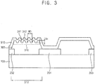
- FIG. 3 is a cross-sectional view illustrating a pixel defining layer and a hole injection layer in FIG. 2 according to an embodiment.
- the OLED device may include a substrate 100, a plurality of pixel electrodes 201, 202, and 203, a pixel defining layer 300; a spacer 400, a hole injection layer 510, a hole transport layer 520, a plurality of emission layers 531, 532, and 533; an electron transport layer 540, and a common electrode 600.
- the OLED device may include a plurality of pixels PX1, PX2, and PX3 defined by the plurality of pixel electrodes 201, 202, and 203, the hole injection layer 510, the hole transport layer 520, the plurality of emission layers 531, 532, and 533, the electron transport layer 540, and the common electrode 600. Boundaries of the pixels and/or boundaries of pixel areas associated with the pixels may correspond to edges of openings of the pixel defining layer 300.
- the substrate 100 may be substantially formed of transparent glass containing SiO x .
- the substrate 100 may be formed of a plastic material.
- the substrate 100 may include at least one thin film transistor and/or a capacitor for driving each pixel; a circuit for driving the pixel may use the thin film transistor, the capacitor, and the like.
- the substrate 100 may include a plurality of pixel areas PXA1, PXA2, and PXA3 and a peripheral area PPA.
- the pixel areas PXA1, PXA2, and PXA3 may include a plurality of first pixel areas PXA1, a plurality of second pixel areas PXA2, and a plurality of third pixel areas PXA3.
- a first pixel area PXA1, a second pixel area PXA2, and a third pixel area PXA3 may be spaced apart from each other.
- the third pixel area PXA3 may be spaced from the second pixel area PXA2 in a second direction DR2 perpendicular to the first direction DR1.
- the third pixel area PXA3 may be spaced from the second pixel area PXA2 in the first direction DR1.
- the third pixel area PXA3 may be spaced from the first pixel area PXA1 in a third direction DR3 or in a fourth direction DR4 perpendicular to the third direction DR3.
- the third direction DR3 may be inclined by about 45 degrees in a clockwise direction from the first direction DR1
- the fourth direction DR4 may be inclined by about 45 degrees in a clockwise direction from the second direction DR2.
- Boundaries of the pixel areas PXA1, PXA2, and PXA3 may respectively correspond to (bottom) boundaries of openings OP1, OP2, and OP3 of the pixel defining layer 300.
- a distance between the first pixel area PXA1 and the second pixel area PXA2 is less than a distance between the first pixel area PXA1 and the third pixel area PXA3.
- a distance D12 between the first pixel area PXA1 and the second pixel area PXA2 may be about 19.2 ⁇ m
- a distance D13 between the first pixel area PXA1 and the third pixel area PXA3 may be about 25.9 ⁇ m.
- the peripheral area PPA may surround the pixel areas PXA1, PXA2, and PXA3.
- the pixel electrodes 201, 202, and 203 may be disposed on the substrate 100.
- the pixel electrodes 201, 202, and 203 may include a first pixel electrode 201, a second pixel electrode 202, and a third pixel electrode 203.
- the first pixel electrode 201, the second pixel electrode 202, and the third pixel electrode 203 may overlap the first pixel area PXA1, the second pixel area PXA2, and the third pixel area PXA3, respectively.
- the first to third pixel electrodes 201, 202, and 203 may include at least one of a reflective conductive material, a transparent conductive material, a semi-transparent conductive material, etc.
- the pixel defining layer 300 may be disposed on the substrate 100.
- the pixel defining layer 300 may include a plurality of opening portions OP1, OP2, and OP3 (or openings OP1, OP2, and OP3).
- the opening portions OP1, OP2, and OP3 may include a first opening portion OP1, a second opening portion OP2, and a third opening portion OP3.
- the first opening portion OP1, the second opening portion OP2, and the third opening portion OP3 may expose the first pixel electrode 201, the second pixel electrode 202, and the third pixel electrode 203, respectively.
- the first to third opening portions OP1, OP2, and OP3 may respectively cover edge portions of the first to third pixel electrodes 201, 202, and 203, and may respectively expose central portions of the first to third pixel electrodes 201, 202, and 203.
- the pixel defining layer 300 may overlap the peripheral area PPA.
- the opening portions OP1, OP2, and OP3 may define the pixels PX1, PX2, and PX3, respectively.
- the pixel defining layer 300 may divide the pixels PX1, PX2, and PX3 from each other.
- the pixel defining layer 300 may include a photosensitive organic insulation material.
- the pixels PX1, PX2, and PX3 may include a first pixel PX1, a second pixel PX2, and a third pixel PX3 emitting different colors of light.
- the first pixel PX1, the second pixel PX2, and the third pixel PX3 may be a red pixel emitting red light, a green pixel emitting green light, and a blue pixel emitting blue light, respectively.
- Each of the pixels PX1, PX2, and PX3 may include one of the pixel electrode 201, 202, and 203, a portion of the hole injection layer 510, a portion of the hole transport layer 520, one of the emission layer 531, 532, and 533, a portion of the electron transport layer 540, and a portion of the common electrode 600.
- An uneven structure 310 may be formed at an upper surface of the pixel defining layer 300.
- the uneven structure 310 may be formed between the pixels PX1, PX2, and PX3.
- one or more uneven structures 310 may be formed between the first pixel area PXA1 and other pixel areas PXA2 and PXA3.
- one or more uneven structures 310 may be formed between the first pixel area PXA1 and the second pixel area PXA2 and/or between the first pixel area PXA1 and the third pixel area PXA3.
- an uneven structure 310 may also be formed between the second pixel area PXA2 and the third pixel area PXA3.
- An upper surface of the pixel defining layer 300 at which no uneven structure 310 is formed may be substantially flat (or planarized).
- the uneven structure 310 may be formed only between the first pixel area PXA1 and the second pixel area PXA2, and no uneven structure 310 may be formed between the first pixel area PXA1 and the third pixel area PXA3.
- an upper surface of the pixel defining layer 300 between the first pixel area PXA1 and the third pixel area PXA3 may be substantially flat (or planarized).
- the uneven structure 310 may include a plurality of concave portions 311 (or cavities 311) and a plurality of convex portions 312 (or protrusions 312).
- the concave portions 311 may be recessed from the upper surface of the pixel defining layer 300 toward the substrate 100, and the convex portions 312 may protrude toward the common electrode 600.
- the concave portions 311 and the convex portions 312 may be alternatively arranged along the first direction DR1 or the second direction DR2 in which the second pixel area PXA2 is spaced from the first pixel area PXA1.
- the uneven structure 310 may have a predetermined thickness TH.
- the thickness TH of the uneven structure 310 may be about 1.4 ⁇ m.
- the thickness TH of the uneven structure 310 may correspond to a depth of the concave portion 311 of the uneven structure 310.
- the uneven structure 310 may include uneven units periodically formed by the concave portions 311 and the convex portions 312 which are alternatively arranged, and the uneven unit may have a predetermined width WD.
- the width WD of the uneven unit may be about 2.9 ⁇ m.
- the width WD of the uneven unit may correspond to a sum of a width of the concave portion 311 and a width of the convex portion 312.
- an electrical path length of the upper surface of the pixel defining layer 300 which is defined along the concave portions 311 and the convex portions 312 of the uneven structure 310 may increase.
- Each of the concave portions 311 may extend along a direction perpendicular to a direction along which the concave portions 311 and the convex portions 312 are alternatively arranged and parallel to the substrate 100.
- each of the concave portions 311 may extend in the second direction DR2 and may extend perpendicular to the nearest edges of the openings of the pixel defining layer 300; the lengthwise directions of the concave portions 311 may be the second direction DR2.
- each of the concave portions 311 may extend in the first direction DR1; the lengthwise directions of the concave portions 311 may be the first direction DR1.
- lengths L1 of the concave portions 311 may be substantially equal to one another.
- the length L1 of the concave portion 311 may be a length in a lengthwise direction of the concave portion 311.
- the concave portions 311 may have substantially the same lengths L1.
- Spacers 400 may be disposed on the pixel defining layer 300.
- a spacer 400 may overlap the peripheral area PPA.
- the spacer 400 may not overlap the uneven structure 310.
- No spacer 400 may be formed between the first pixel area PXA1 and other pixel areas PXA2 and PXA3.
- the spacer 400 may support an encapsulation substrate, an encapsulation layer, etc. formed over the pixels PX1, PX2, and PX3, and may separate the encapsulation substrate, the encapsulation layer, etc. from the pixels PX1, PX2, and PX3 to protect the pixels PX1, PX2, and PX3.
- the spacer 400 may include a photosensitive organic insulation material.
- the spacer 400 may include substantially the same material as that of the pixel defining layer 300 and may be significantly wider than each concave portion 311, each convex portion 312, multiple concave portions 311, and/or multiple convex portions 312 in a width direction of each concave portion 311 or each convex portion 312.
- the hole injection layer 510 may be disposed on the first to third pixel electrodes 201, 202, and 203, the pixel defining layer 300, and the spacer 400.
- the hole injection layer 510 may be commonly formed over the first to third pixels PX1, PX2, and PX3.
- the hole injection layer 510 may be located over an entire upper surface of the substrate 100.
- the hole injection layer 510 may serve to improve the injection of holes from each of the pixel electrodes 201, 202, and 203 to the hole transport layer 520.
- the hole injection layer 510 may include one or more phthalocyanine compounds such as at least one of copper phthalocyanine, polyaniline/dodecylbenzenesulfonic acid (PANI/DBSA), 4,4',4"-tris ⁇ N,-(2-naphthyl)-N-phenylamino ⁇ -triphenylamine (2TNATA), 4,4',4"-tris(3-methylphenylphenylamino)triphenylamine (m-MTDATA), 4,4'4"-Tris(N,N-diphenylamino)triphenylamine (TDATA), polyaniline/camphor sulfonic acid (PANI/CSA), polyaniline/poly(4-styrenesulfonate) (PANI/PSS), N,N-diphenyl-N,
- the hole injection layer 510 may be formed along profiles of the first to third pixel electrodes 201, 202, and 203 and the pixel defining layer 300 on the substrate 100.
- the hole injection layer 510 may be formed along a profile of the upper surface of the pixel defining layer 300.
- the hole injection layer 510 may be formed along a profile of the uneven structure 310 formed at the upper surface of the pixel defining layer 300 between the first pixel area PXA1 and the second pixel area PXA2. Further, the hole injection layer 510 may be formed along a profile of the substantially flat (or planarized) upper surface of the pixel defining layer 300 between the first pixel area PXA1 and the third pixel area PXA3.
- a length of the hole injection layer 510 between the first pixel area PXA1 and the second pixel area PXA2 may increase.
- a horizontal distance D12 between the first pixel area PXA1 and the second pixel area PXA2 is about 19.2 ⁇ m
- a length of the hole injection layer 510 between the first pixel area PXA1 and the second pixel area PXA2 may be about 21.5 ⁇ m.
- the uneven structure 310 is formed at the upper surface of the pixel defining layer 300 between the first pixel area PXA1 and the second pixel area PXA2, such that a length of the hole injection layer 510 between the first pixel area PXA1 and the second pixel area PXA2 may be about 28.0 ⁇ m. Therefore, when the uneven structure 310 is formed at the upper surface of the pixel defining layer 300, the length of the hole injection layer 510 may increase by about 1.3 times.
- the hole injection layer 510 may be formed of a material having a relatively high charge mobility. When formed as a common layer over the pixels PX1, PX2, and PX3, the hole injection layer 510 may become a path for the movement of electric charges (holes) between the pixels PX1, PX2, and PX3. Accordingly, when one pixel is driven, lateral leakage current may flow through an adjacent pixel via the hole injection layer 510 if the hole injection layer 510 provides a sufficiently short electrical path.
- the p represents a resistivity of the hole injection layer 510
- the L represents an electrical path length of the hole injection layer 510
- the W represents an electrical path width of the hole injection layer 510
- the t represents an electrical path thickness of the hole injection layer 510.
- the first pixel PX1 emitting red light may have a relatively low turn-on voltage.
- the first pixel PX1 may emit light in response to lateral leakage current transmitted from the second pixel PX2 to the first pixel PX1 via the hole injection layer 510, and color-mixing may occur at low luminance.
- the hole injection layer 510 may be formed along the upper surface of the pixel defining layer 300 at which the uneven structure 310 is formed between the first pixel area PXA1 and the second pixel area PXA2, so that the electrical path length L of the hole injection layer 510 between the first pixel area PXA1 and the second pixel area PXA2 may increase; therefore, the electrical resistance R of the hole injection layer 510 between the first pixel area PXA1 and the second pixel area PXA2 may increase. Accordingly, the magnitude of the lateral leakage current between the first pixel PX1 and the second pixel PX2 via the hole injection layer 510 may decrease, and color-mixing at low luminance due to the lateral leakage current may be prevented.
- the hole transport layer 520 may be disposed on the hole injection layer 510.
- the hole transport layer 520 may be commonly formed over the first to third pixels PX1, PX2, and PX3.
- the hole transport layer 520 may be located over an entire upper surface of the substrate 100.
- the hole transport layer 520 may serve to smoothly transport holes transmitted from the hole injection layer 510.
- the hole transport layer 520 may include one or more carbazole-based derivatives such as at least one of N-phenylcarbazole, polyvinylcarbazole, etc., fluorine-based derivatives, triphenylamine-based derivatives such as N,N'-bis(3-methylphenyl)-N,N'-diphenyl-[1,1-biphenyl]-4,4'-diamine (TPD), 4,4',4"-tris(N-carbazolyl)triphenylamine (TCTA), etc., N,N'-di(1-naphthyl)-N,N'-diphenylbenzidine (NPB), and 4,4'-cyclohexylidenebis[N,N-bis(4-methylphenyl)benzenamine] (TAPC).
- the hole injection layer 510 may include the same material as that included in the hole transport
- the hole transport layer 520 may be formed along a profile of the hole injection layer 510 disposed on the pixel defining layer 300.
- the hole transport layer 520 may be formed along a profile of the upper surface of the pixel defining layer 300.
- the hole transport layer 520 may be formed along a profile of the uneven structure 310 formed at the upper surface of the pixel defining layer 300 between the first pixel area PXA1 and the second pixel area PXA2. Further, the hole transport layer 520 may be formed along a profile of the substantially flat (or planarized) upper surface of the pixel defining layer 300 between the first pixel area PXA1 and the third pixel area PXA3.
- a length of the hole transport layer 520 between the first pixel area PXA1 and the second pixel area PXA2 may increase.
- the emission layers 531, 532, and 533 may be formed on the hole transport layer 520.
- the emission layers 531, 532, and 533 may include a first emission layer 531, a second emission layer 532, and a third emission layer 533.
- the first emission layer 531, the second emission layer 532, and the third emission layer 533 may overlap the first pixel area PXA1, the second pixel area PXA2, and the third pixel area PXA3, respectively.
- the first to third emission layers 531, 532, and 533 may include a host and a dopant.
- the first to third emission layers 531, 532, and 533 may include materials respectively emitting red color, green color, and blue color, and may be formed of a phosphorescent material or a fluorescent material.
- the first emission layer 531 emitting red light may include a host material that includes CBP (carbazole biphenyl) or mCP (1,3-bis(carbazol-9-yl), and may be formed of a phosphorescent material including a dopant including at least one selected from PIQIr(acac) (bis(1-phenylisoquinoline)acetylacetonate iridium), PQIr(acac) (bis(1-phenylquinoline)acetylacetonate iridium), PQIr(tris(1-phenylquinoline)iridium), and PtOEP (octaethylporphyrin platinum), or may be formed of a fluorescent material including PBD:Eu(DBM)3(Phen) or perylene.
- CBP carbazole biphenyl
- mCP 1,3-bis(carbazol-9-yl
- the second emission layer 532 emitting green light may include a host material that includes CBP or mCP, and may be formed of a phosphorescent material that includes a dopant material including Ir(ppy)3(fac-tris(2-phenylpyridine)iridium), or may be formed of a fluorescent material including Alq3(tris(8-hydroxyquinolino)aluminum).
- the third emission layer 533 emitting blue light may include a host material including CBP or mCP, and may be formed of a phosphorescent material that includes a dopant material including (4,6-F2ppy)2Irpic, or may be formed of a fluorescent material including at least one selected from a group of spiro-DPVBi, spiro-6P, distyryl benzene (DSB), distyrylarylene (DSA), a PFO-based polymer, and a PPV-based polymer.
- a host material including CBP or mCP may be formed of a phosphorescent material that includes a dopant material including (4,6-F2ppy)2Irpic, or may be formed of a fluorescent material including at least one selected from a group of spiro-DPVBi, spiro-6P, distyryl benzene (DSB), distyrylarylene (DSA), a PFO-based polymer, and a PPV-
- the electron transport layer 540 may be disposed on the first to third emission layers 531, 532, and 533 and the hole transport layer 520.
- the electron transport layer 540 may be commonly formed over the first to third pixels PX1, PX2, and PX3.
- the electron transport layer 540 may be located over an entire upper surface of the substrate 100.
- the electron transport layer 540 may transfer electrons from the common electrode 600 to the first to third emission layers 531, 532, and 533. Further, the electron transport layer 540 may prevent or reduce instances of holes injected from the first to third pixel electrodes 201, 202, and 203 from moving to the common electrode 600 via the first to third emission layers 531, 532, and 533. That is, the electron transport layer 540 may serve as a hole blocking layer, and may help combination of the holes and electrons in the first to third emission layers 531, 532, and 533.
- the electron transport layer 540 may include, e.g., at least one of tris (8-hydroxyquinolinato) aluminum (Alq3), 1,3,5-Tri(1-phenyl-1H-benzo[d]imidazol-2-yl)phenyl (TPBi), 2,9-dimethyl-4,7-diphenyl-1,10-phenanthroline (BCP), 4,7-diphenyl-1,10-phenanthroline (Bphen), 3-(4-Biphenylyl)-4-phenyl-5-tert-butylphenyl-1,2,4-triazole (TAZ), 4-(Naphthalen-1-yl)-3,5-diphenyl-4H-1,2,4-triazole(NTAZ), 2-(4-Biphenylyl)-5-(4-tert-butylphenyl)-1,3,4-oxadiazole (tBu-PBD).
- TPBi 1,3,5-Tri(1-phenyl-1H-benzo[d
- the OLED device may further include an electron injection layer (not shown) disposed on the electron transport layer 540.
- the electron injection layer may serve to improve the injection of electrons from common electrode 600 to the electron transport layer 540.
- the electron transport layer 540 may be formed of a lanthanide metal such as at least one of LiF, LiQ, Li 2 O, BaO, NaCl, CsF, and Yb, or a halogenated metal such as RbCl and/or RbI.
- the electron injection layer may be formed of a material in which an electron transfer material is mixed with an insulating organic metal salt.
- the organic metal salt may have an energy band gap of about 4 eV or more.
- the organic metal salt may include a metal acetate, a metal benzoate, a metal acetoacetate, a metal acetylacetonate, or a metal stearate.
- the electron transport layer 540 may be formed along profiles of the first to third emission layers 531, 532, and 533 and the hole transport layer 520 disposed on the pixel defining layer 300.
- the electron transport layer 540 may be formed along a profile of the upper surface of the pixel defining layer 300.
- the electron transport layer 540 may be formed along a profile of the uneven structure 310 formed at the upper surface of the pixel defining layer 300 between the first pixel area PXA1 and the second pixel area PXA2. Further, the electron transport layer 540 may be formed along a profile of the substantially flat (or planarized) upper surface of the pixel defining layer 300 between the first pixel area PXA1 and the third pixel area PXA3.
- a length of the electron transport layer 540 between the first pixel area PXA1 and the second pixel area PXA2 may increase.
- the common electrode 600 may be disposed on the electron transport layer 540.
- the common electrode 600 may be commonly formed over the first to third pixels PX1, PX2, and PX3.
- the common electrode 600 may be located over an entire upper surface of the substrate 100.
- the common electrode 600 may include at least one of a reflective conductive material, a transparent conductive material, and a semi-transparent conductive material.
- each of the first to third pixel electrodes 201, 202, and 203 may be a transparent electrode, and the common electrode 600 may be a reflective electrode.
- the first to third pixel electrodes 201, 202, and 203 may be formed of at least one of ITO, IZO, ZnO, and In 2 O 3 having a high work function, and the common electrode 600 may be formed of a metal having a low work function such as at least one of Ag, Mg, Al, Pt, Au, Ni, Nd, Ir, Cr, Li, and Ca.
- each of the first to third pixel electrodes 201, 202, and 203 may be a reflective electrode, and the common electrode 600 may be a transparent electrode.
- the first to third pixel electrodes 201, 202, and 203 may include a reflective layer including at least one of Ag, Mg, Al, Pt, Au, Ni, Nd, Ir, Cr, Li, Ca, and a mixture and may include a transmitting layer including at least one of ITO, IZO, ZnO, and In 2 O 3 having a high work function.
- the common electrode 600 may be a thin film including a metal having a low work function such as at least one of Ag, Mg, Al, Pt, Au, Ni, Nd, Ir, Cr, Li, Ca, and a mixture.
- FIG. 4 is a plan view illustrating an organic light emitting display device according to an embodiment.
- the OLED device described with reference to the FIG. 4 may be substantially the same as or similar to the OLED device described with reference to FIGS. 1 to 3 except shapes and dimensions of the uneven structure. Accordingly, descriptions on above-described elements may not be repeated.
- lengths L2 of the concave portions 311 of the uneven structure 310 formed at the upper surface of the pixel defining layer 300 may increase as being away from the first pixel area PXA1 or the second pixel area PXA2.
- a length L2 of a concave portion 311 may be a length in a lengthwise direction of the concave portion 311.
- the lengths L2 of the concave portions 311 may sequentially increase along the first direction DR1 or the second direction DR2 from the first pixel area PXA1 to the midpoint between the first pixel area PXA1 and the second pixel area PXA2, and may sequentially decrease along the first direction DR1 or the second direction DR2 from the midpoint to the second pixel area PXA2.
- the lengths L2 of the concave portions 311 may decrease as approaching the first pixel area PXA1 or the second pixel area PXA2, and may increase as being away from the first pixel area PXA1 or the second pixel area PXA2.
- a leakage current path bypassing the uneven structure 310 may be formed between the first pixel area PXA1 and the second area PXA2.
- an electrical length of the leakage current path bypassing the uneven structure 310 may increase, therefore, the magnitude of the lateral leakage current between the first pixel PX1 and the second pixel PX2 may decrease or the generation of the lateral leakage current may be substantially prevented.
- FIG. 5 is a plan view illustrating an organic light emitting display device according to an embodiment.
- FIG. 6 is a cross-sectional view taken along a line VI-VI' in FIG. 5 according to an embodiment.
- the OLED device described with reference to the FIGS. 5 and 6 may be substantially the same as or similar to the OLED device described with reference to FIGS. 1 to 3 except locations in which uneven structures are formed. Accordingly, descriptions on above-described elements may not be repeated.
- the uneven structures 310 and 320 formed at the upper surface of the pixel defining layer 300 may be formed between the first pixel area PXA1 and the third pixel area PXA3 in addition to between the first pixel area PXA1 and the second pixel area PXA2.
- the uneven structures 310 and 320 may include a first uneven structure 310 formed between the first pixel area PXA1 and the second pixel area PXA2 and may include a second uneven structure 320 formed between the first pixel area PXA1 and the third pixel area PXA3.
- An upper surface of the pixel defining layer 300 at which no uneven structures 310 and 320 are formed may be substantially flat (or planarized).
- the second uneven structure 320 may include a plurality of concave portions 321 and a plurality of convex portions 322.
- the concave portions 321 and the convex portions 322 may be alternatively arranged along the third direction DR3 or the fourth direction DR4 in which the third pixel area PXA3 is spaced from the first pixel area PXA1.
- the concave portions 321 may extend along a direction perpendicular to a direction along which the concave portions 321 and the convex portions 322 are alternatively arranged, perpendicular to nearest edges of openings of the pixel defining layer 300, and parallel to the substrate 100.
- each of the concave portions 321 may extend in the fourth direction DR4.
- each of the concave portions 321 may extend in the third direction DR3.
- lengths L3 of the concave portions 321 may be substantially equal.
- a length L3 of a concave portion 321 may be a length in a length direction of the concave portion 321.
- the concave portions 321 may have substantially the same lengths L3.
- lengths L3 of the concave portions 321 may increase as being away from the first pixel area PXA1 or the third pixel area PXA3.
- the lengths L3 of the concave portions 321 may sequentially increase along the third direction DR3 or the fourth direction DR4 from the first pixel area PXA1 to the middle between the first pixel area PXA1 and the third pixel area PXA3, and may sequentially decrease along the third direction DR3 or the fourth direction DR4 from the middle to the third pixel area PXA3.
- the lengths L3 of the concave portions 321 may decrease as approaching the first pixel area PXA1 or the third pixel area PXA3, and may increase as being away from the first pixel area PXA1 or the third pixel area PXA3.
- the hole injection layer 510 may be formed along profiles of the first to third pixel electrodes 201, 202, and 203 and the pixel defining layer 300.
- the hole injection layer 510 may be formed along a profile of the upper surface of the pixel defining layer 300.
- the hole injection layer 510 may be formed along a profile of the first uneven structure 310 formed at the upper surface of the pixel defining layer 300 between the first pixel area PXA1 and the second pixel area PXA2.
- the hole injection layer 510 may be formed along a profile of the second uneven structure 320 formed at the upper surface of the pixel defining layer 300 between the first pixel area PXA1 and the third pixel area PXA3.
- an electrical path length of the hole injection layer 510 between the first pixel area PXA1 and the third pixel area PXA3 may increase.
- the hole transport layer 520 and the electron transport layer 540 may be formed along a profile of the upper surface of the pixel defining layer 300.
- the hole transport layer 520 and the electron transport layer 540 may be formed along a profile of the second uneven structure 320 formed at the upper surface of the pixel defining layer 300 between the first pixel area PXA1 and the third pixel area PXA3.
- an electrical path length of the hole transport layer 520 and an electrical path length of the electron transport layer 540 between the first pixel area PXA1 and the third pixel area PXA3 may increase.
- the first pixel PX1 emitting red light may have a relatively low turn-on voltage.
- the first pixel PX1 may emit light in response to lateral leakage current transmitted from the third pixel PX3 to the first pixel PX1 via the hole injection layer 510, and color-mixing may occur at low luminance.
- the hole injection layer 510 may be formed along the upper surface of the pixel defining layer 300 at which the uneven structure 320 is formed between the first pixel area PXA1 and the third pixel area PXA3, so that the electrical path length of the hole injection layer 510 between the first pixel area PXA1 and the third pixel area PXA3 may increase; therefore, the electrical resistance of the hole injection layer 510 between the first pixel area PXA1 and the third pixel area PXA3 may increase. Accordingly, the magnitude of the lateral leakage current between the first pixel PX1 and the third pixel PX3 via the hole injection layer 510 may decrease, and color-mixing at low luminance due to the lateral leakage current may be prevented.
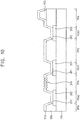
- FIGS. 7 , 8 , 9 , 10 , 11 , and 2 are cross-sectional views illustrating structures formed in a method of manufacturing an organic light emitting display device according to an embodiment.
- a method of manufacturing the OLED device described with reference to FIGS. 1 to 3 is described with reference to FIGS. 7 through 11 .
- the method of manufacturing the OLED device described with reference to FIGS. 7 through 11 may also apply to the OLED device described with reference to FIG. 4 and the OLED device described with reference to FIGS. 5 and 6 .
- a conductive material may be deposited on the substrate 100, and may be patterned to form the first to third pixel electrodes 201, 202, and 203.
- a photosensitive organic material may be deposited on the substrate 100 and on the first to third pixel electrodes 201, 202, and 203 to form a preliminary pixel defining layer 301.
- the preliminary pixel defining layer 301 may include a positive photosensitive organic material in which a portion exposed to light is removed.
- the preliminary pixel defining layer 301 may include a negative photosensitive organic material in which a portion exposed to light is hardened.
- a halftone mask 700 may be disposed over the preliminary pixel defining layer 301, and the preliminary pixel defining layer 301 may be exposed using the halftone mask 700.
- the halftone mask 700 may include a light transmitting portion 710 (or transparent portion 710), a light shielding portion 720, and a semi-light transmitting portion 730 (or translucent portion 730 or semitransparent portion 730).
- the light transmitting portion 710 may transmit light
- the light shielding portion 720 may block light
- the semi-light transmitting portion 730 may transmit a part of light.
- a light transmittance of the semi-light transmitting portion 730 may be less than a light transmittance of the light transmitting portion 710 and greater than a light transmittance of the light shielding portion 720.
- the pixel defining layer 300 may be formed on the substrate 100 and may partially expose the first to third pixel electrodes 201, 202, and 203.
- the preliminary pixel defining layer 301 irradiated with light through the halftone mask 700 may be developed to form the pixel defining layer 300.
- a portion of the preliminary pixel defining layer 301 corresponding to the light transmitting portion 710 may be substantially entirely removed, and a portion of the preliminary pixel defining layer 301 corresponding to the light shielding portion 720 may substantially remain.
- a portion of the preliminary pixel defining layer 301 corresponding to the semi-light transmitting portion 730 may be partially removed.
- the pixel defining layer 300 may include the first to third opening portions OP1, OP2, and OP3 corresponding to light transmitting portion 710 and respectively exposing the first to third pixel electrodes 201, 202, and 203, may include portions corresponding to the light shielding portion 720 and having a first thickness, and may include portions corresponding to the semi-light transmitting portion 730 and having a second thickness less than the first thickness. Portions in the pixel defining layer 300 having the first thickness may correspond to convex portions of the uneven structure 310 and the substantially flat (or planarized) upper surface, and portions in the pixel defining layer 300 having the second thickness may correspond to concave portions of the uneven structure 310.
- the pixel defining layer 300 may be formed using the halftone mask 700, so that the opening portions OP1, OP2, and OP3 and the upper surface at which the uneven structure 310 may be formed by single photolithography process. Therefore, manufacturing time and cost of the OLED device may be minimized.
- a photosensitive organic material may be deposited on the pixel defining layer 300, and may be patterned to form the spacer 400. Then, a hole injecting material may be deposited on the pixel defining layer 300 and on the spacer 400 to form the hole injection layer 510.
- the hole injection layer 510 may be formed using at least one of various methods such as vacuum deposition, spin coating, casting, Langmuir-Blodgett (LB) deposition, ink-jet printing, laser-printing, and laser-induced thermal imaging.
- the hole injection layer 510 may be formed along profiles of the first to third pixel electrodes 201, 202, and 203 and the pixel defining layer 300.
- the hole injection layer 510 may be formed along a profile of the uneven structure 310 formed at the upper surface of the pixel defining layer 300.
- a hole transporting material may be deposited on the hole injection layer 510 to form the hole transport layer 520.
- the hole transport layer 520 may be formed along a profile of the hole injection layer 510.
- the hole transport layer 520 may be formed along a profile of the uneven structure 310 formed at the upper surface of the pixel defining layer 300.
- an organic light emitting material may be injected on the hole transport layer 520 to form the first to third emission layers 531, 532, and 533.
- the hole transport layer 520 and the first to third emission layers 531, 532, and 533 may be formed using at least one of various methods such as vacuum deposition, spin coating, casting, Langmuir-Blodgett (LB) deposition, ink-jet printing, laser-printing, and laser-induced thermal imaging.
- various methods such as vacuum deposition, spin coating, casting, Langmuir-Blodgett (LB) deposition, ink-jet printing, laser-printing, and laser-induced thermal imaging.
- an electron transporting material may be deposited on the hole transport layer 520 and on the first to third emission layers 531, 532, and 533 to form the electron transport layer 540.
- the electron transport layer 540 may be formed using at least one of various methods such as vacuum deposition, spin coating, casting, Langmuir-Blodgett (LB) deposition, ink-jet printing, laser-printing, and laser-induced thermal imaging.
- LB Langmuir-Blodgett
- an electron injecting material may be deposited on the electron transport layer 540 to form the electron injection layer.
- a conductive material may be deposited on the electron transport layer 540 to form the common electrode 600.
- the electron transport layer 540 and the common electrode 600 may be formed along profiles of the first to third emission layers 531, 532, and 533 and the hole transport layer 520.
- the electron transport layer 540 and the common electrode 600 may be formed along a profile of the uneven structure 310 formed at the upper surface of the pixel defining layer 300.
- embodiments can provide an organic light emitting display, OLED, device, comprising: a substrate; a first pixel electrode, and a second pixel electrode, each overlapping the substrate; a pixel defining layer comprising a first opening and a second opening respectively partially exposing the first pixel electrode and the second pixel electrode, wherein the pixel defining layer further comprises a first uneven surface and a first flat face, wherein the first uneven surface is opposite the first flat face and is positioned between the first opening and the second opening, and wherein the first flat face is positioned between the first pixel electrode and the second pixel electrode and is positioned between the first uneven surface and the substrate; a first emission layer, and a second emission layer respectively corresponding to the first opening, and the second opening; and a common electrode overlapping each of the first emission layer and the second emission layer.
- the first uneven surface may be a surface of the pixel defining layer that faces away from the substrate, and the first flat face may be a surface of the pixel defining layer that faces the substrate.
- the surface of the pixel defining layer that faces away from the substrate may have portions that are uneven (e.g. forming an uneven surface such as the first uneven surface) and portions that are flat (e.g. regions between two uneven surface regions).
- the first uneven surface may be a surface that comprises a series of protrusions and cavities (or depressions). Layers over the first uneven surface may conform to the shape of the first uneven surface in the region of the first uneven surface (i.e. at overlapping portions).
- the uneven structure may include a plurality of concave portions (or cavities/depressions) and a plurality of convex portions (or protrusions).
- the concave portions may be recessed from the upper surface of the pixel defining layer toward the substrate, and the convex portions may protrude toward the common electrode.
- the concave portions and the convex portions may be alternatively arranged.
- the pixel defining layer may be disposed over the substrate and between the first pixel electrode and the second pixel electrode, with the first opening and the second opening respectively partially exposing the first pixel electrode and the second pixel electrode.
- a hole injection layer may be provided that directly contacts each of the first pixel electrode, the second pixel electrode, and the pixel defining layer.
- the hole injection layer may directly contact surfaces of the first pixel electrode and the second pixel electrode that face away from the substrate and the first uneven surface.
- the hole injection layer may conform to the shape of the first uneven surface.
- the resistance of the hole injection layer in the region of the first uneven surface may therefore be increased.
- Layers over the hole injection layer may conform to the shape of the first uneven surface in the region of the first uneven surface (i.e. at overlapping portions).
- the OLED device may further comprise a third pixel electrode overlapping the substrate, wherein the pixel defining layer comprises a third opening partially exposing the third pixel electrode; and a third emission layer corresponding to the third opening; wherein the common electrode overlaps each of the first emission layer and the second emission layer, and the third emission layer.
- the first pixel electrode, a second pixel electrode, and a third pixel electrode may respectively correspond to pixels of a pixel unit, for example respectively emitting red light, green light, and blue light.
- the OLED device may comprise a plurality of pixels forming pixel units.
- Embodiments can provide a method of manufacturing an OLED device, the method comprising: forming a first pixel electrode, a second pixel electrode, and a third pixel electrode over a substrate; forming a pixel defining layer over the substrate, wherein the pixel defining layer comprises a first opening, a second opening, and a third opening respectively partially exposing the first pixel electrode, the second pixel electrode, and the third pixel electrode, wherein the pixel defining layer further comprises an uneven surface and a first flat face, wherein the uneven surface is opposite the first flat face and is positioned between the first opening and the second opening, and wherein the first flat face is positioned between the first pixel electrode and the second pixel electrode and is positioned between the uneven surface and the substrate; forming a first emission layer, a second emission layer, and a third emission layer that respectively correspond to the first opening, the second opening, and the third opening; and forming a common electrode that overlaps each of the first emission layer, the second emission layer, and the third emission layer.
- An organic light emitting display device may be applied to a display device included in a computer, a notebook, a mobile phone, a smartphone, a smart pad, a PMP, a PDA, an MP3 player, or the like.
Landscapes
- Physics & Mathematics (AREA)
- Optics & Photonics (AREA)
- Engineering & Computer Science (AREA)
- Microelectronics & Electronic Packaging (AREA)
- Manufacturing & Machinery (AREA)
- Electroluminescent Light Sources (AREA)
Abstract
Description
- The technical field relates to an organic light emitting display device and a method of manufacturing an organic light emitting display device.
- Organic light emitting display (OLED) devices are self-luminous display devices that use organic light emitting diodes to emit light to display images. An OLED device does not require a separate light source; thus, the thickness and weight of the OLED device can be minimized.
- An OLED device may include a plurality of pixels. If electric charges undesirably flow from one pixel (of a certain color) into another pixel (of another color) during operation of the OLED device, the quality of images displayed by the OLED device may be unsatisfactory.
- Embodiments may be related to an organic light emitting display (OLED) device in which lateral leakage current between pixels may be minimized.
- Embodiments may be related to a method of manufacturing the OLED device.
- An OLED device according to embodiments may include the following elements: a substrate including a first pixel area, a second pixel area, a third pixel area, and a peripheral area surrounding the first to third pixel areas; a first pixel electrode, a second pixel electrode, and a third pixel electrode disposed on the substrate, the first pixel electrode, the second pixel electrode, and the third pixel electrode respectively overlapping the first pixel area, the second pixel area, and the third pixel area; a pixel defining layer disposed on the substrate, the pixel defining layer overlapping the peripheral area and having an upper surface at which an uneven structure is formed between the first pixel area and the second pixel area; a hole injection layer disposed on the first to third pixel electrodes and the pixel defining layer, the hole injection layer being formed along a profile of the upper surface of the pixel defining layer; a first emission layer, a second emission layer, and a third emission layer disposed on the hole injection layer, the first emission layer, the second emission layer, and the third emission layer respectively overlapping the first pixel area, the second pixel area, and the third pixel area; and a common electrode disposed on the first to third emission layers and the hole injection layer.
- In an embodiment, the uneven structure may be formed only between the first pixel area and the second pixel area.
- In an embodiment, the upper surface of the pixel defining layer between the first pixel area and the third pixel area may be flat.
- In an embodiment, a distance between the first pixel area and the second pixel area may be less than a distance between the first pixel area and the third pixel area.
- In an embodiment, the uneven structure may be further formed at the upper surface of the pixel defining layer between the first pixel area and the third pixel area.
- In an embodiment, a portion of the upper surface of the pixel defining layer at which the uneven structure is not formed may be flat.
- In an embodiment, the second pixel area may be located in a first direction from the first pixel area, and the uneven structure may include concave portions and convex portions alternatively arranged along the first direction.
- In an embodiment, each of the concave portions may extend in a second direction perpendicular to the first direction and parallel to the substrate.
- In an embodiment, lengths of the concave portions may be uniform.
- In an embodiment, lengths of the concave portions may increase as being away from the first pixel area or the second pixel area.
- In an embodiment, the OLED device may further include a spacer disposed between the pixel defining layer and the hole injection layer, the spacer overlapping the peripheral area and not overlapping the uneven structure.
- In an embodiment, the first emission layer, the second emission layer, and the third emission layer may respectively emit a red light, a green light, and a blue light.
- In an embodiment, the OLED device may further include a hole transport layer disposed between the hole injection layer and the first to third emission layers, the hole transport layer being formed along a profile of the upper surface of the pixel defining layer.
- In an embodiment, the OLED device may further include an electron transport layer disposed between the first to third emission layers and the common electrode, the electron transport layer being formed along a profile of the upper surface of the pixel defining layer.
- An OLED device according to embodiments may include the following elements: a plurality of pixels each including a pixel electrode, a hole injection layer, an emission layer, and a common electrode which are sequentially stacked; and a pixel defining layer dividing the plurality of pixels, the pixel defining layer having an upper surface at which an uneven structure is formed between the plurality of pixels. The hole injection layer may be formed commonly over the plurality of pixels and along a profile of the upper surface of the pixel defining layer.
- In an embodiment, a portion of the upper surface of the pixel defining layer at which the uneven structure is not formed may be flat.
- In an embodiment, the uneven structure may include concave portions and convex portions alternatively arranged between the plurality of pixels.
- A method of manufacturing an OLED device according to embodiments may include the following steps: forming a first pixel electrode, a second pixel electrode, and a third pixel electrode on the substrate, the first pixel electrode, the second pixel electrode, and the third pixel electrode respectively overlapping the first pixel area, the second pixel area, and the third pixel area; forming a pixel defining layer on the substrate, the pixel defining layer overlapping a peripheral area surrounding the first to third pixel areas and having an upper surface at which an uneven structure is formed between the first pixel area and the second pixel area; forming a hole injection layer on the first to third pixel electrodes and the pixel defining layer, the hole injection layer being formed along a profile of the upper surface of the pixel defining layer; forming a first emission layer, a second emission layer, and a third emission layer on the hole injection layer, the first emission layer, the second emission layer, and the third emission layer respectively overlapping the first pixel area, the second pixel area, and the third pixel area; and forming a common electrode on the first to third emission layers and the hole injection layer.
- In an embodiment, the second pixel area may be located in a first direction from the first pixel area, and the uneven structure may include concave portions and convex portions alternatively arranged along the first direction.
- In an embodiment, forming the pixel defining layer may include forming a preliminary pixel defining layer on the substrate on which the first to third pixel electrodes are formed, providing a halftone mask over the preliminary pixel defining layer, and exposing and developing the preliminary pixel defining layer using the halftone mask.
- In an embodiment, the halftone mask may include light transmitting portions, light shielding portions, and semi-light transmitting portions. The light transmitting portions may correspond to opening portions of the pixel defining layer respectively exposing the first to third pixel electrodes, the light shielding portions may correspond to the convex portions of the uneven structure, and the semi-light transmitting portions may correspond to the concave portions of the uneven structure.
- An embodiment may be related to an organic light emitting display (OLED) device. The OLED device may include the following elements: a substrate; a first pixel electrode, a second pixel electrode, and a third pixel electrode each overlapping the substrate; a pixel defining layer including a first opening, a second opening, and a third opening respectively partially exposing the first pixel electrode, the second pixel electrode, and the third pixel electrode, wherein the pixel defining layer may include a first uneven surface and a first flat face, wherein the first uneven surface may be opposite the first flat face and may be positioned between the first opening and the second opening, and wherein the first flat face may be positioned between the first pixel electrode and the second pixel electrode and may be positioned between the first uneven surface and the substrate; a first emission layer, a second emission layer, and a third emission layer respectively corresponding to the first opening, the second opening, and the third opening; and a common electrode overlapping each of the first emission layer, the second emission layer, and the third emission layer.
- The first uneven surface may be only positioned between the first emission layer and the second emission layer.
- The first uneven surface may be positioned between two opposite parallel faces of the first emission layer.
- A surface of the pixel defining layer may be positioned not farther from the common electrode than any other surfaces of the pixel defining layer, may be positioned between the first opening and the third opening, and may be flat.
- A minimum distance between the first emission layer and the second emission layer may be less than a minimum distance between the first emission layer and the third emission layer.
- The pixel defining layer may include a second uneven surface and a second flat face. The second uneven surface may be positioned between the first opening and the third opening and may be opposite the second flat face. The second flat face may be positioned between the first pixel electrode and the third pixel electrode and may be positioned between the second uneven surface and the substrate.
- A surface of the pixel defining layer may be positioned not farther from the common electrode than any other surfaces of the pixel defining layer, may be positioned between the second opening and the third opening, and may be flat.
- The first uneven surface may include cavities and protrusions alternatively arranged between the first opening and the second opening.
- A lengthwise direction of each of the cavities may be parallel to an edge of the first opening and may be parallel to the substrate.
- Lengths of the cavities may be equal.
- The cavities include a first cavity and a second cavity. The first cavity may be positioned closer to the first opening than the second cavity and may be shorter than the second cavity.
- The OLED device may include the following elements: a hole injection layer directly contacting each of the first pixel electrode, the second pixel electrode, the third pixel electrode, and the pixel defining layer; and a spacer disposed between the pixel defining layer and the hole injection layer and directly contacting a second flat face of the pixel defining layer. The hole injection layer may include cavities. The cavities may be positioned between the first opening and the second opening. The second flat face of the pixel defining layer may extend from an edge of the second opening to an edge of the third opening and may be spaced from the first uneven surface.
- The first emission layer, the second emission layer, and the third emission layer may be respectively configured to emit a red light, a green light, and a blue light. The first emission layer and the second emission layer may immediately neighbor each other with no intervening emission layer between the first emission layer and the second emission layer.
- The OLED device may include the following elements: a hole injection layer directly contacting each of the first pixel electrode, the second pixel electrode, the third pixel electrode, and the pixel defining layer; and a hole transport layer disposed between the hole injection layer and each of the first emission layer, the second emission layer, and the third emission layer. The hole transport layer may overlap the pixel defining layer and may include cavities. The cavities may be positioned between the first opening and the second opening.
- The OLED device may include an electron transport layer disposed between the common electrode and each of the first emission layer, the second emission layer, and the third emission layer, the electron transport layer overlapping the pixel defining layer.
- An embodiment may be related to an OLED device. The OLED device may include the following elements: a common electrode; a first pixel electrode overlapping the common electrode; a first emission layer positioned between the first pixel electrode and the common electrode; a second pixel electrode; a second emission layer positioned between the second pixel electrode and the common electrode; and a pixel defining layer including a first opening, a second opening, a first flat face, and an uneven surface structure, wherein the first opening partially exposes the first pixel electrode, wherein the second opening partially exposes the second pixel electrode, wherein the first flat face may be opposite the uneven surface, may be positioned between the first pixel electrode and the second pixel electrode, and may extend from the first pixel electrode to the second pixel electrode, and wherein the uneven surface may be positioned between the fist opening and the second opening.
- The OLED device may include the following elements: a third pixel electrode; and a third emission layer positioned between the third pixel electrode and the common electrode. The pixel defining layer may include a third opening, a second flat face, and a third flat face. The third opening may partially expose the third pixel electrode. The second flat face may be opposite the third flat face, may be positioned between the second pixel electrode and the third pixel electrode, and may extend from the second pixel electrode to the third pixel electrode. The third flat face may be positioned between the second opening and the third opening and may extend from the second opening to the third opening.
- The uneven surface may include cavities and protrusions alternatively arranged between the first opening and the second opening.
- An embodiment may be related to a method of manufacturing an OLED device. The method may include the following steps: forming a first pixel electrode, a second pixel electrode, and a third pixel electrode on a substrate; forming a pixel defining layer on the substrate, wherein the pixel defining layer may include a first opening, a second opening, and a third opening respectively partially exposing the first pixel electrode, the second pixel electrode, and the third pixel electrode, wherein the pixel defining layer may include an uneven surface and a first flat face, wherein the uneven surface may be opposite the first flat face and may be positioned between the first opening and the second opening, and wherein the first flat face may be positioned between the first pixel electrode and the second pixel electrode and may be positioned between the uneven surface and the substrate; forming a first emission layer, a second emission layer, and a third emission layer that respectively correspond to the first opening, the second opening, and the third opening; and forming a common electrode that overlaps each of the first emission layer, the second emission layer, and the third emission layer.
- The uneven surface may include cavities and protrusions alternatively arranged between the first opening and the second opening.
- Forming the pixel defining layer may include the following steps: forming a material layer on the substrate, the first pixel electrode, the second pixel electrode, and the third pixel electrode; providing a halftone mask over the material layer; and exposing and developing the material layer using the halftone mask.
- The halftone mask may include light transmitting portions, light shielding portions, and semi-light transmitting portions. The light transmitting portions may correspond to the first opening, the second opening, and the third opening. The light shielding portions may correspond to the protrusions of the uneven surface structure. The semi-light transmitting portions may correspond to the cavities of the uneven surface structure.
- An OLED device according to an embodiment may include a pixel defining layer having an upper surface with an uneven structure between pixels, and a hole injection layer may be formed on the pixel defining layer. Accordingly, an electrical path of the hole injection layer between the pixels may lengthen, and lateral leakage current between the pixels through the hole injection layer may decrease.
- In a method of manufacturing the OLED device according to some embodiments, the pixel defining layer may be formed using a halftone mask so that the pixel defining layer having opening portions and an uneven upper surface may be formed by single photolithography process. Therefore, manufacturing time and/or cost of the OLED device may be minimized.
- According to an aspect, there is provided an OLED device as set out in claim 1. Additional features are set out in claims 2 to 13. According to an aspect, there is provided a method as set out in claim 14. Additional features are set out in claim 15.
-
-
FIG. 1 is a plan view illustrating an organic light emitting display (OLED) device according to an embodiment. -
FIG. 2 is a cross-sectional view taken along a line II-II' inFIG. 1 according to an embodiment. -
FIG. 3 is a cross-sectional view illustrating a pixel defining layer and a hole injection layer inFIG. 2 according to an embodiment. -
FIG. 4 is a plan view illustrating an OLED device according to an embodiment. -
FIG. 5 is a plan view illustrating an OLED device according to an embodiment. -
FIG. 6 is a cross-sectional view taken along a line VI-VI' inFIG. 5 according to an embodiment. -
FIGS. 7 ,8 ,9 ,10 , and11 are cross-sectional views illustrating structures formed in a method of manufacturing an OLED device according to an embodiment. - Example embodiments are explained with reference to the accompanying drawings.
- Although the terms "first," "second," etc. may be used to describe various elements, these elements, should not be limited by these terms. These terms may be used to distinguish one element from another element. A first element may be termed a second element without departing from teachings of one or more embodiments. The description of an element as a "first" element may not require or imply the presence of a second element or other elements. The terms "first," "second," etc. may be used to differentiate different categories or sets of elements. For conciseness, the terms "first," "second," etc. may represent "first-type (or first-set)," "second-type (or second-set)," etc., respectively.
-
FIG. 1 is a plan view illustrating an OLED according to an embodiment.FIG. 2 is a cross-sectional view taken along a line II-II' inFIG. 1 according to an embodiment.FIG. 3 is a cross-sectional view illustrating a pixel defining layer and a hole injection layer inFIG. 2 according to an embodiment. - Referring to
FIGS. 1 ,2 , and3 , the OLED device may include asubstrate 100, a plurality ofpixel electrodes pixel defining layer 300; aspacer 400, ahole injection layer 510, ahole transport layer 520, a plurality ofemission layers electron transport layer 540, and acommon electrode 600. The OLED device may include a plurality of pixels PX1, PX2, and PX3 defined by the plurality ofpixel electrodes hole injection layer 510, thehole transport layer 520, the plurality ofemission layers electron transport layer 540, and thecommon electrode 600. Boundaries of the pixels and/or boundaries of pixel areas associated with the pixels may correspond to edges of openings of thepixel defining layer 300. - The
substrate 100 may be substantially formed of transparent glass containing SiOx. Thesubstrate 100 may be formed of a plastic material. Although not shown in the figures, thesubstrate 100 may include at least one thin film transistor and/or a capacitor for driving each pixel; a circuit for driving the pixel may use the thin film transistor, the capacitor, and the like. - The
substrate 100 may include a plurality of pixel areas PXA1, PXA2, and PXA3 and a peripheral area PPA. The pixel areas PXA1, PXA2, and PXA3 may include a plurality of first pixel areas PXA1, a plurality of second pixel areas PXA2, and a plurality of third pixel areas PXA3. A first pixel area PXA1, a second pixel area PXA2, and a third pixel area PXA3 may be spaced apart from each other. For example, when the first pixel area PXA1 is spaced from the second pixel area PXA2 in a first direction DR1, the third pixel area PXA3 may be spaced from the second pixel area PXA2 in a second direction DR2 perpendicular to the first direction DR1. For example, when the first pixel area PXA1 is spaced from the second pixel area PXA2 in the second direction DR2, the third pixel area PXA3 may be spaced from the second pixel area PXA2 in the first direction DR1. Further, the third pixel area PXA3 may be spaced from the first pixel area PXA1 in a third direction DR3 or in a fourth direction DR4 perpendicular to the third direction DR3. For example, the third direction DR3 may be inclined by about 45 degrees in a clockwise direction from the first direction DR1, and the fourth direction DR4 may be inclined by about 45 degrees in a clockwise direction from the second direction DR2. Boundaries of the pixel areas PXA1, PXA2, and PXA3 may respectively correspond to (bottom) boundaries of openings OP1, OP2, and OP3 of thepixel defining layer 300. - In an embodiment, a distance between the first pixel area PXA1 and the second pixel area PXA2 is less than a distance between the first pixel area PXA1 and the third pixel area PXA3. For example, a distance D12 between the first pixel area PXA1 and the second pixel area PXA2 may be about 19.2 µm, and a distance D13 between the first pixel area PXA1 and the third pixel area PXA3 may be about 25.9 µm. The peripheral area PPA may surround the pixel areas PXA1, PXA2, and PXA3.
- The
pixel electrodes substrate 100. Thepixel electrodes first pixel electrode 201, asecond pixel electrode 202, and athird pixel electrode 203. Thefirst pixel electrode 201, thesecond pixel electrode 202, and thethird pixel electrode 203 may overlap the first pixel area PXA1, the second pixel area PXA2, and the third pixel area PXA3, respectively. The first tothird pixel electrodes - The
pixel defining layer 300 may be disposed on thesubstrate 100. Thepixel defining layer 300 may include a plurality of opening portions OP1, OP2, and OP3 (or openings OP1, OP2, and OP3). The opening portions OP1, OP2, and OP3 may include a first opening portion OP1, a second opening portion OP2, and a third opening portion OP3. The first opening portion OP1, the second opening portion OP2, and the third opening portion OP3 may expose thefirst pixel electrode 201, thesecond pixel electrode 202, and thethird pixel electrode 203, respectively. For example, the first to third opening portions OP1, OP2, and OP3 may respectively cover edge portions of the first tothird pixel electrodes third pixel electrodes pixel defining layer 300 may overlap the peripheral area PPA. The opening portions OP1, OP2, and OP3 may define the pixels PX1, PX2, and PX3, respectively. In other words, thepixel defining layer 300 may divide the pixels PX1, PX2, and PX3 from each other. Thepixel defining layer 300 may include a photosensitive organic insulation material. - The pixels PX1, PX2, and PX3 may include a first pixel PX1, a second pixel PX2, and a third pixel PX3 emitting different colors of light. In an embodiment, the first pixel PX1, the second pixel PX2, and the third pixel PX3 may be a red pixel emitting red light, a green pixel emitting green light, and a blue pixel emitting blue light, respectively. Each of the pixels PX1, PX2, and PX3 may include one of the
pixel electrode hole injection layer 510, a portion of thehole transport layer 520, one of theemission layer electron transport layer 540, and a portion of thecommon electrode 600. - An
uneven structure 310 may be formed at an upper surface of thepixel defining layer 300. Theuneven structure 310 may be formed between the pixels PX1, PX2, and PX3. In an embodiment, one or moreuneven structures 310 may be formed between the first pixel area PXA1 and other pixel areas PXA2 and PXA3. In other words, one or moreuneven structures 310 may be formed between the first pixel area PXA1 and the second pixel area PXA2 and/or between the first pixel area PXA1 and the third pixel area PXA3. In another embodiment, anuneven structure 310 may also be formed between the second pixel area PXA2 and the third pixel area PXA3. An upper surface of thepixel defining layer 300 at which nouneven structure 310 is formed may be substantially flat (or planarized). - In an embodiment, the
uneven structure 310 may be formed only between the first pixel area PXA1 and the second pixel area PXA2, and nouneven structure 310 may be formed between the first pixel area PXA1 and the third pixel area PXA3. In such an embodiment, an upper surface of thepixel defining layer 300 between the first pixel area PXA1 and the third pixel area PXA3 may be substantially flat (or planarized). - The
uneven structure 310 may include a plurality of concave portions 311 (or cavities 311) and a plurality of convex portions 312 (or protrusions 312). Theconcave portions 311 may be recessed from the upper surface of thepixel defining layer 300 toward thesubstrate 100, and theconvex portions 312 may protrude toward thecommon electrode 600. Theconcave portions 311 and theconvex portions 312 may be alternatively arranged along the first direction DR1 or the second direction DR2 in which the second pixel area PXA2 is spaced from the first pixel area PXA1. - The
uneven structure 310 may have a predetermined thickness TH. For example, the thickness TH of theuneven structure 310 may be about 1.4 µm. For example, the thickness TH of theuneven structure 310 may correspond to a depth of theconcave portion 311 of theuneven structure 310. Theuneven structure 310 may include uneven units periodically formed by theconcave portions 311 and theconvex portions 312 which are alternatively arranged, and the uneven unit may have a predetermined width WD. For example, the width WD of the uneven unit may be about 2.9 µm. For example, the width WD of the uneven unit may correspond to a sum of a width of theconcave portion 311 and a width of theconvex portion 312. Because theuneven structure 310 is formed at the upper surface of thepixel defining layer 300, an electrical path length of the upper surface of thepixel defining layer 300 which is defined along theconcave portions 311 and theconvex portions 312 of theuneven structure 310 may increase. - Each of the
concave portions 311 may extend along a direction perpendicular to a direction along which theconcave portions 311 and theconvex portions 312 are alternatively arranged and parallel to thesubstrate 100. For example, when theconcave portions 311 and theconvex portions 312 are alternatively arranged along the first direction DR1, each of theconcave portions 311 may extend in the second direction DR2 and may extend perpendicular to the nearest edges of the openings of thepixel defining layer 300; the lengthwise directions of theconcave portions 311 may be the second direction DR2. Further, when theconcave portions 311 and theconvex portions 312 are alternatively arranged along the second direction DR2, each of theconcave portions 311 may extend in the first direction DR1; the lengthwise directions of theconcave portions 311 may be the first direction DR1. - In an embodiment, lengths L1 of the
concave portions 311 may be substantially equal to one another. For example, the length L1 of theconcave portion 311 may be a length in a lengthwise direction of theconcave portion 311. Theconcave portions 311 may have substantially the same lengths L1. -
Spacers 400 may be disposed on thepixel defining layer 300. Aspacer 400 may overlap the peripheral area PPA. Thespacer 400 may not overlap theuneven structure 310. Nospacer 400 may be formed between the first pixel area PXA1 and other pixel areas PXA2 and PXA3. Thespacer 400 may support an encapsulation substrate, an encapsulation layer, etc. formed over the pixels PX1, PX2, and PX3, and may separate the encapsulation substrate, the encapsulation layer, etc. from the pixels PX1, PX2, and PX3 to protect the pixels PX1, PX2, and PX3. Thespacer 400 may include a photosensitive organic insulation material. In an embodiment, thespacer 400 may include substantially the same material as that of thepixel defining layer 300 and may be significantly wider than eachconcave portion 311, eachconvex portion 312, multipleconcave portions 311, and/or multipleconvex portions 312 in a width direction of eachconcave portion 311 or eachconvex portion 312. - The
hole injection layer 510 may be disposed on the first tothird pixel electrodes pixel defining layer 300, and thespacer 400. Thehole injection layer 510 may be commonly formed over the first to third pixels PX1, PX2, and PX3. Thehole injection layer 510 may be located over an entire upper surface of thesubstrate 100. - The
hole injection layer 510 may serve to improve the injection of holes from each of thepixel electrodes hole transport layer 520. Thehole injection layer 510 may include one or more phthalocyanine compounds such as at least one of copper phthalocyanine, polyaniline/dodecylbenzenesulfonic acid (PANI/DBSA), 4,4',4"-tris { N,-(2-naphthyl)-N-phenylamino }-triphenylamine (2TNATA), 4,4',4"-tris(3-methylphenylphenylamino)triphenylamine (m-MTDATA), 4,4'4"-Tris(N,N-diphenylamino)triphenylamine (TDATA), polyaniline/camphor sulfonic acid (PANI/CSA), polyaniline/poly(4-styrenesulfonate) (PANI/PSS), N,N-diphenyl-N,N-bis-[4-(phenyl-m-tolyl-amino)-phenyl]-biphenyl-4,4'-diamine (DNTPD), and poly(3,4-ethylenedioxythiophene)/poly(4-styrenesulfonate) (PEDOT/PS S). - The
hole injection layer 510 may be formed along profiles of the first tothird pixel electrodes pixel defining layer 300 on thesubstrate 100. Thehole injection layer 510 may be formed along a profile of the upper surface of thepixel defining layer 300. Thehole injection layer 510 may be formed along a profile of theuneven structure 310 formed at the upper surface of thepixel defining layer 300 between the first pixel area PXA1 and the second pixel area PXA2. Further, thehole injection layer 510 may be formed along a profile of the substantially flat (or planarized) upper surface of thepixel defining layer 300 between the first pixel area PXA1 and the third pixel area PXA3. - Since the
hole injection layer 510 is formed between the first pixel area PXA1 and the second pixel area PXA2 along a profile of the upper surface of thepixel defining layer 300 at which theuneven structure 310 is formed, a length of thehole injection layer 510 between the first pixel area PXA1 and the second pixel area PXA2 may increase. For example, when a horizontal distance D12 between the first pixel area PXA1 and the second pixel area PXA2 is about 19.2 µm, if an upper surface of thepixel defining layer 300 between the first pixel area PXA1 and the second pixel area PXA2 is substantially flat (or planarized) in a comparative example, a length of thehole injection layer 510 between the first pixel area PXA1 and the second pixel area PXA2 may be about 21.5 µm. In an embodiment, theuneven structure 310 is formed at the upper surface of thepixel defining layer 300 between the first pixel area PXA1 and the second pixel area PXA2, such that a length of thehole injection layer 510 between the first pixel area PXA1 and the second pixel area PXA2 may be about 28.0 µm. Therefore, when theuneven structure 310 is formed at the upper surface of thepixel defining layer 300, the length of thehole injection layer 510 may increase by about 1.3 times. - The
hole injection layer 510 may be formed of a material having a relatively high charge mobility. When formed as a common layer over the pixels PX1, PX2, and PX3, thehole injection layer 510 may become a path for the movement of electric charges (holes) between the pixels PX1, PX2, and PX3. Accordingly, when one pixel is driven, lateral leakage current may flow through an adjacent pixel via thehole injection layer 510 if thehole injection layer 510 provides a sufficiently short electrical path. Thehole injection layer 510 may function as a conductive medium between the adjacent pixels PX1, PX2, and PX3, and an electrical resistance R of thehole injection layer 510 that functions as the conductive medium is illustrated in a mathematical equation below.
- The p represents a resistivity of the
hole injection layer 510, the L represents an electrical path length of thehole injection layer 510, the W represents an electrical path width of thehole injection layer 510, and the t represents an electrical path thickness of thehole injection layer 510. - The first pixel PX1 emitting red light may have a relatively low turn-on voltage. When an electrical path between the first pixel area PXA1 and the second pixel area PXA2 is relatively short, according to driving of the second pixel PX2, the first pixel PX1 may emit light in response to lateral leakage current transmitted from the second pixel PX2 to the first pixel PX1 via the
hole injection layer 510, and color-mixing may occur at low luminance. According to an embodiment, thehole injection layer 510 may be formed along the upper surface of thepixel defining layer 300 at which theuneven structure 310 is formed between the first pixel area PXA1 and the second pixel area PXA2, so that the electrical path length L of thehole injection layer 510 between the first pixel area PXA1 and the second pixel area PXA2 may increase; therefore, the electrical resistance R of thehole injection layer 510 between the first pixel area PXA1 and the second pixel area PXA2 may increase. Accordingly, the magnitude of the lateral leakage current between the first pixel PX1 and the second pixel PX2 via thehole injection layer 510 may decrease, and color-mixing at low luminance due to the lateral leakage current may be prevented. - The
hole transport layer 520 may be disposed on thehole injection layer 510. Thehole transport layer 520 may be commonly formed over the first to third pixels PX1, PX2, and PX3. Thehole transport layer 520 may be located over an entire upper surface of thesubstrate 100. - The
hole transport layer 520 may serve to smoothly transport holes transmitted from thehole injection layer 510. Thehole transport layer 520 may include one or more carbazole-based derivatives such as at least one of N-phenylcarbazole, polyvinylcarbazole, etc., fluorine-based derivatives, triphenylamine-based derivatives such as N,N'-bis(3-methylphenyl)-N,N'-diphenyl-[1,1-biphenyl]-4,4'-diamine (TPD), 4,4',4"-tris(N-carbazolyl)triphenylamine (TCTA), etc., N,N'-di(1-naphthyl)-N,N'-diphenylbenzidine (NPB), and 4,4'-cyclohexylidenebis[N,N-bis(4-methylphenyl)benzenamine] (TAPC). Thehole injection layer 510 may include the same material as that included in thehole transport layer 520 and may be doped with a P-type dopant for improving a hole injection characteristic by decreasing a driving voltage of each pixel. - The
hole transport layer 520 may be formed along a profile of thehole injection layer 510 disposed on thepixel defining layer 300. Thehole transport layer 520 may be formed along a profile of the upper surface of thepixel defining layer 300. Thehole transport layer 520 may be formed along a profile of theuneven structure 310 formed at the upper surface of thepixel defining layer 300 between the first pixel area PXA1 and the second pixel area PXA2. Further, thehole transport layer 520 may be formed along a profile of the substantially flat (or planarized) upper surface of thepixel defining layer 300 between the first pixel area PXA1 and the third pixel area PXA3. Since thehole transport layer 520 is formed between the first pixel area PXA1 and the second pixel area PXA2 along a profile of the upper surface of thepixel defining layer 300 at which theuneven structure 310 is formed, a length of thehole transport layer 520 between the first pixel area PXA1 and the second pixel area PXA2 may increase. - The emission layers 531, 532, and 533 may be formed on the
hole transport layer 520. The emission layers 531, 532, and 533 may include afirst emission layer 531, asecond emission layer 532, and athird emission layer 533. Thefirst emission layer 531, thesecond emission layer 532, and thethird emission layer 533 may overlap the first pixel area PXA1, the second pixel area PXA2, and the third pixel area PXA3, respectively. The first to third emission layers 531, 532, and 533 may include a host and a dopant. The first to third emission layers 531, 532, and 533 may include materials respectively emitting red color, green color, and blue color, and may be formed of a phosphorescent material or a fluorescent material. - The
first emission layer 531 emitting red light may include a host material that includes CBP (carbazole biphenyl) or mCP (1,3-bis(carbazol-9-yl), and may be formed of a phosphorescent material including a dopant including at least one selected from PIQIr(acac) (bis(1-phenylisoquinoline)acetylacetonate iridium), PQIr(acac) (bis(1-phenylquinoline)acetylacetonate iridium), PQIr(tris(1-phenylquinoline)iridium), and PtOEP (octaethylporphyrin platinum), or may be formed of a fluorescent material including PBD:Eu(DBM)3(Phen) or perylene. - The
second emission layer 532 emitting green light may include a host material that includes CBP or mCP, and may be formed of a phosphorescent material that includes a dopant material including Ir(ppy)3(fac-tris(2-phenylpyridine)iridium), or may be formed of a fluorescent material including Alq3(tris(8-hydroxyquinolino)aluminum). - The
third emission layer 533 emitting blue light may include a host material including CBP or mCP, and may be formed of a phosphorescent material that includes a dopant material including (4,6-F2ppy)2Irpic, or may be formed of a fluorescent material including at least one selected from a group of spiro-DPVBi, spiro-6P, distyryl benzene (DSB), distyrylarylene (DSA), a PFO-based polymer, and a PPV-based polymer. - The
electron transport layer 540 may be disposed on the first to third emission layers 531, 532, and 533 and thehole transport layer 520. Theelectron transport layer 540 may be commonly formed over the first to third pixels PX1, PX2, and PX3. Theelectron transport layer 540 may be located over an entire upper surface of thesubstrate 100. - The
electron transport layer 540 may transfer electrons from thecommon electrode 600 to the first to third emission layers 531, 532, and 533. Further, theelectron transport layer 540 may prevent or reduce instances of holes injected from the first tothird pixel electrodes common electrode 600 via the first to third emission layers 531, 532, and 533. That is, theelectron transport layer 540 may serve as a hole blocking layer, and may help combination of the holes and electrons in the first to third emission layers 531, 532, and 533. - The
electron transport layer 540 may include, e.g., at least one of tris (8-hydroxyquinolinato) aluminum (Alq3), 1,3,5-Tri(1-phenyl-1H-benzo[d]imidazol-2-yl)phenyl (TPBi), 2,9-dimethyl-4,7-diphenyl-1,10-phenanthroline (BCP), 4,7-diphenyl-1,10-phenanthroline (Bphen), 3-(4-Biphenylyl)-4-phenyl-5-tert-butylphenyl-1,2,4-triazole (TAZ), 4-(Naphthalen-1-yl)-3,5-diphenyl-4H-1,2,4-triazole(NTAZ), 2-(4-Biphenylyl)-5-(4-tert-butylphenyl)-1,3,4-oxadiazole (tBu-PBD). Bis(2-methyl-8-quinolinolato-N1,O8)-(1,1'-Biphenyl-4-olato)aluminum (BAlq), beryllium bis(benzoquinolin-10-olate) (Bebq2), 9,10-di(naphthalene-2-yl)anthracene (ADN), and a mixture. - The OLED device may further include an electron injection layer (not shown) disposed on the
electron transport layer 540. The electron injection layer may serve to improve the injection of electrons fromcommon electrode 600 to theelectron transport layer 540. When the OLED device includes theelectron transport layer 540 and the electron injection layer, theelectron transport layer 540 may be formed of a lanthanide metal such as at least one of LiF, LiQ, Li2O, BaO, NaCl, CsF, and Yb, or a halogenated metal such as RbCl and/or RbI. Further, the electron injection layer may be formed of a material in which an electron transfer material is mixed with an insulating organic metal salt. The organic metal salt may have an energy band gap of about 4 eV or more. For example, the organic metal salt may include a metal acetate, a metal benzoate, a metal acetoacetate, a metal acetylacetonate, or a metal stearate. - The
electron transport layer 540 may be formed along profiles of the first to third emission layers 531, 532, and 533 and thehole transport layer 520 disposed on thepixel defining layer 300. Theelectron transport layer 540 may be formed along a profile of the upper surface of thepixel defining layer 300. Theelectron transport layer 540 may be formed along a profile of theuneven structure 310 formed at the upper surface of thepixel defining layer 300 between the first pixel area PXA1 and the second pixel area PXA2. Further, theelectron transport layer 540 may be formed along a profile of the substantially flat (or planarized) upper surface of thepixel defining layer 300 between the first pixel area PXA1 and the third pixel area PXA3. Since theelectron transport layer 540 is formed between the first pixel area PXA1 and the second pixel area PXA2 along a profile of the upper surface of thepixel defining layer 300 at which theuneven structure 310 is formed, a length of theelectron transport layer 540 between the first pixel area PXA1 and the second pixel area PXA2 may increase. - The
common electrode 600 may be disposed on theelectron transport layer 540. Thecommon electrode 600 may be commonly formed over the first to third pixels PX1, PX2, and PX3. Thecommon electrode 600 may be located over an entire upper surface of thesubstrate 100. Thecommon electrode 600 may include at least one of a reflective conductive material, a transparent conductive material, and a semi-transparent conductive material. - When the OLED device is a bottom emission type in which an image may be displayed toward the
substrate 100, each of the first tothird pixel electrodes common electrode 600 may be a reflective electrode. The first tothird pixel electrodes common electrode 600 may be formed of a metal having a low work function such as at least one of Ag, Mg, Al, Pt, Au, Ni, Nd, Ir, Cr, Li, and Ca. - When the OLED device is a top emission type in which an image may be displayed toward the
common electrode 600, each of the first tothird pixel electrodes common electrode 600 may be a transparent electrode. The first tothird pixel electrodes common electrode 600 may be a thin film including a metal having a low work function such as at least one of Ag, Mg, Al, Pt, Au, Ni, Nd, Ir, Cr, Li, Ca, and a mixture. -
FIG. 4 is a plan view illustrating an organic light emitting display device according to an embodiment. - The OLED device described with reference to the
FIG. 4 may be substantially the same as or similar to the OLED device described with reference toFIGS. 1 to 3 except shapes and dimensions of the uneven structure. Accordingly, descriptions on above-described elements may not be repeated. - Referring to
FIG. 4 , lengths L2 of theconcave portions 311 of theuneven structure 310 formed at the upper surface of thepixel defining layer 300 may increase as being away from the first pixel area PXA1 or the second pixel area PXA2. For example, a length L2 of aconcave portion 311 may be a length in a lengthwise direction of theconcave portion 311. For example, the lengths L2 of theconcave portions 311 may sequentially increase along the first direction DR1 or the second direction DR2 from the first pixel area PXA1 to the midpoint between the first pixel area PXA1 and the second pixel area PXA2, and may sequentially decrease along the first direction DR1 or the second direction DR2 from the midpoint to the second pixel area PXA2. The lengths L2 of theconcave portions 311 may decrease as approaching the first pixel area PXA1 or the second pixel area PXA2, and may increase as being away from the first pixel area PXA1 or the second pixel area PXA2. - When the
uneven structure 310 is formed between the first pixel area PXA1 and the second pixel area PXA2, a leakage current path bypassing theuneven structure 310 may be formed between the first pixel area PXA1 and the second area PXA2. However, when the lengths of theconcave portions 311 increase as being away from the first pixel area PXA1 or the second pixel area PXA2, an electrical length of the leakage current path bypassing theuneven structure 310 may increase, therefore, the magnitude of the lateral leakage current between the first pixel PX1 and the second pixel PX2 may decrease or the generation of the lateral leakage current may be substantially prevented. -
FIG. 5 is a plan view illustrating an organic light emitting display device according to an embodiment.FIG. 6 is a cross-sectional view taken along a line VI-VI' inFIG. 5 according to an embodiment. - The OLED device described with reference to the
FIGS. 5 and6 may be substantially the same as or similar to the OLED device described with reference toFIGS. 1 to 3 except locations in which uneven structures are formed. Accordingly, descriptions on above-described elements may not be repeated. - Referring to
FIGS. 5 and6 , theuneven structures pixel defining layer 300 may be formed between the first pixel area PXA1 and the third pixel area PXA3 in addition to between the first pixel area PXA1 and the second pixel area PXA2. Theuneven structures uneven structure 310 formed between the first pixel area PXA1 and the second pixel area PXA2 and may include a seconduneven structure 320 formed between the first pixel area PXA1 and the third pixel area PXA3. An upper surface of thepixel defining layer 300 at which nouneven structures - The second
uneven structure 320 may include a plurality ofconcave portions 321 and a plurality ofconvex portions 322. Theconcave portions 321 and theconvex portions 322 may be alternatively arranged along the third direction DR3 or the fourth direction DR4 in which the third pixel area PXA3 is spaced from the first pixel area PXA1. - The
concave portions 321 may extend along a direction perpendicular to a direction along which theconcave portions 321 and theconvex portions 322 are alternatively arranged, perpendicular to nearest edges of openings of thepixel defining layer 300, and parallel to thesubstrate 100. For example, when theconcave portions 321 and theconvex portions 322 are alternatively arranged along the third direction DR3, each of theconcave portions 321 may extend in the fourth direction DR4. Further, when theconcave portions 321 and theconvex portions 322 are alternatively arranged along the fourth direction DR4, each of theconcave portions 321 may extend in the third direction DR3. - In an embodiment, lengths L3 of the
concave portions 321 may be substantially equal. For example, a length L3 of aconcave portion 321 may be a length in a length direction of theconcave portion 321. Theconcave portions 321 may have substantially the same lengths L3. - In another embodiment, lengths L3 of the
concave portions 321 may increase as being away from the first pixel area PXA1 or the third pixel area PXA3. For example, the lengths L3 of theconcave portions 321 may sequentially increase along the third direction DR3 or the fourth direction DR4 from the first pixel area PXA1 to the middle between the first pixel area PXA1 and the third pixel area PXA3, and may sequentially decrease along the third direction DR3 or the fourth direction DR4 from the middle to the third pixel area PXA3. The lengths L3 of theconcave portions 321 may decrease as approaching the first pixel area PXA1 or the third pixel area PXA3, and may increase as being away from the first pixel area PXA1 or the third pixel area PXA3. - The
hole injection layer 510 may be formed along profiles of the first tothird pixel electrodes pixel defining layer 300. Thehole injection layer 510 may be formed along a profile of the upper surface of thepixel defining layer 300. Thehole injection layer 510 may be formed along a profile of the firstuneven structure 310 formed at the upper surface of thepixel defining layer 300 between the first pixel area PXA1 and the second pixel area PXA2. Further, thehole injection layer 510 may be formed along a profile of the seconduneven structure 320 formed at the upper surface of thepixel defining layer 300 between the first pixel area PXA1 and the third pixel area PXA3. Since thehole injection layer 510 is formed between the first pixel area PXA1 and the third pixel area PXA3 along a profile of the upper surface of thepixel defining layer 300 at which the seconduneven structure 320 is formed, an electrical path length of thehole injection layer 510 between the first pixel area PXA1 and the third pixel area PXA3 may increase. - The
hole transport layer 520 and theelectron transport layer 540 may be formed along a profile of the upper surface of thepixel defining layer 300. Thehole transport layer 520 and theelectron transport layer 540 may be formed along a profile of the seconduneven structure 320 formed at the upper surface of thepixel defining layer 300 between the first pixel area PXA1 and the third pixel area PXA3. Since thehole transport layer 520 and theelectron transport layer 540 are formed between the first pixel area PXA1 and the third pixel area PXA3 along a profile of the upper surface of thepixel defining layer 300 at which the seconduneven structure 320 is formed, an electrical path length of thehole transport layer 520 and an electrical path length of theelectron transport layer 540 between the first pixel area PXA1 and the third pixel area PXA3 may increase. - The first pixel PX1 emitting red light may have a relatively low turn-on voltage. When a distance between the first pixel area PXA1 and the third pixel area PXA3 is relatively short, according to driving of the third pixel PX3, the first pixel PX1 may emit light in response to lateral leakage current transmitted from the third pixel PX3 to the first pixel PX1 via the
hole injection layer 510, and color-mixing may occur at low luminance. According to an embodiment, thehole injection layer 510 may be formed along the upper surface of thepixel defining layer 300 at which theuneven structure 320 is formed between the first pixel area PXA1 and the third pixel area PXA3, so that the electrical path length of thehole injection layer 510 between the first pixel area PXA1 and the third pixel area PXA3 may increase; therefore, the electrical resistance of thehole injection layer 510 between the first pixel area PXA1 and the third pixel area PXA3 may increase. Accordingly, the magnitude of the lateral leakage current between the first pixel PX1 and the third pixel PX3 via thehole injection layer 510 may decrease, and color-mixing at low luminance due to the lateral leakage current may be prevented. -
FIGS. 7 ,8 ,9 ,10 ,11 , and2 are cross-sectional views illustrating structures formed in a method of manufacturing an organic light emitting display device according to an embodiment. A method of manufacturing the OLED device described with reference toFIGS. 1 to 3 is described with reference toFIGS. 7 through 11 . The method of manufacturing the OLED device described with reference toFIGS. 7 through 11 may also apply to the OLED device described with reference toFIG. 4 and the OLED device described with reference toFIGS. 5 and6 . - Referring to
FIG. 7 , a conductive material may be deposited on thesubstrate 100, and may be patterned to form the first tothird pixel electrodes - Referring to
FIG. 8 , a photosensitive organic material may be deposited on thesubstrate 100 and on the first tothird pixel electrodes pixel defining layer 301. In an embodiment, the preliminarypixel defining layer 301 may include a positive photosensitive organic material in which a portion exposed to light is removed. In another embodiment, the preliminarypixel defining layer 301 may include a negative photosensitive organic material in which a portion exposed to light is hardened. - A
halftone mask 700 may be disposed over the preliminarypixel defining layer 301, and the preliminarypixel defining layer 301 may be exposed using thehalftone mask 700. Thehalftone mask 700 may include a light transmitting portion 710 (or transparent portion 710), alight shielding portion 720, and a semi-light transmitting portion 730 (ortranslucent portion 730 or semitransparent portion 730). Thelight transmitting portion 710 may transmit light, thelight shielding portion 720 may block light, and thesemi-light transmitting portion 730 may transmit a part of light. A light transmittance of thesemi-light transmitting portion 730 may be less than a light transmittance of thelight transmitting portion 710 and greater than a light transmittance of thelight shielding portion 720. - Referring to
FIG. 9 , thepixel defining layer 300 may be formed on thesubstrate 100 and may partially expose the first tothird pixel electrodes - The preliminary
pixel defining layer 301 irradiated with light through thehalftone mask 700 may be developed to form thepixel defining layer 300. A portion of the preliminarypixel defining layer 301 corresponding to thelight transmitting portion 710 may be substantially entirely removed, and a portion of the preliminarypixel defining layer 301 corresponding to thelight shielding portion 720 may substantially remain. A portion of the preliminarypixel defining layer 301 corresponding to thesemi-light transmitting portion 730 may be partially removed. Accordingly, thepixel defining layer 300 may include the first to third opening portions OP1, OP2, and OP3 corresponding to light transmittingportion 710 and respectively exposing the first tothird pixel electrodes light shielding portion 720 and having a first thickness, and may include portions corresponding to thesemi-light transmitting portion 730 and having a second thickness less than the first thickness. Portions in thepixel defining layer 300 having the first thickness may correspond to convex portions of theuneven structure 310 and the substantially flat (or planarized) upper surface, and portions in thepixel defining layer 300 having the second thickness may correspond to concave portions of theuneven structure 310. - The
pixel defining layer 300 may be formed using thehalftone mask 700, so that the opening portions OP1, OP2, and OP3 and the upper surface at which theuneven structure 310 may be formed by single photolithography process. Therefore, manufacturing time and cost of the OLED device may be minimized. - Referring to
FIG. 10 , a photosensitive organic material may be deposited on thepixel defining layer 300, and may be patterned to form thespacer 400. Then, a hole injecting material may be deposited on thepixel defining layer 300 and on thespacer 400 to form thehole injection layer 510. Thehole injection layer 510 may be formed using at least one of various methods such as vacuum deposition, spin coating, casting, Langmuir-Blodgett (LB) deposition, ink-jet printing, laser-printing, and laser-induced thermal imaging. Thehole injection layer 510 may be formed along profiles of the first tothird pixel electrodes pixel defining layer 300. Thehole injection layer 510 may be formed along a profile of theuneven structure 310 formed at the upper surface of thepixel defining layer 300. - Referring to
FIG. 11 , a hole transporting material may be deposited on thehole injection layer 510 to form thehole transport layer 520. Thehole transport layer 520 may be formed along a profile of thehole injection layer 510. Thehole transport layer 520 may be formed along a profile of theuneven structure 310 formed at the upper surface of thepixel defining layer 300. Then, an organic light emitting material may be injected on thehole transport layer 520 to form the first to third emission layers 531, 532, and 533. Thehole transport layer 520 and the first to third emission layers 531, 532, and 533 may be formed using at least one of various methods such as vacuum deposition, spin coating, casting, Langmuir-Blodgett (LB) deposition, ink-jet printing, laser-printing, and laser-induced thermal imaging. - Referring to
FIG. 2 , an electron transporting material may be deposited on thehole transport layer 520 and on the first to third emission layers 531, 532, and 533 to form theelectron transport layer 540. Theelectron transport layer 540 may be formed using at least one of various methods such as vacuum deposition, spin coating, casting, Langmuir-Blodgett (LB) deposition, ink-jet printing, laser-printing, and laser-induced thermal imaging. When the OLED device includes an electron injection layer, an electron injecting material may be deposited on theelectron transport layer 540 to form the electron injection layer. Then, a conductive material may be deposited on theelectron transport layer 540 to form thecommon electrode 600. Theelectron transport layer 540 and thecommon electrode 600 may be formed along profiles of the first to third emission layers 531, 532, and 533 and thehole transport layer 520. Theelectron transport layer 540 and thecommon electrode 600 may be formed along a profile of theuneven structure 310 formed at the upper surface of thepixel defining layer 300. - As discussed, embodiments can provide an organic light emitting display, OLED, device, comprising: a substrate; a first pixel electrode, and a second pixel electrode, each overlapping the substrate; a pixel defining layer comprising a first opening and a second opening respectively partially exposing the first pixel electrode and the second pixel electrode, wherein the pixel defining layer further comprises a first uneven surface and a first flat face, wherein the first uneven surface is opposite the first flat face and is positioned between the first opening and the second opening, and wherein the first flat face is positioned between the first pixel electrode and the second pixel electrode and is positioned between the first uneven surface and the substrate; a first emission layer, and a second emission layer respectively corresponding to the first opening, and the second opening; and a common electrode overlapping each of the first emission layer and the second emission layer.
- The first uneven surface may be a surface of the pixel defining layer that faces away from the substrate, and the first flat face may be a surface of the pixel defining layer that faces the substrate. The surface of the pixel defining layer that faces away from the substrate may have portions that are uneven (e.g. forming an uneven surface such as the first uneven surface) and portions that are flat (e.g. regions between two uneven surface regions).
- The first uneven surface may be a surface that comprises a series of protrusions and cavities (or depressions). Layers over the first uneven surface may conform to the shape of the first uneven surface in the region of the first uneven surface (i.e. at overlapping portions).
- The uneven structure may include a plurality of concave portions (or cavities/depressions) and a plurality of convex portions (or protrusions). The concave portions may be recessed from the upper surface of the pixel defining layer toward the substrate, and the convex portions may protrude toward the common electrode. The concave portions and the convex portions may be alternatively arranged.
- The pixel defining layer may be disposed over the substrate and between the first pixel electrode and the second pixel electrode, with the first opening and the second opening respectively partially exposing the first pixel electrode and the second pixel electrode.
- A hole injection layer may be provided that directly contacts each of the first pixel electrode, the second pixel electrode, and the pixel defining layer. The hole injection layer may directly contact surfaces of the first pixel electrode and the second pixel electrode that face away from the substrate and the first uneven surface.
- In the region of the first uneven surface, the hole injection layer may conform to the shape of the first uneven surface. The resistance of the hole injection layer in the region of the first uneven surface may therefore be increased. Layers over the hole injection layer may conform to the shape of the first uneven surface in the region of the first uneven surface (i.e. at overlapping portions).
- The OLED device may further comprise a third pixel electrode overlapping the substrate, wherein the pixel defining layer comprises a third opening partially exposing the third pixel electrode; and a third emission layer corresponding to the third opening; wherein the common electrode overlaps each of the first emission layer and the second emission layer, and the third emission layer.
- The first pixel electrode, a second pixel electrode, and a third pixel electrode may respectively correspond to pixels of a pixel unit, for example respectively emitting red light, green light, and blue light. The OLED device may comprise a plurality of pixels forming pixel units.
- Embodiments can provide a method of manufacturing an OLED device, the method comprising: forming a first pixel electrode, a second pixel electrode, and a third pixel electrode over a substrate; forming a pixel defining layer over the substrate, wherein the pixel defining layer comprises a first opening, a second opening, and a third opening respectively partially exposing the first pixel electrode, the second pixel electrode, and the third pixel electrode, wherein the pixel defining layer further comprises an uneven surface and a first flat face, wherein the uneven surface is opposite the first flat face and is positioned between the first opening and the second opening, and wherein the first flat face is positioned between the first pixel electrode and the second pixel electrode and is positioned between the uneven surface and the substrate; forming a first emission layer, a second emission layer, and a third emission layer that respectively correspond to the first opening, the second opening, and the third opening; and forming a common electrode that overlaps each of the first emission layer, the second emission layer, and the third emission layer.
- An organic light emitting display device according to an embodiment may be applied to a display device included in a computer, a notebook, a mobile phone, a smartphone, a smart pad, a PMP, a PDA, an MP3 player, or the like.
- Although example embodiments have been described with reference to the drawings, the example embodiments may be modified without departing from the scope defined in the following claims.
Claims (15)
- An organic light emitting display, OLED, device, comprising:a substrate;a first pixel electrode, a second pixel electrode, and a third pixel electrode each overlapping the substrate;a pixel defining layer comprising a first opening and a second opening respectively partially exposing the first pixel electrode and the second pixel electrode, wherein the pixel defining layer further comprises a first uneven surface and a first flat face, wherein the first uneven surface is opposite the first flat face and is positioned between the first opening and the second opening, and wherein the first flat face is positioned between the first pixel electrode and the second pixel electrode and is positioned between the first uneven surface and the substrate;a first emission layer, and a second emission layer respectively corresponding to the first opening, and the second opening; anda common electrode overlapping each of the first emission layer and the second emission layer.
- The OLED device of claim 1, further comprising:a third pixel electrode overlapping the substrate, wherein the pixel defining layer comprises a third opening partially exposing the third pixel electrode; anda third emission layer corresponding to the third opening;wherein the common electrode overlaps each of the first emission layer and the second emission layer, and the third emission layer.
- The OLED device of claim 1 or 2, wherein the first uneven surface is only positioned between the first emission layer and the second emission layer.
- The OLED device of claim 3 when dependent on claim 2, wherein a minimum distance between the first emission layer and the second emission layer is less than a minimum distance between the first emission layer and the third emission layer.
- The OLED device of any one of claims 1 to 4, wherein a surface of the pixel defining layer is positioned not farther from the common electrode than any other surfaces of the pixel defining layer, is positioned between the first opening and the third opening, and is flat.
- The OLED device of any claim when dependent on claim 2, wherein the pixel defining layer further comprises a second uneven surface and a second flat face, wherein the second uneven surface is positioned between the first opening and the third opening and is opposite the second flat face, and wherein the second flat face is positioned between the first pixel electrode and the third pixel electrode and is positioned between the second uneven surface and the substrate;
optionally wherein a surface of the pixel defining layer is positioned not farther from the common electrode than any other surfaces of the pixel defining layer, is positioned between the second opening and the third opening, and is flat. - The OLED device of any one of claims 1 to 6, wherein the first uneven surface includes cavities and protrusions alternatively arranged between the first opening and the second opening;
optionally wherein a lengthwise direction of each of the cavities is parallel to an edge of the first opening and is parallel to the substrate. - The OLED device of claim 7, wherein lengths of the cavities are equal; or
wherein the cavities include a first cavity and a second cavity, and wherein the first cavity is positioned closer to the first opening than the second cavity and is shorter than the second cavity. - The OLED device of any one of claims 1 to 8, further comprising:a hole injection layer directly contacting each of the first pixel electrode, the second pixel electrode, and the pixel defining layer;optionally wherein the hole injection layer comprises cavities, wherein the cavities are positioned between the first opening and the second opening.
- The OLED device of claim 9 when dependent on claim 2, further comprising:
a spacer disposed between the pixel defining layer and the hole injection layer and directly contacting a second flat face of the pixel defining layer, wherein the second flat face of the pixel defining layer extends from an edge of the second opening to an edge of the third opening and is spaced from the first uneven surface. - The OLED device of claim 9 or 10, further comprising:
a hole transport layer disposed between the hole injection layer and each of the first emission layer, and the second emission layer, wherein the hole transport layer overlaps the pixel defining layer and comprises cavities, and wherein the cavities are positioned between the first opening and the second opening. - The OLED device of claim 2 or any claim when dependent on claim 2, wherein the first emission layer, the second emission layer, and the third emission layer are respectively configured to emit a red light, a green light, and a blue light, and wherein the first emission layer and the second emission layer may immediately neighbor each other with no intervening emission layer between the first emission layer and the second emission layer.
- The OLED device of any one of claims 1 to 12, further comprising:
an electron transport layer disposed between the common electrode and each of the first emission layer and the second emission layer, the electron transport layer overlapping the pixel defining layer. - A method of manufacturing an OLED device, the method comprising:forming a first pixel electrode, a second pixel electrode, and a third pixel electrode over a substrate;forming a pixel defining layer over the substrate, wherein the pixel defining layer comprises a first opening, a second opening, and a third opening respectively partially exposing the first pixel electrode, the second pixel electrode, and the third pixel electrode, wherein the pixel defining layer further comprises an uneven surface and a first flat face, wherein the uneven surface is opposite the first flat face and is positioned between the first opening and the second opening, and wherein the first flat face is positioned between the first pixel electrode and the second pixel electrode and is positioned between the uneven surface and the substrate;forming a first emission layer, a second emission layer, and a third emission layer that respectively correspond to the first opening, the second opening, and the third opening; andforming a common electrode that overlaps each of the first emission layer, the second emission layer, and the third emission layer.
- The method of claim 14, wherein the uneven surface includes cavities and protrusions alternatively arranged between the first opening and the second opening;
optionally wherein forming the pixel defining layer includes: forming a material layer on the substrate, the first pixel electrode, the second pixel electrode, and the third pixel electrode; providing a halftone mask over the material layer; and exposing and developing the material layer using the halftone mask;
further optionally wherein the halftone mask includes light transmitting portions, light shielding portions, and semi-light transmitting portions, wherein the light transmitting portions correspond to the first opening, the second opening, and the third opening, wherein the light shielding portions correspond to the protrusions of the uneven surface structure, and wherein the semi-light transmitting portions correspond to the cavities of the uneven surface structure.
Applications Claiming Priority (1)
| Application Number | Priority Date | Filing Date | Title |
|---|---|---|---|
| KR1020190006110A KR102679426B1 (en) | 2019-01-17 | 2019-01-17 | Organic light emitting display device and method of manufacturing the same |
Publications (2)
| Publication Number | Publication Date |
|---|---|
| EP3683843A1 true EP3683843A1 (en) | 2020-07-22 |
| EP3683843B1 EP3683843B1 (en) | 2022-12-14 |
Family
ID=69172759
Family Applications (1)
| Application Number | Title | Priority Date | Filing Date |
|---|---|---|---|
| EP20152067.3A Active EP3683843B1 (en) | 2019-01-17 | 2020-01-15 | Organic light emitting display device and method of manufacturing the same |
Country Status (4)
| Country | Link |
|---|---|
| US (3) | US11315994B2 (en) |
| EP (1) | EP3683843B1 (en) |
| KR (1) | KR102679426B1 (en) |
| CN (1) | CN111446377B (en) |
Families Citing this family (12)
| Publication number | Priority date | Publication date | Assignee | Title |
|---|---|---|---|---|
| CN108807494B (en) * | 2018-07-06 | 2021-09-14 | 云谷(固安)科技有限公司 | Display substrate, manufacturing method thereof, display panel and display device |
| KR102679426B1 (en) * | 2019-01-17 | 2024-07-01 | 삼성디스플레이 주식회사 | Organic light emitting display device and method of manufacturing the same |
| KR20210055524A (en) * | 2019-11-07 | 2021-05-17 | 엘지디스플레이 주식회사 | Organic light emitting display device |
| CN111326636B (en) * | 2020-02-27 | 2021-04-27 | 京东方科技集团股份有限公司 | Array substrate, manufacturing method thereof, display panel and display device |
| CN111710789B (en) * | 2020-06-30 | 2022-11-11 | 云谷(固安)科技有限公司 | Display panel, manufacturing method of display panel and display device |
| CN112002731B (en) * | 2020-07-29 | 2024-09-17 | 视涯科技股份有限公司 | A display panel |
| KR20220118580A (en) | 2021-02-18 | 2022-08-26 | 삼성디스플레이 주식회사 | Display device and manufacturing method of the same |
| CN113054147A (en) * | 2021-03-09 | 2021-06-29 | 武汉华星光电半导体显示技术有限公司 | Mask plate, display panel and manufacturing method thereof |
| KR20230102584A (en) * | 2021-12-30 | 2023-07-07 | 엘지디스플레이 주식회사 | Organic Light Emitting Display Panel and Method for manufacturing the same |
| KR20230134073A (en) * | 2022-03-11 | 2023-09-20 | 삼성디스플레이 주식회사 | Display device and method of manufacturing the same |
| JP7709423B2 (en) * | 2022-04-20 | 2025-07-16 | キヤノン株式会社 | Light-emitting device, display device, photoelectric conversion device, electronic device, and mobile object |
| CN117693231A (en) * | 2022-09-02 | 2024-03-12 | 台州观宇科技有限公司 | Lighting components |
Citations (2)
| Publication number | Priority date | Publication date | Assignee | Title |
|---|---|---|---|---|
| US20150069361A1 (en) * | 2013-09-09 | 2015-03-12 | Japan Display Inc. | Organic electroluminescent display device and method of manufacturing the same |
| US20160155784A1 (en) * | 2014-12-02 | 2016-06-02 | Samsung Display Co., Ltd. | Method for fabricating display device and display device |
Family Cites Families (27)
| Publication number | Priority date | Publication date | Assignee | Title |
|---|---|---|---|---|
| KR100683695B1 (en) | 2004-11-11 | 2007-02-15 | 삼성에스디아이 주식회사 | Organic light emitting display device |
| KR100742374B1 (en) | 2005-12-20 | 2007-07-24 | 삼성에스디아이 주식회사 | Organic electroluminescent display and manufacturing method thereof |
| US7868542B2 (en) * | 2007-02-09 | 2011-01-11 | Canon Kabushiki Kaisha | Light-emitting apparatus having periodic structure and sandwiched optical waveguide |
| KR100959108B1 (en) * | 2008-08-28 | 2010-05-25 | 삼성모바일디스플레이주식회사 | Organic light emitting diode display |
| KR101900954B1 (en) * | 2012-01-19 | 2018-09-21 | 삼성디스플레이 주식회사 | Organic light emitting device and manufacturing method thereof |
| KR101456023B1 (en) * | 2012-10-31 | 2014-11-03 | 엘지디스플레이 주식회사 | Method of fabricating organic electro luminescent device |
| KR102009357B1 (en) * | 2012-11-26 | 2019-08-09 | 엘지디스플레이 주식회사 | Organic electro-luminescent device and method of fabricating the same |
| KR20140128080A (en) * | 2013-04-26 | 2014-11-05 | 삼성디스플레이 주식회사 | Organic light emitting diode display and menufacturing method thereof |
| KR20150005264A (en) | 2013-07-05 | 2015-01-14 | 삼성디스플레이 주식회사 | Organic light emitting display device and method of manufacturing the same |
| JP6242121B2 (en) | 2013-09-02 | 2017-12-06 | 株式会社ジャパンディスプレイ | LIGHT EMITTING DEVICE DISPLAY DEVICE AND LIGHT EMITTING DEVICE DISPLAY DEVICE MANUFACTURING METHOD |
| KR102113179B1 (en) * | 2013-10-14 | 2020-05-21 | 삼성디스플레이 주식회사 | Organic light-emitting display apparatus and method for manufacturing the same |
| KR102103499B1 (en) | 2013-10-16 | 2020-04-23 | 삼성디스플레이 주식회사 | Organic light emitting diode display device |
| KR20150067624A (en) | 2013-12-10 | 2015-06-18 | 삼성디스플레이 주식회사 | Organic light emitting display |
| KR102118920B1 (en) | 2014-01-28 | 2020-06-05 | 삼성디스플레이 주식회사 | Organic light emitting display device and manufacturing method thereof |
| KR102417123B1 (en) * | 2014-11-17 | 2022-07-06 | 삼성디스플레이 주식회사 | Organic light emitting display device and manufacturing method of the same |
| KR20160104161A (en) | 2015-02-25 | 2016-09-05 | 삼성디스플레이 주식회사 | Light emitting display device and method of manufacturing the same |
| KR102582466B1 (en) | 2016-09-21 | 2023-09-25 | 삼성디스플레이 주식회사 | Display device |
| KR102713278B1 (en) * | 2016-11-30 | 2024-10-02 | 엘지디스플레이 주식회사 | Organic light emitting display device and method for fabricating the same |
| KR102710997B1 (en) | 2016-12-02 | 2024-09-27 | 삼성디스플레이 주식회사 | Organic light emitting display device and manufacturing method thereof |
| KR102792403B1 (en) * | 2017-01-12 | 2025-04-07 | 삼성디스플레이 주식회사 | Organic light emitting display device |
| KR102606282B1 (en) * | 2017-06-19 | 2023-11-27 | 삼성디스플레이 주식회사 | Display device |
| US10854680B2 (en) * | 2017-07-04 | 2020-12-01 | Joled Inc. | Organic electroluminescent element, organic electroluminescent panel, organic electroluminescent unit, and electronic apparatus |
| KR102525822B1 (en) * | 2017-07-06 | 2023-04-26 | 삼성디스플레이 주식회사 | Display device and manufacturing method thereof |
| CN109065758B (en) * | 2018-08-10 | 2021-09-17 | 京东方科技集团股份有限公司 | Flexible display device and method of manufacturing the same |
| CN208622729U (en) * | 2018-09-14 | 2019-03-19 | 京东方科技集团股份有限公司 | A kind of OLED display panel and display device |
| KR102679426B1 (en) * | 2019-01-17 | 2024-07-01 | 삼성디스플레이 주식회사 | Organic light emitting display device and method of manufacturing the same |
| CN110120408B (en) * | 2019-05-05 | 2021-12-03 | 深圳市华星光电半导体显示技术有限公司 | OLED display panel |
-
2019
- 2019-01-17 KR KR1020190006110A patent/KR102679426B1/en active Active
- 2019-12-26 US US16/727,798 patent/US11315994B2/en active Active
-
2020
- 2020-01-15 EP EP20152067.3A patent/EP3683843B1/en active Active
- 2020-01-17 CN CN202010054581.2A patent/CN111446377B/en active Active
-
2022
- 2022-03-25 US US17/705,107 patent/US12016210B2/en active Active
-
2024
- 2024-04-25 US US18/645,392 patent/US12581807B2/en active Active
Patent Citations (2)
| Publication number | Priority date | Publication date | Assignee | Title |
|---|---|---|---|---|
| US20150069361A1 (en) * | 2013-09-09 | 2015-03-12 | Japan Display Inc. | Organic electroluminescent display device and method of manufacturing the same |
| US20160155784A1 (en) * | 2014-12-02 | 2016-06-02 | Samsung Display Co., Ltd. | Method for fabricating display device and display device |
Also Published As
| Publication number | Publication date |
|---|---|
| US11315994B2 (en) | 2022-04-26 |
| US20220216282A1 (en) | 2022-07-07 |
| US12581807B2 (en) | 2026-03-17 |
| US12016210B2 (en) | 2024-06-18 |
| CN111446377A (en) | 2020-07-24 |
| US20200235178A1 (en) | 2020-07-23 |
| US20240276797A1 (en) | 2024-08-15 |
| KR102679426B1 (en) | 2024-07-01 |
| EP3683843B1 (en) | 2022-12-14 |
| KR20200089779A (en) | 2020-07-28 |
| CN111446377B (en) | 2025-05-30 |
Similar Documents
| Publication | Publication Date | Title |
|---|---|---|
| EP3683843B1 (en) | Organic light emitting display device and method of manufacturing the same | |
| KR102494987B1 (en) | Fabrication method of display device and display device | |
| US9935161B2 (en) | Display panel and method for manufacturing the same | |
| KR102390441B1 (en) | Organic light emitting display device | |
| CN106972105B (en) | Display device | |
| KR20160066651A (en) | Fabrication method of display device and display device | |
| US9419240B2 (en) | Organic light emitting transistor and display device having the same | |
| KR20160022989A (en) | Display device and manufacturing method thereof | |
| US9991446B2 (en) | Organic light emitting device and display device having the same | |
| KR102455727B1 (en) | Organic light emitting diode and organic light emitting display device including the same | |
| US10177334B2 (en) | Organic light emitting device and display device having the same | |
| KR20180034783A (en) | Organic electroluminescence display device | |
| US12016191B2 (en) | Electronic device including a light-emitting element having functional layers with thickness profiles | |
| JP2016224439A (en) | Flexible display device and manufacturing method thereof | |
| US10079363B2 (en) | Mirror display device | |
| US20250380598A1 (en) | Organic Light-Emitting Display Device And Method For Manufacturing The Same | |
| US9899625B2 (en) | Display device | |
| CN114830368B (en) | Organic light-emitting display device and method for manufacturing organic light-emitting display device | |
| KR102599469B1 (en) | Organic light emitting display device | |
| KR20170003829A (en) | Organic light emitting display device and method of manufacturing organic light emitting display device |
Legal Events
| Date | Code | Title | Description |
|---|---|---|---|
| PUAI | Public reference made under article 153(3) epc to a published international application that has entered the european phase |
Free format text: ORIGINAL CODE: 0009012 |
|
| STAA | Information on the status of an ep patent application or granted ep patent |
Free format text: STATUS: THE APPLICATION HAS BEEN PUBLISHED |
|
| AK | Designated contracting states |
Kind code of ref document: A1 Designated state(s): AL AT BE BG CH CY CZ DE DK EE ES FI FR GB GR HR HU IE IS IT LI LT LU LV MC MK MT NL NO PL PT RO RS SE SI SK SM TR |
|
| AX | Request for extension of the european patent |
Extension state: BA ME |
|
| STAA | Information on the status of an ep patent application or granted ep patent |
Free format text: STATUS: REQUEST FOR EXAMINATION WAS MADE |
|
| 17P | Request for examination filed |
Effective date: 20210121 |
|
| RBV | Designated contracting states (corrected) |
Designated state(s): AL AT BE BG CH CY CZ DE DK EE ES FI FR GB GR HR HU IE IS IT LI LT LU LV MC MK MT NL NO PL PT RO RS SE SI SK SM TR |
|
| STAA | Information on the status of an ep patent application or granted ep patent |
Free format text: STATUS: EXAMINATION IS IN PROGRESS |
|
| 17Q | First examination report despatched |
Effective date: 20210514 |
|
| GRAP | Despatch of communication of intention to grant a patent |
Free format text: ORIGINAL CODE: EPIDOSNIGR1 |
|
| STAA | Information on the status of an ep patent application or granted ep patent |
Free format text: STATUS: GRANT OF PATENT IS INTENDED |
|
| INTG | Intention to grant announced |
Effective date: 20220630 |
|
| GRAS | Grant fee paid |
Free format text: ORIGINAL CODE: EPIDOSNIGR3 |
|
| GRAA | (expected) grant |
Free format text: ORIGINAL CODE: 0009210 |
|
| STAA | Information on the status of an ep patent application or granted ep patent |
Free format text: STATUS: THE PATENT HAS BEEN GRANTED |
|
| REG | Reference to a national code |
Ref country code: DE Ref legal event code: R079 Ref document number: 602020006825 Country of ref document: DE Free format text: PREVIOUS MAIN CLASS: H01L0027320000 Ipc: H10K0059000000 |
|
| AK | Designated contracting states |
Kind code of ref document: B1 Designated state(s): AL AT BE BG CH CY CZ DE DK EE ES FI FR GB GR HR HU IE IS IT LI LT LU LV MC MK MT NL NO PL PT RO RS SE SI SK SM TR |
|
| REG | Reference to a national code |
Ref country code: GB Ref legal event code: FG4D |
|
| REG | Reference to a national code |
Ref country code: CH Ref legal event code: EP |
|
| REG | Reference to a national code |
Ref country code: DE Ref legal event code: R096 Ref document number: 602020006825 Country of ref document: DE |
|
| REG | Reference to a national code |
Ref country code: IE Ref legal event code: FG4D |
|
| REG | Reference to a national code |
Ref country code: AT Ref legal event code: REF Ref document number: 1538192 Country of ref document: AT Kind code of ref document: T Effective date: 20230115 |
|
| REG | Reference to a national code |
Ref country code: LT Ref legal event code: MG9D |
|
| REG | Reference to a national code |
Ref country code: NL Ref legal event code: MP Effective date: 20221214 |
|
| PG25 | Lapsed in a contracting state [announced via postgrant information from national office to epo] |
Ref country code: SE Free format text: LAPSE BECAUSE OF FAILURE TO SUBMIT A TRANSLATION OF THE DESCRIPTION OR TO PAY THE FEE WITHIN THE PRESCRIBED TIME-LIMIT Effective date: 20221214 Ref country code: NO Free format text: LAPSE BECAUSE OF FAILURE TO SUBMIT A TRANSLATION OF THE DESCRIPTION OR TO PAY THE FEE WITHIN THE PRESCRIBED TIME-LIMIT Effective date: 20230314 Ref country code: LT Free format text: LAPSE BECAUSE OF FAILURE TO SUBMIT A TRANSLATION OF THE DESCRIPTION OR TO PAY THE FEE WITHIN THE PRESCRIBED TIME-LIMIT Effective date: 20221214 Ref country code: FI Free format text: LAPSE BECAUSE OF FAILURE TO SUBMIT A TRANSLATION OF THE DESCRIPTION OR TO PAY THE FEE WITHIN THE PRESCRIBED TIME-LIMIT Effective date: 20221214 |
|
| REG | Reference to a national code |
Ref country code: AT Ref legal event code: MK05 Ref document number: 1538192 Country of ref document: AT Kind code of ref document: T Effective date: 20221214 |
|
| PG25 | Lapsed in a contracting state [announced via postgrant information from national office to epo] |
Ref country code: RS Free format text: LAPSE BECAUSE OF FAILURE TO SUBMIT A TRANSLATION OF THE DESCRIPTION OR TO PAY THE FEE WITHIN THE PRESCRIBED TIME-LIMIT Effective date: 20221214 Ref country code: LV Free format text: LAPSE BECAUSE OF FAILURE TO SUBMIT A TRANSLATION OF THE DESCRIPTION OR TO PAY THE FEE WITHIN THE PRESCRIBED TIME-LIMIT Effective date: 20221214 Ref country code: HR Free format text: LAPSE BECAUSE OF FAILURE TO SUBMIT A TRANSLATION OF THE DESCRIPTION OR TO PAY THE FEE WITHIN THE PRESCRIBED TIME-LIMIT Effective date: 20221214 Ref country code: GR Free format text: LAPSE BECAUSE OF FAILURE TO SUBMIT A TRANSLATION OF THE DESCRIPTION OR TO PAY THE FEE WITHIN THE PRESCRIBED TIME-LIMIT Effective date: 20230315 |
|
| P01 | Opt-out of the competence of the unified patent court (upc) registered |
Effective date: 20230516 |
|
| PG25 | Lapsed in a contracting state [announced via postgrant information from national office to epo] |
Ref country code: NL Free format text: LAPSE BECAUSE OF FAILURE TO SUBMIT A TRANSLATION OF THE DESCRIPTION OR TO PAY THE FEE WITHIN THE PRESCRIBED TIME-LIMIT Effective date: 20221214 |
|
| PG25 | Lapsed in a contracting state [announced via postgrant information from national office to epo] |
Ref country code: SM Free format text: LAPSE BECAUSE OF FAILURE TO SUBMIT A TRANSLATION OF THE DESCRIPTION OR TO PAY THE FEE WITHIN THE PRESCRIBED TIME-LIMIT Effective date: 20221214 Ref country code: RO Free format text: LAPSE BECAUSE OF FAILURE TO SUBMIT A TRANSLATION OF THE DESCRIPTION OR TO PAY THE FEE WITHIN THE PRESCRIBED TIME-LIMIT Effective date: 20221214 Ref country code: PT Free format text: LAPSE BECAUSE OF FAILURE TO SUBMIT A TRANSLATION OF THE DESCRIPTION OR TO PAY THE FEE WITHIN THE PRESCRIBED TIME-LIMIT Effective date: 20230414 Ref country code: ES Free format text: LAPSE BECAUSE OF FAILURE TO SUBMIT A TRANSLATION OF THE DESCRIPTION OR TO PAY THE FEE WITHIN THE PRESCRIBED TIME-LIMIT Effective date: 20221214 Ref country code: EE Free format text: LAPSE BECAUSE OF FAILURE TO SUBMIT A TRANSLATION OF THE DESCRIPTION OR TO PAY THE FEE WITHIN THE PRESCRIBED TIME-LIMIT Effective date: 20221214 Ref country code: CZ Free format text: LAPSE BECAUSE OF FAILURE TO SUBMIT A TRANSLATION OF THE DESCRIPTION OR TO PAY THE FEE WITHIN THE PRESCRIBED TIME-LIMIT Effective date: 20221214 Ref country code: AT Free format text: LAPSE BECAUSE OF FAILURE TO SUBMIT A TRANSLATION OF THE DESCRIPTION OR TO PAY THE FEE WITHIN THE PRESCRIBED TIME-LIMIT Effective date: 20221214 |
|
| PG25 | Lapsed in a contracting state [announced via postgrant information from national office to epo] |
Ref country code: SK Free format text: LAPSE BECAUSE OF FAILURE TO SUBMIT A TRANSLATION OF THE DESCRIPTION OR TO PAY THE FEE WITHIN THE PRESCRIBED TIME-LIMIT Effective date: 20221214 Ref country code: PL Free format text: LAPSE BECAUSE OF FAILURE TO SUBMIT A TRANSLATION OF THE DESCRIPTION OR TO PAY THE FEE WITHIN THE PRESCRIBED TIME-LIMIT Effective date: 20221214 Ref country code: IS Free format text: LAPSE BECAUSE OF FAILURE TO SUBMIT A TRANSLATION OF THE DESCRIPTION OR TO PAY THE FEE WITHIN THE PRESCRIBED TIME-LIMIT Effective date: 20230414 Ref country code: AL Free format text: LAPSE BECAUSE OF FAILURE TO SUBMIT A TRANSLATION OF THE DESCRIPTION OR TO PAY THE FEE WITHIN THE PRESCRIBED TIME-LIMIT Effective date: 20221214 |
|
| REG | Reference to a national code |
Ref country code: CH Ref legal event code: PL |
|
| REG | Reference to a national code |
Ref country code: DE Ref legal event code: R097 Ref document number: 602020006825 Country of ref document: DE |
|
| PG25 | Lapsed in a contracting state [announced via postgrant information from national office to epo] |
Ref country code: MC Free format text: LAPSE BECAUSE OF FAILURE TO SUBMIT A TRANSLATION OF THE DESCRIPTION OR TO PAY THE FEE WITHIN THE PRESCRIBED TIME-LIMIT Effective date: 20221214 Ref country code: LU Free format text: LAPSE BECAUSE OF NON-PAYMENT OF DUE FEES Effective date: 20230115 |
|
| REG | Reference to a national code |
Ref country code: BE Ref legal event code: MM Effective date: 20230131 |
|
| PLBE | No opposition filed within time limit |
Free format text: ORIGINAL CODE: 0009261 |
|
| STAA | Information on the status of an ep patent application or granted ep patent |
Free format text: STATUS: NO OPPOSITION FILED WITHIN TIME LIMIT |
|
| PG25 | Lapsed in a contracting state [announced via postgrant information from national office to epo] |
Ref country code: LI Free format text: LAPSE BECAUSE OF NON-PAYMENT OF DUE FEES Effective date: 20230131 Ref country code: DK Free format text: LAPSE BECAUSE OF FAILURE TO SUBMIT A TRANSLATION OF THE DESCRIPTION OR TO PAY THE FEE WITHIN THE PRESCRIBED TIME-LIMIT Effective date: 20221214 Ref country code: CH Free format text: LAPSE BECAUSE OF NON-PAYMENT OF DUE FEES Effective date: 20230131 |
|
| 26N | No opposition filed |
Effective date: 20230915 |
|
| PG25 | Lapsed in a contracting state [announced via postgrant information from national office to epo] |
Ref country code: SI Free format text: LAPSE BECAUSE OF FAILURE TO SUBMIT A TRANSLATION OF THE DESCRIPTION OR TO PAY THE FEE WITHIN THE PRESCRIBED TIME-LIMIT Effective date: 20221214 Ref country code: BE Free format text: LAPSE BECAUSE OF NON-PAYMENT OF DUE FEES Effective date: 20230131 |
|
| PG25 | Lapsed in a contracting state [announced via postgrant information from national office to epo] |
Ref country code: IE Free format text: LAPSE BECAUSE OF NON-PAYMENT OF DUE FEES Effective date: 20230115 |
|
| PG25 | Lapsed in a contracting state [announced via postgrant information from national office to epo] |
Ref country code: IT Free format text: LAPSE BECAUSE OF FAILURE TO SUBMIT A TRANSLATION OF THE DESCRIPTION OR TO PAY THE FEE WITHIN THE PRESCRIBED TIME-LIMIT Effective date: 20221214 |
|
| PG25 | Lapsed in a contracting state [announced via postgrant information from national office to epo] |
Ref country code: BG Free format text: LAPSE BECAUSE OF FAILURE TO SUBMIT A TRANSLATION OF THE DESCRIPTION OR TO PAY THE FEE WITHIN THE PRESCRIBED TIME-LIMIT Effective date: 20221214 |
|
| PG25 | Lapsed in a contracting state [announced via postgrant information from national office to epo] |
Ref country code: BG Free format text: LAPSE BECAUSE OF FAILURE TO SUBMIT A TRANSLATION OF THE DESCRIPTION OR TO PAY THE FEE WITHIN THE PRESCRIBED TIME-LIMIT Effective date: 20221214 |
|
| PG25 | Lapsed in a contracting state [announced via postgrant information from national office to epo] |
Ref country code: CY Free format text: LAPSE BECAUSE OF FAILURE TO SUBMIT A TRANSLATION OF THE DESCRIPTION OR TO PAY THE FEE WITHIN THE PRESCRIBED TIME-LIMIT; INVALID AB INITIO Effective date: 20200115 |
|
| PG25 | Lapsed in a contracting state [announced via postgrant information from national office to epo] |
Ref country code: HU Free format text: LAPSE BECAUSE OF FAILURE TO SUBMIT A TRANSLATION OF THE DESCRIPTION OR TO PAY THE FEE WITHIN THE PRESCRIBED TIME-LIMIT; INVALID AB INITIO Effective date: 20200115 |
|
| PG25 | Lapsed in a contracting state [announced via postgrant information from national office to epo] |
Ref country code: TR Free format text: LAPSE BECAUSE OF FAILURE TO SUBMIT A TRANSLATION OF THE DESCRIPTION OR TO PAY THE FEE WITHIN THE PRESCRIBED TIME-LIMIT Effective date: 20221214 |
|
| PGFP | Annual fee paid to national office [announced via postgrant information from national office to epo] |
Ref country code: GB Payment date: 20251222 Year of fee payment: 7 |
|
| PGFP | Annual fee paid to national office [announced via postgrant information from national office to epo] |
Ref country code: FR Payment date: 20251223 Year of fee payment: 7 |
|
| PGFP | Annual fee paid to national office [announced via postgrant information from national office to epo] |
Ref country code: DE Payment date: 20251222 Year of fee payment: 7 |