EP3681146A1 - Solid state imaging device - Google Patents
Solid state imaging device Download PDFInfo
- Publication number
- EP3681146A1 EP3681146A1 EP18850734.7A EP18850734A EP3681146A1 EP 3681146 A1 EP3681146 A1 EP 3681146A1 EP 18850734 A EP18850734 A EP 18850734A EP 3681146 A1 EP3681146 A1 EP 3681146A1
- Authority
- EP
- European Patent Office
- Prior art keywords
- region
- transfer
- charge
- sections
- regions
- Prior art date
- Legal status (The legal status is an assumption and is not a legal conclusion. Google has not performed a legal analysis and makes no representation as to the accuracy of the status listed.)
- Granted
Links
Images







Classifications
-
- H—ELECTRICITY
- H10—SEMICONDUCTOR DEVICES; ELECTRIC SOLID-STATE DEVICES NOT OTHERWISE PROVIDED FOR
- H10F—INORGANIC SEMICONDUCTOR DEVICES SENSITIVE TO INFRARED RADIATION, LIGHT, ELECTROMAGNETIC RADIATION OF SHORTER WAVELENGTH OR CORPUSCULAR RADIATION
- H10F39/00—Integrated devices, or assemblies of multiple devices, comprising at least one element covered by group H10F30/00, e.g. radiation detectors comprising photodiode arrays
- H10F39/10—Integrated devices
- H10F39/12—Image sensors
- H10F39/15—Charge-coupled device [CCD] image sensors
- H10F39/153—Two-dimensional or three-dimensional array CCD image sensors
-
- H—ELECTRICITY
- H10—SEMICONDUCTOR DEVICES; ELECTRIC SOLID-STATE DEVICES NOT OTHERWISE PROVIDED FOR
- H10F—INORGANIC SEMICONDUCTOR DEVICES SENSITIVE TO INFRARED RADIATION, LIGHT, ELECTROMAGNETIC RADIATION OF SHORTER WAVELENGTH OR CORPUSCULAR RADIATION
- H10F39/00—Integrated devices, or assemblies of multiple devices, comprising at least one element covered by group H10F30/00, e.g. radiation detectors comprising photodiode arrays
- H10F39/10—Integrated devices
- H10F39/12—Image sensors
- H10F39/15—Charge-coupled device [CCD] image sensors
- H10F39/153—Two-dimensional or three-dimensional array CCD image sensors
- H10F39/1534—Interline transfer
-
- H—ELECTRICITY
- H10—SEMICONDUCTOR DEVICES; ELECTRIC SOLID-STATE DEVICES NOT OTHERWISE PROVIDED FOR
- H10F—INORGANIC SEMICONDUCTOR DEVICES SENSITIVE TO INFRARED RADIATION, LIGHT, ELECTROMAGNETIC RADIATION OF SHORTER WAVELENGTH OR CORPUSCULAR RADIATION
- H10F39/00—Integrated devices, or assemblies of multiple devices, comprising at least one element covered by group H10F30/00, e.g. radiation detectors comprising photodiode arrays
- H10F39/80—Constructional details of image sensors
- H10F39/802—Geometry or disposition of elements in pixels, e.g. address-lines or gate electrodes
-
- H—ELECTRICITY
- H04—ELECTRIC COMMUNICATION TECHNIQUE
- H04N—PICTORIAL COMMUNICATION, e.g. TELEVISION
- H04N25/00—Circuitry of solid-state image sensors [SSIS]; Control thereof
- H04N25/70—SSIS architectures; Circuits associated therewith
- H04N25/71—Charge-coupled device [CCD] sensors; Charge-transfer registers specially adapted for CCD sensors
- H04N25/711—Time delay and integration [TDI] registers; TDI shift registers
-
- H—ELECTRICITY
- H04—ELECTRIC COMMUNICATION TECHNIQUE
- H04N—PICTORIAL COMMUNICATION, e.g. TELEVISION
- H04N25/00—Circuitry of solid-state image sensors [SSIS]; Control thereof
- H04N25/70—SSIS architectures; Circuits associated therewith
- H04N25/71—Charge-coupled device [CCD] sensors; Charge-transfer registers specially adapted for CCD sensors
- H04N25/73—Charge-coupled device [CCD] sensors; Charge-transfer registers specially adapted for CCD sensors using interline transfer [IT]
-
- H—ELECTRICITY
- H10—SEMICONDUCTOR DEVICES; ELECTRIC SOLID-STATE DEVICES NOT OTHERWISE PROVIDED FOR
- H10F—INORGANIC SEMICONDUCTOR DEVICES SENSITIVE TO INFRARED RADIATION, LIGHT, ELECTROMAGNETIC RADIATION OF SHORTER WAVELENGTH OR CORPUSCULAR RADIATION
- H10F39/00—Integrated devices, or assemblies of multiple devices, comprising at least one element covered by group H10F30/00, e.g. radiation detectors comprising photodiode arrays
- H10F39/80—Constructional details of image sensors
Definitions
- the present invention relates to a solid state imaging device.
- Known solid state imaging devices include a plurality of pixel regions, a plurality of first transfer sections, and a plurality of second transfer sections (for example, see Patent Literature 1).
- the plurality of pixel regions respectively include a plurality of photosensitive regions that are two-dimensionally arrayed in a first direction and a second direction orthogonal to the first direction, and are distributed in the first direction.
- Each of the first transfer sections is distributed with the corresponding pixel region of the plurality of pixel regions in the second direction, and transfers a charge generated in the photosensitive region for each corresponding pixel region.
- Each of the second transfer sections is distributed with the corresponding first transfer section of the plurality of first transfer sections in the second direction, and acquires a charge transferred from the corresponding first transfer section.
- Each of the second transfer sections transfers the acquired charge in the first direction.
- Patent Literature 1 Japanese Unexamined Patent Publication No. 2000-350100
- one solid state imaging device includes a plurality of read ports in order to increase a frame rate in a solid state imaging device.
- a length of the first transfer section in the second direction gradually increases in a charge transfer direction in the second transfer section corresponding to the first transfer section.
- the second transfer section corresponding to the first transfer section extends along a direction intersecting the first direction and the second direction such that a distance from the pixel region becomes gradually longer in the charge transfer direction.
- the amplifier is disposed in a space between the second transfer sections adjacent in the first direction.
- the length in the second direction gradually increases in the charge transfer direction in the second transfer section in the entire range of the first transfer section in the first direction.
- the first transfer section is positioned between the pixel region and the second transfer section in the second direction.
- the distance between the pixel region and the second transfer section gradually increases in the charge transfer direction in the second transfer section. Therefore, a charge transfer distance along the second direction from the pixel region to the second transfer section becomes long.
- the entire second transfer section extends along a direction intersecting the first direction and the second direction. In this case, the charge that tries to move in the charge transfer direction along the first direction is transferred while hitting a boundary with the first transfer section in the second transfer section. Therefore, charge transfer efficiency in the second transfer section may deteriorate due to inhibition by a potential of the first transfer section.
- An object of one aspect of the present invention is to provide a solid state imaging device that improves charge transfer efficiency.
- One aspect of the present invention is a solid state imaging device including a plurality of pixel regions, a plurality of first transfer sections, and a plurality of second transfer sections.
- the plurality of pixel regions each includes a plurality of photosensitive regions that is two-dimensionally arrayed in a first direction and a second direction orthogonal to the first direction, and is distributed in the first direction.
- Each of the plurality of first transfer sections is distributed with a corresponding pixel region of the plurality of pixel regions in the second direction, and is arranged to transfer a charge generated in the photosensitive region for each corresponding pixel region.
- Each of the plurality of second transfer sections is distributed with a corresponding first transfer section of the plurality of first transfer sections in the second direction, is arranged to acquire a charge transferred from the corresponding first transfer section, and is arranged to transfer the acquired charge in the first direction.
- Each of the first transfer sections includes a first region including a plurality of first transfer column regions distributed in the first direction; and a second region including a plurality of second transfer column regions distributed in the first direction. The second region is positioned downstream of the first region in the charge transfer direction in the second transfer section. Lengths in the second direction of the plurality of first transfer column regions are equal.
- Lengths in the second direction of the plurality of second transfer column regions are longer than the length of the first transfer column region, and increase as the second transfer column region is positioned downstream in the charge transfer direction.
- Each of the second transfer sections includes a third region disposed to correspond to the first region and a fourth region disposed to correspond to the second region.
- the third region extends along the first direction.
- the fourth region extends along a direction intersecting the first direction and the second direction such that an interval between the fourth region and the pixel region in the second direction increases in the charge transfer direction in response to a change in the lengths of the plurality of second transfer column regions.
- a charge transfer distance along the second direction in each of the first transfer column regions is shorter than a charge transfer distance along the second direction in each of the second transfer column regions. Therefore, the charge transfer distance along the second direction is short in the one aspect as compared with a configuration in which the length in the second direction of the entire transfer column region included in the first transfer section gradually increases in the charge transfer direction in the second transfer section.
- a charge that tries to move in the charge transfer direction along the first direction tends not to hit a boundary with the first transfer section in the second transfer section. Therefore, the charge transfer in the second transfer section tends not to be inhibited by a potential of the first transfer section.
- the one aspect improves charge transfer efficiency in the second transfer section as compared with a configuration in which an entire second transfer section extends along the direction intersecting the first direction and the second direction.
- the solid state imaging device improves charge transfer efficiency.
- each of the second transfer column regions may include a first impurity region and a second impurity region having a higher impurity concentration than that of the first impurity region.
- the second impurity region may be provided from one end positioned closer to the pixel region in the second direction or a vicinity of the one end to another end closer to the second transfer section.
- a width of the second impurity region in the first direction may increase in a vertical transfer direction from the one end to the other end.
- an electrical potential gradient in which an electrical potential increases in the vertical transfer direction is formed in each of the second transfer column regions. Therefore, each of the second transfer column regions having a long charge transfer distance from the pixel region to the second transfer section also efficiently transfers the charge due to this electrical potential gradient.
- the width of the second impurity region in each section may be set such that an electrical potential difference of the second impurity region between adjacent sections is constant.
- n is an integer of two or more.
- the electrical potential gradient in the second transfer column region is approximately constant. Therefore, the second transfer column region transfers the charge more efficiently.
- the one aspect may further include a plurality of output sections.
- the plurality of output sections is arranged to acquire a charge from a rear end in the charge transfer direction of a corresponding second transfer section of the plurality of second transfer sections, and to output a signal corresponding to the acquired charge.
- the output section may be disposed in a region surrounded by the corresponding second transfer section and the second transfer section adjacent to the corresponding second transfer section in the charge transfer direction. Even in a case in which a width of the second transfer section in the first direction is not smaller than a width of the pixel region in the first direction, this configuration ensures the region surrounded by the corresponding second transfer section and the second transfer section adjacent to the corresponding second transfer section in the charge transfer direction.
- the output section that outputs the signal corresponding to the charge acquired from the corresponding second transfer section is disposed in this region. Therefore, the charge transfer direction tends not to bends from the second transfer section toward the output section in this configuration. This configuration improves the charge transfer efficiency and facilitates a design of the solid state imaging device.
- the solid state imaging device that improves the charge transfer efficiency is provided.
- FIG. 1 is a view illustrating a planar configuration of the solid state imaging device.
- FIG. 2 is a view illustrating a cross-sectional configuration of the solid state imaging device.
- FIG. 2 illustrates the cross-sectional configuration of the solid state imaging device taken along line II-II in FIG. 1 .
- the solid state imaging device 1 includes a plurality of pixel regions 3a, a plurality of transfer sections 7, a plurality of shift registers 9, and a plurality of amplifiers AM.
- the transfer section 7 includes a first transfer section
- the shift register 9 includes a second transfer section
- the amplifier AM includes an output section.
- the pixel region 3a has a rectangular shape in plan view.
- the rectangular shape has, for example, a pair of short sides opposing each other in a first direction D1 and a pair of long sides opposing each other in a second direction D2.
- the first direction D1 includes both a positive direction and a negative direction along the Y axis.
- the second direction D2 includes both a positive direction and a negative direction along the X axis.
- the first direction D1 and the second direction D2 are orthogonal to each other.
- the plurality of pixel regions 3a is distributed in the first direction D1.
- the plurality of pixel regions 3a constitutes a light receiving region 3.
- the light receiving region 3 includes the plurality of pixel regions 3a.
- the light receiving region 3 is divided into the plurality of pixel regions 3a in the first direction D1.
- the pixel region 3a includes a plurality of photoelectric converters 5.
- the plurality of photoelectric converters 5 is two-dimensionally arrayed in the first direction D1 and the second direction D2.
- Each of the photoelectric converters 5 includes a photosensitive region 6 that generates a charge in response to incident light.
- one photoelectric converter 5 includes one photosensitive region 6.
- the photosensitive regions 6 are two-dimensionally arrayed in the first direction D1 and the second direction D2.
- One photosensitive region 6 (photoelectric converter 5) forms one pixel in the pixel region 3a.
- Each of the pixel regions 3a includes the plurality of photosensitive regions 6 which are two-dimensionally arrayed.
- the plurality of transfer sections 7 correspond to the plurality of pixel regions 3a, respectively. Each of the transfer sections 7 is disposed to be adjacent to the long side of a corresponding pixel region 3a of the plurality of pixel regions 3a. Each of the transfer sections 7 is disposed in the second direction D2 to be adjacent to the long side of the corresponding pixel region 3a and distributed with the corresponding pixel region 3a.
- the transfer section 7 is positioned between the pixel region 3a and the shift register 9.
- the transfer section 7 transfers a charge generated in a photosensitive region 6 of the corresponding pixel region 3a.
- the transfer section 7 acquires the charge discharged from the pixel region 3a and transfers the acquired charge to the shift register 9.
- Each of the transfer sections 7 includes a plurality of transfer column regions 7a.
- the plurality of transfer column regions 7a is distributed in the first direction D1 to correspond to columns of the photosensitive regions 6 distributed in the first direction D1, that is, correspond to pixel columns.
- the transfer column region 7a transfers a charge generated in the photosensitive region 6 of the corresponding pixel column.
- the transfer column region 7a acquires the charge from the corresponding pixel column and transfers the acquired charge to the shift register 9.
- Each of the transfer sections 7 includes a first region 13 and a second region 14.
- the second region 14 is positioned downstream of the first region 13 in a charge transfer direction in the corresponding shift register 9.
- the charge transfer direction in the shift register 9 means a direction from the first region 13 toward the second region 14 along the first direction D1.
- the charge transfer direction in the shift register 9 is the negative Y-axis direction.
- the charge transfer direction in the shift register 9 is referred to as a "horizontal transfer direction TD1".
- a downstream in the horizontal transfer direction TD1 means that the order of charge transfer in the charge transfer direction is late.
- the first region 13 is positioned upstream of the second region 14 in the horizontal transfer direction TD1, and the second region 14 is positioned downstream of the first region 13 in the horizontal transfer direction TD1.
- the transfer column region 7a includes first transfer column regions 13A. Therefore, each of the first regions 13 includes the plurality of first transfer column regions 13A. Lengths La of the respective first transfer column regions 13A in the second direction D2 are equal. In the present embodiment, the expression that the lengths La are equal means not only that values are exactly the same but also that a difference in the values is included in a measurement error or a preset range of about ⁇ 1 ⁇ m.
- the lengths La of the plurality of first transfer column regions 13A are equal, and the plurality of first transfer column regions 13A are distributed in the first direction D1. Therefore, each of the first regions 13 has a rectangular shape in plan view. This rectangular shape has a pair of short sides opposing each other in the first direction D1 and a pair of long sides opposing each other in the second direction D2.
- the length La is, for example, 7 ⁇ m.
- the transfer column region 7a includes second transfer column regions 14A. Therefore, each of the second regions 14 includes the plurality of second transfer column regions 14A. Lengths Lb of the respective second transfer column regions 14A in the second direction D2 are longer than the length La. The lengths Lb increase as the second transfer column region 14A is positioned downstream in the horizontal transfer direction TD1. In the second region 14, the trapezoidal second transfer column regions 14A are distributed in the first direction D1 such that the lengths Lb increase as the second transfer column region 14A is positioned downstream in the horizontal transfer direction TD1. Therefore, the second region 14 has a trapezoidal shape in plan view.
- This trapezoidal shape has a pair of sides 14e and 14f opposing each other in the first direction D1 and a pair of sides 14g and 14h opposing each other in the second direction D2, and further, has a width increasing from the side 14e toward the side 14f.
- Sides, adjacent to the pixel region 3a, of the respective second transfer column regions 14A are distributed in a straight line in the first direction D1.
- the sides, adjacent to the pixel region 3a, of the respective second transfer column regions 14A constitute the side 14g of the second region 14.
- the side 14g extends linearly in the first direction D1.
- Sides, adjacent to the shift register 9, of the respective second transfer column regions 14A are a distributed in a straight line in such a manner as to intersect the first direction D1 and the second direction D2 at the same angle.
- the sides, adjacent to the shift register 9, of the respective second transfer column regions 14A constitute the side 14h of the second region 14.
- the side 14h extends linearly to intersect the first direction D1 and the second direction D2 at a predetermined angle.
- the length Lb becomes the maximum at a position of the side 14f.
- the maximum value of the length Lb is, for example, 50 ⁇ m.
- the maximum length of the second region 14 in the second direction D2, that is, the length of the side 14f is longer than a sum of lengths in the second direction D2 of the first region 13 and shift register 9 that are adjacent in the first direction D1 to the second transfer column region 14A positioned most downstream in the horizontal transfer direction TD1 in the second region 14.
- the length of the side 14f is longer than the sum of the length La and the length of the shift register 9 in the second direction D2.
- the side 14e is one end of the second region 14 in the first direction D1.
- the side 14e is positioned closer to the first region 13 in the first direction D1.
- the side 14f is another end of the second region 14 in the first direction D1.
- the side 14f is positioned opposite to the first region 13 in the first direction D1.
- the side 14g is one end of the second region 14 in the second direction D2.
- the side 14g is positioned closer to the pixel region 3a in the second direction D2.
- the side 14h is another end of the second region 14 in the second direction D2.
- the side 14h is positioned closer to the shift register 9 in the second direction D2.
- a direction from the pixel region 3a to the shift register 9 along the direction from the side 14g toward the side 14h, that is, along the second direction D2 is referred to as a "vertical transfer direction TD2".
- a width of the first region 13 in the first direction D1 is larger than a width of the second region 14 in the first direction D1.
- the number of the first transfer column regions 13A distributed in the first direction D1 is larger than the number of the second transfer column regions 14A distributed in the first direction D1.
- the width of the first region 13 in the first direction D1 is about 10 times the width of the second region 14 in the first direction D1.
- a ratio between the number of the first transfer column regions 13A and the number of the second transfer column regions 14A is about 10 : 1.
- Each of the second transfer column regions 14A includes a plurality of impurity regions having different impurity concentrations.
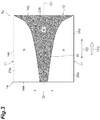
- FIG. 3 is a schematic view illustrating the second transfer column region. Although the second transfer column region 14A has the trapezoidal shape in plan view as described above, the second transfer column region 14A in FIG. 3 is schematically illustrated as a rectangular shape having a pair of short sides 14a and 14b and a pair of long sides 14c and 14d.
- the second transfer column region 14A includes a pair of first impurity regions 11 and a second impurity region 12.
- An impurity concentration of the second impurity region 12 is higher than an impurity concentration of the first impurity region 11. Configurations of the first impurity region 11 and the second impurity region 12 will be described later.
- the second impurity region 12 is provided from one short side 14a to the other short side 14b in the second direction D2 in the second transfer column region 14A.
- the second impurity region 12 is continuously provided from the short side 14a to the short side 14b.
- the short side 14a constitutes a part of the side 14g of the second region 14.
- the short side 14a is the one end of the second transfer column region 14A (second region 14) in the second direction D2.
- the short side 14a is positioned closer to the pixel region 3a in the second direction D2.
- the short side 14b constitutes a part of the side 14h of the second region 14.
- the short side 14b is the other end of the second transfer column region 14A (second region 14) in the second direction D2.
- the short side 14b is positioned closer to the shift register 9 in the second direction D2.
- the second impurity region 12 is positioned between the pair of first impurity regions 11 in the first direction D1.
- the second impurity region 12 has a shape that is line-symmetric with respect to a center line G1 of the second transfer column region 14A along the second direction D2 in plan view of FIG. 3 .
- a planar shape of the second impurity region 12 is line-symmetric with respect to the center line G1.
- the center line G1 is parallel to the pair of long sides 14c and 14d of the second transfer column region 14A and is positioned such that distances from the long sides 14c and 14d are equivalent.
- “equivalent” not only means that values are exactly the same, but also means that a difference in values is included in the range of a measurement error or a preset minute difference.
- planar shape of the second impurity region 12 is line-symmetric with respect to the center line G1 represents that regions, obtained by dividing the second impurity region 12 by the center line G1 and positioned with the center line G1 therebetween, are mirror-symmetric, and the regions has the same area and number.
- the center line G1 is a mirror symmetry axis.
- a width W of the second impurity region 12 in the first direction D1 increases in the direction from the short side 14a toward the short side 14b.
- the shape of the second impurity region 12 will be described later with reference to FIG. 5 .
- the second impurity region 12 forms an electrical potential gradient that increases in the positive X-axis direction of FIG. 1 in the second transfer column region 14A.
- the electrical potential gradient increases in the direction from the short side 14a to the short side 14b along the direction in which the pair of short sides 14a and 14b oppose each other, that is, along the second direction D2.
- This electrical potential gradient transfers a charge transferred from the photosensitive region 6 to the second transfer column region 14A in the direction from the short side 14a to the short side 14b in the second transfer column region 14A.
- the electrical potential gradient transfers the charge in the vertical transfer direction TD2.
- the charge that has reached the short side 14b is discharged from the second transfer column region 14A.
- each of the shift registers 9 is disposed such that the corresponding transfer section 7 is positioned between the corresponding pixel region 3a and the shift register 9.
- Each of the shift registers 9 is disposed near the long side of each of the pixel regions 3a.
- Each of the shift registers 9 is adjacent to the corresponding transfer section 7 in the second direction D2.
- the pixel region 3a, the transfer section 7, and the shift register 9 are distributed in the order of the pixel region 3a, the transfer section 7, and the shift register 9 in the second direction D2.
- the shift register 9 acquires the charge transferred from the transfer section 7, transfers the acquired charge in the horizontal transfer direction TD1 (negative Y-axis direction), and sequentially outputs the charge to the amplifier AM.
- the amplifier AM converts the charge output from the shift register 9 into a voltage, and outputs the converted voltage to the outside of the solid state imaging device 1 as an output of each of the photosensitive regions 6.
- the amplifier AM constitutes a read port.
- the shift register 9 includes a third region 15 and a fourth region 16.
- the third region 15 is disposed at a position corresponding to the first region 13.
- the fourth region 16 is disposed at a position corresponding to the second region 14.
- the third region 15 is disposed closer to the long side of the first region 13 in the second direction D2, and extends along the first direction D1.
- the third region 15 has a rectangular shape in plan view. This rectangular shape has a pair of short sides opposing each other in the first direction D1 and a pair of long sides opposing each other in the second direction D2.
- a width of the third region 15 in the first direction D1 is approximately the same as the width of the first region 13 in the first direction D1.
- the fourth region 16 is disposed closer to the side 14h of the second region 14 in the second direction D2.
- the fourth region 16 extends along a direction intersecting the first direction D1 and the second direction D2 such that an interval H between the fourth region 16 and the pixel region 3a in the second direction D2 increases in the horizontal transfer direction TD1 in response to a change in the length Lb.
- the fourth region 16 has a parallelogram shape in plan view. This parallelogram shape has a pair of short sides opposing each other in the first direction D1 and a pair of long sides opposing each other in the second direction D2.
- Each long side of the fourth region 16 is parallel to the side 14h of the second region 14. Each long side of the fourth region 16 extends linearly in such a manner as to intersect the first direction D1 and second direction D2 at a predetermined angle.
- a width of each long side of the fourth region 16 in the first direction D1 is larger than a width of each long side of the fourth region 16 in the second direction D2.
- An angle formed by each long side of the fourth region 16 with respect to the first direction D1 is smaller than an angle formed by each long side of the fourth region 16 with respect to the second direction D2.
- the fourth region 16 extends to be inclined such that the angle with respect to the first direction D1 is smaller than the angle with respect to the second direction D2.
- the fourth region 16 is inclined at a gentle angle closer to the first direction D1 (Y-axis direction) than to the second direction D2 (X-axis direction). For example, the fourth region 16 is inclined at an angle smaller than 45° with respect to the first direction D1.
- the width of the fourth region 16 in the first direction D1 is approximately the same as the width of the second region 14 in the first direction D1.
- a length of the fourth region 16 in the second direction D2 is approximately the same as a length of the third region 15 in the second direction D2.
- a width of the shift register 9 in the second direction D2 is approximately constant regardless of a position in the horizontal transfer direction TD1.
- Each of the amplifiers AM acquires a charge from a rear end in the horizontal transfer direction TD1 of the corresponding shift register 9, and outputs a voltage (signal) corresponding to the acquired charge.
- the amplifier AM is disposed in a region S.
- the region S is a region surrounded by the corresponding shift register 9 and the shift register 9 adjacent to the corresponding shift register 9 in the horizontal transfer direction TD1.
- the region S is also a region surrounded by the shift register 9 that transfers and outputs a charge generated in one pixel region 3a and the shift register 9 that transfers and outputs a charge generated in the other pixel region 3a, among two pixel regions 3a adjacent in the first direction D1.
- one amplifier AM is disposed in the region S and provided in one pixel region 3a.
- the solid state imaging device 1 includes the plurality of amplifiers AM for one light receiving region 3.
- one amplifier AM is provided for one pixel region 3a by being disposed in the region S.
- the solid state imaging device 1 is a multi-port solid state imaging device including a plurality of output sections (a plurality of read ports).
- Isolation regions are disposed between the photosensitive regions 6 adjacent in the first direction D1 and between the transfer sections 7 adjacent in the first direction D1.
- the isolation region disposed between the photosensitive regions 6 electrically isolates the adjacent photosensitive regions 6 from each other.
- the isolation region disposed between the transfer sections 7 electrically isolates the adjacent transfer sections 7 from each other.
- the solid state imaging device 1 includes a semiconductor substrate 10.
- the light receiving region 3, the plurality of transfer sections 7, and the plurality of shift registers 9 are formed on the semiconductor substrate 10.
- the semiconductor substrate 10 is a silicon substrate.
- the semiconductor substrate 10 includes a main part layer 10A serving as a base of the semiconductor substrate 10 and surface layers 24 to 26. The surface layers 24 to 26 are formed on one side of the main part layer 10A.
- the main part layer 10A is a p type semiconductor layer.
- the surface layer 24 is an n type semiconductor layer.
- the surface layer 25 includes a pair of n type semiconductor layers 25a and one n + type semiconductor layer 25b.
- the n + type semiconductor layer 25b is positioned between the pair of n type semiconductor layers 25a in the first direction D1.
- the surface layer 26 is an n - type semiconductor layer.
- the respective conductivity types of the p type and the n type may be switched so as to be opposite to the above-described conductivity types.
- a high impurity concentration is indicated by "+” attached to a conductivity type.
- the low impurity concentration also includes an aspect in which some impurities of a conductivity type attached with "-” are compensated with impurities of a conductivity type opposite to the conductivity type attached with "-” so that a low impurity concentration is obtained in appearance.
- the number of "+” indicates the degree of concentration of impurities of a conductivity type attached with "+”, and the larger number of "+” means a higher concentration of impurities of the conductivity type attached with "+”.
- the n type impurity is, for example, N, P, or As.
- the p type impurity is, for example, B or Al.
- a pn junction is formed at an interface between the main part layer 10A and the surface layer 24.
- the surface layer 24 constitutes the pixel region 3a.
- a plurality of electrodes 41 to 44 is disposed on an insulating layer (not illustrated).
- the electrodes 41 to 44 are formed on a region of the insulating layer corresponding to the surface layer 24.
- the electrodes 41 to 44 are indirectly disposed on the surface layer 24.
- the electrodes 41 to 44 are distributed in the order of the electrode 41, the electrode 42, the electrode 43, and the electrode 44 in the second direction D2.
- the electrodes 41 to 44 form a set, and a plurality of sets of electrodes 41 to 44 is disposed in the second direction D2.
- a region of the surface layer 24 positioned below the set of electrodes 41 to 44 constitutes one photosensitive region 6 (one pixel).
- a drive circuit applies signals P1V, P2V, P3V, and P4V to the electrodes 41 to 44, respectively.
- Each of the signals P1V, P2V, P3V, and P4V determines an electrical potential gradient of the region (photosensitive region 6) of the surface layer 24 positioned below the set of electrodes 41 to 44.
- the set of electrodes 41 to 44 forms an inclination of a potential that gradually becomes deeper in the vertical transfer direction TD2 in the region positioned below the set of electrodes 41 to 44.
- the set of electrodes 41 to 44 forms an electrical potential gradient that increases in the vertical transfer direction TD2.
- a charge generated in the photosensitive region 6 in response to incident light moves in the vertical transfer direction TD2 along the formed inclination of the potential.
- the drive circuit is controlled by a control device (not illustrated).
- the n type semiconductor layer 25a of the surface layer 25 constitutes the first impurity region 11 of the second transfer column region 14A.
- a shape of the first impurity region 11 corresponds to a shape of the n type semiconductor layer 25a.
- the n + type semiconductor layer 25b of the surface layer 25 constitutes the second impurity region 12 of the second transfer column region 14A.
- a shape of the second impurity region 12 corresponds to a shape of the n + type semiconductor layer 25b.
- An impurity concentration of the n + type semiconductor layer 25b is higher than an impurity concentration of the n type semiconductor layer 25a.
- a width W of the high n + type semiconductor layer 25b gradually increases in the vertical transfer direction TD2.
- the width W of the n + type semiconductor layer 25b is small in a region near the short side 14a in the vertical transfer direction TD2.
- an influence of fringing electric fields from the n type semiconductor layers 25a positioned on both sides of the n + type semiconductor layer 25b is large. Therefore, a potential of the surface layer 25 is shallow in the region near the short side 14a in the vertical transfer direction TD2.
- the width W of the n + type semiconductor layer 25b is large in a region near the short side 14b in the vertical transfer direction TD2.
- the width W of the n + type semiconductor layer 25b is large, the influence of fringing electric fields from the n type semiconductor layers 25a positioned on both sides of the n + type semiconductor layer 25b is small. Therefore, a potential of the surface layer 25 is deep in the region near the short side 14b in the vertical transfer direction TD2. Consequently, the surface layer 25 is formed with an inclination of a potential that gradually becomes deeper in the vertical transfer direction TD2 as illustrated in FIG. 4 .
- the surface layer 25 is formed with an electrical potential gradient that gradually increases in the vertical transfer direction TD2.
- FIG. 4 is a view illustrating a change in electrical potential formed in the solid state imaging device.
- An electrode 45 is also disposed on the insulating layer.
- the electrode 45 is formed on a region of the insulating layer corresponding to the surface layer 25.
- the electrode 45 is indirectly disposed on the surface layer 25.
- the surface layer 25 and the electrode 45 constitute the second transfer column region 14A (the second region 14 of the transfer section 7).
- the drive circuit gives a signal TG to the electrode 45.
- the potential of the surface layer 25 changes, for example, as illustrated in (a) and (b) of FIG. 4 . Due to the change of the potential, the second transfer column region 14A (the second region 14 of the transfer section 7) acquires a charge from the photosensitive region 6 and sends the acquired charge to the shift register 9.
- the first transfer column region 13A (the first region 13 of the transfer section 7) has a conventionally known configuration, the first transfer column region 13A is not illustrated.
- the first transfer column region 13A is constituted by, for example, a surface layer and an electrode that is indirectly disposed on the surface layer, which is similar to the conventional solid state imaging device. This surface layer does not include a plurality of impurity regions having different impurity concentrations.
- the surface layer is, for example, an n - type semiconductor layer.
- An electrode 46 is also disposed on the insulating layer.
- the electrode 46 is formed on a region of the insulating layer corresponding to the surface layer 26.
- the electrode 46 is indirectly disposed on the surface layer 26.
- the surface layer 26 and the electrode 46 constitute the shift register 9.
- the drive circuit gives a signal P1H to the electrode 46.
- the potential of the surface layer 26 changes, for example, as illustrated in (a) and (b) of FIG. 4 . Due to the change of the potential, the shift register 9 acquires a charge from the transfer section 7 and sends the acquired charge to the amplifier AM.
- the electrodes 41 to 46 are made of, for example, a polysilicon film.
- the above-described insulating layer is made of, for example, a silicon oxide film.
- FIG. 5 is a view used for describing the width of the second impurity region.
- FIG. 5 illustrates width W 1 , ..., W k , ..., and W n of the second impurity region 12 in sections L 1 , ..., L k , ..., and L n obtained by dividing the second transfer column region 14A into n sections in the second direction D2.
- the second transfer column region 14A has a length L in the second direction D2.
- n is an integer of two or more.
- k is an integer of two or more and n-1 or less.
- the width W 0 is the minimum width in the section L1.
- the width W 0 is the width of the second impurity region 12 at the most upstream end (the short side 14a illustrated in FIG. 3 ) in the vertical transfer direction TD2 in the second impurity region 12.
- each of the sections L 1 , ..., L k , ..., and L n is each of sections obtained by equally dividing the second transfer column region 14A into n sections in the second direction D2.
- the equal division means division into equal amounts
- each of the sections L 1 , ..., L k , ..., and L n is not necessarily divided to have the completely equal amount.
- the width of each of the sections L 1 , ..., L k , ..., and L n may include a measurement error or a minute difference within a preset range of about ⁇ several ⁇ m.
- the second transfer column region 14A is equally divided into twelve sections.
- Each of the widths W 1 , ..., W k , ..., and W n of the second impurity region 12 is, for example, a width at a position closest to the short side 14b (see FIG. 3 ) in each of the sections L 1 , ..., L k , ..., and L n .
- each of the widths W 1 , ..., W k , ..., and W n is a width at a downstream end in the vertical transfer direction TD2 in each of the sections L 1 , ..., L k , ..., and L n , and is the maximum width in each of the sections L 1 , ..., L k , ..., and L n .
- the widths W 1 , ..., W k , ..., and W n are not limited to the maximum widths in the respective sections L 1 , ..., L k , ..., and L n .
- each of the widths W 1 , ..., W k , ..., and W n may be an average value of widths in each of the sections L 1 , ..., L k , ..., and L n .
- the width W of the second impurity region 12 monotonously increases in the vertical transfer direction TD2 from the upstream end to the downstream end in the vertical transfer direction TD2.
- V 0 is an electrical potential of the second transfer column region 14A at the position of the width W 0 .
- FIG. 6 is a graph illustrating the electrical potential of the second impurity region for each notch width.
- the horizontal axis in FIG. 6 indicates the notch width [ ⁇ m].
- the vertical axis in FIG. 6 indicates the maximum electrical potential [V] of the second transfer column region 14A corresponding to the notch width.
- the vertical axis in FIG. 6 indicates that the maximum electrical potential increases in the upward direction, and the maximum electrical potential decreases in the downward direction.
- the electrical potential in the range corresponding to the range where the notch width is 0.8 ⁇ m to 6.1 ⁇ m is equally divided into n sections in the graph of FIG. 6 .
- the electrical potential is equally divided into twelve sections.
- the notch widths at the respective equally dividing points (1, ..., k, ... and n) of the electrical potential are read from the graph of FIG. 6 .
- the read notch widths at the respective equally dividing points are defined as the respective widths W 1 , ..., W k , ..., and W n of the second impurity region 12 corresponding to the respective equally dividing points.
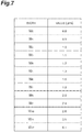
- FIG. 7 illustrates the widths W 0 , W 1 , ..., W k , ..., and W n of the obtained second impurity region 12.
- FIG. 7 is a table illustrating the width of the second impurity region at each equally dividing point.
- the shape of the second impurity region 12 is determined based on the obtained widths W 0 , W 1 , ..., W k , ..., and W n (see FIG. 7 ).
- the shape of the second impurity region 12 is determined by the above procedure.
- the shape of the second impurity region 12 is a shape similar to the shape illustrated in FIG. 5 regardless of the length of the second transfer column region 14A in the vertical transfer direction TD2.
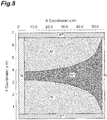
- FIG. 8 is a view illustrating a simulation model of the second transfer column region including the second impurity region according to the present embodiment.
- FIG. 9 is a graph illustrating a simulation result of a potential of the second transfer column region.
- the potential illustrated in FIG. 9 is a simulation result of the potential of the second transfer column region 14A using the model illustrated in FIG. 8 .
- the potential is indicated by an equipotential line.
- the positive x-axis direction in FIG. 9 corresponds to the vertical transfer direction TD2.
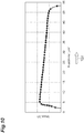
- FIG. 10 is a graph illustrating an electrical potential gradient in the transfer direction.
- FIG. 10 is a graph in which a value of an electrical potential corresponding to a position in the vertical transfer direction TD2 in the second transfer column region 14A is plotted based on the result of FIG. 9 .
- the horizontal axis in FIG. 10 indicates the position [ ⁇ m] in the vertical transfer direction TD2 (positive x-axis direction) of the second transfer column region 14A.
- the vertical axis in FIG. 10 indicates the maximum electrical potential [V] of the second transfer column region 14A.
- the vertical axis in FIG. 10 indicates that the maximum electrical potential decreases in the upward direction, and the maximum electrical potential increases in the downward direction.
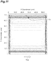
- FIG. 11 is a graph illustrating a simulation result of a potential of a second transfer column region according to a reference example. In the reference example, the second transfer column region 14A does not include the second impurity region 12.
- the second transfer column region 14A does not include the second impurity region 12 as illustrated in FIG. 11 , no electrical potential gradient is formed at the center of the second transfer column region 14A. Therefore, in a case in which the length of the second transfer column region 14A in the second direction D2 is long, for example, in a case in which the length of the second transfer column region 14A in the second direction D2 is about 50 ⁇ m, a charge Ec is not likely to be transferred in the vertical transfer direction TD2. In contrast, in a case in which the second transfer column region 14A includes the second impurity region 12 as illustrated in FIGS.
- the electrical potential gradient in the second transfer column region 14A is formed to be approximately constant over approximately the entire region along the vertical transfer direction TD2 of the second transfer column region 14A. In this case, the electrical potential gradient in the second transfer column region 14A efficiently transfers the charge Ec in the second transfer column region 14A.
- FIG. 12 is a schematic view illustrating the operation and effect of the solid state imaging device according to the present embodiment.
- a solid state imaging device 100 according to a comparative example is schematically illustrated.
- the solid state imaging device 1 of the present embodiment is schematically illustrated.
- the solid state imaging device 100 includes a transfer section 17 instead of the transfer section 7 of the present embodiment, and includes a shift register 19 instead of the shift register 9 of the present embodiment.
- the transfer section 17 has a length in the second direction D2 that gradually increases in the horizontal transfer direction TD1 in the entire transfer section 17.
- the transfer section 17 is positioned between the pixel region 3a and the shift register 9 in the second direction D2. In the entire region of the transfer section 17 in the first direction D1, an interval between the pixel region 3a and the shift register 19 gradually increases in the horizontal transfer direction TD1. Therefore, a charge transfer distance along the second direction D2 from the pixel region 3a to the shift register 9 becomes long.
- the entire shift register 19 extends along a direction intersecting the first direction D1 and the second direction D2. In this case, a charge that tries to move in the horizontal transfer direction TD1 is transferred while hitting a boundary with the transfer section 17 in the shift register 19. Therefore, charge transfer efficiency in the shift register 9 may deteriorate due to inhibition by a potential of the transfer section 17.
- the transfer section 7 includes the first region 13 including the plurality of first transfer column regions 13A and the second region 14 including the plurality of second transfer column regions 14A.
- the charge transfer distance along the second direction D2 is short as compared with each of the second transfer column regions 14A. Therefore, the charge transfer distance along the second direction D2 is short in the solid state imaging device 1 as compared with the comparative example in which the length in the second direction D2 of all the transfer column regions 7a included in the transfer section 7 gradually increases in the horizontal transfer direction TD1.
- the shift register 9 includes the third region 15 and the fourth region 16.
- a charge that tries to move in the horizontal transfer direction TD1 tends not to hit the boundary with the transfer section 7 in the shift register 9. Therefore, the charge transfer in the shift register 9 tends not to be inhibited by the potential of the transfer section 7.
- the solid state imaging device 1 improves the charge transfer efficiency in the shift register 9 as compared with the comparative example in which the entire shift register 9 extends along the direction intersecting the first direction D1 and the second direction D2.
- the solid state imaging device 1 improves the charge transfer efficiency.
- each long side of the fourth region 16 extends linearly to intersect the first direction D1 and second direction D2 at the predetermined angle.
- the charge transfer in the shift register 9 tends not to be inhibited by the potential of the transfer section 7 even in a case in which the charge hits the boundary with the transfer section 7 in the shift register 9 in the fourth region 16, for example, as compared with a configuration in which each long side of the fourth region 16 is bent in a staircase shape.
- the fourth region 16 is inclined at the gentle angle closer to the first direction D1 than to the second direction D2.
- the charge transfer in the shift register 9 tends not to be inhibited by the potential of the transfer section 7 even in a case in which the charge hits the boundary with the transfer section 7 in the shift register 9 in the fourth region 16, for example, as compared with a configuration in which the fourth region 16 is inclined at an angle larger than 45° with respect to the first direction D1.
- the solid state imaging device 1 controls deterioration in charge transfer efficiency even in a case in which the charge hits the boundary with the shift register 9 in the transfer section 7.
- each of the second transfer column regions 14A includes the first impurity region 11 and the second impurity region 12. Since the width W of the second impurity region 12 in the first direction D1 increases in the vertical transfer direction TD2, the electrical potential gradient in which the electrical potential increases in the vertical transfer direction TD2 is formed in each of the second transfer column regions 14A. Therefore, each of the second transfer column regions 14A having a long charge transfer distance from the pixel region 3a to the shift register 9 also efficiently transfers the charge due to this electrical potential gradient.
- the widths W 1 , ..., W k , ..., and W n of the second impurity region 12 in the respective sections L 1 , ..., L k , ..., and L n are set such that the electrical potential difference of the second impurity region 12 between the adjacent sections among the sections L 1 , ..., L k , ..., and L n is constant.
- the electrical potential gradient in the second transfer column region 14A is approximately constant. Therefore, the second transfer column region 14A transfers the charge more efficiently.
- the solid state imaging device 1 ensures the region S surrounded by the corresponding shift register 9 and the shift register 9 adjacent to the corresponding shift register 9 in the horizontal transfer direction TD1.
- the amplifier AM that is arranged to output the signal corresponding to the charge acquired from the corresponding shift register 9 is disposed. Therefore, the charge transfer direction tends not to be bent from the shift register 9 toward the amplifier AM in the solid state imaging device 1.
- the configuration in which the amplifier AM is disposed in the region S improves the charge transfer efficiency and facilitates the design of the solid state imaging device 1.
- the shape of the second impurity region 12 is not limited to the shape illustrated in the above embodiment.
- the second impurity region 12 can have various shapes as illustrated in FIG. 13.
- FIG. 13 is a schematic view illustrating modifications of the second impurity region.
- a boundary position of each of sections obtained by dividing the second transfer column region 14A into a plurality of sections is indicated by a two-dot chain line.
- the second impurity region 12 is provided from the short side 14a to the short side 14b in the second transfer column region 14A.
- the second impurity region 12 is not necessarily provided from the short side 14a in the second transfer column region 14A.
- the second impurity region 12A is provided from a vicinity of the short side 14a to the short side 14b.
- the vicinity of the short side 14a means, for example, a position away from the short side 14a to such an extent that movement of a charge is not hindered.
- the vicinity of the short side 14a is a position separated by about several ⁇ m from the short side 14a.
- the vicinity of the short side 14a is a position closer to the short side 14b than the short side 14a in the section L 1 , which is the closest to the short side 14a among the sections L 1 , ..., L k , ..., and L n .
- each of the sections L 1 , ..., L k , ..., and L n is each of the sections obtained by equally dividing the second transfer column region 14A into n sections, and the widths of the respective sections L 1 , ..., L k , ..., and L n in the second direction D2 are equivalent.
- the widths of the respective sections L 1 , ..., L k , ..., and L n in the second direction D2 are not necessarily equivalent.
- each of the sections is, for example, each of sections obtained by dividing the second transfer column region 14A such that a width in the second direction D2 becomes gradually narrower in the vertical transfer direction TD2. Even in this case, an increase rate of a width of a second impurity region 12B in each of the sections becomes gradually larger in the transfer direction TD.
- the width W of the second impurity region 12 increases within each of the sections L 1 , ..., L k , ..., and L n .
- the width W of the second impurity region 12 does not necessarily increase within each of the sections L 1 , ..., L k , ..., and L n .
- a width W of a second impurity region 12C does not increase within each section, but increases at a boundary position of each of the sections.
- An outer shape of the second impurity region 12C within each of the sections is a rectangle.
- the second impurity region 12 is constituted by one region.
- the second impurity region 12 may be constituted by a plurality of minute regions.
- the second impurity region 12D is constituted by a plurality of minute regions 12d in each section.
- an outline of a region corresponding to the second impurity region 12D is indicated by a broken line.
- an increase rate of the width W n of the second impurity region 12 may change so as to increase near the short side 14b.
- the second transfer column region 14A is equally divided into three sections.
- an increase rate of a width of the second impurity region 12E is not constant but changes so as to become larger near the short side 14b.
- the second transfer column region 14A may be equally divided into two sections or may be equally divided into four or more sections.
- Near the short side 14b means, for example, to be closer to the short side 14b than the center line CL in the second direction D2 in the section that is the closest to the short side 14b.
- the second transfer column regions 14A does not necessarily include a plurality of impurity regions having different impurity concentrations.
- the second transfer column region 14A does not necessarily include the second impurity region 12.
- the present invention can be used for a multi-port CCD image sensor.
Landscapes
- Engineering & Computer Science (AREA)
- Multimedia (AREA)
- Signal Processing (AREA)
- Solid State Image Pick-Up Elements (AREA)
- Transforming Light Signals Into Electric Signals (AREA)
Abstract
Description
- The present invention relates to a solid state imaging device.
- Known solid state imaging devices include a plurality of pixel regions, a plurality of first transfer sections, and a plurality of second transfer sections (for example, see Patent Literature 1). The plurality of pixel regions respectively include a plurality of photosensitive regions that are two-dimensionally arrayed in a first direction and a second direction orthogonal to the first direction, and are distributed in the first direction. Each of the first transfer sections is distributed with the corresponding pixel region of the plurality of pixel regions in the second direction, and transfers a charge generated in the photosensitive region for each corresponding pixel region. Each of the second transfer sections is distributed with the corresponding first transfer section of the plurality of first transfer sections in the second direction, and acquires a charge transferred from the corresponding first transfer section. Each of the second transfer sections transfers the acquired charge in the first direction.
- Patent Literature 1: Japanese Unexamined Patent Publication No.
2000-350100 - There is a case where one solid state imaging device includes a plurality of read ports in order to increase a frame rate in a solid state imaging device. In this case, for example, it is necessary to secure a space to dispose an amplifier for each read port. In the solid state imaging device described in
Patent Literature 1, a length of the first transfer section in the second direction gradually increases in a charge transfer direction in the second transfer section corresponding to the first transfer section. The second transfer section corresponding to the first transfer section extends along a direction intersecting the first direction and the second direction such that a distance from the pixel region becomes gradually longer in the charge transfer direction. The amplifier is disposed in a space between the second transfer sections adjacent in the first direction. - In the solid state imaging device described in
Patent Literature 1, the length in the second direction gradually increases in the charge transfer direction in the second transfer section in the entire range of the first transfer section in the first direction. The first transfer section is positioned between the pixel region and the second transfer section in the second direction. In the entire range of the first transfer section in the first direction, the distance between the pixel region and the second transfer section gradually increases in the charge transfer direction in the second transfer section. Therefore, a charge transfer distance along the second direction from the pixel region to the second transfer section becomes long. The entire second transfer section extends along a direction intersecting the first direction and the second direction. In this case, the charge that tries to move in the charge transfer direction along the first direction is transferred while hitting a boundary with the first transfer section in the second transfer section. Therefore, charge transfer efficiency in the second transfer section may deteriorate due to inhibition by a potential of the first transfer section. - An object of one aspect of the present invention is to provide a solid state imaging device that improves charge transfer efficiency.
- One aspect of the present invention is a solid state imaging device including a plurality of pixel regions, a plurality of first transfer sections, and a plurality of second transfer sections. The plurality of pixel regions each includes a plurality of photosensitive regions that is two-dimensionally arrayed in a first direction and a second direction orthogonal to the first direction, and is distributed in the first direction. Each of the plurality of first transfer sections is distributed with a corresponding pixel region of the plurality of pixel regions in the second direction, and is arranged to transfer a charge generated in the photosensitive region for each corresponding pixel region. Each of the plurality of second transfer sections is distributed with a corresponding first transfer section of the plurality of first transfer sections in the second direction, is arranged to acquire a charge transferred from the corresponding first transfer section, and is arranged to transfer the acquired charge in the first direction. Each of the first transfer sections includes a first region including a plurality of first transfer column regions distributed in the first direction; and a second region including a plurality of second transfer column regions distributed in the first direction. The second region is positioned downstream of the first region in the charge transfer direction in the second transfer section. Lengths in the second direction of the plurality of first transfer column regions are equal. Lengths in the second direction of the plurality of second transfer column regions are longer than the length of the first transfer column region, and increase as the second transfer column region is positioned downstream in the charge transfer direction. Each of the second transfer sections includes a third region disposed to correspond to the first region and a fourth region disposed to correspond to the second region. The third region extends along the first direction. The fourth region extends along a direction intersecting the first direction and the second direction such that an interval between the fourth region and the pixel region in the second direction increases in the charge transfer direction in response to a change in the lengths of the plurality of second transfer column regions.
- In the one aspect, a charge transfer distance along the second direction in each of the first transfer column regions is shorter than a charge transfer distance along the second direction in each of the second transfer column regions. Therefore, the charge transfer distance along the second direction is short in the one aspect as compared with a configuration in which the length in the second direction of the entire transfer column region included in the first transfer section gradually increases in the charge transfer direction in the second transfer section.
- In the third region of the above aspect, a charge that tries to move in the charge transfer direction along the first direction tends not to hit a boundary with the first transfer section in the second transfer section. Therefore, the charge transfer in the second transfer section tends not to be inhibited by a potential of the first transfer section. The one aspect improves charge transfer efficiency in the second transfer section as compared with a configuration in which an entire second transfer section extends along the direction intersecting the first direction and the second direction.
- As described above, the solid state imaging device according to the one aspect improves charge transfer efficiency.
- In the one aspect, each of the second transfer column regions may include a first impurity region and a second impurity region having a higher impurity concentration than that of the first impurity region. In each of the second transfer column regions, the second impurity region may be provided from one end positioned closer to the pixel region in the second direction or a vicinity of the one end to another end closer to the second transfer section. A width of the second impurity region in the first direction may increase in a vertical transfer direction from the one end to the other end. In a case in which the width of the second impurity region in the first direction increases in the vertical transfer direction, an electrical potential gradient in which an electrical potential increases in the vertical transfer direction is formed in each of the second transfer column regions. Therefore, each of the second transfer column regions having a long charge transfer distance from the pixel region to the second transfer section also efficiently transfers the charge due to this electrical potential gradient.
- In the one aspect, the width of the second impurity region in each section, obtained by dividing the second transfer column region into n sections in the second direction, may be set such that an electrical potential difference of the second impurity region between adjacent sections is constant. In this case, n is an integer of two or more. In this configuration, the electrical potential gradient in the second transfer column region is approximately constant. Therefore, the second transfer column region transfers the charge more efficiently.
- The one aspect may further include a plurality of output sections. In this case, the plurality of output sections is arranged to acquire a charge from a rear end in the charge transfer direction of a corresponding second transfer section of the plurality of second transfer sections, and to output a signal corresponding to the acquired charge. The output section may be disposed in a region surrounded by the corresponding second transfer section and the second transfer section adjacent to the corresponding second transfer section in the charge transfer direction. Even in a case in which a width of the second transfer section in the first direction is not smaller than a width of the pixel region in the first direction, this configuration ensures the region surrounded by the corresponding second transfer section and the second transfer section adjacent to the corresponding second transfer section in the charge transfer direction. The output section that outputs the signal corresponding to the charge acquired from the corresponding second transfer section is disposed in this region. Therefore, the charge transfer direction tends not to bends from the second transfer section toward the output section in this configuration. This configuration improves the charge transfer efficiency and facilitates a design of the solid state imaging device.
- According to one aspect of the present invention, the solid state imaging device that improves the charge transfer efficiency is provided.
-
-
FIG. 1 is a view illustrating a planar configuration of a solid state imaging device. -
FIG. 2 is a view illustrating a cross-sectional configuration of the solid state imaging device. -
FIG. 3 is a schematic view illustrating a second transfer column region. -
FIG. 4 is a view illustrating a change in electrical potential formed in the solid state imaging device. -
FIG. 5 is a view used for describing a width of a second impurity region. -
FIG. 6 is a graph illustrating an electrical potential of the second impurity region for each notch width. -
FIG. 7 is a table illustrating a width of the second impurity region at each equally dividing point. -
FIG. 8 is a view illustrating a simulation model of the second transfer column region including the second impurity region according to the present embodiment. -
FIG. 9 is a graph illustrating a simulation result of a potential of the second transfer column region. -
FIG. 10 is a graph illustrating an electrical potential gradient in a transfer direction. -
FIG. 11 is a graph illustrating a simulation result of a potential of a second transfer column region according to a reference example. -
FIG. 12 is a schematic view illustrating an operation and an effect of the solid state imaging device according to the present embodiment. -
FIG. 13 is a schematic view illustrating modifications of the second impurity region. - Hereinafter, embodiments of the present invention will be described in detail with reference to the accompanying drawings. The same reference signs will be used for the same elements or elements having the same functions in the description, and redundant descriptions will be omitted.
- First, a configuration of a solid
state imaging device 1 according to the present embodiment will be described with reference toFIGS. 1 and2 .FIG. 1 is a view illustrating a planar configuration of the solid state imaging device.FIG. 2 is a view illustrating a cross-sectional configuration of the solid state imaging device.FIG. 2 illustrates the cross-sectional configuration of the solid state imaging device taken along line II-II inFIG. 1 . - As illustrated in
FIG. 1 , the solidstate imaging device 1 includes a plurality ofpixel regions 3a, a plurality oftransfer sections 7, a plurality ofshift registers 9, and a plurality of amplifiers AM. In the present embodiment, for example, thetransfer section 7 includes a first transfer section, theshift register 9 includes a second transfer section, and the amplifier AM includes an output section. - The
pixel region 3a has a rectangular shape in plan view. The rectangular shape has, for example, a pair of short sides opposing each other in a first direction D1 and a pair of long sides opposing each other in a second direction D2. In the present embodiment, the first direction D1 includes both a positive direction and a negative direction along the Y axis. The second direction D2 includes both a positive direction and a negative direction along the X axis. The first direction D1 and the second direction D2 are orthogonal to each other. The plurality ofpixel regions 3a is distributed in the first direction D1. The plurality ofpixel regions 3a constitutes alight receiving region 3. Thelight receiving region 3 includes the plurality ofpixel regions 3a. Thelight receiving region 3 is divided into the plurality ofpixel regions 3a in the first direction D1. - The
pixel region 3a includes a plurality ofphotoelectric converters 5. The plurality ofphotoelectric converters 5 is two-dimensionally arrayed in the first direction D1 and the second direction D2. Each of thephotoelectric converters 5 includes aphotosensitive region 6 that generates a charge in response to incident light. In the present embodiment, onephotoelectric converter 5 includes onephotosensitive region 6. Thephotosensitive regions 6 are two-dimensionally arrayed in the first direction D1 and the second direction D2. One photosensitive region 6 (photoelectric converter 5) forms one pixel in thepixel region 3a. Each of thepixel regions 3a includes the plurality ofphotosensitive regions 6 which are two-dimensionally arrayed. - The plurality of
transfer sections 7 correspond to the plurality ofpixel regions 3a, respectively. Each of thetransfer sections 7 is disposed to be adjacent to the long side of acorresponding pixel region 3a of the plurality ofpixel regions 3a. Each of thetransfer sections 7 is disposed in the second direction D2 to be adjacent to the long side of thecorresponding pixel region 3a and distributed with the correspondingpixel region 3a. Thetransfer section 7 is positioned between thepixel region 3a and theshift register 9. Thetransfer section 7 transfers a charge generated in aphotosensitive region 6 of thecorresponding pixel region 3a. Thetransfer section 7 acquires the charge discharged from thepixel region 3a and transfers the acquired charge to theshift register 9. - Each of the
transfer sections 7 includes a plurality oftransfer column regions 7a. The plurality oftransfer column regions 7a is distributed in the first direction D1 to correspond to columns of thephotosensitive regions 6 distributed in the first direction D1, that is, correspond to pixel columns. Thetransfer column region 7a transfers a charge generated in thephotosensitive region 6 of the corresponding pixel column. Thetransfer column region 7a acquires the charge from the corresponding pixel column and transfers the acquired charge to theshift register 9. - Each of the
transfer sections 7 includes afirst region 13 and asecond region 14. Thesecond region 14 is positioned downstream of thefirst region 13 in a charge transfer direction in thecorresponding shift register 9. In the present embodiment, the charge transfer direction in theshift register 9 means a direction from thefirst region 13 toward thesecond region 14 along the first direction D1. In the present embodiment, the charge transfer direction in theshift register 9 is the negative Y-axis direction. Hereinafter, the charge transfer direction in theshift register 9 is referred to as a "horizontal transfer direction TD1". A downstream in the horizontal transfer direction TD1 means that the order of charge transfer in the charge transfer direction is late. Thefirst region 13 is positioned upstream of thesecond region 14 in the horizontal transfer direction TD1, and thesecond region 14 is positioned downstream of thefirst region 13 in the horizontal transfer direction TD1. - In the
first region 13, thetransfer column region 7a includes firsttransfer column regions 13A. Therefore, each of thefirst regions 13 includes the plurality of firsttransfer column regions 13A. Lengths La of the respective firsttransfer column regions 13A in the second direction D2 are equal. In the present embodiment, the expression that the lengths La are equal means not only that values are exactly the same but also that a difference in the values is included in a measurement error or a preset range of about ± 1 µm. In each of thefirst regions 13, the lengths La of the plurality of firsttransfer column regions 13A are equal, and the plurality of firsttransfer column regions 13A are distributed in the first direction D1. Therefore, each of thefirst regions 13 has a rectangular shape in plan view. This rectangular shape has a pair of short sides opposing each other in the first direction D1 and a pair of long sides opposing each other in the second direction D2. The length La is, for example, 7 µm. - In the
second region 14, thetransfer column region 7a includes secondtransfer column regions 14A. Therefore, each of thesecond regions 14 includes the plurality of secondtransfer column regions 14A. Lengths Lb of the respective secondtransfer column regions 14A in the second direction D2 are longer than the length La. The lengths Lb increase as the secondtransfer column region 14A is positioned downstream in the horizontal transfer direction TD1. In thesecond region 14, the trapezoidal secondtransfer column regions 14A are distributed in the first direction D1 such that the lengths Lb increase as the secondtransfer column region 14A is positioned downstream in the horizontal transfer direction TD1. Therefore, thesecond region 14 has a trapezoidal shape in plan view. This trapezoidal shape has a pair ofsides sides side 14e toward theside 14f. - Sides, adjacent to the
pixel region 3a, of the respective secondtransfer column regions 14A are distributed in a straight line in the first direction D1. The sides, adjacent to thepixel region 3a, of the respective secondtransfer column regions 14A constitute theside 14g of thesecond region 14. Theside 14g extends linearly in the first direction D1. Sides, adjacent to theshift register 9, of the respective secondtransfer column regions 14A are a distributed in a straight line in such a manner as to intersect the first direction D1 and the second direction D2 at the same angle. The sides, adjacent to theshift register 9, of the respective secondtransfer column regions 14A constitute theside 14h of thesecond region 14. Theside 14h extends linearly to intersect the first direction D1 and the second direction D2 at a predetermined angle. - The length Lb becomes the maximum at a position of the
side 14f. The maximum value of the length Lb is, for example, 50 µm. The maximum length of thesecond region 14 in the second direction D2, that is, the length of theside 14f is longer than a sum of lengths in the second direction D2 of thefirst region 13 andshift register 9 that are adjacent in the first direction D1 to the secondtransfer column region 14A positioned most downstream in the horizontal transfer direction TD1 in thesecond region 14. The length of theside 14f is longer than the sum of the length La and the length of theshift register 9 in the second direction D2. - The
side 14e is one end of thesecond region 14 in the first direction D1. Theside 14e is positioned closer to thefirst region 13 in the first direction D1. Theside 14f is another end of thesecond region 14 in the first direction D1. Theside 14f is positioned opposite to thefirst region 13 in the first direction D1. Theside 14g is one end of thesecond region 14 in the second direction D2. Theside 14g is positioned closer to thepixel region 3a in the second direction D2. Theside 14h is another end of thesecond region 14 in the second direction D2. Theside 14h is positioned closer to theshift register 9 in the second direction D2. Hereinafter, a direction from thepixel region 3a to theshift register 9 along the direction from theside 14g toward theside 14h, that is, along the second direction D2, is referred to as a "vertical transfer direction TD2". - A width of the
first region 13 in the first direction D1 is larger than a width of thesecond region 14 in the first direction D1. The number of the firsttransfer column regions 13A distributed in the first direction D1 is larger than the number of the secondtransfer column regions 14A distributed in the first direction D1. For example, the width of thefirst region 13 in the first direction D1 is about 10 times the width of thesecond region 14 in the first direction D1. In this case, a ratio between the number of the firsttransfer column regions 13A and the number of the secondtransfer column regions 14A is about 10 : 1. - Each of the second
transfer column regions 14A includes a plurality of impurity regions having different impurity concentrations.FIG. 3 is a schematic view illustrating the second transfer column region. Although the secondtransfer column region 14A has the trapezoidal shape in plan view as described above, the secondtransfer column region 14A inFIG. 3 is schematically illustrated as a rectangular shape having a pair ofshort sides long sides - As illustrated in
FIG. 3 , the secondtransfer column region 14A includes a pair offirst impurity regions 11 and asecond impurity region 12. An impurity concentration of thesecond impurity region 12 is higher than an impurity concentration of thefirst impurity region 11. Configurations of thefirst impurity region 11 and thesecond impurity region 12 will be described later. - The
second impurity region 12 is provided from oneshort side 14a to the othershort side 14b in the second direction D2 in the secondtransfer column region 14A. In the present embodiment, thesecond impurity region 12 is continuously provided from theshort side 14a to theshort side 14b. Theshort side 14a constitutes a part of theside 14g of thesecond region 14. Theshort side 14a is the one end of the secondtransfer column region 14A (second region 14) in the second direction D2. Theshort side 14a is positioned closer to thepixel region 3a in the second direction D2. Theshort side 14b constitutes a part of theside 14h of thesecond region 14. Theshort side 14b is the other end of the secondtransfer column region 14A (second region 14) in the second direction D2. Theshort side 14b is positioned closer to theshift register 9 in the second direction D2. Thesecond impurity region 12 is positioned between the pair offirst impurity regions 11 in the first direction D1. - The
second impurity region 12 has a shape that is line-symmetric with respect to a center line G1 of the secondtransfer column region 14A along the second direction D2 in plan view ofFIG. 3 . InFIG. 3 , a planar shape of thesecond impurity region 12 is line-symmetric with respect to the center line G1. The center line G1 is parallel to the pair oflong sides transfer column region 14A and is positioned such that distances from thelong sides second impurity region 12 is line-symmetric with respect to the center line G1 represents that regions, obtained by dividing thesecond impurity region 12 by the center line G1 and positioned with the center line G1 therebetween, are mirror-symmetric, and the regions has the same area and number. The center line G1 is a mirror symmetry axis. - A width W of the
second impurity region 12 in the first direction D1 increases in the direction from theshort side 14a toward theshort side 14b. The shape of thesecond impurity region 12 will be described later with reference toFIG. 5 . - The
second impurity region 12 forms an electrical potential gradient that increases in the positive X-axis direction ofFIG. 1 in the secondtransfer column region 14A. The electrical potential gradient increases in the direction from theshort side 14a to theshort side 14b along the direction in which the pair ofshort sides photosensitive region 6 to the secondtransfer column region 14A in the direction from theshort side 14a to theshort side 14b in the secondtransfer column region 14A. The electrical potential gradient transfers the charge in the vertical transfer direction TD2. The charge that has reached theshort side 14b is discharged from the secondtransfer column region 14A. - As illustrated in
FIG. 1 , each of the shift registers 9 is disposed such that thecorresponding transfer section 7 is positioned between thecorresponding pixel region 3a and theshift register 9. Each of the shift registers 9 is disposed near the long side of each of thepixel regions 3a. Each of the shift registers 9 is adjacent to thecorresponding transfer section 7 in the second direction D2. Thepixel region 3a, thetransfer section 7, and theshift register 9 are distributed in the order of thepixel region 3a, thetransfer section 7, and theshift register 9 in the second direction D2. Theshift register 9 acquires the charge transferred from thetransfer section 7, transfers the acquired charge in the horizontal transfer direction TD1 (negative Y-axis direction), and sequentially outputs the charge to the amplifier AM. The amplifier AM converts the charge output from theshift register 9 into a voltage, and outputs the converted voltage to the outside of the solidstate imaging device 1 as an output of each of thephotosensitive regions 6. The amplifier AM constitutes a read port. - The
shift register 9 includes athird region 15 and afourth region 16. Thethird region 15 is disposed at a position corresponding to thefirst region 13. Thefourth region 16 is disposed at a position corresponding to thesecond region 14. Thethird region 15 is disposed closer to the long side of thefirst region 13 in the second direction D2, and extends along the first direction D1. Thethird region 15 has a rectangular shape in plan view. This rectangular shape has a pair of short sides opposing each other in the first direction D1 and a pair of long sides opposing each other in the second direction D2. In the present embodiment, a width of thethird region 15 in the first direction D1 is approximately the same as the width of thefirst region 13 in the first direction D1. - The
fourth region 16 is disposed closer to theside 14h of thesecond region 14 in the second direction D2. Thefourth region 16 extends along a direction intersecting the first direction D1 and the second direction D2 such that an interval H between thefourth region 16 and thepixel region 3a in the second direction D2 increases in the horizontal transfer direction TD1 in response to a change in the length Lb. Thefourth region 16 has a parallelogram shape in plan view. This parallelogram shape has a pair of short sides opposing each other in the first direction D1 and a pair of long sides opposing each other in the second direction D2. - Each long side of the
fourth region 16 is parallel to theside 14h of thesecond region 14. Each long side of thefourth region 16 extends linearly in such a manner as to intersect the first direction D1 and second direction D2 at a predetermined angle. A width of each long side of thefourth region 16 in the first direction D1 is larger than a width of each long side of thefourth region 16 in the second direction D2. An angle formed by each long side of thefourth region 16 with respect to the first direction D1 is smaller than an angle formed by each long side of thefourth region 16 with respect to the second direction D2. Thefourth region 16 extends to be inclined such that the angle with respect to the first direction D1 is smaller than the angle with respect to the second direction D2. Thefourth region 16 is inclined at a gentle angle closer to the first direction D1 (Y-axis direction) than to the second direction D2 (X-axis direction). For example, thefourth region 16 is inclined at an angle smaller than 45° with respect to the first direction D1. - The width of the
fourth region 16 in the first direction D1 is approximately the same as the width of thesecond region 14 in the first direction D1. A length of thefourth region 16 in the second direction D2 is approximately the same as a length of thethird region 15 in the second direction D2. A width of theshift register 9 in the second direction D2 is approximately constant regardless of a position in the horizontal transfer direction TD1. - Each of the amplifiers AM acquires a charge from a rear end in the horizontal transfer direction TD1 of the
corresponding shift register 9, and outputs a voltage (signal) corresponding to the acquired charge. The amplifier AM is disposed in a region S. The region S is a region surrounded by thecorresponding shift register 9 and theshift register 9 adjacent to thecorresponding shift register 9 in the horizontal transfer direction TD1. The region S is also a region surrounded by theshift register 9 that transfers and outputs a charge generated in onepixel region 3a and theshift register 9 that transfers and outputs a charge generated in theother pixel region 3a, among twopixel regions 3a adjacent in the first direction D1. In the present embodiment, one amplifier AM is disposed in the region S and provided in onepixel region 3a. The solidstate imaging device 1 includes the plurality of amplifiers AM for onelight receiving region 3. In the solidstate imaging device 1, one amplifier AM is provided for onepixel region 3a by being disposed in the region S. The solidstate imaging device 1 is a multi-port solid state imaging device including a plurality of output sections (a plurality of read ports). - Isolation regions are disposed between the
photosensitive regions 6 adjacent in the first direction D1 and between thetransfer sections 7 adjacent in the first direction D1. The isolation region disposed between thephotosensitive regions 6 electrically isolates the adjacentphotosensitive regions 6 from each other. The isolation region disposed between thetransfer sections 7 electrically isolates theadjacent transfer sections 7 from each other. - The solid
state imaging device 1 includes asemiconductor substrate 10. Thelight receiving region 3, the plurality oftransfer sections 7, and the plurality ofshift registers 9 are formed on thesemiconductor substrate 10. In the present embodiment, thesemiconductor substrate 10 is a silicon substrate. As illustrated inFIG. 2 , thesemiconductor substrate 10 includes amain part layer 10A serving as a base of thesemiconductor substrate 10 and surface layers 24 to 26. The surface layers 24 to 26 are formed on one side of themain part layer 10A. - The
main part layer 10A is a p type semiconductor layer. Thesurface layer 24 is an n type semiconductor layer. As illustrated inFIG. 3 , thesurface layer 25 includes a pair of ntype semiconductor layers 25a and one n+type semiconductor layer 25b. The n+type semiconductor layer 25b is positioned between the pair of ntype semiconductor layers 25a in the first direction D1. Thesurface layer 26 is an n- type semiconductor layer. The respective conductivity types of the p type and the n type may be switched so as to be opposite to the above-described conductivity types. - A high impurity concentration is indicated by "+" attached to a conductivity type. A low impurity concentration indicated by "-" attached to a conductivity type. The low impurity concentration also includes an aspect in which some impurities of a conductivity type attached with "-" are compensated with impurities of a conductivity type opposite to the conductivity type attached with "-" so that a low impurity concentration is obtained in appearance. The number of "+" indicates the degree of concentration of impurities of a conductivity type attached with "+", and the larger number of "+" means a higher concentration of impurities of the conductivity type attached with "+". The n type impurity is, for example, N, P, or As. The p type impurity is, for example, B or Al.
- A pn junction is formed at an interface between the
main part layer 10A and thesurface layer 24. Thesurface layer 24 constitutes thepixel region 3a. A plurality ofelectrodes 41 to 44 is disposed on an insulating layer (not illustrated). Theelectrodes 41 to 44 are formed on a region of the insulating layer corresponding to thesurface layer 24. Theelectrodes 41 to 44 are indirectly disposed on thesurface layer 24. Theelectrodes 41 to 44 are distributed in the order of theelectrode 41, theelectrode 42, theelectrode 43, and theelectrode 44 in the second direction D2. Theelectrodes 41 to 44 form a set, and a plurality of sets ofelectrodes 41 to 44 is disposed in the second direction D2. A region of thesurface layer 24 positioned below the set ofelectrodes 41 to 44 constitutes one photosensitive region 6 (one pixel). - A drive circuit (not illustrated) applies signals P1V, P2V, P3V, and P4V to the
electrodes 41 to 44, respectively. Each of the signals P1V, P2V, P3V, and P4V determines an electrical potential gradient of the region (photosensitive region 6) of thesurface layer 24 positioned below the set ofelectrodes 41 to 44. The set ofelectrodes 41 to 44 forms an inclination of a potential that gradually becomes deeper in the vertical transfer direction TD2 in the region positioned below the set ofelectrodes 41 to 44. The set ofelectrodes 41 to 44 forms an electrical potential gradient that increases in the vertical transfer direction TD2. A charge generated in thephotosensitive region 6 in response to incident light moves in the vertical transfer direction TD2 along the formed inclination of the potential. The drive circuit is controlled by a control device (not illustrated). - As illustrated in
FIG. 3 , the ntype semiconductor layer 25a of thesurface layer 25 constitutes thefirst impurity region 11 of the secondtransfer column region 14A. A shape of thefirst impurity region 11 corresponds to a shape of the ntype semiconductor layer 25a. The n+type semiconductor layer 25b of thesurface layer 25 constitutes thesecond impurity region 12 of the secondtransfer column region 14A. A shape of thesecond impurity region 12 corresponds to a shape of the n+type semiconductor layer 25b. - An impurity concentration of the n+
type semiconductor layer 25b is higher than an impurity concentration of the ntype semiconductor layer 25a. A width W of the high n+type semiconductor layer 25b gradually increases in the vertical transfer direction TD2. The width W of the n+type semiconductor layer 25b is small in a region near theshort side 14a in the vertical transfer direction TD2. In a case in which the width W of the n+type semiconductor layer 25b is small, an influence of fringing electric fields from the ntype semiconductor layers 25a positioned on both sides of the n+type semiconductor layer 25b is large. Therefore, a potential of thesurface layer 25 is shallow in the region near theshort side 14a in the vertical transfer direction TD2. The width W of the n+type semiconductor layer 25b is large in a region near theshort side 14b in the vertical transfer direction TD2. In a case in which the width W of the n+type semiconductor layer 25b is large, the influence of fringing electric fields from the ntype semiconductor layers 25a positioned on both sides of the n+type semiconductor layer 25b is small. Therefore, a potential of thesurface layer 25 is deep in the region near theshort side 14b in the vertical transfer direction TD2. Consequently, thesurface layer 25 is formed with an inclination of a potential that gradually becomes deeper in the vertical transfer direction TD2 as illustrated inFIG. 4 . Thesurface layer 25 is formed with an electrical potential gradient that gradually increases in the vertical transfer direction TD2.FIG. 4 is a view illustrating a change in electrical potential formed in the solid state imaging device. - An
electrode 45 is also disposed on the insulating layer. Theelectrode 45 is formed on a region of the insulating layer corresponding to thesurface layer 25. Theelectrode 45 is indirectly disposed on thesurface layer 25. Thesurface layer 25 and theelectrode 45 constitute the secondtransfer column region 14A (thesecond region 14 of the transfer section 7). The drive circuit gives a signal TG to theelectrode 45. In response to the signal TG, the potential of thesurface layer 25 changes, for example, as illustrated in (a) and (b) ofFIG. 4 . Due to the change of the potential, the secondtransfer column region 14A (thesecond region 14 of the transfer section 7) acquires a charge from thephotosensitive region 6 and sends the acquired charge to theshift register 9. - Since the first
transfer column region 13A (thefirst region 13 of the transfer section 7) has a conventionally known configuration, the firsttransfer column region 13A is not illustrated. The firsttransfer column region 13A is constituted by, for example, a surface layer and an electrode that is indirectly disposed on the surface layer, which is similar to the conventional solid state imaging device. This surface layer does not include a plurality of impurity regions having different impurity concentrations. The surface layer is, for example, an n- type semiconductor layer. - An
electrode 46 is also disposed on the insulating layer. Theelectrode 46 is formed on a region of the insulating layer corresponding to thesurface layer 26. Theelectrode 46 is indirectly disposed on thesurface layer 26. Thesurface layer 26 and theelectrode 46 constitute theshift register 9. The drive circuit gives a signal P1H to theelectrode 46. In response to the signal P1H, the potential of thesurface layer 26 changes, for example, as illustrated in (a) and (b) ofFIG. 4 . Due to the change of the potential, theshift register 9 acquires a charge from thetransfer section 7 and sends the acquired charge to the amplifier AM. - The
electrodes 41 to 46 are made of, for example, a polysilicon film. The above-described insulating layer is made of, for example, a silicon oxide film. - Next, the shape of the
second impurity region 12 will be described with reference toFIG. 5. FIG. 5 is a view used for describing the width of the second impurity region.FIG. 5 illustrates width W1, ..., Wk, ..., and Wn of thesecond impurity region 12 in sections L1, ..., Lk, ..., and Ln obtained by dividing the secondtransfer column region 14A into n sections in the second direction D2. The secondtransfer column region 14A has a length L in the second direction D2. Here, n is an integer of two or more. Here, k is an integer of two or more and n-1 or less. The width W0 is the minimum width in the section L1. The width W0 is the width of thesecond impurity region 12 at the most upstream end (theshort side 14a illustrated inFIG. 3 ) in the vertical transfer direction TD2 in thesecond impurity region 12. - In the present embodiment, each of the sections L1, ..., Lk, ..., and Ln is each of sections obtained by equally dividing the second
transfer column region 14A into n sections in the second direction D2. Although the equal division means division into equal amounts, each of the sections L1, ..., Lk, ..., and Ln is not necessarily divided to have the completely equal amount. The width of each of the sections L1, ..., Lk, ..., and Ln may include a measurement error or a minute difference within a preset range of about ± several µm. InFIG. 5 , the secondtransfer column region 14A is equally divided into twelve sections. - Each of the widths W1, ..., Wk, ..., and Wn of the
second impurity region 12 is, for example, a width at a position closest to theshort side 14b (seeFIG. 3 ) in each of the sections L1, ..., Lk, ..., and Ln. In this case, each of the widths W1, ..., Wk, ..., and Wn is a width at a downstream end in the vertical transfer direction TD2 in each of the sections L1, ..., Lk, ..., and Ln, and is the maximum width in each of the sections L1, ..., Lk, ..., and Ln. The widths W1, ..., Wk, ..., and Wn are not limited to the maximum widths in the respective sections L1, ..., Lk, ..., and Ln. For example, each of the widths W1, ..., Wk, ..., and Wn may be an average value of widths in each of the sections L1, ..., Lk, ..., and Ln. - Increase rates ΔW1, ..., ΔWk, ..., and ΔWn of the widths W1, ..., Wk, ..., and Wn of the second impurity region 12 (ΔWk = Wk - Wk-1) gradually increase in the vertical transfer direction TD2. Within each of the sections L1, ..., Lk, ..., and Ln, the width W of the
second impurity region 12 gradually increases from the upstream side to the downstream side in the vertical transfer direction TD2. Within each of the sections L1, ..., Lk, ..., and Ln, the width W of thesecond impurity region 12 monotonously increases in the vertical transfer direction TD2 from the upstream end to the downstream end in the vertical transfer direction TD2. The widths W1, ..., Wk, ..., and Wn of thesecond impurity regions 12 are set such that each of electrical potential differences ΔV1, ..., ΔVk, ..., and ΔVn (ΔVk = Vk - Vk-1) between adjacent sections among the sections L1, ..., Lk, ..., and Ln becomes constant; provided, however, that ΔV1 = V1 - V0. V0 is an electrical potential of the secondtransfer column region 14A at the position of the width W0. - Next, a process of determining the shape of the
second impurity region 12 will be described. - First, procedures for obtaining the widths W1, ..., Wk, ..., and Wn of the
second impurity region 12 will be described. In a first procedure, an electrical potential of the secondtransfer column region 14A for each predetermined notch width is calculated. At this electrical potential calculation, a model of a solid state imaging device including thesecond impurity region 12 with a constant notch width in the vertical transfer direction TD2 is used. The maximum electrical potential of thephotosensitive region 6 is calculated for each predetermined notch width. The notch width is, for example, a value within the range of 0.8 µm to 6.1 µm. Calculation results are illustrated inFIG. 6. FIG. 6 is a graph illustrating the electrical potential of the second impurity region for each notch width. The horizontal axis inFIG. 6 indicates the notch width [µm]. The vertical axis inFIG. 6 indicates the maximum electrical potential [V] of the secondtransfer column region 14A corresponding to the notch width. The vertical axis inFIG. 6 indicates that the maximum electrical potential increases in the upward direction, and the maximum electrical potential decreases in the downward direction. - In a second procedure, the electrical potential in the range corresponding to the range where the notch width is 0.8 µm to 6.1 µm is equally divided into n sections in the graph of
FIG. 6 . In the example illustrated inFIG. 6 , for example, the electrical potential is equally divided into twelve sections. The notch widths at the respective equally dividing points (1, ..., k, ... and n) of the electrical potential are read from the graph ofFIG. 6 . The read notch widths at the respective equally dividing points are defined as the respective widths W1, ..., Wk, ..., and Wn of thesecond impurity region 12 corresponding to the respective equally dividing points. - With the above procedure, the widths W1, ..., Wk, ..., and Wn of the
second impurity region 12 in which the electrical potential difference in the secondtransfer column region 14A between adjacent sections is constant are obtained. -
FIG. 7 illustrates the widths W0, W1, ..., Wk, ..., and Wn of the obtainedsecond impurity region 12.FIG. 7 is a table illustrating the width of the second impurity region at each equally dividing point. - Next, the shape of the
second impurity region 12 is determined based on the obtained widths W0, W1, ..., Wk, ..., and Wn (seeFIG. 7 ). In this procedure, the respective widths W0, W1, ..., Wk, ..., and Wn of thesecond impurity region 12 are plotted so as to correspond to the respective equally dividing points of n = 0,1, ..., k, ..., and n. - The shape of the
second impurity region 12 is determined by the above procedure. The shape of thesecond impurity region 12 is a shape similar to the shape illustrated inFIG. 5 regardless of the length of the secondtransfer column region 14A in the vertical transfer direction TD2. - Next, a simulation was performed to illustrate that the shape of the
second impurity region 12 is suitable for improvement of charge transfer efficiency. Simulation results are illustrated inFIGS. 8 to 12 . -
FIG. 8 is a view illustrating a simulation model of the second transfer column region including the second impurity region according to the present embodiment.FIG. 9 is a graph illustrating a simulation result of a potential of the second transfer column region. The potential illustrated inFIG. 9 is a simulation result of the potential of the secondtransfer column region 14A using the model illustrated inFIG. 8 . InFIG. 9 , the potential is indicated by an equipotential line. The positive x-axis direction inFIG. 9 corresponds to the vertical transfer direction TD2.FIG. 10 is a graph illustrating an electrical potential gradient in the transfer direction.FIG. 10 is a graph in which a value of an electrical potential corresponding to a position in the vertical transfer direction TD2 in the secondtransfer column region 14A is plotted based on the result ofFIG. 9 . The horizontal axis inFIG. 10 indicates the position [µm] in the vertical transfer direction TD2 (positive x-axis direction) of the secondtransfer column region 14A. The vertical axis inFIG. 10 indicates the maximum electrical potential [V] of the secondtransfer column region 14A. The vertical axis inFIG. 10 indicates that the maximum electrical potential decreases in the upward direction, and the maximum electrical potential increases in the downward direction.FIG. 11 is a graph illustrating a simulation result of a potential of a second transfer column region according to a reference example. In the reference example, the secondtransfer column region 14A does not include thesecond impurity region 12. - In a case in which the second
transfer column region 14A does not include thesecond impurity region 12 as illustrated inFIG. 11 , no electrical potential gradient is formed at the center of the secondtransfer column region 14A. Therefore, in a case in which the length of the secondtransfer column region 14A in the second direction D2 is long, for example, in a case in which the length of the secondtransfer column region 14A in the second direction D2 is about 50 µm, a charge Ec is not likely to be transferred in the vertical transfer direction TD2. In contrast, in a case in which the secondtransfer column region 14A includes thesecond impurity region 12 as illustrated inFIGS. 9 and10 , the electrical potential gradient in the secondtransfer column region 14A is formed to be approximately constant over approximately the entire region along the vertical transfer direction TD2 of the secondtransfer column region 14A. In this case, the electrical potential gradient in the secondtransfer column region 14A efficiently transfers the charge Ec in the secondtransfer column region 14A. - Next, an operation and an effect of the solid
state imaging device 1 of the present embodiment will be described with reference toFIG. 12. FIG. 12 is a schematic view illustrating the operation and effect of the solid state imaging device according to the present embodiment. In (a) ofFIG. 12 , a solidstate imaging device 100 according to a comparative example is schematically illustrated. In (b) ofFIG. 12 , the solidstate imaging device 1 of the present embodiment is schematically illustrated. - As illustrated in (a) of
FIG. 12 , the solidstate imaging device 100 includes atransfer section 17 instead of thetransfer section 7 of the present embodiment, and includes ashift register 19 instead of theshift register 9 of the present embodiment. Thetransfer section 17 has a length in the second direction D2 that gradually increases in the horizontal transfer direction TD1 in theentire transfer section 17. Thetransfer section 17 is positioned between thepixel region 3a and theshift register 9 in the second direction D2. In the entire region of thetransfer section 17 in the first direction D1, an interval between thepixel region 3a and theshift register 19 gradually increases in the horizontal transfer direction TD1. Therefore, a charge transfer distance along the second direction D2 from thepixel region 3a to theshift register 9 becomes long. - The
entire shift register 19 extends along a direction intersecting the first direction D1 and the second direction D2. In this case, a charge that tries to move in the horizontal transfer direction TD1 is transferred while hitting a boundary with thetransfer section 17 in theshift register 19. Therefore, charge transfer efficiency in theshift register 9 may deteriorate due to inhibition by a potential of thetransfer section 17. - In contrast, in the solid
state imaging device 1 of the present embodiment, thetransfer section 7 includes thefirst region 13 including the plurality of firsttransfer column regions 13A and thesecond region 14 including the plurality of secondtransfer column regions 14A. In each of the firsttransfer column regions 13A, the charge transfer distance along the second direction D2 is short as compared with each of the secondtransfer column regions 14A. Therefore, the charge transfer distance along the second direction D2 is short in the solidstate imaging device 1 as compared with the comparative example in which the length in the second direction D2 of all thetransfer column regions 7a included in thetransfer section 7 gradually increases in the horizontal transfer direction TD1. - The
shift register 9 includes thethird region 15 and thefourth region 16. In thethird region 15, a charge that tries to move in the horizontal transfer direction TD1 tends not to hit the boundary with thetransfer section 7 in theshift register 9. Therefore, the charge transfer in theshift register 9 tends not to be inhibited by the potential of thetransfer section 7. - The solid
state imaging device 1 improves the charge transfer efficiency in theshift register 9 as compared with the comparative example in which theentire shift register 9 extends along the direction intersecting the first direction D1 and the second direction D2. - As described above, the solid
state imaging device 1 improves the charge transfer efficiency. - In the present embodiment, each long side of the
fourth region 16 extends linearly to intersect the first direction D1 and second direction D2 at the predetermined angle. In this configuration, the charge transfer in theshift register 9 tends not to be inhibited by the potential of thetransfer section 7 even in a case in which the charge hits the boundary with thetransfer section 7 in theshift register 9 in thefourth region 16, for example, as compared with a configuration in which each long side of thefourth region 16 is bent in a staircase shape. - The
fourth region 16 is inclined at the gentle angle closer to the first direction D1 than to the second direction D2. In this configuration, the charge transfer in theshift register 9 tends not to be inhibited by the potential of thetransfer section 7 even in a case in which the charge hits the boundary with thetransfer section 7 in theshift register 9 in thefourth region 16, for example, as compared with a configuration in which thefourth region 16 is inclined at an angle larger than 45° with respect to the first direction D1. - Consequently, the solid
state imaging device 1 controls deterioration in charge transfer efficiency even in a case in which the charge hits the boundary with theshift register 9 in thetransfer section 7. - In the present embodiment, each of the second
transfer column regions 14A includes thefirst impurity region 11 and thesecond impurity region 12. Since the width W of thesecond impurity region 12 in the first direction D1 increases in the vertical transfer direction TD2, the electrical potential gradient in which the electrical potential increases in the vertical transfer direction TD2 is formed in each of the secondtransfer column regions 14A. Therefore, each of the secondtransfer column regions 14A having a long charge transfer distance from thepixel region 3a to theshift register 9 also efficiently transfers the charge due to this electrical potential gradient. - In the present embodiment, the widths W1, ..., Wk, ..., and Wn of the
second impurity region 12 in the respective sections L1, ..., Lk, ..., and Ln are set such that the electrical potential difference of thesecond impurity region 12 between the adjacent sections among the sections L1, ..., Lk, ..., and Ln is constant. In the solidstate imaging device 1, the electrical potential gradient in the secondtransfer column region 14A is approximately constant. Therefore, the secondtransfer column region 14A transfers the charge more efficiently. - Even in a case in which the width of the
shift register 9 in the first direction D1 is not smaller than the width of thepixel region 3a in the first direction D1, the solidstate imaging device 1 ensures the region S surrounded by thecorresponding shift register 9 and theshift register 9 adjacent to thecorresponding shift register 9 in the horizontal transfer direction TD1. In this region S, the amplifier AM that is arranged to output the signal corresponding to the charge acquired from thecorresponding shift register 9 is disposed. Therefore, the charge transfer direction tends not to be bent from theshift register 9 toward the amplifier AM in the solidstate imaging device 1. The configuration in which the amplifier AM is disposed in the region S improves the charge transfer efficiency and facilitates the design of the solidstate imaging device 1. - Although the embodiment of the present invention has been described as above, the present invention is not necessarily limited to the above-described embodiment, and various modifications can be made in a range without departing from a gist thereof.
- For example, the shape of the
second impurity region 12 is not limited to the shape illustrated in the above embodiment. Thesecond impurity region 12 can have various shapes as illustrated inFIG. 13. FIG. 13 is a schematic view illustrating modifications of the second impurity region. InFIG. 13 , a boundary position of each of sections obtained by dividing the secondtransfer column region 14A into a plurality of sections is indicated by a two-dot chain line. - In the above embodiment, the
second impurity region 12 is provided from theshort side 14a to theshort side 14b in the secondtransfer column region 14A. Thesecond impurity region 12 is not necessarily provided from theshort side 14a in the secondtransfer column region 14A. For example, as illustrated in (a) ofFIG. 13 , thesecond impurity region 12A is provided from a vicinity of theshort side 14a to theshort side 14b. The vicinity of theshort side 14a means, for example, a position away from theshort side 14a to such an extent that movement of a charge is not hindered. In this case, the vicinity of theshort side 14a is a position separated by about several µm from theshort side 14a. In (a) ofFIG. 13 , the vicinity of theshort side 14a is a position closer to theshort side 14b than theshort side 14a in the section L1, which is the closest to theshort side 14a among the sections L1, ..., Lk, ..., and Ln. - In the above embodiment, each of the sections L1, ..., Lk, ..., and Ln is each of the sections obtained by equally dividing the second
transfer column region 14A into n sections, and the widths of the respective sections L1, ..., Lk, ..., and Ln in the second direction D2 are equivalent. The widths of the respective sections L1, ..., Lk, ..., and Ln in the second direction D2 are not necessarily equivalent. As illustrated in (b) ofFIG. 13 , each of the sections is, for example, each of sections obtained by dividing the secondtransfer column region 14A such that a width in the second direction D2 becomes gradually narrower in the vertical transfer direction TD2. Even in this case, an increase rate of a width of asecond impurity region 12B in each of the sections becomes gradually larger in the transfer direction TD. - In the above embodiment, the width W of the
second impurity region 12 increases within each of the sections L1, ..., Lk, ..., and Ln. The width W of thesecond impurity region 12 does not necessarily increase within each of the sections L1, ..., Lk, ..., and Ln. For example, as illustrated in (c) ofFIG. 13 , a width W of asecond impurity region 12C does not increase within each section, but increases at a boundary position of each of the sections. An outer shape of thesecond impurity region 12C within each of the sections is a rectangle. - In the above embodiment, the
second impurity region 12 is constituted by one region. Thesecond impurity region 12 may be constituted by a plurality of minute regions. For example, as illustrated in (d) ofFIG. 13 , thesecond impurity region 12D is constituted by a plurality ofminute regions 12d in each section. In (d) ofFIG. 13 , an outline of a region corresponding to thesecond impurity region 12D is indicated by a broken line. - In the section Ln, which is the closest to the
short side 14b among the sections L1, ..., Lk, ..., and Ln, an increase rate of the width Wn of thesecond impurity region 12 may change so as to increase near theshort side 14b. For example, in (e) ofFIG. 13 , the secondtransfer column region 14A is equally divided into three sections. - In a section which is the closest to the
short side 14b among sections obtained by equally dividing the secondtransfer column region 14A into three sections, an increase rate of a width of thesecond impurity region 12E is not constant but changes so as to become larger near theshort side 14b. The secondtransfer column region 14A may be equally divided into two sections or may be equally divided into four or more sections. The expression, "near theshort side 14b" means, for example, to be closer to theshort side 14b than the center line CL in the second direction D2 in the section that is the closest to theshort side 14b. - The second
transfer column regions 14A does not necessarily include a plurality of impurity regions having different impurity concentrations. The secondtransfer column region 14A does not necessarily include thesecond impurity region 12. - The present invention can be used for a multi-port CCD image sensor.
-
- 1
- solid state imaging device
- 3a
- pixel region
- 6
- photosensitive region
- 7
- transfer section
- 9
- shift register
- 11
- first impurity region
- 12
- second impurity region
- 13
- first region
- 13A
- first transfer column region
- 14
- second region
- 14A
- second transfer column region
- 14a
- short side
- 14b
- short side
- 15
- third region
- 16
- fourth region
- AM
- amplifier
- D1
- first direction
- D2
- second direction
- TD1
- horizontal transfer direction
- TD2
- vertical transfer direction
- H
- interval
- La, Lb
- length
- S
- region
- W
- width
Claims (4)
- A solid state imaging device comprising:a plurality of pixel regions each including a plurality of photosensitive regions two-dimensionally arrayed in a first direction and a second direction orthogonal to the first direction, the plurality of pixel regions being distributed in the first direction;a plurality of first transfer sections each distributed with a corresponding pixel region of the plurality of pixel regions in the second direction and arranged to transfer a charge generated in the photosensitive region for each of the corresponding pixel regions; anda plurality of second transfer sections each distributed with a corresponding first transfer section of the plurality of first transfer sections in the second direction, arranged to acquire the charge transferred from the corresponding first transfer section, and arranged to transfer the acquired charge in the first direction,wherein each of the first transfer sections includesa first region including a plurality of first transfer column regions distributed in the first direction, anda second region including a plurality of second transfer column regions distributed in the first direction, and positioned downstream of the first region in a charge transfer direction in the second transfer section,lengths in the second direction of the plurality of first transfer column regions are equal,lengths in the second direction of the plurality of second transfer column region are longer than the length of the first transfer column region, and increase as the second transfer column region is positioned downstream in the charge transfer direction, andeach of the second transfer sections includesa third region disposed to correspond to the first region and extending along the first direction, anda fourth region disposed to correspond to the second region and extending along a direction intersecting the first direction and the second direction such that an interval between the fourth region and the pixel region in the second direction increases in the charge transfer direction in response to a change in the lengths of the plurality of second transfer column regions.
- The solid state imaging device according to claim 1, wherein
each of the second transfer column regions includes a first impurity region and a second impurity region having a higher impurity concentration than that of the first impurity region,
the second impurity region is provided in each of the second transfer column regions from one end positioned closer to the pixel region in the second direction or from a vicinity of the one end to another end closer to the second transfer section, and
a width of the second impurity region in the first direction increases in a vertical transfer direction from the one end to the other end. - The solid state imaging device according to claim 2, wherein
the width of the second impurity region in each section, obtained by dividing the second transfer column region into n sections in the second direction, is set such that an electrical potential difference of the second impurity region between adjacent sections is constant, n being an integer of two or more. - The solid state imaging device according to any one of claims 1 to 3, further comprising
a plurality of output sections arranged to acquire the charge from a rear end in the charge transfer direction of a corresponding second transfer section of the plurality of second transfer sections, and to output a signal corresponding to the acquired charge,
wherein the output section is disposed in a region surrounded by the corresponding second transfer section and the second transfer section adjacent to the corresponding second transfer section in the charge transfer direction.
Applications Claiming Priority (2)
| Application Number | Priority Date | Filing Date | Title |
|---|---|---|---|
| JP2017169469A JP6925206B2 (en) | 2017-09-04 | 2017-09-04 | Solid-state image sensor |
| PCT/JP2018/027114 WO2019044247A1 (en) | 2017-09-04 | 2018-07-19 | Solid state imaging device |
Publications (3)
| Publication Number | Publication Date |
|---|---|
| EP3681146A1 true EP3681146A1 (en) | 2020-07-15 |
| EP3681146A4 EP3681146A4 (en) | 2021-01-20 |
| EP3681146B1 EP3681146B1 (en) | 2021-09-01 |
Family
ID=65525303
Family Applications (1)
| Application Number | Title | Priority Date | Filing Date |
|---|---|---|---|
| EP18850734.7A Active EP3681146B1 (en) | 2017-09-04 | 2018-07-19 | Solid state imaging device |
Country Status (7)
| Country | Link |
|---|---|
| US (2) | US11127777B2 (en) |
| EP (1) | EP3681146B1 (en) |
| JP (1) | JP6925206B2 (en) |
| KR (1) | KR102439210B1 (en) |
| CN (1) | CN111052731B (en) |
| TW (1) | TWI769293B (en) |
| WO (1) | WO2019044247A1 (en) |
Families Citing this family (1)
| Publication number | Priority date | Publication date | Assignee | Title |
|---|---|---|---|---|
| JP6925206B2 (en) * | 2017-09-04 | 2021-08-25 | 浜松ホトニクス株式会社 | Solid-state image sensor |
Family Cites Families (16)
| Publication number | Priority date | Publication date | Assignee | Title |
|---|---|---|---|---|
| JP2969702B2 (en) * | 1989-02-14 | 1999-11-02 | ソニー株式会社 | Solid-state imaging device |
| JP4298061B2 (en) | 1999-06-03 | 2009-07-15 | 日本テキサス・インスツルメンツ株式会社 | Solid-state imaging device |
| JP2001119010A (en) | 1999-10-18 | 2001-04-27 | Nikon Corp | Multi-output solid-state imaging device |
| EP1102326B1 (en) | 1999-11-22 | 2007-02-28 | Matsushita Electric Industrial Co., Ltd. | Solid-state imaging device and imaging system using the same |
| JP3871194B2 (en) | 2001-08-02 | 2007-01-24 | 日本ビクター株式会社 | Imaging device |
| CN100539650C (en) * | 2004-07-20 | 2009-09-09 | 株式会社岛津制作所 | Solid-state imaging device, imaging device, and imaging element |
| JP4724151B2 (en) * | 2007-05-17 | 2011-07-13 | 岩手東芝エレクトロニクス株式会社 | Solid-state imaging device |
| JP2009070902A (en) * | 2007-09-11 | 2009-04-02 | Fujifilm Corp | Imaging element and imaging apparatus |
| JP5283216B2 (en) * | 2008-07-31 | 2013-09-04 | 国立大学法人静岡大学 | High-speed charge transfer photodiode, lock-in pixel and solid-state imaging device |
| JP2010130233A (en) * | 2008-11-26 | 2010-06-10 | Sony Corp | Solid-state imaging apparatus, and electronic apparatus |
| JP2010161183A (en) * | 2009-01-07 | 2010-07-22 | Panasonic Corp | Solid-state imaging device |
| JP5624380B2 (en) * | 2010-06-15 | 2014-11-12 | パナソニック株式会社 | Solid-state imaging device |
| JP6211898B2 (en) * | 2013-11-05 | 2017-10-11 | 浜松ホトニクス株式会社 | Linear image sensor |
| US10361244B2 (en) * | 2014-07-15 | 2019-07-23 | Brillinics Inc. | Solid-state imaging device, method for producing solid-state imaging device, and electronic apparatus |
| JP6739891B2 (en) | 2014-09-01 | 2020-08-12 | 浜松ホトニクス株式会社 | Solid-state imaging device |
| JP6925206B2 (en) * | 2017-09-04 | 2021-08-25 | 浜松ホトニクス株式会社 | Solid-state image sensor |
-
2017
- 2017-09-04 JP JP2017169469A patent/JP6925206B2/en active Active
-
2018
- 2018-07-19 EP EP18850734.7A patent/EP3681146B1/en active Active
- 2018-07-19 US US16/643,102 patent/US11127777B2/en active Active
- 2018-07-19 KR KR1020207008903A patent/KR102439210B1/en active Active
- 2018-07-19 CN CN201880057243.5A patent/CN111052731B/en active Active
- 2018-07-19 WO PCT/JP2018/027114 patent/WO2019044247A1/en not_active Ceased
- 2018-08-17 TW TW107128773A patent/TWI769293B/en active
-
2021
- 2021-06-10 US US17/344,228 patent/US11908880B2/en active Active
Also Published As
| Publication number | Publication date |
|---|---|
| TWI769293B (en) | 2022-07-01 |
| TW201921665A (en) | 2019-06-01 |
| KR20200044917A (en) | 2020-04-29 |
| US11127777B2 (en) | 2021-09-21 |
| US20200212097A1 (en) | 2020-07-02 |
| EP3681146B1 (en) | 2021-09-01 |
| KR102439210B1 (en) | 2022-09-02 |
| CN111052731B (en) | 2022-04-08 |
| JP2019047374A (en) | 2019-03-22 |
| EP3681146A4 (en) | 2021-01-20 |
| JP6925206B2 (en) | 2021-08-25 |
| CN111052731A (en) | 2020-04-21 |
| US11908880B2 (en) | 2024-02-20 |
| US20210305312A1 (en) | 2021-09-30 |
| WO2019044247A1 (en) | 2019-03-07 |
Similar Documents
| Publication | Publication Date | Title |
|---|---|---|
| TWI553845B (en) | Solid-state imaging device | |
| US20240170528A1 (en) | Solid state imaging device | |
| JP6600246B2 (en) | Imaging apparatus and camera | |
| CN103314440B (en) | Solid camera head | |
| US11908880B2 (en) | Solid state imaging device | |
| JPH0590489A (en) | Semiconductor integrated circuit | |
| CN103314441B (en) | Solid camera head | |
| US10811459B2 (en) | Backside incidence type solid-state image pickup device | |
| US9521304B2 (en) | Multiple photosites pixel architecture | |
| KR20110137376A (en) | Back incident solid-state imaging device | |
| JP5711807B2 (en) | Back-thinned solid-state image sensor | |
| JP2006173453A (en) | Charge transfer device | |
| JP2010177534A (en) | Solid-state imaging element and imaging device |
Legal Events
| Date | Code | Title | Description |
|---|---|---|---|
| STAA | Information on the status of an ep patent application or granted ep patent |
Free format text: STATUS: THE INTERNATIONAL PUBLICATION HAS BEEN MADE |
|
| PUAI | Public reference made under article 153(3) epc to a published international application that has entered the european phase |
Free format text: ORIGINAL CODE: 0009012 |
|
| STAA | Information on the status of an ep patent application or granted ep patent |
Free format text: STATUS: REQUEST FOR EXAMINATION WAS MADE |
|
| 17P | Request for examination filed |
Effective date: 20200312 |
|
| AK | Designated contracting states |
Kind code of ref document: A1 Designated state(s): AL AT BE BG CH CY CZ DE DK EE ES FI FR GB GR HR HU IE IS IT LI LT LU LV MC MK MT NL NO PL PT RO RS SE SI SK SM TR |
|
| AX | Request for extension of the european patent |
Extension state: BA ME |
|
| DAV | Request for validation of the european patent (deleted) | ||
| DAX | Request for extension of the european patent (deleted) | ||
| A4 | Supplementary search report drawn up and despatched |
Effective date: 20201221 |
|
| RIC1 | Information provided on ipc code assigned before grant |
Ipc: H04N 5/3728 20110101ALI20201215BHEP Ipc: H04N 5/372 20110101AFI20201215BHEP Ipc: H01L 27/148 20060101ALI20201215BHEP |
|
| GRAP | Despatch of communication of intention to grant a patent |
Free format text: ORIGINAL CODE: EPIDOSNIGR1 |
|
| STAA | Information on the status of an ep patent application or granted ep patent |
Free format text: STATUS: GRANT OF PATENT IS INTENDED |
|
| INTG | Intention to grant announced |
Effective date: 20210617 |
|
| RAP3 | Party data changed (applicant data changed or rights of an application transferred) |
Owner name: HAMAMATSU PHOTONICS K. K. |
|
| RIN1 | Information on inventor provided before grant (corrected) |
Inventor name: MURAMATSU, MASAHARU Inventor name: YONETA, YASUHITO Inventor name: TAKAGI, SHIN-ICHIRO |
|
| GRAS | Grant fee paid |
Free format text: ORIGINAL CODE: EPIDOSNIGR3 |
|
| GRAA | (expected) grant |
Free format text: ORIGINAL CODE: 0009210 |
|
| STAA | Information on the status of an ep patent application or granted ep patent |
Free format text: STATUS: THE PATENT HAS BEEN GRANTED |
|
| AK | Designated contracting states |
Kind code of ref document: B1 Designated state(s): AL AT BE BG CH CY CZ DE DK EE ES FI FR GB GR HR HU IE IS IT LI LT LU LV MC MK MT NL NO PL PT RO RS SE SI SK SM TR |
|
| REG | Reference to a national code |
Ref country code: GB Ref legal event code: FG4D |
|
| REG | Reference to a national code |
Ref country code: CH Ref legal event code: EP Ref country code: AT Ref legal event code: REF Ref document number: 1427485 Country of ref document: AT Kind code of ref document: T Effective date: 20210915 |
|
| REG | Reference to a national code |
Ref country code: DE Ref legal event code: R096 Ref document number: 602018023068 Country of ref document: DE |
|
| REG | Reference to a national code |
Ref country code: IE Ref legal event code: FG4D |
|
| REG | Reference to a national code |
Ref country code: LT Ref legal event code: MG9D |
|
| REG | Reference to a national code |
Ref country code: NL Ref legal event code: MP Effective date: 20210901 |
|
| PG25 | Lapsed in a contracting state [announced via postgrant information from national office to epo] |
Ref country code: BG Free format text: LAPSE BECAUSE OF FAILURE TO SUBMIT A TRANSLATION OF THE DESCRIPTION OR TO PAY THE FEE WITHIN THE PRESCRIBED TIME-LIMIT Effective date: 20211201 Ref country code: LT Free format text: LAPSE BECAUSE OF FAILURE TO SUBMIT A TRANSLATION OF THE DESCRIPTION OR TO PAY THE FEE WITHIN THE PRESCRIBED TIME-LIMIT Effective date: 20210901 Ref country code: NO Free format text: LAPSE BECAUSE OF FAILURE TO SUBMIT A TRANSLATION OF THE DESCRIPTION OR TO PAY THE FEE WITHIN THE PRESCRIBED TIME-LIMIT Effective date: 20211201 Ref country code: HR Free format text: LAPSE BECAUSE OF FAILURE TO SUBMIT A TRANSLATION OF THE DESCRIPTION OR TO PAY THE FEE WITHIN THE PRESCRIBED TIME-LIMIT Effective date: 20210901 Ref country code: SE Free format text: LAPSE BECAUSE OF FAILURE TO SUBMIT A TRANSLATION OF THE DESCRIPTION OR TO PAY THE FEE WITHIN THE PRESCRIBED TIME-LIMIT Effective date: 20210901 Ref country code: RS Free format text: LAPSE BECAUSE OF FAILURE TO SUBMIT A TRANSLATION OF THE DESCRIPTION OR TO PAY THE FEE WITHIN THE PRESCRIBED TIME-LIMIT Effective date: 20210901 Ref country code: FI Free format text: LAPSE BECAUSE OF FAILURE TO SUBMIT A TRANSLATION OF THE DESCRIPTION OR TO PAY THE FEE WITHIN THE PRESCRIBED TIME-LIMIT Effective date: 20210901 Ref country code: ES Free format text: LAPSE BECAUSE OF FAILURE TO SUBMIT A TRANSLATION OF THE DESCRIPTION OR TO PAY THE FEE WITHIN THE PRESCRIBED TIME-LIMIT Effective date: 20210901 |
|
| REG | Reference to a national code |
Ref country code: AT Ref legal event code: MK05 Ref document number: 1427485 Country of ref document: AT Kind code of ref document: T Effective date: 20210901 |
|
| PG25 | Lapsed in a contracting state [announced via postgrant information from national office to epo] |
Ref country code: PL Free format text: LAPSE BECAUSE OF FAILURE TO SUBMIT A TRANSLATION OF THE DESCRIPTION OR TO PAY THE FEE WITHIN THE PRESCRIBED TIME-LIMIT Effective date: 20210901 Ref country code: LV Free format text: LAPSE BECAUSE OF FAILURE TO SUBMIT A TRANSLATION OF THE DESCRIPTION OR TO PAY THE FEE WITHIN THE PRESCRIBED TIME-LIMIT Effective date: 20210901 Ref country code: GR Free format text: LAPSE BECAUSE OF FAILURE TO SUBMIT A TRANSLATION OF THE DESCRIPTION OR TO PAY THE FEE WITHIN THE PRESCRIBED TIME-LIMIT Effective date: 20211202 |
|
| PG25 | Lapsed in a contracting state [announced via postgrant information from national office to epo] |
Ref country code: AT Free format text: LAPSE BECAUSE OF FAILURE TO SUBMIT A TRANSLATION OF THE DESCRIPTION OR TO PAY THE FEE WITHIN THE PRESCRIBED TIME-LIMIT Effective date: 20210901 |
|
| PG25 | Lapsed in a contracting state [announced via postgrant information from national office to epo] |
Ref country code: IS Free format text: LAPSE BECAUSE OF FAILURE TO SUBMIT A TRANSLATION OF THE DESCRIPTION OR TO PAY THE FEE WITHIN THE PRESCRIBED TIME-LIMIT Effective date: 20220101 Ref country code: SM Free format text: LAPSE BECAUSE OF FAILURE TO SUBMIT A TRANSLATION OF THE DESCRIPTION OR TO PAY THE FEE WITHIN THE PRESCRIBED TIME-LIMIT Effective date: 20210901 Ref country code: SK Free format text: LAPSE BECAUSE OF FAILURE TO SUBMIT A TRANSLATION OF THE DESCRIPTION OR TO PAY THE FEE WITHIN THE PRESCRIBED TIME-LIMIT Effective date: 20210901 Ref country code: RO Free format text: LAPSE BECAUSE OF FAILURE TO SUBMIT A TRANSLATION OF THE DESCRIPTION OR TO PAY THE FEE WITHIN THE PRESCRIBED TIME-LIMIT Effective date: 20210901 Ref country code: PT Free format text: LAPSE BECAUSE OF FAILURE TO SUBMIT A TRANSLATION OF THE DESCRIPTION OR TO PAY THE FEE WITHIN THE PRESCRIBED TIME-LIMIT Effective date: 20220103 Ref country code: NL Free format text: LAPSE BECAUSE OF FAILURE TO SUBMIT A TRANSLATION OF THE DESCRIPTION OR TO PAY THE FEE WITHIN THE PRESCRIBED TIME-LIMIT Effective date: 20210901 Ref country code: EE Free format text: LAPSE BECAUSE OF FAILURE TO SUBMIT A TRANSLATION OF THE DESCRIPTION OR TO PAY THE FEE WITHIN THE PRESCRIBED TIME-LIMIT Effective date: 20210901 Ref country code: CZ Free format text: LAPSE BECAUSE OF FAILURE TO SUBMIT A TRANSLATION OF THE DESCRIPTION OR TO PAY THE FEE WITHIN THE PRESCRIBED TIME-LIMIT Effective date: 20210901 Ref country code: AL Free format text: LAPSE BECAUSE OF FAILURE TO SUBMIT A TRANSLATION OF THE DESCRIPTION OR TO PAY THE FEE WITHIN THE PRESCRIBED TIME-LIMIT Effective date: 20210901 |
|
| REG | Reference to a national code |
Ref country code: DE Ref legal event code: R097 Ref document number: 602018023068 Country of ref document: DE |
|
| PLBE | No opposition filed within time limit |
Free format text: ORIGINAL CODE: 0009261 |
|
| STAA | Information on the status of an ep patent application or granted ep patent |
Free format text: STATUS: NO OPPOSITION FILED WITHIN TIME LIMIT |
|
| PG25 | Lapsed in a contracting state [announced via postgrant information from national office to epo] |
Ref country code: IT Free format text: LAPSE BECAUSE OF FAILURE TO SUBMIT A TRANSLATION OF THE DESCRIPTION OR TO PAY THE FEE WITHIN THE PRESCRIBED TIME-LIMIT Effective date: 20210901 Ref country code: DK Free format text: LAPSE BECAUSE OF FAILURE TO SUBMIT A TRANSLATION OF THE DESCRIPTION OR TO PAY THE FEE WITHIN THE PRESCRIBED TIME-LIMIT Effective date: 20210901 |
|
| 26N | No opposition filed |
Effective date: 20220602 |
|
| PG25 | Lapsed in a contracting state [announced via postgrant information from national office to epo] |
Ref country code: SI Free format text: LAPSE BECAUSE OF FAILURE TO SUBMIT A TRANSLATION OF THE DESCRIPTION OR TO PAY THE FEE WITHIN THE PRESCRIBED TIME-LIMIT Effective date: 20210901 |
|
| REG | Reference to a national code |
Ref country code: DE Ref legal event code: R079 Ref document number: 602018023068 Country of ref document: DE Free format text: PREVIOUS MAIN CLASS: H04N0005372000 Ipc: H04N0025710000 |
|
| PG25 | Lapsed in a contracting state [announced via postgrant information from national office to epo] |
Ref country code: MC Free format text: LAPSE BECAUSE OF FAILURE TO SUBMIT A TRANSLATION OF THE DESCRIPTION OR TO PAY THE FEE WITHIN THE PRESCRIBED TIME-LIMIT Effective date: 20210901 |
|
| REG | Reference to a national code |
Ref country code: CH Ref legal event code: PL |
|
| REG | Reference to a national code |
Ref country code: BE Ref legal event code: MM Effective date: 20220731 |
|
| PG25 | Lapsed in a contracting state [announced via postgrant information from national office to epo] |
Ref country code: LU Free format text: LAPSE BECAUSE OF NON-PAYMENT OF DUE FEES Effective date: 20220719 Ref country code: LI Free format text: LAPSE BECAUSE OF NON-PAYMENT OF DUE FEES Effective date: 20220731 Ref country code: CH Free format text: LAPSE BECAUSE OF NON-PAYMENT OF DUE FEES Effective date: 20220731 |
|
| PG25 | Lapsed in a contracting state [announced via postgrant information from national office to epo] |
Ref country code: BE Free format text: LAPSE BECAUSE OF NON-PAYMENT OF DUE FEES Effective date: 20220731 |
|
| P01 | Opt-out of the competence of the unified patent court (upc) registered |
Effective date: 20230509 |
|
| PG25 | Lapsed in a contracting state [announced via postgrant information from national office to epo] |
Ref country code: IE Free format text: LAPSE BECAUSE OF NON-PAYMENT OF DUE FEES Effective date: 20220719 |
|
| PG25 | Lapsed in a contracting state [announced via postgrant information from national office to epo] |
Ref country code: MK Free format text: LAPSE BECAUSE OF FAILURE TO SUBMIT A TRANSLATION OF THE DESCRIPTION OR TO PAY THE FEE WITHIN THE PRESCRIBED TIME-LIMIT Effective date: 20210901 Ref country code: CY Free format text: LAPSE BECAUSE OF FAILURE TO SUBMIT A TRANSLATION OF THE DESCRIPTION OR TO PAY THE FEE WITHIN THE PRESCRIBED TIME-LIMIT Effective date: 20210901 |
|
| PG25 | Lapsed in a contracting state [announced via postgrant information from national office to epo] |
Ref country code: HU Free format text: LAPSE BECAUSE OF FAILURE TO SUBMIT A TRANSLATION OF THE DESCRIPTION OR TO PAY THE FEE WITHIN THE PRESCRIBED TIME-LIMIT; INVALID AB INITIO Effective date: 20180719 |
|
| PG25 | Lapsed in a contracting state [announced via postgrant information from national office to epo] |
Ref country code: TR Free format text: LAPSE BECAUSE OF FAILURE TO SUBMIT A TRANSLATION OF THE DESCRIPTION OR TO PAY THE FEE WITHIN THE PRESCRIBED TIME-LIMIT Effective date: 20210901 |
|
| PG25 | Lapsed in a contracting state [announced via postgrant information from national office to epo] |
Ref country code: MT Free format text: LAPSE BECAUSE OF FAILURE TO SUBMIT A TRANSLATION OF THE DESCRIPTION OR TO PAY THE FEE WITHIN THE PRESCRIBED TIME-LIMIT Effective date: 20210901 |
|
| PGFP | Annual fee paid to national office [announced via postgrant information from national office to epo] |
Ref country code: GB Payment date: 20250529 Year of fee payment: 8 |
|
| PGFP | Annual fee paid to national office [announced via postgrant information from national office to epo] |
Ref country code: FR Payment date: 20250610 Year of fee payment: 8 |
|
| PGFP | Annual fee paid to national office [announced via postgrant information from national office to epo] |
Ref country code: DE Payment date: 20250528 Year of fee payment: 8 |