EP3680797B1 - Manipulationsgeschütztes datenverarbeitungsgerät - Google Patents
Manipulationsgeschütztes datenverarbeitungsgerät Download PDFInfo
- Publication number
- EP3680797B1 EP3680797B1 EP19151564.2A EP19151564A EP3680797B1 EP 3680797 B1 EP3680797 B1 EP 3680797B1 EP 19151564 A EP19151564 A EP 19151564A EP 3680797 B1 EP3680797 B1 EP 3680797B1
- Authority
- EP
- European Patent Office
- Prior art keywords
- microcontroller
- data processing
- key
- processing device
- memory
- Prior art date
- Legal status (The legal status is an assumption and is not a legal conclusion. Google has not performed a legal analysis and makes no representation as to the accuracy of the status listed.)
- Active
Links
Images
Classifications
-
- G—PHYSICS
- G06—COMPUTING OR CALCULATING; COUNTING
- G06F—ELECTRIC DIGITAL DATA PROCESSING
- G06F21/00—Security arrangements for protecting computers, components thereof, programs or data against unauthorised activity
- G06F21/30—Authentication, i.e. establishing the identity or authorisation of security principals
- G06F21/44—Program or device authentication
-
- H—ELECTRICITY
- H04—ELECTRIC COMMUNICATION TECHNIQUE
- H04L—TRANSMISSION OF DIGITAL INFORMATION, e.g. TELEGRAPHIC COMMUNICATION
- H04L9/00—Cryptographic mechanisms or cryptographic arrangements for secret or secure communications; Network security protocols
- H04L9/14—Cryptographic mechanisms or cryptographic arrangements for secret or secure communications; Network security protocols using a plurality of keys or algorithms
-
- G—PHYSICS
- G06—COMPUTING OR CALCULATING; COUNTING
- G06F—ELECTRIC DIGITAL DATA PROCESSING
- G06F1/00—Details not covered by groups G06F3/00 - G06F13/00 and G06F21/00
- G06F1/26—Power supply means, e.g. regulation thereof
- G06F1/30—Means for acting in the event of power-supply failure or interruption, e.g. power-supply fluctuations
-
- G—PHYSICS
- G06—COMPUTING OR CALCULATING; COUNTING
- G06F—ELECTRIC DIGITAL DATA PROCESSING
- G06F21/00—Security arrangements for protecting computers, components thereof, programs or data against unauthorised activity
- G06F21/60—Protecting data
- G06F21/64—Protecting data integrity, e.g. using checksums, certificates or signatures
-
- G—PHYSICS
- G06—COMPUTING OR CALCULATING; COUNTING
- G06F—ELECTRIC DIGITAL DATA PROCESSING
- G06F21/00—Security arrangements for protecting computers, components thereof, programs or data against unauthorised activity
- G06F21/70—Protecting specific internal or peripheral components, in which the protection of a component leads to protection of the entire computer
- G06F21/81—Protecting specific internal or peripheral components, in which the protection of a component leads to protection of the entire computer by operating on the power supply, e.g. enabling or disabling power-on, sleep or resume operations
-
- G—PHYSICS
- G06—COMPUTING OR CALCULATING; COUNTING
- G06F—ELECTRIC DIGITAL DATA PROCESSING
- G06F21/00—Security arrangements for protecting computers, components thereof, programs or data against unauthorised activity
- G06F21/70—Protecting specific internal or peripheral components, in which the protection of a component leads to protection of the entire computer
- G06F21/82—Protecting input, output or interconnection devices
- G06F21/85—Protecting input, output or interconnection devices interconnection devices, e.g. bus-connected or in-line devices
-
- G—PHYSICS
- G06—COMPUTING OR CALCULATING; COUNTING
- G06F—ELECTRIC DIGITAL DATA PROCESSING
- G06F21/00—Security arrangements for protecting computers, components thereof, programs or data against unauthorised activity
- G06F21/70—Protecting specific internal or peripheral components, in which the protection of a component leads to protection of the entire computer
- G06F21/86—Secure or tamper-resistant housings
Definitions
- the present invention relates to a data processing device with a housing in which a processor, a program memory connected to the processor and at least one hardware component connected to the processor via a data line and supplied with power via a power supply line are arranged.
- the US 2015/0186684 A1 describes a power supply for a data processing device.
- the power supply has a receiver for connecting an electronic tag with an authorization code.
- the receiver compares the authorization code received from the tag with a predefined code and, in the event of verification, switches on the power supply to the device via a transistor switch.
- the aim of the invention is to create a data processing device of the type mentioned at the beginning with improved security, in particular for mobile use in the field.
- the invention creates a completely new security concept for a data processing device.
- the security concept consists of a combination of device-internal switches for switching hardware components on and off and software authentication of an externally connectable memory module, which serves as a "key" for the proper start-up of the device.
- a separate microcontroller is arranged in the housing, which acts as a "security gateway” for commissioning the hardware components by handling the authentication of the external memory module and operating the hardware switches as a function of this. Since the data processing device cannot be operated without a correspondingly authenticated memory module, the risk of manipulation of the data processing device is reduced.
- the term “memory module” is understood to mean any type of hardware component which is capable of sending the named signature to the data processing device via the interface.
- the memory module can either contain the specified signature already precalculated or only the specified private key in order to generate the signature from it if necessary.
- the memory module - especially in the first case - is a mere memory such as a semiconductor memory card, a memory stick or chip, an RFID or NFC tag or the like, or - especially in the second case - also equipped with its own computing power, e.g. SIM card, a cryptographic dongle, a smartphone or the like.
- the hardware component (s) of the data processing device connected in this way can be of any type. Examples include a wired or wireless interface module, such as a USB port, a memory card interface, a wireless interface, such as a WiFi ® - Bluetooth ® - or cellular network module, an input and / or output device such as a keyboard, a screen or touch screen, Camera or any other type of environmental sensor.
- a wired or wireless interface module such as a USB port
- a memory card interface such as a WiFi ® - Bluetooth ® - or cellular network module
- an input and / or output device such as a keyboard, a screen or touch screen, Camera or any other type of environmental sensor.
- One of the switched hardware components can in particular also be a persistent, ie non-volatile, mass memory, for example a magnetic hard disk or an optical disk, in contrast to the program memory of the processor, which is preferably a volatile memory.
- the data processing device Without a memory module authenticated by the microcontroller, the data processing device therefore has no mass storage device with the operating system and application programs stored therein, that is to say it is “empty”, as it were. Only when the correct memory module is connected are the corresponding hardware components, e.g. the persistent mass storage device with the programs and the necessary interfaces, cameras, Sensors, etc., available and the device ready for use. Depending on the connected memory module, different hardware components can be activated.
- a further switch controlled by the microcontroller can be interposed in the power supply line of the respective hardware component and the microcontroller can also be configured to switch on this further switch in the event of verification in order to increase security.
- the microcontroller can be designed to load a program and / or data from the memory module via the interface in the case of verification.
- the data processing device can thus be distributed without any persistent mass storage, for example.
- the system programs, applications and data required for operation can be distributed to the users on the certified memory module; Only when the respective memory module authenticated with respect to the data processing device is connected is the data processing device loaded with the programs and data and can be put into operation.
- the private key of a second public / private key pair is preferably stored in the key memory and the microcontroller is designed to load a program encrypted with the public key of the second key pair or data encrypted in this way via the interface with the private key to decrypt the second key pair and to supply it to the processor for storage in the program memory or the hardware component.
- the data transfer the program from the memory module to the data processing device is encrypted and immune to eavesdropping attacks on the interface.
- the key memory in which the public key of the external memory module is stored can, for example, be located directly in the microcontroller or in a memory connected to it. Alternatively, the key memory can also be located in a Trusted Platform Module (TPM) that is connected to the microcontroller.
- TPM Trusted Platform Module
- such a TPM can be used to store the public key of a public / private key master key pair, the microcontroller then being designed to sign one with the private key of the master key pair To receive the public key via the interface, to verify its signature using the public key of the master key pair and, in the event of verification, to store the received public key in the key memory.
- An administrator who has the private key of the master key pair can, for example, use an administrator terminal connected to the interface to store application-specific or mission-specific public keys and thus prepare the data processing device for users with appropriately application-specific or mission-specific authorized memory modules.
- the interface which is used to connect the external memory module or the optional administrator terminal, can be both wired and wireless, for example a Short-range radio interface based on an RFID (radio frequency identification), WLAN (wireless local area network), NFC (near field communication) or Bluetooth ® standard.
- the interface is preferably wired and particularly preferably a USB interface in order to ensure physical assignment security.
- the housing is equipped with a manipulation sensor connected to the microcontroller and the microcontroller is designed to switch off the switch or switches when the manipulation sensor responds.
- a manipulation sensor can, for example, monitor the integrity of the housing and respond to the housing being opened or damaged, in order then to deactivate one or more hardware components.
- the microcontroller can preferably also delete the key memory in order to prevent any further start-up even when the memory module is reconnected.
- the data processing device can be equipped with a power failure detector connected to the microcontroller and the microcontroller can be designed to erase the key memory when the power failure detector responds. Further operation of the device can thus be prevented even if the power supply is tampered with.
- the microcontroller can also use the public key of the master key pair when the power failure detector responds in the Trusted Platform module. Without a master public key, memory module-specific public keys can no longer be stored, so that the device is made permanently unusable after a power failure has been detected.
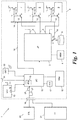
- a data processing device 1 comprises a housing 2 (only shown schematically here) for the secure and protected accommodation of the components arranged therein.
- the data processing device 1 is, for example, a desktop, laptop, notebook, handheld or tablet computer or a smartphone.
- the housing 2 is highly stable and preferably secured in such a way that access to the components of the data processing device 1 inside the housing is as difficult as possible.
- the housing 2 can be splash-proof or waterproof, protected against irradiation and radiation, protected against heat, shock and impact, bulletproof and explosion-proof, etc.
- a processor 3 with a volatile program memory 4 connected to it and one or more hardware components 6 - 9 connected to the processor 3 via data lines 5 are arranged in the housing 2 - on one or more circuit boards with corresponding connecting lines. All components of the data processing device 1 are supplied with power from a housing-internal or housing-external power supply 10, as are the hardware components 6 - 9 via exemplary power supply lines 11.
- a controllable switch 12 is interposed in each of the data lines 5 of the hardware components 6-9.
- a controllable switch 13 is interposed in each of the power supply lines 11 of the hardware components 6-9.
- the switches 12, 13 are controlled by a microcontroller 15 in the housing 2 via control lines 14.
- the microcontroller 15 has an interface 16 from the housing 2 to the outside.
- the interface 16 may be both wired and wireless, for example it is a USB interface, a short range radio interface according to an RFID, WLAN, NFC or Bluetooth ® standard, or the like.
- the interface 16 could, however, also be formed by a hardware component 6-9 designed as an interface module, if desired.
- a persistent key memory 17 and a trusted platform module 18, the function of which will be explained in more detail later, are connected to the microcontroller 15.
- the key memory 17 could also be located directly in the microcontroller 15, as could the trusted platform module 18 or, viewed conversely, the microcontroller 15 could be formed by a processor element in the trusted platform module 18.
- the microcontroller 15 is programmed with firmware 19 that is stored in a persistent memory area inside the microcontroller 15, in the key memory 17 and / or in the Trusted platform module 18 is stored and the microcontroller 15 can perform the functions described below.
- a memory module 20 is detachably connected to the interface 16.
- an administrator terminal 21 can also be connected via the interface 16 for configuring, in particular, the microcontroller 15, the key memory 17 and / or the trusted platform module 18.
- the memory module 20 is, for example, a “pure” memory such as a semiconductor memory card, for example a USB memory stick, an SD memory card, an RFID or NFC tag or the like. Or it is also equipped with its own computing power, ie has in addition to its memory also has its own processor, such as a SIM card, a cryptographic dongle, a smartphone, a PDA (Personal Digital Assistant), a "wearable” such as a digital bracelet, a smart watch or generally any type of digital device, that can be worn on or even in the body of the user.
- a “pure” memory such as a semiconductor memory card, for example a USB memory stick, an SD memory card, an RFID or NFC tag or the like.
- it is also equipped with its own computing power, ie has in addition to its memory also has its own processor, such as a SIM card, a cryptographic dongle, a smartphone, a PDA (Personal Digital Assistant), a "wearable” such as a digital bracelet, a smart watch
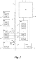
- Fig. 2 shows the storage of various key pairs 22-24 in the components described above.
- Each key pair 22-24 consists of a private key priv and a public key pub.
- data of a communication subscriber A which he has signed with his private key priv A
- the most varied of memory modules 20 from a set of memory modules SM 1 , SM 2 ,..., Generally SM 1 can be authenticated with respect to the data processing device 2.
- the public key pub A, i of the memory module SM i is stored in the key memory 17 of the microcontroller 15 - for example during the production, initialization and / or distribution of the data processing device 1 to a user in the field.
- the memory module SM i itself contains the associated private key priv A, i ; the public key pub A , i and the private key priv A, i form a first key pair 22.
- the microcontroller 15 is thus able to authenticate the memory module 20 or SM i when it is connected, ie to check its authorization for the operation of the data processing device 1.
- the microcontroller 19 receives via the interface 16 a signature 25 of the memory module SM i generated by the memory module SM i with the private key pri-v A, i and verifies it with the public key pub A, i stored in the key memory 17.
- the microcontroller 15 switches the switches 12, 13 on; if the verification fails, it switches the switches 12, 13 off.
- a hardware component 6-9 does not necessarily have to have both switches 12, 13. For example, only its data line 5 could be switched via a switch 12, or only its power supply line 11 via a switch 13. If a hardware component 6-9 has both a data switch 12 and a power switch 13, as a rule - if not mandatory - both switches 12, 13 switched on or off together.
- a specific subgroup of all available hardware components 6-9 can be assigned to a specific memory module SM i , which is switched on by the microcontroller 15 in the case of verification.
- the hardware components 6-9 to be switched on can then be selected by corresponding identification of that public key pub A , i whose verification was successful and to which, for example, a list of hardware components 6-9 is assigned in the key memory 17.
- the memory module SM i could also send a list of the hardware components 6-9 to be switched on with the signature 25.
- the microcontroller 15 continuously checks the presence of the connected memory module 20 or the interface 16 detects a removal or failure of the memory module 20 in order to immediately switch off the hardware components 6-9 that were previously switched on.
- the microcontroller 15 can then load the program or the data 27 from the memory module 20 via the interface 16 and feed it to the processor 3, for example for storage in the program memory 4 or a hardware component 6-9, e.g. the mass memory 6.
- the program or the data 27 When the program or the data 27 is transmitted via the interface 16, it can be encrypted with the aid of a second public / private key pair 23 composed of a public key pub B, j and a private key priv B, j.
- the private key priv B, j of the second key pair 23 is stored in the key memory 17 of the microcontroller 15 and the public key pub B. j of the second pair of keys 23 in the memory module 20.
- the memory module 20 can now encrypt the program or the data 27 with the public key pub B, j of the data processing device 1 and send it via the interface 16, and the microcontroller 15 can transmit the encrypted program or data. decrypt the data 27 encrypted in this way with the private key priv B, j stored in the key memory 17.
- a plurality of different second key pairs can be used 23, ie in the key store 17 corresponding to a plurality of private keys priv B, i, priv B, 2, ..., priv B are stored j to different, with the respective associated public key pub B, j , pub B, j ..., pub B, j to decrypt encrypted programs or data 27.
- the set of public keys stored in the key memory 17 can be pub A, i , pub A, 2 , ..., pub A, i , each of which is one connectable memory module SM 1 , SM 2 , ..., SM i are assigned, modified, for example, to authorize the data processing device 1 for use with different memory modules 20 each with different programs 27 for different missions.
- the public key pub M of a master key pair 24 is optionally stored in a specially protected part of the device 1, in particular the trusted platform module 18.
- the associated private key priv M of the master key pair 24 is stored in an administrator terminal 21.
- the microcontroller 15 can receive a signature 28 of the administrator terminal 21 generated with the private key priv M of the administrator terminal 21 and this using the public key pub M of the master stored in the trusted platform module 18 Verify key pair 24. In the case of verification, the microcontroller 15 allows a list 29 with one or more new or updated public keys pub A , i to be received from the administrator terminal 21 and stored in the key memory 17 instead of or in addition to the public keys pub A already present there, i .
- the data processing device 1 can thus be configured with the aid of the administrator terminal 21 for use with the most diverse, even only temporarily valid memory modules 20.
- the private key (s) priv B, 1 , priv B, 2 ,..., Priv B, j stored in the key memory 17 can also be modified in the same way.
- the power supply 10 can be provided with a power failure detector 30, which activates the microcontroller 15 to delete the key memory 17 in the event of a failure or disruption of the power supply 10.
- a power failure detector 30 which activates the microcontroller 15 to delete the key memory 17 in the event of a failure or disruption of the power supply 10.
- the microcontroller 15 can also use the public key pub M of the master key pair 24 in the trusted platform module 18 delete, whereby the data processing device 1 can no longer be configured using the administrator terminal 21 via the interface 16 and is thus made unusable.
- part or the entire program in the microcontroller 15 could also be deleted.
- a similar “emergency deletion function” for the key memory 17 and / or the trusted platform module 18 can also be brought about with the aid of a switch 31 which can be actuated by the user and which is accessible from the outside of the housing 2.
- the microcontroller 15 can be programmed so that when the manipulation sensor 32 responds, it deletes the key memory 17 and / or the trusted platform module 18 in order to prevent further use of a manipulated data processing device 1 or to make it unusable at all.
Landscapes
- Engineering & Computer Science (AREA)
- Theoretical Computer Science (AREA)
- Computer Hardware Design (AREA)
- Computer Security & Cryptography (AREA)
- General Physics & Mathematics (AREA)
- Physics & Mathematics (AREA)
- General Engineering & Computer Science (AREA)
- Software Systems (AREA)
- Signal Processing (AREA)
- Computer Networks & Wireless Communication (AREA)
- Health & Medical Sciences (AREA)
- Bioethics (AREA)
- General Health & Medical Sciences (AREA)
- Storage Device Security (AREA)
- Electrophonic Musical Instruments (AREA)
- Devices For Checking Fares Or Tickets At Control Points (AREA)
Description
- Die vorliegende Erfindung betrifft ein Datenverarbeitungsgerät, mit einem Gehäuse, in dem ein Prozessor, ein an den Prozessor angeschlossener Programmspeicher und zumindest eine an den Prozessor über eine Datenleitung angeschlossene und über eine Stromversorgungsleitung stromversorgte Hardwarekomponente angeordnet sind.
- Die
US 2015/0186684 A1 beschreibt eine Stromversorgung für ein Datenverarbeitungsgerät. Die Stromversorgung hat einen Empfänger zum Anschließen eines elektronischen Tags mit einem Autorisierungscode. Der Empfänger vergleicht den vom Tag empfangenen Autorisierungscode mit einem vorgegebenen Code und schaltet im Verifizierungsfall die Stromversorgung über einen Transistorschalter an das Gerät an. - Für sicherheitskritische Anwendungen, insbesondere im behördlichen und industriellen Bereich, ist der Schutz von Datenverarbeitungsgeräten gegenüber Manipulationen und Hacker-Angriffen von strategischer Bedeutung. Enormer Aufwand wird getrieben, um Geräte mittels physischer Zugangsbarrieren und Software-Firewalls entsprechend abzusichern. Besonders der Schutz von mobilen Datenverarbeitungsgeräten im Feld mit Standardbetriebssystemen und -applikationen ist aufgrund des leichten physischen Zugangs zu diesen Geräten, deren meist offener Schnittstellen und der weiten Verbreitung von Schadsoftware für solche Geräte ein großes Problem.
- Die Erfindung setzt sich zum Ziel, ein Datenverarbeitungsgerät der eingangs genannten Art mit verbesserter Sicherheit zu schaffen, insbesondere für den mobilen Einsatz im Feld.
- Dieses Ziel wird mit einem Datenverarbeitungsgerät der einleitend genannten Art erreicht, welches sich auszeichnet durch
- einen im Gehäuse angeordneten Mikrokontroller mit einer Schnittstelle und einem persistenten Schlüsselspeicher, in dem der Public Key eines ersten Public/Private-Key-Schlüsselpaares hinterlegt ist,
- wobei in die Datenleitung der genannten zumindest einen Hardwarekomponente ein vom Mikrokontroller gesteuerter Schalter zwischengeschaltet ist, und
- wobei der Mikrokontroller dafür ausgebildet ist, eine mit dem Private Key des ersten Schlüsselpaares erzeugte Signatur eines an die Schnittstelle lösbar angeschlossenen Speichermoduls über die Schnittstelle zu empfangen, anhand des Public Key des ersten Schlüsselpaares zu verifizieren und im Verifizierungsfall den Schalter einzuschalten.
- Die Erfindung schafft ein völlig neuartiges Sicherheitskonzept für ein Datenverarbeitungsgerät. Das Sicherheitskonzept besteht aus einer Kombination von geräteinternen Schaltern für die An- und Abschaltung von Hardwarekomponenten und einer Softwareauthentifizierung eines extern anschließbaren Speichermoduls, welches gleichsam als "Schlüssel" für die ordnungsgemäße Inbetriebnahme des Geräts dient. Dazu ist ein eigener Mikrokontroller im Gehäuse angeordnet, der als "Security Gateway" für die Inbetriebnahme der Hardwarekomponenten wirkt, indem er die Authentifizierung des externen Speichermoduls abwickelt und davon abhängig die Hardwareschalter bedient. Da ein Betrieb des Datenverarbeitungsgeräts ohne ein entsprechend authentifiziertes Speichermodul nicht möglich ist, ist die Gefahr von Manipulationen des Datenverarbeitungsgeräts reduziert.
- Unter dem Begriff "Speichermodul" wird in der vorliegenden Offenbarung jede Art von Hardwarekomponente verstanden, welche befähigt ist, die genannte Signatur über die Schnittstelle an das Datenverarbeitungsgerät zu senden. Das Speichermodul kann dabei entweder die genannte Signatur bereits vorberechnet enthalten oder nur den genannten Private Key, um daraus bei Bedarf die Signatur zu erzeugen. Beispielsweise ist das Speichermodul - insbesondere im ersten Fall - ein bloßer Speicher wie eine Halbleiterspeicherkarte, ein Speicherstick oder -chip, ein RFID- oder NFC-Tag od.dgl., oder - insbesondere im zweiten Fall - auch mit eigener Rechenleistung ausgestattet, z.B. eine SIM-Karte, ein kryptographischer Dongle, ein Smartphone od.dgl.
- Die solcherart geschaltete(n) Hardwarekomponente(n) des Datenverarbeitungsgeräts können beliebiger Art sein. Beispiele sind ein drahtgebundenes oder drahtloses Schnittstellenmodul, z.B. eine USB-Schnittstelle, eine Speicherkartenschnittstelle, eine Funkschnittstelle wie ein WiFi®-, Bluetooth®- oder Mobilfunknetz-Modul, eine Ein- und/oder Ausgabeeinheit wie eine Tastatur, ein Bildschirm oder Touchscreen, eine Kamera oder auch jede andere Art von Umweltsensor. Eine der geschalteten Hardwarekomponenten kann insbesondere auch ein persistenter, d.h. nicht-flüchtiger, Massenspeicher sein, z.B. eine Magnetfestplatte oder eine optische Platte, im Gegensatz zum Programmspeicher des Prozessors, der bevorzugt ein flüchtiger Speicher ist. Ohne ein vom Mikrokontroller authentifiziertes Speichermodul verfügt das Datenverarbeitungsgerät somit über keinen Massenspeicher mit darin gespeicherten Betriebssystem- und Applikationsprogrammen, d.h. ist gleichsam "leer". Erst durch Anschließen des richtigen Speichermoduls werden die entsprechenden Hardwarekomponenten, z.B. der persistente Massenspeicher mit den Programmen und die notwendigen Schnittstellen, Kameras, Sensoren usw., verfügbar und das Gerat einsatzfähig. Je nach angeschlossenem Speichermodul können dabei auch verschiedene Hardwarekomponenten freigeschaltet werden.
- Zusätzlich zu dem die Datenleitung der jeweiligen Hardwarekomponente schaltenden Schalter kann in die Stromversorgungsleitung der jeweiligen Hardwarekomponente ein vom Mikrokontroller gesteuerter weiterer Schalter zwischengeschaltet und der Mikrokontroller dafür ausgebildet sein, im Verifizierungsfall auch diesen weiteren Schalter einzuschalten, um die Sicherheit zu erhöhen.
- In einer besonders bevorzugten Ausführungsform der Erfindung kann der Mikrokontroller dafür ausgebildet sein, im Verifizierungsfall ein Programm und/oder Daten aus dem Speichermodul über die Schnittstelle zu laden. Das Datenverarbeitungsgerät kann so beispielsweise ohne jeglichen persistenten Massenspeicher distribuiert werden. Die für den Betrieb erforderlichen Systemprogramme, Applikationen und Daten können auf dem zertifizierten Speichermodul an die Benutzer verteilt werden; erst bei Anschließen des jeweiligen gegenüber dem Datenverarbeitungsgerät authentifizierten Speichermoduls wird das Datenverarbeitungsgerät mit den Programmen und Daten geladen und kann in Betrieb genommen werden.
- Bevorzugt wird dabei in dem Schlüsselspeicher der Private Key eines zweiten Public/Private-Key-Schlüsselpaares hinterlegt und der Mikrokontroller ist dafür ausgebildet, ein mit dem Public Key des zweiten Schlüsselpaares verschlüsseltes Programm oder derart verschlüsselte Daten über die Schnittstelle zu laden, mit dem Private Key des zweiten Schlüsselpaares zu entschlüsseln und dem Prozessor zwecks Speicherung im Programmspeicher oder der Hardwarekomponente zuzuführen. Die Datenübertragung des Programms vom Speichermodul in das Datenverarbeitungsgerät erfolgt so verschlüsselt und immun gegenüber Abhörangriffen an der Schnittstelle.
- Der Schlüsselspeicher, in dem der Public Key des externen Speichermoduls hinterlegt ist, kann beispielsweise direkt im Mikrokontroller oder einem daran angeschlossenen Speicher beheimatet sein. Alternativ kann der Schlüsselspeicher auch in einem Trusted-Platform-Modul (TPM) liegen, das an den Mikrokontroller angeschlossen ist. Ein solches TPM kann in einer weiteren vorteilhaften Ausgestaltung der Erfindung dazu verwendet werden, darin den Public Key eines Public/Private-Key-Master-Schlüsselpaares zu hinterlegen, wobei dann der Mikrokontroller dafür ausgebildet ist, einen mit dem Private Key des Master-Schlüsselpaares signierten Public Key über die Schnittstelle zu empfangen, dessen Signatur anhand des Public Key des Master-Schlüsselpaares zu verifizieren und im Verifizierungsfall den empfangenen Public Key im Schlüsselspeicher zu hinterlegen. Ein Administrator, der über den Private Key des Master-Schlüsselpaares verfügt, kann so beispielsweise mit einem an die Schnittstelle angeschlossenen Administratorterminal anwendungs- bzw. missionsspezifische Public Keys hinterlegen und das Datenverarbeitungsgerät damit für Nutzer mit entsprechend anwendungs- bzw. missionsspezifisch authorisierten Speichermodulen vorbereiten.
- Die Schnittstelle, welche zum Anschluss des externen Speichermoduls bzw. des optionalen Administratorterminals dient, kann sowohl drahtgebunden als auch drahtlos sein, z.B. eine Kurzreichweiten-Funkschnittstelle nach einem RFID (radio frequency identification), WLAN (wireless local area network), NFC (near field communication) oder Bluetooth®-Standard. Bevorzugt ist die Schnittstelle drahtgebunden und insbesondere bevorzugt eine USB-Schnittstelle, um physische Zuordnungssicherheit zu gewährleisten.
- Gemäß einem weiteren bevorzugten Merkmal der Erfindung ist das Gehäuse mit einem an den Mikrokontroller angeschlossenen Manipulationssensor ausgestattet und der Mikrokontroller dafür ausgebildet, bei Ansprechen des Manipulationssensors den bzw. die Schalter auszuschalten. Ein solcher Manipulationssensor kann beispielsweise die Integrität des Gehäuses überwachen und auf ein Öffnen oder Beschädigen des Gehäuses ansprechen, um dann eine oder mehrere Hardwarekomponenten zu deaktivieren. Dabei kann der Mikrokontroller bei Ansprechen des Manipulationssensors bevorzugt auch den Schlüsselspeicher löschen, um jedwede weitere Inbetriebnahme selbst bei neuerlichem Anschließen des Speichermoduls zu verhindern.
- Alternativ oder zusätzlich kann das Datenverarbeitungsgerät mit einem an den Mikrokontroller angeschlossenen Stromausfalldetektor ausgestattet und der Mikrokontroller dafür ausgebildet sein, bei Ansprechen des Stromausfalldetektors den Schlüsselspeicher zu löschen. Der weitere Betrieb des Geräts kann so auch bei einer Manipulation an der Stromversorgung unterbunden werden. In der Ausführungsform mit Trusted-Platform-Modul kann der Mikrokontroller ferner überdies bei Ansprechen des Stromausfalldetektors den Public Key des Master-Schlüsselpaares im Trusted-Platform-Modul löschen. Ohne Master-Public-Key können keine speichermodulspezifischen Public Keys mehr hinterlegt werden, sodass das Gerät nach der Detektion eines Stromausfalls dauerhaft unbrauchbar gemacht ist.
- Die Erfindung wird nachstehend anhand von in den beigeschlossenen Zeichnungen dargestellten Ausführungsbeispielen näher erläutert. In den Zeichnungen zeigt:
-
Fig. 1 ein Blockschaltbild des Datenverarbeitungsgeräts der Erfindung in Verbindung mit einem Speichermodul und einem Administratorterminal; und -
Fig. 2 einen Detailausschnitt des Schaltbilds vonFig. 1 . - Gemäß
Fig. 1 umfasst ein Datenverarbeitungsgerät 1 ein (hier nur schematisch dargestelltes) Gehäuse 2 zur sicheren und geschützten Aufnahme der darin angeordneten Komponenten. Das Datenverarbeitungsgerät 1 ist beispielsweise ein Desktop-, Laptop-, Notebook-, Handheld- oder Tablet-Computer oder ein Smartphone. Das Gehäuse 2 ist hochstabil und bevorzugt so abgesichert, dass ein Zugang zu den Komponenten des Datenverarbeitungsgeräts 1 im Inneren des Gehäuses größtmöglich erschwert ist. Das Gehäuse 2 kann spritzwassergeschützt oder wasserdicht sein, ein- und abstrahlungsgeschützt, hitze-, stoß- und aufprallgeschützt, schuss- und explosionssicher usw. - In dem Gehäuse 2 sind - auf einer oder mehreren Platinen mit entsprechenden Verbindungsleitungen - ein Prozessor 3 mit einem daran angeschlossenen flüchtigen Programmspeicher 4 sowie eine oder mehrere an den Prozessor 3 über Datenleitungen 5 angeschlossene Hardwarekomponenten 6 - 9 angeordnet. Alle Komponenten des Datenverarbeitungsgeräts 1 werden von einer gehäuseinternen oder gehäuseexternen Stromversorgung 10 stromversorgt, so auch die Hardwarekomponenten 6 - 9 über beispielhafte Stromversorgungsleitungen 11.
- Jede der (hier beispielhaft: vier) Hardwarekomponenten 6 - 9 kann insbesondere sein:
- ein persistenter, d.h. nicht-flüchtiger, Massenspeicher, z.B. eine magnetische Festplatte, eine optische Speicherplatte, ein Flash-Speicher, ein ROM, PROM, EPROM, EEPROM usw.;
- ein kabelgebundenes Schnittstellenmodul, z.B. eine USB-, Firewire®- oder HDMI-Schnittstelle oder eine SpeicherkartenSchnittstelle, z.B. für SD-Speicherkarten;
- ein Funkschnittstellenmodul, z.B. ein WiFi®-, Bluetooth®-, NFC- oder RFID-Modul oder ein Mobilfunknetzmodul nach einem 2G-, 3G-, 4G- oder 5G-Standard wie GSM, UMTS, LTE, 5G od.dgl.;
- eine Kamera oder ein beliebiger anderer Umweltsensor, z.B. ein Temperatur-, Schall- oder Lichtsensor für Temperatur, Licht und Schall innerhalb und/oder außerhalb des Gehäuses 2;
- ein chemischer Sensor, Luftgütesensor, Sensor zur Erkennung von Radioaktivität, Entfernungsmesser, Multimeter, Datenlogger od.dgl;
- eine Ein- und/oder Ausgabeeinheit wie eine Tastatur, ein Bildschirm, ein Touchscreen od.dgl.;
- ein Satellitennavigationsempfänger, z.B. ein GPS-, Galileo- oder Glonass-Empfänger;
- ein Lage- bzw. Beschleunigungsmessgerät oder eine IMU (Inertial Measurement Unit);
- ein Audiomodul für Ton- oder Sprachein- und -ausgabe.
- In die Datenleitungen 5 der Hardwarekomponenten 6 - 9 ist jeweils ein steuerbarer Schalter 12 zwischengeschaltet. Ebenso ist in jede der Stromversorgungsleitungen 11 der Hardwarekomponenten 6 - 9 jeweils ein steuerbarer Schalter 13 zwischengeschaltet. Die Schalter 12, 13 sind über Steuerleitungen 14 von einem Mikrokontroller 15 im Gehäuse 2 gesteuert.
- Der Mikrokontroller 15 hat eine Schnittstelle 16 aus dem Gehäuse 2 nach außen. Die Schnittstelle 16 kann sowohl drahtgebunden als auch drahtlos sein, beispielsweise ist sie eine USB-Schnittstelle, eine Kurzreichweiten-Funkschnittstelle nach einem RFID-, WLAN-, NFC- oder Bluetooth®-Standard, od.dgl. Die Schnittstelle 16 könnte jedoch auch durch eine als Schnittstellenmodul ausgeführte Hardwarekomponente 6 - 9 gebildet sein, falls gewünscht.
- An den Mikrokontroller 15 sind ein persistenter Schlüsselspeicher 17 und ein Trusted-Platform-Modul 18 angeschlossen, deren Funktion später noch ausführlicher erläutert wird. Der Schlüsselspeicher 17 könnte auch direkt im Mikrokontroller 15 beheimatet sein, ebenso das Trusted-Platform-Modul 18, bzw. könnte umgekehrt betrachtet der Mikrokontroller 15 durch ein Prozessorelement im Trusted-Platform-Modul 18 gebildet sein.
- Der Mikrokontroller 15 ist mit einer Firmware 19 programmiert, die in einem persistenten Speicherbereich im Inneren des Mikrokontrollers 15, im Schlüsselspeicher 17 und/oder im Trusted-Platform-Modul 18 gespeichert ist und den Mikrokontroller 15 die im Weiteren beschriebenen Funktionen ausführen lässt.
- An die Schnittstelle 16 ist ein Speichermodul 20 lösbar angeschlossen. Über die Schnittstelle 16 kann alternativ oder zusätzlich auch ein Administratorterminal 21 zur Konfiguration insbesondere des Mikrokontrollers 15, des Schlüsselspeichers 17 und/oder des Trusted-Platform-Moduls 18 angeschlossen werden.
- Das Speichermodul 20 ist beispielsweise ein "reiner" Speicher wie eine Halbleiterspeicherkarte, z.B. ein USB-Speicherstick, eine SD-Speicherkarte, ein RFID- oder NFC-Tag od.dgl., oder es ist auch mit eigener Rechenleistung ausgestattet, d.h. hat zusätzlich zu seinem Speicher auch einen eigenen Prozessor, wie beispielsweise eine SIM-Karte, ein kryptographischer Dongle, ein Smartphone, ein PDA (Personal Digital Assistant), ein "Wearable" wie ein digitales Armband, eine Smart-Watch oder allgemein jede Art von digitalem Device, das am oder sogar im Körper des Benutzers getragen werden kann.
-
Fig. 2 zeigt die Einspeicherung verschiedenster Schlüsselpaare 22 - 24 in den oben beschriebenen Komponenten. Jedes Schlüsselpaar 22 - 24 besteht aus einem privaten Schlüssel ("Private Key") priv und einem öffentlichen Schlüssel ("Public Key") pub. Wie in der Technik bekannt, können Daten eines Kommunikationsteilnehmers A, die dieser mit seinem Private Key privA signiert hat, von einem anderen Teilnehmer B durch Nachrechnen der Signatur mit Hilfe des Public Key pubA des Teilnehmers A authentifiziert, d.h. auf tatsächliche Signierung mit dem Private Key privA, überprüft werden; und wenn der Teilnehmer A Daten mit dem Public Key pubB des Teilnehmers B verschlüsselt hat, können diese verschlüsselten Daten vom Teilnehmer B mit dessen Private Key privB entschlüsselt werden. - Mit einem solchen Public/Private-Key-Verschlüsselungsverfahren können verschiedenste Speichermodule 20 aus einem Satz von Speichermodulen SM1, SM2, ..., allgemein SM1, gegenüber dem Datenverarbeitungsgerät 2 authentifiziert werden. Zunächst, wird - beispielsweise bei der Herstellung, Initialisierung und/oder Verteilung des Datenverarbeitungsgeräts 1 an einen Benutzer im Feld - der Public Key pubA,i des Speichermoduls SMi im Schlüsselspeicher 17 des Mikrokontroller 15 hinterlegt. Das Speichermodul SMi selbst enthält den zugehörigen Private Key privA,i; der Public Key pubA,i und der Private Key privA,i bilden ein erstes Schlüsselpaar 22.
- Der Mikrokontroller 15 ist damit in der Lage, bei Anschließen des Speichermoduls 20 bzw. SMi dieses zu authentifizieren, d.h. seine Berechtigung für den Betrieb des Datenverarbeitungsgeräts 1 zu überprüfen. Dazu empfängt der Mikrokontroller 19 über die Schnittstelle 16 eine mit dem Private Key pri-vA,i vom Speichermodul SMi erzeugte Signatur 25 des Speichermoduls SMi und verifiziert sie mit dem im Schlüsselspeicher 17 gespeicherten Public Key pubA,i. Im Verifizierungsfall, d.h. bei erfolgreicher Verifizierung, schaltet der Mikrokontroller 15 die Schalter 12, 13 ein, schlägt die Verifizierung fehl, schaltet er die Schalter 12, 13 aus.
- Es versteht sich, dass eine Hardwarekomponente 6 - 9 nicht notwendigerweise über beide Schalter 12, 13 verfügen muss. Beispielsweise könnte nur ihre Datenleitung 5 über einen Schalter 12 geschaltet sein, oder nur ihre Stromversorgungsleitung 11 über einen Schalter 13. Wenn eine Hardwarekomponente 6 - 9 sowohl über einen Datenschalter 12 als auch über einen Stromschalter 13 verfügt, werden in der Regel - wenn auch nicht zwingend - beide Schalter 12, 13 gemeinsam ein- oder ausgeschaltet.
- Einem bestimmten Speichermodul SMi kann eine bestimmte Untergruppe aller verfügbaren Hardwarekomponenten 6 - 9 zugeordnet sein, die vom Mikrokontroller 15 im Verifizierungsfall eingeschaltet wird. Die Auswahl der jeweils einzuschaltenden Hardwarekomponenten 6 - 9 kann dann durch entsprechende Identifikation jenes Public Key pubA,i erfolgen, dessen Verifizierung erfolgreich war, und dem z.B. im Schlüsselspeicher 17 eine Liste von Hardwarekomponenten 6 - 9 zugeordnet ist. Alternativ könnte das Speichermodul SMi mit der Signatur 25 auch eine Liste der einzuschaltenden Hardwarekomponenten 6 - 9 senden.
- Optional kontrolliert der Mikrokontroller 15 laufend das Vorhandensein des angeschlossenen Speichermoduls 20 bzw. detektiert die Schnittstelle 16 ein Abziehen oder einen Ausfall des Speichermoduls 20, um die zuvor eingeschalteten Hardwarekomponenten 6 - 9 umgehend auszuschalten.
- In einem oder mehreren der Speichermodule SMi können optional Programme oder Daten 27, beispielsweise das Betriebssystem des Datenverarbeitungsgeräts 1, Betriebsdaten und/oder Applikationen, gespeichert sein. Der Mikrokontroller 15 kann dann im Verifizierungsfall das Programm bzw. die Daten 27 aus dem Speichermodul 20 über die Schnittstelle 16 laden und dem Prozessor 3 zuführen, beispielsweise zwecks Speicherung im Programmspeicher 4 oder einer Hardwarekomponente 6 - 9, z.B. dem Massenspeicher 6.
- Bei Übertragung des Programms bzw. der Daten 27 über die Schnittstelle 16 kann dieses mithilfe eines zweiten Public/Private-Key-Schlüsselpaares 23 aus einem Public Key pubB,j und einem Private Key privB,j verschlüsselt werden. Dazu ist der Private Key privB,j des zweiten Schlüsselpaares 23 im Schlüsselspeicher 17 des Mikrokontrollers 15 hinterlegt und der Public Key pubB.j des zweiten Schlüsselpaares 23 im Speichermodul 20. Das Speichermodul 20 kann nun das Programm bzw. die Daten 27 mit dem Public Key pubB,j des Datenverarbeitungsgeräts 1 verschlüsseln und über die Schnittstelle 16 senden, und der Mikrokontroller 15 kann das verschlüsselte Programm bzw. die derart verschlüsselten Daten 27 mit dem im Schlüsselspeicher 17 gespeicherten Private Key privB,j entschlüsseln.
- Erforderlichenfalls können auch mehrere verschiedene zweite Schlüsselpaare 23 verwendet werden, d.h. im Schlüsselspeicher 17 entsprechend mehrere Private Keys privB,i, privB,2, ..., privB,j gespeichert werden, um unterschiedliche, mit dem jeweils zugehörigen Public Key pubB,j, pubB,j ..., pubB,j verschlüsselte Programme bzw. Daten 27 zu entschlüsseln.
- Optional kann der Satz von im Schlüsselspeicher 17 gespeicherten Public Keys pubA,i, pubA,2, ..., pubA,i, welche jeweils einem anschließbaren Speichermodul SM1, SM2, ..., SMi zugeordnet sind, modifiziert werden, beispielsweise um das Datenverarbeitungsgerät 1 zur Verwendung mit unterschiedlichen Speichermodulen 20 mit jeweils unterschiedlichen Programmen 27 für unterschiedliche Missionen zu authorisieren. Zu diesem Zweck ist optional in einem besonders geschützten Teil des Geräts 1, insbesondere dem Trusted-Platform-Modul 18, der Public Key pubM eines Master-Schlüsselpaares 24 hinterlegt. Der zugehörige Private Key privM des Master-Schlüsselpaares 24 ist in einem Administratorterminal 21 gespeichert. Wenn das Administratorterminal 21 an die Schnittstelle 16 angeschlossen wird, kann der Mikrokontroller 15 eine mit dem Private Key privM des Administratorterminals 21 erzeugte Signatur 28 des Administratorterminals 21 empfangen und diese mithilfe des im Trusted-Platform-Modul 18 gespeicherten Public Key pubM des Master-Schlüsselpaares 24 verifizieren. Im Verifizierungsfall gestattet der Mikrokontroller 15, dass eine Liste 29 mit einem oder mehreren neuen bzw. aktualisierten Public Keys pubA,i vom Administratorterminal 21 her empfangen und im Schlüsselspeicher 17 gespeichert wird, anstelle oder zusätzlich zu den bereits dort vorhandenen Public Keys pubA,i. Das Datenverarbeitungsgerät 1 kann so mithilfe des Administratorterminals 21 zur Verwendung mit verschiedensten, auch nur temporär gültigen Speichermodulen 20 konfiguriert werden.
- Auf dieselbe Weise können im übrigen auch der oder die im Schlüsselspeicher 17 gespeicherten Private Key(s) privB,1, privB,2, ..., privB,j modifiziert werden.
- Als weitere Sicherheitsmaßnahme gegenüber Betriebsstörungen oder Manipulationen des Datenverarbeitungsgeräts 1 kann die Stromversorgung 10 mit einem Stromausfallsdetektor 30 versehen sein, welcher den Mikrokontroller 15 bei einem Ausfall oder einer Störung der Stromversorgung 10 dazu ansteuert, den Schlüsselspeicher 17 zu löschen. Dadurch gibt es keine im Schlüsselspeicher 17 mehr hinterlegten Public Keys pubA,i zur Authentifizierung von angeschlossenen Speichermodulen 20. Optional kann der Mikrokontroller 15 bei Ansprechen des Stromausfalldetektors 30 auch den Public Key pubM des Master-Schlüsselpaares 24 im Trusted-Platform-Modul 18 löschen, wodurch das Datenverarbeitungsgerät 1 nicht mehr mithilfe des Administratorterminals 21 über die Schnittstelle 16 konfigurierbar und damit unbrauchbar gemacht ist. Zusätzlich könnte auch ein Teil oder das gesamte Programm im Mikrokontroller 15 gelöscht werden.
- Eine gleichartige "Notlöschfunktion" für den Schlüsselspeicher 17 und/oder das Trusted-Platform-Modul 18 kann auch mithilfe eines vom Benutzer betätigbaren Schalters 31 bewirkt werden, der von der Außenseite des Gehäuses 2 her zugänglich ist.
- Als zusätzliche Sicherheitsmaßnahme kann das Gehäuse 2 mit einem Manipulationssensor 32 ausgestattet sein. Der Manipulationssensor 32 detektiert Manipulationen am bzw. im Gehäuse 2, z.B. ein Öffnen, Beschädigen, Erschüttern, Überhitzen, Unterkühlen, Bestrahlen oder Beschallen usw., und veranlasst dann den Mikrokontroller 15 dazu, die Schalter 12, 13 auszuschalten und/oder die vorgenannte Notlöschfunktion auszulösen. Ein solcher Manipulationssensor 32 kann beispielsweise sein:
- ein Schaltkontakt, der beim Öffnen des Gehäuses 2 schließt oder öffnet und dieses Ansprechen dem Mikrokontroller 15 signalisiert;
- ein Widerstandsmessgerät, welches den elektrischen Widerstand der Gehäusewandung des Gehäuses 2 überwacht, beispielsweise zwischen Elektroden, die über die Wandung des Gehäuses 2 verteilt sind, oder in einem Gitter aus leitfähiger Tinte, Drähten usw., um Sprünge oder Risse in Gehäuse 2 anhand von Widerstandsenderungen zu detektieren;
- ein Mikrophon für den Innenraum des Gehäuses 2, welches strukturelle Änderungen im Gehäuse 2 anhand einer Veränderung des Schallübertragungs- oder -reflexionsverhaltens des Gehäuseinneren detektiert;
- eine Festkörperschall-Überwachungseinrichtung, welche solche strukturelle Änderungen anhand des Schallübertragungs- oder -resonanzverhaltens der Festkörperstruktur des Gehäuses 2 und seiner darin montierten Komponenten für darin eingeleitete Schall- oder Ultraschallwellen detektiert;
- andere Arten von Licht- oder Schalldetektoren im oder am Gehäuse 2, die z.B. ein Öffnen des Gehäuses 2 aufgrund von Eindringen von Licht oder Schall in das Gehäuse 2 detektieren;
- Kameras, die in das Innere des Gehäuses oder nach außen gerichtet sind, um Manipulationen am oder im Gehäuse 2 zu detektieren; usw. usf.
- Der Mikrokontroller 15 kann dabei so programmiert sein, dass er bei einem Ansprechen des Manipulationssensors 32 den Schlüsselspeicher 17 und/oder das Trusted-Platform-Modul 18 löscht, um eine Weiterverwendung eines manipulierten Datenverarbeitungsgeräts 1 zu unterbinden bzw. dieses überhaupt unbrauchbar zu machen.
- Die Erfindung ist nicht auf die dargestellten Ausführungsformen beschränkt, sondern umfasst alle Varianten, Modifikationen und deren Kombinationen, die in den Rahmen der angeschlossenen Ansprüche fallen.
Claims (15)
- Datenverarbeitungsgerät, mit einem Gehäuse (2), in dem ein Prozessor (3), ein an den Prozessor (3) angeschlossener Programmspeicher (4) und zumindest eine an den Prozessor (3) über eine Datenleitung (5) angeschlossene und über eine Stromversorgungsleitung (11) stromversorgte Hardwarekomponente (6 - 9) angeordnet sind, gekennzeichnet durcheinen im Gehäuse (2) angeordneten Mikrokontroller (15) mit einer Schnittstelle (16) und einem persistenten Schlüsselspeicher (17), in dem der Public Key (pubA,i) eines ersten Public/Private-Key-Schlüsselpaares (22) hinterlegt ist,wobei in die Datenleitung (5) ein vom Mikrokontroller (15) gesteuerter Schalter (12) zwischengeschaltet ist, undwobei der Mikrokontroller (15) dafür ausgebildet ist, eine mit dem Private Key (privA,i) des ersten Schlüsselpaares (22) erzeugte Signatur (25) eines an die Schnittstelle (16) lösbar angeschlossenen Speichermoduls (20) über die Schnittstelle (16) zu empfangen, anhand des Public Key (pubA,i) des ersten Schlüsselpaares (22) zu verifizieren und im Verifizierungsfall den Schalter (12) einzuschalten.
- Datenverarbeitungsgerät nach Anspruch 1, dadurch gekennzeichnet, dass in die Stromversorgungsleitung (11) ein vom Mikrokontroller (15) gesteuerter weiterer Schalter (13) zwischengeschaltet ist, wobei der Mikrokontroller (15) ferner dafür ausgebildet ist, im Verifizierungsfall auch den weiteren Schalter (13) einzuschalten.
- Datenverarbeitungsgerät nach Anspruch 1 oder 2, dadurch gekennzeichnet, dass der Mikrokontroller (15) dafür ausgebildet ist, im Verifizierungsfall ein Programm (27) aus dem Speichermodul (20) über die Schnittstelle (16) zu laden.
- Datenverarbeitungsgerät nach Anspruch 3, dadurch gekennzeichnet, dass in dem Schlüsselspeicher (17) der Private Key (privB,j) eines zweiten Public/Private-Key-Schlüsselpaares (23) hinterlegt und der Mikrokontroller (15) dafür ausgebildet ist, ein mit dem Public Key (pubB,j) des zweiten Schlüsselpaares (23) verschlüsseltes Programm oder derart verschlüsselte Daten (27) über die Schnittstelle (16) zu laden, mit dem Private Key (privB,j) des zweiten Schlüsselpaares (23) zu entschlüsseln und dem Prozessor (3) zwecks Speicherung im Programmspeicher (4) oder der Hardwarekomponente (6 - 9) zuzuführen.
- Datenverarbeitungsgerät nach einem der Ansprüche 1 bis 4, dadurch gekennzeichnet, dass in einem Trusted-Platform-Modul (18) des Mikrokontrollers (15) der Public Key (pubM) eines Public/Private-Key-Master-Schlüsselpaares (24) hinterlegt ist,
wobei der Mikrokontroller (15) dafür ausgebildet ist, einen mit dem Private Key (privM) des Master-Schlüsselpaares (24) signierten Public Key (pubA,i) über die Schnittstelle (16) zu empfangen, dessen Signatur (25) anhand des Public Key (pubM) des Master-Schlüsselpaares (24) zu verifizieren und im Verifizierungsfall den empfangenen Public Key (pubA,i) im Schlüsselspeicher (17) zu hinterlegen. - Datenverarbeitungsgerät nach einem der Ansprüche 1 bis 5, dadurch gekennzeichnet, dass die bzw. zumindest eine der Hardwarekomponente/n (6 - 9) ein persistenter Massenspeicher ist.
- Datenverarbeitungsgerät nach einem der Ansprüche 1 bis 5, dadurch gekennzeichnet, dass die bzw. zumindest eine der Hardwarekomponente/n (6 - 9) ein Funkschnittstellenmodul ist.
- Datenverarbeitungsgerät nach einem der Ansprüche 1 bis 5, dadurch gekennzeichnet, dass die bzw. zumindest eine der Hardwarekomponente/n (6 - 9) eine Kamera oder ein Umweltsensor ist.
- Datenverarbeitungsgerät nach einem der Ansprüche 1 bis 8, dadurch gekennzeichnet, dass die Schnittstelle eine drahtgebundene Schnittstelle (16) ist.
- Datenverarbeitungsgerät nach Anspruch 9, dadurch gekennzeichnet, dass die Schnittstelle eine USB-Schnittstelle ist.
- Datenverarbeitungsgerät nach einem der Ansprüche 1 bis 10, dadurch gekennzeichnet, dass das Gehäuse (2) mit einem an den Mikrokontroller (15) angeschlossenen Manipulationssensor (32) ausgestattet und der Mikrokontroller (15) dafür ausgebildet ist, bei Ansprechen des Manipulationssensors (32) den Schalter (12) auszuschalten.
- Datenverarbeitungsgerät nach einem der Ansprüche 2 bis 11, dadurch gekennzeichnet, dass das Gehäuse (2) mit einem an den Mikrokontroller (15) angeschlossenen Manipulationssensor (32) ausgestattet und der Mikrokontroller (15) dafür ausgebildet ist, bei Ansprechen des Manipulationssensors (32) den weiteren Schalter (13) auszuschalten.
- Datenverarbeitungsgerät nach Anspruch 11 oder 12, dadurch gekennzeichnet, dass der Mikrokontroller (15) ferner dafür ausgebildet ist, bei Ansprechen des Manipulationssensors (32) den Schlüsselspeicher (15) zu löschen.
- Datenverarbeitungsgerät nach einem der Ansprüche 1 bis 13, dadurch gekennzeichnet, dass es mit einem an den Mikrokontroller (15) angeschlossenen Stromausfalldetektor (30) ausgestattet und der Mikrokontroller (15) dafür ausgebildet ist, bei Ansprechen des Stromausfalldetektors (30) den Schlüsselspeicher (15) zu löschen.
- Datenverarbeitungsgerät nach den Ansprüchen 5 und 14, dadurch gekennzeichnet, dass der Mikrokontroller (15) ferner dafür ausgebildet ist, bei Ansprechen des Stromausfalldetektors (30) den Public Key (pubM) des Master-Schlüsselpaares (24) im Trusted-Platform-Modul (18) zu löschen.
Priority Applications (15)
| Application Number | Priority Date | Filing Date | Title |
|---|---|---|---|
| HRP20220047TT HRP20220047T1 (hr) | 2019-01-14 | 2019-01-14 | Uređaj za obradu podataka, zaštićen od manipuliranja |
| LTEP19151564.2T LT3680797T (lt) | 2019-01-14 | 2019-01-14 | Nuo klastojimo apsaugotas duomenų apdorojimo aparatas |
| ES19151564T ES2904799T3 (es) | 2019-01-14 | 2019-01-14 | Dispositivo de procesamiento de datos protegido contra manipulación |
| HUE19151564A HUE057629T2 (hu) | 2019-01-14 | 2019-01-14 | Manipuláció ellen védett adatfeldolgozó készülék |
| PT191515642T PT3680797T (pt) | 2019-01-14 | 2019-01-14 | Dispositivo de processamento de dados protegido contra manipulação |
| PL19151564T PL3680797T3 (pl) | 2019-01-14 | 2019-01-14 | Zabezpieczone przed manipulacją urządzenie do przetwarzania danych |
| DK19151564.2T DK3680797T3 (da) | 2019-01-14 | 2019-01-14 | Manipulations-beskyttet databehandlingsapparat |
| EP19151564.2A EP3680797B1 (de) | 2019-01-14 | 2019-01-14 | Manipulationsgeschütztes datenverarbeitungsgerät |
| JP2021540853A JP7482139B2 (ja) | 2019-01-14 | 2020-01-10 | 耐改ざんデータ処理装置 |
| KR1020217024675A KR102763803B1 (ko) | 2019-01-14 | 2020-01-10 | 변조방지 데이터 처리 디바이스 |
| CA3124026A CA3124026C (en) | 2019-01-14 | 2020-01-10 | Tamper-proof data processing device |
| US17/422,355 US11799649B2 (en) | 2019-01-14 | 2020-01-10 | Tamper-proof data processing device |
| PCT/EP2020/050504 WO2020148176A1 (de) | 2019-01-14 | 2020-01-10 | Manipulationsgeschütztes datenverarbeitungsgerät |
| IL284138A IL284138B2 (en) | 2019-01-14 | 2020-01-10 | Tamper-proof data processing device |
| CN202080009086.8A CN113330434B (zh) | 2019-01-14 | 2020-01-10 | 防篡改数据处理设备 |
Applications Claiming Priority (1)
| Application Number | Priority Date | Filing Date | Title |
|---|---|---|---|
| EP19151564.2A EP3680797B1 (de) | 2019-01-14 | 2019-01-14 | Manipulationsgeschütztes datenverarbeitungsgerät |
Publications (2)
| Publication Number | Publication Date |
|---|---|
| EP3680797A1 EP3680797A1 (de) | 2020-07-15 |
| EP3680797B1 true EP3680797B1 (de) | 2021-10-27 |
Family
ID=65030918
Family Applications (1)
| Application Number | Title | Priority Date | Filing Date |
|---|---|---|---|
| EP19151564.2A Active EP3680797B1 (de) | 2019-01-14 | 2019-01-14 | Manipulationsgeschütztes datenverarbeitungsgerät |
Country Status (14)
| Country | Link |
|---|---|
| US (1) | US11799649B2 (de) |
| EP (1) | EP3680797B1 (de) |
| JP (1) | JP7482139B2 (de) |
| KR (1) | KR102763803B1 (de) |
| CN (1) | CN113330434B (de) |
| DK (1) | DK3680797T3 (de) |
| ES (1) | ES2904799T3 (de) |
| HR (1) | HRP20220047T1 (de) |
| HU (1) | HUE057629T2 (de) |
| IL (1) | IL284138B2 (de) |
| LT (1) | LT3680797T (de) |
| PL (1) | PL3680797T3 (de) |
| PT (1) | PT3680797T (de) |
| WO (1) | WO2020148176A1 (de) |
Families Citing this family (3)
| Publication number | Priority date | Publication date | Assignee | Title |
|---|---|---|---|---|
| US10872161B2 (en) * | 2016-11-23 | 2020-12-22 | Entrust Corporation | Printer identity and security |
| AU2021337529A1 (en) * | 2020-09-05 | 2023-05-18 | Icu Medical, Inc. | Identity-based secure medical device communications |
| US12400043B2 (en) * | 2023-06-05 | 2025-08-26 | Hewlett Packard Enterprise Development Lp | Security for power supply unit microcontrollers |
Family Cites Families (19)
| Publication number | Priority date | Publication date | Assignee | Title |
|---|---|---|---|---|
| GB9922665D0 (en) * | 1999-09-25 | 1999-11-24 | Hewlett Packard Co | A method of enforcing trusted functionality in a full function platform |
| US6351817B1 (en) * | 1999-10-27 | 2002-02-26 | Terence T. Flyntz | Multi-level secure computer with token-based access control |
| DE10251642A1 (de) | 2002-11-06 | 2004-06-03 | Fujitsu Siemens Computers Gmbh | Zugriffssicherung für serielle Bussysteme |
| JP4144573B2 (ja) * | 2004-07-15 | 2008-09-03 | ソニー株式会社 | 情報処理装置、および情報処理方法、並びにコンピュータ・プログラム |
| WO2010102259A2 (en) * | 2009-03-06 | 2010-09-10 | Interdigital Patent Holdings, Inc. | Platform validation and management of wireless devices |
| EP2348447B1 (de) * | 2009-12-18 | 2014-07-16 | CompuGroup Medical AG | Computerimplementiertes Verfahren zur Erzeugung eines Pseudonyms, computerlesbares Speichermedium und Computersystem |
| JP4888588B2 (ja) * | 2010-07-26 | 2012-02-29 | 日本電気株式会社 | 通信システム、ネットワーク機器、通信機器及びそれらに用いるネットワーク接続方法 |
| US8601265B2 (en) * | 2010-11-22 | 2013-12-03 | Netapp, Inc. | Method and system for improving storage security in a cloud computing environment |
| EP2715598B1 (de) * | 2011-05-23 | 2016-10-05 | Samsung Electronics Co., Ltd. | Verfahren und system zur authentifizierung einer nichtflüchtigen speichervorrichtung |
| JP2013198123A (ja) * | 2012-03-22 | 2013-09-30 | Toshiba Corp | アクセス制御システム |
| CN104205900B (zh) * | 2012-03-29 | 2019-02-05 | 诺基亚技术有限公司 | 无线存储装置认证 |
| WO2014106031A1 (en) * | 2012-12-28 | 2014-07-03 | Vasco Data Security, Inc. | Remote authentication and transaction signatures |
| CN104750215A (zh) * | 2013-12-26 | 2015-07-01 | 鸿富锦精密工业(武汉)有限公司 | 电源及具有该电源的电子装置 |
| US9830479B2 (en) * | 2014-09-16 | 2017-11-28 | Nxp Usa, Inc. | Key storage and revocation in a secure memory system |
| CN105515768B (zh) * | 2016-01-08 | 2017-07-21 | 腾讯科技(深圳)有限公司 | 一种更新密钥的方法、装置和系统 |
| US10481900B2 (en) * | 2016-04-11 | 2019-11-19 | Endress+Hauser Conducta Gmbh+Co. Kg | Method for updating a firmware component and device of measurement and control technology |
| CN111275857B (zh) * | 2016-06-21 | 2022-02-01 | 创新先进技术有限公司 | 智能锁的控制方法及智能锁 |
| US10713205B2 (en) | 2017-02-24 | 2020-07-14 | Digital 14 Llc | Universal serial bus (USB) disconnection switch system, computer program product, and method |
| TWI760805B (zh) * | 2020-07-31 | 2022-04-11 | 廣達電腦股份有限公司 | 具有雙重安全啟動之自動駕駛系統 |
-
2019
- 2019-01-14 HR HRP20220047TT patent/HRP20220047T1/hr unknown
- 2019-01-14 EP EP19151564.2A patent/EP3680797B1/de active Active
- 2019-01-14 PL PL19151564T patent/PL3680797T3/pl unknown
- 2019-01-14 HU HUE19151564A patent/HUE057629T2/hu unknown
- 2019-01-14 ES ES19151564T patent/ES2904799T3/es active Active
- 2019-01-14 PT PT191515642T patent/PT3680797T/pt unknown
- 2019-01-14 DK DK19151564.2T patent/DK3680797T3/da active
- 2019-01-14 LT LTEP19151564.2T patent/LT3680797T/lt unknown
-
2020
- 2020-01-10 KR KR1020217024675A patent/KR102763803B1/ko active Active
- 2020-01-10 WO PCT/EP2020/050504 patent/WO2020148176A1/de not_active Ceased
- 2020-01-10 IL IL284138A patent/IL284138B2/en unknown
- 2020-01-10 CN CN202080009086.8A patent/CN113330434B/zh active Active
- 2020-01-10 US US17/422,355 patent/US11799649B2/en active Active
- 2020-01-10 JP JP2021540853A patent/JP7482139B2/ja active Active
Also Published As
| Publication number | Publication date |
|---|---|
| WO2020148176A1 (de) | 2020-07-23 |
| CA3124026A1 (en) | 2020-07-23 |
| IL284138B1 (en) | 2023-12-01 |
| US11799649B2 (en) | 2023-10-24 |
| HRP20220047T1 (hr) | 2022-04-15 |
| ES2904799T3 (es) | 2022-04-06 |
| CN113330434B (zh) | 2024-07-02 |
| EP3680797A1 (de) | 2020-07-15 |
| KR102763803B1 (ko) | 2025-02-05 |
| IL284138A (en) | 2021-08-31 |
| US20220021531A1 (en) | 2022-01-20 |
| LT3680797T (lt) | 2022-01-10 |
| CN113330434A (zh) | 2021-08-31 |
| PL3680797T3 (pl) | 2022-03-21 |
| JP2022517043A (ja) | 2022-03-03 |
| DK3680797T3 (da) | 2022-01-24 |
| JP7482139B2 (ja) | 2024-05-13 |
| KR20210114965A (ko) | 2021-09-24 |
| IL284138B2 (en) | 2024-04-01 |
| PT3680797T (pt) | 2022-02-02 |
| HUE057629T2 (hu) | 2022-05-28 |
Similar Documents
| Publication | Publication Date | Title |
|---|---|---|
| EP2819103A1 (de) | Verfahren zur Zutrittskontrolle | |
| WO2020148176A1 (de) | Manipulationsgeschütztes datenverarbeitungsgerät | |
| US10601592B2 (en) | System and method trusted workspace in commercial mobile devices | |
| WO2007003429A1 (de) | System mit mehreren elektronischen geräten und einem sicherheitsmodul | |
| EP3642812A1 (de) | Verfahren zur prüfung der integrität einer dedizierten physikalischen umgebung zum schutz von daten | |
| EP3422234B1 (de) | Container-image, computerprogrammprodukt und verfahren | |
| US20210136579A1 (en) | Segmented key authentication system | |
| WO2016041843A1 (de) | Verfahren und anordnung zur autorisierung einer aktion an einem selbstbedienungssystem | |
| US20200374108A1 (en) | System and method for forensic access control | |
| EP1802148B1 (de) | Verfahren und Vorrichtungen für die Autorisierung von Modulen eines Mobilfunkgerätes | |
| CN103514390A (zh) | 数据自销毁方法、装置和数码设备 | |
| EP2774074B1 (de) | Dokument, verfahren zur authentifizierung eines benutzers, insbesondere zur freischaltung einer chipkartenfunktion, und computersystem | |
| CA3124026C (en) | Tamper-proof data processing device | |
| DE102009013606B4 (de) | Speichervorrichtung zur Verhinderung einer unautorisierten Verwendung von Daten und Verfahren zum Betreiben derselben | |
| EP3361436B1 (de) | Verfahren zur freigabe einer transaktion | |
| EP2613491B1 (de) | Ausführung von kryptografischen Operationen mit Daten eines Nutzerendgeräts | |
| HK40055639A (en) | Tamper-proof data processing device | |
| EP2544155A1 (de) | Personenidentifizierung | |
| EP4703937A1 (de) | Verfahren zum betreiben eines netzwerkgeräts und netzwerksystem | |
| DE102013005341A1 (de) | Verfahren zum Schutz sicherheitsrelevanter Fahrzeugdaten | |
| WO2005073826A1 (de) | System mit wenigstens einem computer und wenigstens einem tragbaren datenträger | |
| DE102016014184A1 (de) | Sicheres Bezahlverfahren durch Paarung von einem Micro-PC mit einem Smartphone |
Legal Events
| Date | Code | Title | Description |
|---|---|---|---|
| REG | Reference to a national code |
Ref country code: HR Ref legal event code: TUEP Ref document number: P20220047 Country of ref document: HR |
|
| PUAI | Public reference made under article 153(3) epc to a published international application that has entered the european phase |
Free format text: ORIGINAL CODE: 0009012 |
|
| STAA | Information on the status of an ep patent application or granted ep patent |
Free format text: STATUS: THE APPLICATION HAS BEEN PUBLISHED |
|
| AK | Designated contracting states |
Kind code of ref document: A1 Designated state(s): AL AT BE BG CH CY CZ DE DK EE ES FI FR GB GR HR HU IE IS IT LI LT LU LV MC MK MT NL NO PL PT RO RS SE SI SK SM TR |
|
| AX | Request for extension of the european patent |
Extension state: BA ME |
|
| STAA | Information on the status of an ep patent application or granted ep patent |
Free format text: STATUS: REQUEST FOR EXAMINATION WAS MADE |
|
| 17P | Request for examination filed |
Effective date: 20210107 |
|
| RBV | Designated contracting states (corrected) |
Designated state(s): AL AT BE BG CH CY CZ DE DK EE ES FI FR GB GR HR HU IE IS IT LI LT LU LV MC MK MT NL NO PL PT RO RS SE SI SK SM TR |
|
| GRAP | Despatch of communication of intention to grant a patent |
Free format text: ORIGINAL CODE: EPIDOSNIGR1 |
|
| STAA | Information on the status of an ep patent application or granted ep patent |
Free format text: STATUS: GRANT OF PATENT IS INTENDED |
|
| RIC1 | Information provided on ipc code assigned before grant |
Ipc: G06F 21/85 20130101ALI20210430BHEP Ipc: G06F 21/81 20130101ALI20210430BHEP Ipc: G06F 21/44 20130101AFI20210430BHEP |
|
| INTG | Intention to grant announced |
Effective date: 20210525 |
|
| GRAS | Grant fee paid |
Free format text: ORIGINAL CODE: EPIDOSNIGR3 |
|
| GRAA | (expected) grant |
Free format text: ORIGINAL CODE: 0009210 |
|
| STAA | Information on the status of an ep patent application or granted ep patent |
Free format text: STATUS: THE PATENT HAS BEEN GRANTED |
|
| AK | Designated contracting states |
Kind code of ref document: B1 Designated state(s): AL AT BE BG CH CY CZ DE DK EE ES FI FR GB GR HR HU IE IS IT LI LT LU LV MC MK MT NL NO PL PT RO RS SE SI SK SM TR |
|
| REG | Reference to a national code |
Ref country code: GB Ref legal event code: FG4D Free format text: NOT ENGLISH |
|
| REG | Reference to a national code |
Ref country code: CH Ref legal event code: EP |
|
| RAP4 | Party data changed (patent owner data changed or rights of a patent transferred) |
Owner name: MUSE ELECTRONICS GMBH |
|
| REG | Reference to a national code |
Ref country code: AT Ref legal event code: REF Ref document number: 1442450 Country of ref document: AT Kind code of ref document: T Effective date: 20211115 |
|
| REG | Reference to a national code |
Ref country code: DE Ref legal event code: R096 Ref document number: 502019002572 Country of ref document: DE |
|
| REG | Reference to a national code |
Ref country code: IE Ref legal event code: FG4D Free format text: LANGUAGE OF EP DOCUMENT: GERMAN |
|
| REG | Reference to a national code |
Ref country code: RO Ref legal event code: EPE |
|
| REG | Reference to a national code |
Ref country code: DK Ref legal event code: T3 Effective date: 20220117 |
|
| REG | Reference to a national code |
Ref country code: SE Ref legal event code: TRGR |
|
| REG | Reference to a national code |
Ref country code: PT Ref legal event code: SC4A Ref document number: 3680797 Country of ref document: PT Date of ref document: 20220202 Kind code of ref document: T Free format text: AVAILABILITY OF NATIONAL TRANSLATION Effective date: 20220126 |
|
| REG | Reference to a national code |
Ref country code: NL Ref legal event code: FP |
|
| REG | Reference to a national code |
Ref country code: GR Ref legal event code: EP Ref document number: 20220400094 Country of ref document: GR Effective date: 20220211 |
|
| REG | Reference to a national code |
Ref country code: EE Ref legal event code: FG4A Ref document number: E021951 Country of ref document: EE Effective date: 20220114 |
|
| REG | Reference to a national code |
Ref country code: NO Ref legal event code: T2 Effective date: 20211027 |
|
| REG | Reference to a national code |
Ref country code: HR Ref legal event code: ODRP Ref document number: P20220047 Country of ref document: HR Payment date: 20220112 Year of fee payment: 4 |
|
| REG | Reference to a national code |
Ref country code: ES Ref legal event code: FG2A Ref document number: 2904799 Country of ref document: ES Kind code of ref document: T3 Effective date: 20220406 |
|
| REG | Reference to a national code |
Ref country code: HR Ref legal event code: T1PR Ref document number: P20220047 Country of ref document: HR |
|
| PG25 | Lapsed in a contracting state [announced via postgrant information from national office to epo] |
Ref country code: RS Free format text: LAPSE BECAUSE OF FAILURE TO SUBMIT A TRANSLATION OF THE DESCRIPTION OR TO PAY THE FEE WITHIN THE PRESCRIBED TIME-LIMIT Effective date: 20211027 Ref country code: FI Free format text: LAPSE BECAUSE OF FAILURE TO SUBMIT A TRANSLATION OF THE DESCRIPTION OR TO PAY THE FEE WITHIN THE PRESCRIBED TIME-LIMIT Effective date: 20211027 |
|
| REG | Reference to a national code |
Ref country code: HU Ref legal event code: AG4A Ref document number: E057629 Country of ref document: HU |
|
| PG25 | Lapsed in a contracting state [announced via postgrant information from national office to epo] |
Ref country code: IS Free format text: LAPSE BECAUSE OF FAILURE TO SUBMIT A TRANSLATION OF THE DESCRIPTION OR TO PAY THE FEE WITHIN THE PRESCRIBED TIME-LIMIT Effective date: 20220227 |
|
| REG | Reference to a national code |
Ref country code: DE Ref legal event code: R097 Ref document number: 502019002572 Country of ref document: DE |
|
| PG25 | Lapsed in a contracting state [announced via postgrant information from national office to epo] |
Ref country code: SM Free format text: LAPSE BECAUSE OF FAILURE TO SUBMIT A TRANSLATION OF THE DESCRIPTION OR TO PAY THE FEE WITHIN THE PRESCRIBED TIME-LIMIT Effective date: 20211027 Ref country code: SK Free format text: LAPSE BECAUSE OF FAILURE TO SUBMIT A TRANSLATION OF THE DESCRIPTION OR TO PAY THE FEE WITHIN THE PRESCRIBED TIME-LIMIT Effective date: 20211027 |
|
| PLBE | No opposition filed within time limit |
Free format text: ORIGINAL CODE: 0009261 |
|
| STAA | Information on the status of an ep patent application or granted ep patent |
Free format text: STATUS: NO OPPOSITION FILED WITHIN TIME LIMIT |
|
| 26N | No opposition filed |
Effective date: 20220728 |
|
| PG25 | Lapsed in a contracting state [announced via postgrant information from national office to epo] |
Ref country code: AL Free format text: LAPSE BECAUSE OF FAILURE TO SUBMIT A TRANSLATION OF THE DESCRIPTION OR TO PAY THE FEE WITHIN THE PRESCRIBED TIME-LIMIT Effective date: 20211027 |
|
| PG25 | Lapsed in a contracting state [announced via postgrant information from national office to epo] |
Ref country code: SI Free format text: LAPSE BECAUSE OF FAILURE TO SUBMIT A TRANSLATION OF THE DESCRIPTION OR TO PAY THE FEE WITHIN THE PRESCRIBED TIME-LIMIT Effective date: 20211027 |
|
| REG | Reference to a national code |
Ref country code: HR Ref legal event code: ODRP Ref document number: P20220047 Country of ref document: HR Payment date: 20230104 Year of fee payment: 5 |
|
| P01 | Opt-out of the competence of the unified patent court (upc) registered |
Effective date: 20230427 |
|
| REG | Reference to a national code |
Ref country code: HR Ref legal event code: ODRP Ref document number: P20220047 Country of ref document: HR Payment date: 20240105 Year of fee payment: 6 |
|
| PG25 | Lapsed in a contracting state [announced via postgrant information from national office to epo] |
Ref country code: MK Free format text: LAPSE BECAUSE OF FAILURE TO SUBMIT A TRANSLATION OF THE DESCRIPTION OR TO PAY THE FEE WITHIN THE PRESCRIBED TIME-LIMIT Effective date: 20211027 Ref country code: CY Free format text: LAPSE BECAUSE OF FAILURE TO SUBMIT A TRANSLATION OF THE DESCRIPTION OR TO PAY THE FEE WITHIN THE PRESCRIBED TIME-LIMIT Effective date: 20211027 |
|
| PG25 | Lapsed in a contracting state [announced via postgrant information from national office to epo] |
Ref country code: MT Free format text: LAPSE BECAUSE OF FAILURE TO SUBMIT A TRANSLATION OF THE DESCRIPTION OR TO PAY THE FEE WITHIN THE PRESCRIBED TIME-LIMIT Effective date: 20211027 |
|
| REG | Reference to a national code |
Ref country code: HR Ref legal event code: ODRP Ref document number: P20220047 Country of ref document: HR Payment date: 20250604 Year of fee payment: 7 |
|
| REG | Reference to a national code |
Ref country code: HR Ref legal event code: ODRP Ref document number: P20220047 Country of ref document: HR Payment date: 20260112 Year of fee payment: 8 |
|
| REG | Reference to a national code |
Ref country code: CH Ref legal event code: U11 Free format text: ST27 STATUS EVENT CODE: U-0-0-U10-U11 (AS PROVIDED BY THE NATIONAL OFFICE) Effective date: 20260201 |
|
| PGFP | Annual fee paid to national office [announced via postgrant information from national office to epo] |
Ref country code: LU Payment date: 20260121 Year of fee payment: 8 Ref country code: NL Payment date: 20260121 Year of fee payment: 8 |
|
| PGFP | Annual fee paid to national office [announced via postgrant information from national office to epo] |
Ref country code: HU Payment date: 20260114 Year of fee payment: 8 |
|
| PGFP | Annual fee paid to national office [announced via postgrant information from national office to epo] |
Ref country code: SE Payment date: 20260121 Year of fee payment: 8 |
|
| PGFP | Annual fee paid to national office [announced via postgrant information from national office to epo] |
Ref country code: GB Payment date: 20260121 Year of fee payment: 8 Ref country code: LT Payment date: 20260105 Year of fee payment: 8 |
|
| PGFP | Annual fee paid to national office [announced via postgrant information from national office to epo] |
Ref country code: ES Payment date: 20260217 Year of fee payment: 8 Ref country code: MC Payment date: 20260127 Year of fee payment: 8 |
|
| PGFP | Annual fee paid to national office [announced via postgrant information from national office to epo] |
Ref country code: DE Payment date: 20260120 Year of fee payment: 8 Ref country code: NO Payment date: 20260126 Year of fee payment: 8 Ref country code: DK Payment date: 20260121 Year of fee payment: 8 Ref country code: IE Payment date: 20260126 Year of fee payment: 8 |
|
| PGFP | Annual fee paid to national office [announced via postgrant information from national office to epo] |
Ref country code: AT Payment date: 20260120 Year of fee payment: 8 Ref country code: HR Payment date: 20260112 Year of fee payment: 8 |
|
| PGFP | Annual fee paid to national office [announced via postgrant information from national office to epo] |
Ref country code: RO Payment date: 20260112 Year of fee payment: 8 Ref country code: BE Payment date: 20260121 Year of fee payment: 8 Ref country code: IT Payment date: 20260126 Year of fee payment: 8 |
|
| PGFP | Annual fee paid to national office [announced via postgrant information from national office to epo] |
Ref country code: FR Payment date: 20260121 Year of fee payment: 8 |
|
| PGFP | Annual fee paid to national office [announced via postgrant information from national office to epo] |
Ref country code: TR Payment date: 20260112 Year of fee payment: 8 |
|
| PGFP | Annual fee paid to national office [announced via postgrant information from national office to epo] |
Ref country code: PT Payment date: 20260113 Year of fee payment: 8 Ref country code: CH Payment date: 20260201 Year of fee payment: 8 Ref country code: CZ Payment date: 20260102 Year of fee payment: 8 |
|
| PGFP | Annual fee paid to national office [announced via postgrant information from national office to epo] |
Ref country code: GR Payment date: 20260119 Year of fee payment: 8 Ref country code: PL Payment date: 20260107 Year of fee payment: 8 |
|
| PGFP | Annual fee paid to national office [announced via postgrant information from national office to epo] |
Ref country code: EE Payment date: 20260130 Year of fee payment: 8 Ref country code: LV Payment date: 20260127 Year of fee payment: 8 |
|
| PGFP | Annual fee paid to national office [announced via postgrant information from national office to epo] |
Ref country code: BG Payment date: 20260122 Year of fee payment: 8 |