EP3679661B1 - A dsp-free 'coherent lite' transceiver for next generation 1 lambda × 400g 10km optical intra-datacenter interconnects - Google Patents
A dsp-free 'coherent lite' transceiver for next generation 1 lambda × 400g 10km optical intra-datacenter interconnects Download PDFInfo
- Publication number
- EP3679661B1 EP3679661B1 EP18774142.6A EP18774142A EP3679661B1 EP 3679661 B1 EP3679661 B1 EP 3679661B1 EP 18774142 A EP18774142 A EP 18774142A EP 3679661 B1 EP3679661 B1 EP 3679661B1
- Authority
- EP
- European Patent Office
- Prior art keywords
- fiber
- signal
- receive
- operative
- transceiver
- Prior art date
- Legal status (The legal status is an assumption and is not a legal conclusion. Google has not performed a legal analysis and makes no representation as to the accuracy of the status listed.)
- Active
Links
Images
Classifications
-
- H—ELECTRICITY
- H04—ELECTRIC COMMUNICATION TECHNIQUE
- H04B—TRANSMISSION
- H04B10/00—Transmission systems employing electromagnetic waves other than radio-waves, e.g. infrared, visible or ultraviolet light, or employing corpuscular radiation, e.g. quantum communication
- H04B10/25—Arrangements specific to fibre transmission
- H04B10/2589—Bidirectional transmission
-
- H—ELECTRICITY
- H04—ELECTRIC COMMUNICATION TECHNIQUE
- H04B—TRANSMISSION
- H04B10/00—Transmission systems employing electromagnetic waves other than radio-waves, e.g. infrared, visible or ultraviolet light, or employing corpuscular radiation, e.g. quantum communication
- H04B10/40—Transceivers
-
- H—ELECTRICITY
- H04—ELECTRIC COMMUNICATION TECHNIQUE
- H04B—TRANSMISSION
- H04B10/00—Transmission systems employing electromagnetic waves other than radio-waves, e.g. infrared, visible or ultraviolet light, or employing corpuscular radiation, e.g. quantum communication
- H04B10/60—Receivers
- H04B10/61—Coherent receivers
- H04B10/615—Arrangements affecting the optical part of the receiver
- H04B10/6151—Arrangements affecting the optical part of the receiver comprising a polarization controller at the receiver's input stage
-
- H—ELECTRICITY
- H04—ELECTRIC COMMUNICATION TECHNIQUE
- H04B—TRANSMISSION
- H04B10/00—Transmission systems employing electromagnetic waves other than radio-waves, e.g. infrared, visible or ultraviolet light, or employing corpuscular radiation, e.g. quantum communication
- H04B10/60—Receivers
- H04B10/61—Coherent receivers
- H04B10/63—Homodyne, i.e. coherent receivers where the local oscillator is locked in frequency and phase to the carrier signal
-
- H—ELECTRICITY
- H04—ELECTRIC COMMUNICATION TECHNIQUE
- H04J—MULTIPLEX COMMUNICATION
- H04J14/00—Optical multiplex systems
- H04J14/06—Polarisation multiplex systems
Definitions
- the present disclosure relates to data transmission through optic fiber and more specifically to transceivers for the data transmission and reception.
- Datacenter (DC) traffic of which >75% stays within the same DC, is growing steadily. This is generating immense need for fast inexpensive power efficient intra-DC optics operating over 10 km. Ethernet speed is envisioned to reach 1.6 Tb/s after 2020 thus spectrally efficient high order modulation is essential to push the capacity per channel or carrier and multiplex fewer channels to achieve aggregate capacity. Various low-cost >10km demonstrations at >200 Gb/s per channel or color were achieved. In parallel, coherent detection used in metro and long haul links enables high spectral efficiency by giving access to all four degrees of freedom on the optical carrier while providing superior sensitivity relative to direct detection. Some of the existing solutions are regarded as too expensive and power hungry for short reach optics.
- US 2016/261346 A1 discloses an apparatus comprising an uncooled laser, a splitter coupled to the laser, a first wavelength component coupled to the splitter, a local oscillator (LO) port coupled to the first wavelength component, a modulator coupled to the splitter, a second wavelength component coupled to the modulator, and a signal port coupled to the second wavelength component.
- a method comprises emitting an input light, splitting the input light into a first local oscillator (LO) optical signal and a first unmodulated optical signal, modulating the first unmodulated optical signal using polarization-multiplexed, high-order modulation to produce a first modulated optical signal, transmitting the first LO optical signal to a first duplex fiber, and transmitting the first modulated optical signal to a second duplex fiber.
- LO local oscillator
- the transceiver operative to transmit and receive optical signals.
- the transceiver comprises a laser operative to generate a continuous wavelength.
- the transceiver comprises a power splitter operative to receive the continuous wavelength from the laser and to split the continuous wavelength into a first portion and a second portion.
- the transceiver comprises a dual-polarization inphase and quadrature modulator, DP-IQM, operative to receive the first portion of the continuous wavelength from the power splitter and to modulate the first portion of the continuous wavelength according to a modulation format, thereby producing a first modulated signal.
- DP-IQM dual-polarization inphase and quadrature modulator
- the transceiver comprises a first circulator (C1, C3) operative to receive the first modulated signal from the DP-IQM and to transmit the first modulated signal through a full-duplex fiber.
- the transceiver comprises a second circulator (C2, C4) operative to receive the second portion of the continuous wavelength, which is the first unmodulated signal, from the power splitter and to transmit the first unmodulated signal through the full-duplex fiber.
- the first circulator (C1, C3) is further operative to receive a second unmodulated signal from the full-duplex fiber and the second circulator (C2, C4) is further operative to receive a second modulated signal from the full-duplex fiber.
- the transceiver comprises a first optical polarization controller, PC, operative to receive the second unmodulated signal from the first circulator (C1, C3), and to adjust a polarization state of the second unmodulated signal, thereby producing a polarization state adjusted unmodulated signal.
- the transceiver comprises a second optical polarization controller operative to receive the second modulated signal from the second circulator (C2, C4) and to adjust the polarization state of the second modulated signal, thereby producing a polarization state adjusted modulated signal.
- the transceiver comprises a dual-polarization coherent receiver, DP-CRx, operative to receive, through a signal port, the polarization state adjusted modulated signal and, through a local oscillator port, the polarization state adjusted unmodulated signal, the DP-CRx performing coherent detection of modulating information and generating four electrical output signals.
- DP-CRx dual-polarization coherent receiver
- the DP-CRx may comprise a 90° hybrid connected to four balanced photodiodes, the 90° hybrid receiving the polarization state adjusted modulated signal and the polarization state adjusted unmodulated signal through the signal port and the local oscillator port respectively, and the four balanced photodiodes operative to output the four electrical output signals.
- the transceiver may further comprise an electrical signal generator generating four electrical input signals for use as input to the DP-IQM, the four electrical input signals providing information symbols and further signals for determining a type of modulation to be performed by DP-IQM to produce the first modulated signal.
- the four electrical output signals may correspond to dual polarization in-phase quadrature signals.
- the transceiver may further comprise a clock and data recovery, CDR, unit receiving the four electrical output signals, the CDR being operative to recover a clock and to perform decisions about which information symbols are received through the optical signal.
- CDR clock and data recovery
- the first and second PC may be controlled by a low speed polarization tracking electrical circuit which feeds a sub-clock from the recovered clock at a rate R s / N , where R s is the symbol rate and N is greater than1000 at 50 Gbaud.
- the first transceiver is operative to transmit the first modulated signal, generated from a wavelength ⁇ 12 , through a first fiber of a fiber pair of the full-duplex fiber; transmit the first unmodulated signal, generated from the wavelength ⁇ 12 , through a second fiber of the fiber pair of the full-duplex fiber; receive the second unmodulated signal, generated from a wavelength ⁇ 21 , through the first fiber of the fiber pair of the full-duplex fiber; and receive the second modulated signal, generated from the wavelength ⁇ 21 , through the second fiber of the fiber pair of the full-duplex fiber.
- the second transceiver is operative to transmit the first unmodulated signal, generated from the wavelength ⁇ 21 , through the first fiber of the fiber pair of the full-duplex fiber; transmit the first modulated signal, generated from the wavelength ⁇ 21 , through the second fiber of the fiber pair of the full-duplex fiber; receive the second modulated signal, generated from the wavelength ⁇ 12 , through the first fiber of the fiber pair of the full-duplex fiber; and receive the second unmodulated signal, generated from the wavelength ⁇ 12 , through the second fiber of the fiber pair of the full-duplex fiber.
- transceivers provided herein present improvements to the way transceivers operate.
- Certain aspects of the present disclosure and their embodiments may provide solutions to overcome the fact that existing solutions are too expensive and power hungry for short reach optics.
- a power efficient optical intra-DC "coherent lite" transceiver that requires neither high speed DSP nor high resolution data converters.
- the proposed coherent lite transceiver was experimentally validated as achieving 50 Gbaud DP-16QAM, DP standing for dual polarization and QAM standing for quadrature amplitude modulation, yielding 400 Gb/s over 10 km below the 2.2 ⁇ 10 -4 KP4 forward error correction (FEC) threshold.
- FEC forward error correction, which is coding done to detect and correct random and burst errors within a received bit stream.
- KP4 is a term used to denote a certain FEC code called the Reed-Solomon RS(544,514) code because this code is standardized for use in 100Gb/s backplane applications denoted 100GBASE-KP4 within the Ethernet standard.
- the proposed coherent lite transceiver 5 is eliminating transmitter and receiver digital signal processor (DSP) conventionally required in a legacy coherent transceiver.
- DSP digital signal processor
- DACs and ADCs digital-to-analog and analog-to-digital converters
- ASIC application specific integrated circuits
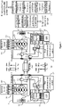
- low-speed electrical signals are represented by lines between PCs 10 and the box Slow polarization and absolute phase control 15.
- High-speed electrical signals are represented by the lines between boxes CH1 to CH4 20 and DP-IQM 25 and between CDR 30 and hybrid 35.
- Optical signals are represented by the lines between C1, C2 and C3, C4 40 and all other lines.
- Figure 1a shows the architecture of the proposed transceivers 5 at both ends of the link to realize full-duplex communication. Similar to conventional coherent transceiver, it includes a continuous wave (CW) laser 45, dual-polarization in-phase and quadrature modulator (DP-IQM) 25, and a dual polarization (DP) coherent receiver (DP-CRx) 50 realized from a 90° hybrid 35 and four balanced photodiodes 55.
- the DP-IQM 25 is driven by an electrical signal generator 60 providing four high-speed radio frequency (RF) signals depending on the modulation format employed.
- RF radio frequency
- the electrical signal generator 60 does not need to employ expensive power hungry DACs with large bit resolution (e.g. 6 or 8) since no DSP is applied on the transmitted waveforms.
- M- QAM signals can be generated by a segmented DP-IQM with each segment driven by a binary RF signal realizing an optical DAC. Since the transmitter DSP, which is illustrated in figure 1b is omitted, all system components must have adequate RF bandwidth to avoid large penalties from uncompensated inter-symbol interference (ISI). Finally, in absence of Nyquist pulse shaping, there is no control on the pulse shape of RF signals which will generally be non-bandlimited.
- DSP blocks illustrated in figure 1b are omitted, namely front-end correction and inter-symbol interference (ISI) compensation.
- ISI inter-symbol interference
- Penalty due to uncompensated ISI should be relatively small provided sufficient bandwidth.
- the absence of front end correction puts strict requirements on the front-end specifications (e.g. skew, power and phase imbalance).
- the remaining blocks in figure 1b are indispensable and cannot be ignored, namely chromatic dispersion (CD) compensation, polarization demultiplexing, carrier recovery and clock and data recovery (CDR).
- CD chromatic dispersion
- CDR clock and data recovery
- CD can be avoided by operating the system in the O-band near the single mode fiber (SMF) zero dispersion wavelength. If C band operation is favoured, optical CD compensators can replace the omitted DSP. Although optical CD compensators amenable for photonic integration are available using all-pass structures (e.g. rings), their additional insertion loss is larger than the additional propagation loss ( ⁇ 1.5 dB) incurred after 10 km in the O-band relative to the C-band. Hence, the coherent lite system is best suited for O-band operation.
- SMF single mode fiber
- transceiver 1 uses a laser 45 at ⁇ 12 that is first split; one part is modulated then passed by C1 and transmitted along the top fiber, while the other portion is passed unmodulated along the bottom fiber by C2.
- C3 and C4 pass the received signal and tone to the coherent front-end (bottom portion including components 10 and 50).
- communication in opposite direction occurs at ⁇ 21 and is allowed by the four circulators 40 and second couplers.
- Bidirectional transmission results in no penalty if ⁇ 12 and ⁇ 21 are sufficiently spaced to avoid nonlinear back scattering effects. If the signal and tone paths are almost matched, laser phase noise and frequency offset are negligible after beating in the coherent front-end and therefore DSP carrier recovery can be omitted.
- PCs optical polarization controllers
- ⁇ 1MHz low speed polarization tracking circuitry
- CDR 30 accepts the outputs from balanced photodiodes 55, extracts the clock and performs data decisions. As shown in figure 1a , a sub-clock from the recovered clock at rate R s / N , where R s is the symbol rate and N can be >1000 at 50 Gbaud, is fed back to the low speed polarization tracking circuitry 15 employing data-aided or decision-directed algorithms.
- the transceiver operative to transmit and receive optical signals.
- the transceiver comprises a laser 45 operative to generate a continuous wavelength.
- the transceiver comprises a power splitter operative to receive the continuous wavelength from the laser 45 and to split the continuous wavelength into a first portion and a second portion.
- the transceiver comprises a dual-polarization in-phase and quadrature modulator, DP-IQM, 25 operative to receive the first portion of the continuous wavelength from the power splitter and to modulate the first portion of the continuous wavelength according to a modulation format, thereby producing a first modulated signal.
- DP-IQM dual-polarization in-phase and quadrature modulator
- the transceiver comprises a first circulator C1, C3 operative to receive the first modulated signal from the DP-IQM 25 and to transmit the first modulated signal through a full-duplex fiber.
- the transceiver comprises a second circulator C2, C4 operative to receive the second portion of the continuous wavelength, which is the first unmodulated signal, from the power splitter and to transmit the first unmodulated signal through the full-duplex fiber.
- the first circulator C1, C3 being further operative to receive a second unmodulated signal from the full-duplex fiber and the second circulator C2, C4 being further operative to receive a second modulated signal from the full-duplex fiber.
- the transceiver comprises a first optical polarization controller, PC, 10 operative to receive the second unmodulated signal from the first circulator C1, C3, and to adjust a polarization state of the second unmodulated signal, thereby producing a polarization state adjusted unmodulated signal.
- the transceiver comprises a second optical polarization controller 10 operative to receive the second modulated signal from the second circulator C2, C4 and to adjust the polarization state of the second modulated signal, thereby producing a polarization state adjusted modulated signal.
- the transceiver comprises a dual-polarization coherent receiver, DP-CRx, 50 operative to receive, through a signal port, the polarization state adjusted modulated signal and, through a local oscillator port, the polarization state adjusted unmodulated signal, the DP-CRx performing coherent detection of modulating information and generating four electrical output signals.
- DP-CRx dual-polarization coherent receiver
- the DP-CRx 50 may comprise a 90° hybrid 35 connected to four balanced photodiodes 55, the 90° hybrid 35 receiving the polarization state adjusted modulated signal and the polarization state adjusted unmodulated signal through the signal port and the local oscillator port respectively, and the four balanced photodiodes 55 operative to output the four electrical output signals.
- the transceiver may further comprise an electrical signal generator 60 generating four electrical input signals for use as input to the DP-IQM 25, the four electrical input signals providing information symbols and further signals for determining a type of modulation to be performed by DP-IQM 25 to produce the first modulated signal.
- an electrical signal generator 60 generating four electrical input signals for use as input to the DP-IQM 25, the four electrical input signals providing information symbols and further signals for determining a type of modulation to be performed by DP-IQM 25 to produce the first modulated signal.
- the four electrical output signals may correspond to dual polarization in-phase quadrature signals.
- the transceiver may further comprise a clock and data recovery, CDR, 30 unit receiving the four electrical output signals, the CDR being operative to recover a clock and to perform decisions about which information symbols are received through the optical signal.
- CDR clock and data recovery
- the first and second PC 10 may be controlled by a low speed polarization tracking electrical circuit 15 which feeds a sub-clock from the recovered clock at a rate R s / N , where R s is the symbol rate and N is greater than 1000 at 50 Gbaud.
- the first transceiver is operative to transmit the first modulated signal, generated from a wavelength ⁇ 12 , through a first fiber of a fiber pair of the full-duplex fiber; transmit the first unmodulated signal, generated from the wavelength ⁇ 12 , through a second fiber of the fiber pair of the full-duplex fiber; receive the second unmodulated signal, generated from a wavelength ⁇ 21 , through the first fiber of the fiber pair of the full-duplex fiber; and receive the second modulated signal, generated from the wavelength ⁇ 21 , through the second fiber of the fiber pair of the full-duplex fiber.
- the second transceiver is operative to transmit the first unmodulated signal, generated from the wavelength ⁇ 21 , through the first fiber of the fiber pair of the full-duplex fiber; transmit the first modulated signal, generated from the wavelength ⁇ 21 , through the second fiber of the fiber pair of the full-duplex fiber; receive the second modulated signal, generated from the wavelength ⁇ 12 , through the first fiber of the fiber pair of the full-duplex fiber; and receive the second unmodulated signal, generated from the wavelength ⁇ 12 , through the second fiber of the fiber pair of the full-duplex fiber.
- Certain embodiments may provide one or more of the following technical advantage(s).
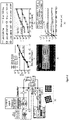
- Figure 2a shows the experimental setup in which unidirectional transmission was demonstrated, i.e. one transmitter and one receiver of the full system in figure 1a were realized. Due to unavailability of certain O-band parts at the time of the experiment, the coherent lite system was verified in the C-band. CD was compensated by an optical tunable dispersion compensator module (TDCM) to demonstrate a DSP free system and was later compared in figure 2c to DSP based CD compensation. Also, instead of using a full duplex fiber, a pair of similar fiber spools was used with desired lengths (2 or 10 km). An optical delay line was inserted in the signal path to ensure matching with the tone path.
- TDCM optical tunable dispersion compensator module
- ECL External Cavity Laser
- DFB Distributed Feedback Laser
- the DP-IQM is a commercially available Indium phosphide (InP) modulator with 3dB bandwidth of 35 GHz.
- the electrical signal generator comprised four 43 GHz RF amplifiers and generated 4-level RF signals yielding DP-16QAM.
- the 50Gbaud electrical eyediagrams is shown in the top left inset of figure 2a .
- PDs PhotoDiodes
- TIAs transimpedance amplifiers
- EDFA erbium-doped fiber amplifier
- timing recovery is performed by CDR circuit.
- a common phase rotation angle had to be estimated from the sampled waveforms and the I and Q waveforms per polarization had to be derotated with this angle. It was hypothesized that this slowly varying rotation was due to any small path length mismatch between the signal and tone paths which may vary slowly with time due to any ambient temperature and pressure changes around the two fibers spools.
- this common phase is constant during the entire captured waveform that lasts ⁇ 12.5 ⁇ s.
- the entire 50 Gbaud 16QAM waveform is depicted by the constellations in the insets of figure 2a before and after common phase derotation.
- Figure 2b shows the bit error rate (BER) versus baud rate in back-to-back for 16QAM in two scenarios: single and dual polarization (SP and DP) transmission where the BER is counted per polarization.
- SP and DP single and dual polarization
- This figure shows no penalty arising from DP transmission compared to SP, i.e. polarization demultiplexing is properly achieved optically. For later results, average BER of the two polarizations is reported for DP case.
- figure 2c compares the DSP-free performance obtained with the TDCM at 2 and 10 km with two cases in which TDCM was removed: i) only CD is compensated digitally, ii) the full DSP stack of figure 1b is applied including ISI compensation.
- figure 2e shows the effect of mismatch between tone and signal paths on the BER of 50 Gbaud 16QAM in B2B.
- Three 15.5 dBm lasers with different linewidths were compared.
- the system tolerates huge mismatches up to 6 m.
- the system still tolerates 25 cm of mismatch without DSP carrier recovery.
- a DSP-free coherent lite transceiver that circumvents high-speed, highresolution DACs and ADCs for 10 km intra-DC optics is proposed.
- the proposed transceiver architecture can be fully integrated on chip and can exploit low cost DFB lasers.
- 1.6 Tb/s aggregate capacity can be realized below KP4 FEC after 10 km.
Landscapes
- Engineering & Computer Science (AREA)
- Computer Networks & Wireless Communication (AREA)
- Signal Processing (AREA)
- Physics & Mathematics (AREA)
- Electromagnetism (AREA)
- Optical Communication System (AREA)
Description
- The present disclosure relates to data transmission through optic fiber and more specifically to transceivers for the data transmission and reception.
- Datacenter (DC) traffic, of which >75% stays within the same DC, is growing steadily. This is generating immense need for fast inexpensive power efficient intra-DC optics operating over 10 km. Ethernet speed is envisioned to reach 1.6 Tb/s after 2020 thus spectrally efficient high order modulation is essential to push the capacity per channel or carrier and multiplex fewer channels to achieve aggregate capacity. Various low-cost >10km demonstrations at >200 Gb/s per channel or color were achieved. In parallel, coherent detection used in metro and long haul links enables high spectral efficiency by giving access to all four degrees of freedom on the optical carrier while providing superior sensitivity relative to direct detection. Some of the existing solutions are regarded as too expensive and power hungry for short reach optics.
-
US 2016/261346 A1 discloses an apparatus comprising an uncooled laser, a splitter coupled to the laser, a first wavelength component coupled to the splitter, a local oscillator (LO) port coupled to the first wavelength component, a modulator coupled to the splitter, a second wavelength component coupled to the modulator, and a signal port coupled to the second wavelength component. A method comprises emitting an input light, splitting the input light into a first local oscillator (LO) optical signal and a first unmodulated optical signal, modulating the first unmodulated optical signal using polarization-multiplexed, high-order modulation to produce a first modulated optical signal, transmitting the first LO optical signal to a first duplex fiber, and transmitting the first modulated optical signal to a second duplex fiber. - There is provided a transceiver operative to transmit and receive optical signals. The transceiver comprises a laser operative to generate a continuous wavelength. The transceiver comprises a power splitter operative to receive the continuous wavelength from the laser and to split the continuous wavelength into a first portion and a second portion. The transceiver comprises a dual-polarization inphase and quadrature modulator, DP-IQM, operative to receive the first portion of the continuous wavelength from the power splitter and to modulate the first portion of the continuous wavelength according to a modulation format, thereby producing a first modulated signal. The transceiver comprises a first circulator (C1, C3) operative to receive the first modulated signal from the DP-IQM and to transmit the first modulated signal through a full-duplex fiber. The transceiver comprises a second circulator (C2, C4) operative to receive the second portion of the continuous wavelength, which is the first unmodulated signal, from the power splitter and to transmit the first unmodulated signal through the full-duplex fiber. The first circulator (C1, C3) is further operative to receive a second unmodulated signal from the full-duplex fiber and the second circulator (C2, C4) is further operative to receive a second modulated signal from the full-duplex fiber. The transceiver comprises a first optical polarization controller, PC, operative to receive the second unmodulated signal from the first circulator (C1, C3), and to adjust a polarization state of the second unmodulated signal, thereby producing a polarization state adjusted unmodulated signal. The transceiver comprises a second optical polarization controller operative to receive the second modulated signal from the second circulator (C2, C4) and to adjust the polarization state of the second modulated signal, thereby producing a polarization state adjusted modulated signal. The transceiver comprises a dual-polarization coherent receiver, DP-CRx, operative to receive, through a signal port, the polarization state adjusted modulated signal and, through a local oscillator port, the polarization state adjusted unmodulated signal, the DP-CRx performing coherent detection of modulating information and generating four electrical output signals.
- The DP-CRx may comprise a 90° hybrid connected to four balanced photodiodes, the 90° hybrid receiving the polarization state adjusted modulated signal and the polarization state adjusted unmodulated signal through the signal port and the local oscillator port respectively, and the four balanced photodiodes operative to output the four electrical output signals.
- The transceiver may further comprise an electrical signal generator generating four electrical input signals for use as input to the DP-IQM, the four electrical input signals providing information symbols and further signals for determining a type of modulation to be performed by DP-IQM to produce the first modulated signal.
- The four electrical output signals may correspond to dual polarization in-phase quadrature signals.
- The transceiver may further comprise a clock and data recovery, CDR, unit receiving the four electrical output signals, the CDR being operative to recover a clock and to perform decisions about which information symbols are received through the optical signal.
- The first and second PC may be controlled by a low speed polarization tracking electrical circuit which feeds a sub-clock from the recovered clock at a rate Rs/N, where R s is the symbol rate and N is greater than1000 at 50 Gbaud.
- There is provided a system comprising a first transceiver and a second transceiver as described previously. The first transceiver is operative to transmit the first modulated signal, generated from a wavelength λ12, through a first fiber of a fiber pair of the full-duplex fiber; transmit the first unmodulated signal, generated from the wavelength λ12, through a second fiber of the fiber pair of the full-duplex fiber; receive the second unmodulated signal, generated from a wavelength λ21, through the first fiber of the fiber pair of the full-duplex fiber; and receive the second modulated signal, generated from the wavelength λ21, through the second fiber of the fiber pair of the full-duplex fiber. The second transceiver is operative to transmit the first unmodulated signal, generated from the wavelength λ21, through the first fiber of the fiber pair of the full-duplex fiber; transmit the first modulated signal, generated from the wavelength λ21, through the second fiber of the fiber pair of the full-duplex fiber; receive the second modulated signal, generated from the wavelength λ12, through the first fiber of the fiber pair of the full-duplex fiber; and receive the second unmodulated signal, generated from the wavelength λ12, through the second fiber of the fiber pair of the full-duplex fiber.
- The transceivers provided herein present improvements to the way transceivers operate.
-
-
Figure 1a is a schematic illustration of coherent-lite transceivers configured for full-duplex transmission using according to an example embodiment. -
Figure 1b is a schematic illustration of legacy coherent digital signal processor (DSP) that are omitted in the coherent-lite transceiver (left: transmitter DSP, right: receiver DSP excluding fiber nonlinearity migration). -
Figure 2a is a schematic illustration of an experimental setup according to an example embodiment. -
Figure 2b is a graph of bit-error-rate (BER) versus baud rate for dual polarization (DP)-16 quadrature amplitude modulation (QAM) in back-to-back (B2B) for DP and single polarization (SP) transmission. -
Figure 2c is a graph of BER versus baud rate for DP-16QAM after 2 and 10 km, comparing DSP-free, DSP chromatic dispersion (CD) compensation and full DSP performance. -
Figure 2d is a picture of Raw unequalized 50 Gbaud 4-level eyediagram of one received quadrature from a Keysight pulse-amplitude modulation (PAM)-4 analysis tool. -
Figure 2e is a graph of BER of 50Gbaud 16QAM in B2B versus mismatch between tone and signal paths for three different lasers. - Some of the embodiments contemplated herein will now be described more fully with reference to the accompanying drawings. Other embodiments, however, are contained within the scope of the subject matter disclosed herein, the disclosed subject matter should not be construed as limited to only the embodiments set forth herein; rather, these embodiments are provided by way of example to convey the scope of the subject matter to those skilled in the art.
- Generally, all terms used herein are to be interpreted according to their ordinary meaning in the relevant technical field, unless a different meaning is clearly given and/or is implied from the context in which it is used. All references to a/an/the element, apparatus, component, means, step, etc. are to be interpreted openly as referring to at least one instance of the element, apparatus, component, means, step, etc., unless explicitly stated otherwise. The steps of any methods disclosed herein do not have to be performed in the exact order disclosed, unless a step is explicitly described as following or preceding another step and/or where it is implicit that a step must follow or precede another step. Any feature of any of the embodiments disclosed herein may be applied to any other embodiment, wherever appropriate. Likewise, any advantage of any of the embodiments may apply to any other embodiments, and vice versa. Other objectives, features and advantages of the enclosed embodiments will be apparent from the following description.
- Certain aspects of the present disclosure and their embodiments may provide solutions to overcome the fact that existing solutions are too expensive and power hungry for short reach optics. There is proposed a power efficient optical intra-DC "coherent lite" transceiver that requires neither high speed DSP nor high resolution data converters. The proposed coherent lite transceiver was experimentally validated as achieving 50 Gbaud DP-16QAM, DP standing for dual polarization and QAM standing for quadrature amplitude modulation, yielding 400 Gb/s over 10 km below the 2.2×10⁻⁴ KP4 forward error correction (FEC) threshold. FEC stands for forward error correction, which is coding done to detect and correct random and burst errors within a received bit stream. KP4 is a term used to denote a certain FEC code called the Reed-Solomon RS(544,514) code because this code is standardized for use in 100Gb/s backplane applications denoted 100GBASE-KP4 within the Ethernet standard.
- Referring to
figure 1a , the proposed coherent lite transceiver 5 is eliminating transmitter and receiver digital signal processor (DSP) conventionally required in a legacy coherent transceiver. Hence, power hungry, high-speed, high resolution digital-to-analog and analog-to-digital converters (DACs and ADCs) are no longer required along with application specific integrated circuits (ASIC) that perform DSP. In the proposed coherent lite system, conventional coherent DSP functions that are detailed infigure 1b are either discarded, possibly resulting in performance penalty, or replaced by an optical component. Henceforth, it is explained how the impairments corrected by DSP infigure 1b are dealt with in the proposed coherent lite system. - In
figure 1a , low-speed electrical signals are represented by lines betweenPCs 10 and the box Slow polarization andabsolute phase control 15. High-speed electrical signals are represented by the lines between boxes CH1 toCH4 20 and DP-IQM 25 and betweenCDR 30 andhybrid 35. Optical signals are represented by the lines between C1, C2 and C3,C4 40 and all other lines. -
Figure 1a shows the architecture of the proposed transceivers 5 at both ends of the link to realize full-duplex communication. Similar to conventional coherent transceiver, it includes a continuous wave (CW)laser 45, dual-polarization in-phase and quadrature modulator (DP-IQM) 25, and a dual polarization (DP) coherent receiver (DP-CRx) 50 realized from a 90°hybrid 35 and fourbalanced photodiodes 55. The DP-IQM 25 is driven by anelectrical signal generator 60 providing four high-speed radio frequency (RF) signals depending on the modulation format employed. In principle, theelectrical signal generator 60 does not need to employ expensive power hungry DACs with large bit resolution (e.g. 6 or 8) since no DSP is applied on the transmitted waveforms. - Producing four multilevel RF signal each with


figure 1b is omitted, all system components must have adequate RF bandwidth to avoid large penalties from uncompensated inter-symbol interference (ISI). Finally, in absence of Nyquist pulse shaping, there is no control on the pulse shape of RF signals which will generally be non-bandlimited. - At the receiver, some DSP blocks illustrated in
figure 1b are omitted, namely front-end correction and inter-symbol interference (ISI) compensation. Penalty due to uncompensated ISI should be relatively small provided sufficient bandwidth. In addition, the absence of front end correction puts strict requirements on the front-end specifications (e.g. skew, power and phase imbalance). Finally, the remaining blocks infigure 1b are indispensable and cannot be ignored, namely chromatic dispersion (CD) compensation, polarization demultiplexing, carrier recovery and clock and data recovery (CDR). - CD can be avoided by operating the system in the O-band near the single mode fiber (SMF) zero dispersion wavelength. If C band operation is favoured, optical CD compensators can replace the omitted DSP. Although optical CD compensators amenable for photonic integration are available using all-pass structures (e.g. rings), their additional insertion loss is larger than the additional propagation loss (~ 1.5 dB) incurred after 10 km in the O-band relative to the C-band. Hence, the coherent lite system is best suited for O-band operation.
- Next, removal of the carrier recovery DSP is accounted for by using a self-homodyne approach. The main idea is to make use of the full-duplex fiber that is readily deployed in intra-DC links (<10 km) to transmit the modulated signal and a copy of the transmit laser on the fiber pair of full-duplex fiber. This is achieved via the four circulators C1 to
C4 40 and the two couplers depicted infigure 1a . For example,transceiver 1 uses alaser 45 at λ12 that is first split; one part is modulated then passed by C1 and transmitted along the top fiber, while the other portion is passed unmodulated along the bottom fiber by C2. Attransceiver 2, C3 and C4 pass the received signal and tone to the coherent front-end (bottomportion including components 10 and 50). Likewise, communication in opposite direction occurs at λ21 and is allowed by the fourcirculators 40 and second couplers. Bidirectional transmission results in no penalty if λ12 and λ21 are sufficiently spaced to avoid nonlinear back scattering effects. If the signal and tone paths are almost matched, laser phase noise and frequency offset are negligible after beating in the coherent front-end and therefore DSP carrier recovery can be omitted. - Next, the polarization demultiplexing DSP is replaced by optical polarization controllers (PCs) 10 in both the tone and signal paths driven by low speed polarization tracking circuitry (<1MHz). Because photonic integrated electrically controllable PCs have been realized by couplers and phase shifters, inserting them on chip before a coherent front-end achieves the necessary polarization demultiplexing.
- Finally,
CDR 30 accepts the outputs frombalanced photodiodes 55, extracts the clock and performs data decisions. As shown infigure 1a , a sub-clock from the recovered clock at rate Rs/N, where R s is the symbol rate and N can be >1000 at 50 Gbaud, is fed back to the low speedpolarization tracking circuitry 15 employing data-aided or decision-directed algorithms. - There is provided a transceiver operative to transmit and receive optical signals. The transceiver comprises a
laser 45 operative to generate a continuous wavelength. The transceiver comprises a power splitter operative to receive the continuous wavelength from thelaser 45 and to split the continuous wavelength into a first portion and a second portion. The transceiver comprises a dual-polarization in-phase and quadrature modulator, DP-IQM, 25 operative to receive the first portion of the continuous wavelength from the power splitter and to modulate the first portion of the continuous wavelength according to a modulation format, thereby producing a first modulated signal. The transceiver comprises a first circulator C1, C3 operative to receive the first modulated signal from the DP-IQM 25 and to transmit the first modulated signal through a full-duplex fiber. The transceiver comprises a second circulator C2, C4 operative to receive the second portion of the continuous wavelength, which is the first unmodulated signal, from the power splitter and to transmit the first unmodulated signal through the full-duplex fiber. The first circulator C1, C3 being further operative to receive a second unmodulated signal from the full-duplex fiber and the second circulator C2, C4 being further operative to receive a second modulated signal from the full-duplex fiber. The transceiver comprises a first optical polarization controller, PC, 10 operative to receive the second unmodulated signal from the first circulator C1, C3, and to adjust a polarization state of the second unmodulated signal, thereby producing a polarization state adjusted unmodulated signal. The transceiver comprises a secondoptical polarization controller 10 operative to receive the second modulated signal from the second circulator C2, C4 and to adjust the polarization state of the second modulated signal, thereby producing a polarization state adjusted modulated signal. The transceiver comprises a dual-polarization coherent receiver, DP-CRx, 50 operative to receive, through a signal port, the polarization state adjusted modulated signal and, through a local oscillator port, the polarization state adjusted unmodulated signal, the DP-CRx performing coherent detection of modulating information and generating four electrical output signals. - The DP-
CRx 50 may comprise a 90°hybrid 35 connected to fourbalanced photodiodes 55, the 90°hybrid 35 receiving the polarization state adjusted modulated signal and the polarization state adjusted unmodulated signal through the signal port and the local oscillator port respectively, and the fourbalanced photodiodes 55 operative to output the four electrical output signals. - The transceiver may further comprise an
electrical signal generator 60 generating four electrical input signals for use as input to the DP-IQM 25, the four electrical input signals providing information symbols and further signals for determining a type of modulation to be performed by DP-IQM 25 to produce the first modulated signal. - The four electrical output signals may correspond to dual polarization in-phase quadrature signals.
- The transceiver may further comprise a clock and data recovery, CDR, 30 unit receiving the four electrical output signals, the CDR being operative to recover a clock and to perform decisions about which information symbols are received through the optical signal.
- The first and
second PC 10 may be controlled by a low speed polarization trackingelectrical circuit 15 which feeds a sub-clock from the recovered clock at a rate Rs/N, where R s is the symbol rate and N is greater than 1000 at 50 Gbaud. - There is provided a system comprising a first and a second transceiver 5 as described previously. The first transceiver is operative to transmit the first modulated signal, generated from a wavelength λ12, through a first fiber of a fiber pair of the full-duplex fiber; transmit the first unmodulated signal, generated from the wavelength λ12, through a second fiber of the fiber pair of the full-duplex fiber; receive the second unmodulated signal, generated from a wavelength λ21, through the first fiber of the fiber pair of the full-duplex fiber; and receive the second modulated signal, generated from the wavelength λ21, through the second fiber of the fiber pair of the full-duplex fiber. The second transceiver is operative to transmit the first unmodulated signal, generated from the wavelength λ21, through the first fiber of the fiber pair of the full-duplex fiber; transmit the first modulated signal, generated from the wavelength λ21, through the second fiber of the fiber pair of the full-duplex fiber; receive the second modulated signal, generated from the wavelength λ12, through the first fiber of the fiber pair of the full-duplex fiber; and receive the second unmodulated signal, generated from the wavelength λ12, through the second fiber of the fiber pair of the full-duplex fiber.
- Certain embodiments may provide one or more of the following technical advantage(s).
- a) The proposed coherent-lite transceiver provides access to all available four degrees of freedom on the optical field and hence yields high spectral efficiency similar to a conventional coherent transceiver. Spectral efficiency being the ratio of transmitted bit rate to bandwidth occupied for transmission.
- b) The proposed coherent-lite transceiver is DSP-free, i.e. there is no need to carry out any digital signal processing at the transmitter and receiver sides to mitigate the transmission impairments.
- c) Since the proposed coherent-lite transceiver is DSP-free, high speed application specific integrated circuits (ASICs) that carry out the DSP are no longer needed.
- d) Also since the proposed coherent-lite transceiver is DSP-free, high speed digital-to-analog converters (DACs) and analog-to-digital converters (ADCs) are also not required.
- e) Removing the DSP-ASIC, DAC, ADC makes the proposed transceiver cheaper and also reduces the power consumption. Cost and power consumption are very important drivers for the short-reach intradatacenter applications targeted by this transceiver.
-
Figure 2a shows the experimental setup in which unidirectional transmission was demonstrated, i.e. one transmitter and one receiver of the full system infigure 1a were realized. Due to unavailability of certain O-band parts at the time of the experiment, the coherent lite system was verified in the C-band. CD was compensated by an optical tunable dispersion compensator module (TDCM) to demonstrate a DSP free system and was later compared infigure 2c to DSP based CD compensation. Also, instead of using a full duplex fiber, a pair of similar fiber spools was used with desired lengths (2 or 10 km). An optical delay line was inserted in the signal path to ensure matching with the tone path. A 15.5 dBm External Cavity Laser (ECL) with linewidth <100 kHz was used in all measurements except for the last part where two different Distributed Feedback Laser (DFB) lasers were also used to examine the linewidths tolerance infigure 2e . - The DP-IQM is a commercially available Indium phosphide (InP) modulator with 3dB bandwidth of 35 GHz. The electrical signal generator comprised four 43 GHz RF amplifiers and generated 4-level RF signals yielding DP-16QAM. The 50Gbaud electrical eyediagrams is shown in the top left inset of
figure 2a . At the receiver, four 40 GHz balanced PhotoDiodes (PDs) follow the DP hybrid. Due to unavailability of balanced PDs with transimpedance amplifiers (TIAs), an erbium-doped fiber amplifier (EDFA) was used in the signal path prior to the Coherent receiver (CRx), however the tone path was unamplified. Manual PCs were used in both signal and tone paths because the polarization state was stable enough in the lab environment. Two 63 GHz real-time scopes (RTOs) sampled the outputs of balanced photodiodes at 160 Giga samples per second (GSa/s) for offline error counting. Resampling and timing recovery were performed offline on the sampled waveforms before error counting. - In a real time coherent-lite receiver, timing recovery is performed by CDR circuit. In addition to timing recovery, a common phase rotation angle had to be estimated from the sampled waveforms and the I and Q waveforms per polarization had to be derotated with this angle. It was hypothesized that this slowly varying rotation was due to any small path length mismatch between the signal and tone paths which may vary slowly with time due to any ambient temperature and pressure changes around the two fibers spools. However, this common phase is constant during the entire captured waveform that lasts ~12.5 µs. The entire 50 Gbaud 16QAM waveform is depicted by the constellations in the insets of
figure 2a before and after common phase derotation. Other than that, no DSP is applied at the receiver to obtain these constellations after 2km. The real-time raw unequalized 4-level eyediagram of one quadrature obtained on the RTO by the Keysight PAM4 analysis tool is also shown infigure 2d . In a real time coherent-lite receiver, the slowly varying phase derotation can be achieved by the electrically controlled PCs depicted infigure 1a (provided they have three stages of variable phase shifters). -
Figure 2b shows the bit error rate (BER) versus baud rate in back-to-back for 16QAM in two scenarios: single and dual polarization (SP and DP) transmission where the BER is counted per polarization. This figure shows no penalty arising from DP transmission compared to SP, i.e. polarization demultiplexing is properly achieved optically. For later results, average BER of the two polarizations is reported for DP case. Next,figure 2c compares the DSP-free performance obtained with the TDCM at 2 and 10 km with two cases in which TDCM was removed: i) only CD is compensated digitally, ii) the full DSP stack offigure 1b is applied including ISI compensation. No significant difference between compensating CD optically or digitally is noticed. Also, results confirm DSP-free 400 Gb/s 10 km transmission below the KP4 FEC threshold. Further, compensating residual ISI by leveraging the full DSP stack improves the BER by an order of magnitude and pushes capacity below KP4 FEC to 512 Gb/s (64 Gbaud). - Finally,
figure 2e shows the effect of mismatch between tone and signal paths on the BER of 50 Gbaud 16QAM in B2B. Three 15.5 dBm lasers with different linewidths were compared. With the ECL, the system tolerates huge mismatches up to 6 m. With 350 kHz DFB laser, the system still tolerates 25 cm of mismatch without DSP carrier recovery. - In conclusion, a DSP-free coherent lite transceiver that circumvents high-speed, highresolution DACs and ADCs for 10 km intra-DC optics is proposed. The proposed transceiver architecture can be fully integrated on chip and can exploit low cost DFB lasers. By replicating the 400 Gb/s single color experimental demonstration on four multiplexed wavelengths, 1.6 Tb/s aggregate capacity can be realized below KP4 FEC after 10 km.
Claims (7)
- A transceiver operative to transmit and receive optical signals, comprising:- a laser (45) operative to generate a continuous wavelength;- a power splitter operative to receive the continuous wavelength from the laser (45) and to split the continuous wavelength into a first portion and a second portion;- a dual-polarization in-phase and quadrature modulator, DP-IQM, (25) operative to receive the first portion of the continuous wavelength from the power splitter and to modulate the first portion of the continuous wavelength according to a modulation format, thereby producing a first modulated signal;- a first circulator (C1, C3) operative to receive the first modulated signal from the DP-IQM (25) and to transmit the first modulated signal through a full-duplex fiber;- a second circulator (C2, C4) operative to receive the second portion of the continuous wavelength, which is the first unmodulated signal, from the power splitter and to transmit the first unmodulated signal through the full-duplex fiber;the first circulator (C1, C3) being further operative to receive a second unmodulated signal from the full-duplex fiber and the second circulator (C2, C4) being further operative to receive a second modulated signal from the full-duplex fiber;- a first optical polarization controller, PC, (10) operative to receive the second unmodulated signal from the first circulator (C1, C3), and to adjust a polarization state of the second unmodulated signal, thereby producing a polarization state adjusted unmodulated signal;- a second optical polarization controller (10) operative to receive the second modulated signal from the second circulator (C2, C4) and to adjust the polarization state of the second modulated signal, thereby producing a polarization state adjusted modulated signal; and- a dual-polarization coherent receiver, DP-CRx, (50) operative to receive, through a signal port, the polarization state adjusted modulated signal and, through a local oscillator port, the polarization state adjusted unmodulated signal, the DP-CRx being configured to perform coherent detection of modulating information and to generate four electrical output signals.
- The transceiver of claim 1, wherein the DP-CRx (50) comprises a 90° hybrid (35) connected to four balanced photodiodes (55), the 90° hybrid (35) being configured to receive the polarization state adjusted modulated signal and the polarization state adjusted unmodulated signal through the signal port and the local oscillator port respectively, and the four balanced photodiodes (55) being operative to output the four electrical output signals.
- The transceiver of claim 1 or 2, further comprising an electrical signal generator (60) being configured to generate four electrical input signals for use as input to the DP-IQM (25), the four electrical input signals providing information symbols and further signals for determining a type of modulation to be performed by DP-IQM (25) to produce the first modulated signal.
- The transceiver of any one of claims 1 to 3, wherein the four electrical output signals correspond to dual polarization in-phase quadrature signals.
- The transceiver of any one of claim 1 to 4, further comprising a clock and data recovery, CDR, (30) unit being configured to receive the four electrical output signals, the CDR being operative to recover a clock and to perform decisions about which information symbols are received through the optical signal.
- The transceiver of claim 5, wherein the first and second PC (10) are configured to be controlled by a low speed polarization tracking electrical circuit (15) which is configured to feed a sub-clock from the recovered clock at a rate Rs/N, where R s is the symbol rate and N is greater than1000 at 50 Gbaud.
- A system comprising:- a first transceiver according to any one of claims 1-6, wherein the first transceiver is operative to:∘ transmit the first modulated signal, generated from a wavelength λ12, through a first fiber of a fiber pair of the full-duplex fiber;∘ transmit the first unmodulated signal, generated from the wavelength λ12, through a second fiber of the fiber pair of the full-duplex fiber;∘ receive the second unmodulated signal, generated from a wavelength λ21, through the first fiber of the fiber pair of the full-duplex fiber; and∘ receive the second modulated signal, generated from the wavelength λ21, through the second fiber of the fiber pair of the full-duplex fiber; and- a second transceiver according to any one of claims 1-6, wherein the second transceiver is operative to:∘ transmit the first unmodulated signal, generated from the wavelength λ21, through the first fiber of the fiber pair of the full-duplex fiber;∘ transmit the first modulated signal, generated from the wavelength λ21, through the second fiber of the fiber pair of the full-duplex fiber;∘ receive the second modulated signal, generated from the wavelength λ12, through the first fiber of the fiber pair of the full-duplex fiber; and∘ receive the second unmodulated signal, generated from the wavelength λ12, through the second fiber of the fiber pair of the full-duplex fiber.
Applications Claiming Priority (2)
| Application Number | Priority Date | Filing Date | Title |
|---|---|---|---|
| US201762554267P | 2017-09-05 | 2017-09-05 | |
| PCT/IB2018/056754 WO2019049030A1 (en) | 2017-09-05 | 2018-09-04 | A dsp-free 'coherent lite' transceiver for next generation 1 lambda × 400g 10km optical intra-datacenter interconnects |
Publications (2)
| Publication Number | Publication Date |
|---|---|
| EP3679661A1 EP3679661A1 (en) | 2020-07-15 |
| EP3679661B1 true EP3679661B1 (en) | 2022-06-22 |
Family
ID=63683261
Family Applications (1)
| Application Number | Title | Priority Date | Filing Date |
|---|---|---|---|
| EP18774142.6A Active EP3679661B1 (en) | 2017-09-05 | 2018-09-04 | A dsp-free 'coherent lite' transceiver for next generation 1 lambda × 400g 10km optical intra-datacenter interconnects |
Country Status (3)
| Country | Link |
|---|---|
| US (1) | US11228371B2 (en) |
| EP (1) | EP3679661B1 (en) |
| WO (1) | WO2019049030A1 (en) |
Families Citing this family (10)
| Publication number | Priority date | Publication date | Assignee | Title |
|---|---|---|---|---|
| US10917175B2 (en) * | 2017-11-21 | 2021-02-09 | Cable Television Laboratories, Inc. | Systems and methods for full duplex coherent optics |
| US10735097B2 (en) * | 2017-11-21 | 2020-08-04 | Cable Television Laboratories, Inc | Systems and methods for full duplex coherent optics |
| CN111064525B (en) * | 2019-12-26 | 2022-04-01 | 山东大学 | Optical transmission system for data center internal interconnection based on wired-wireless fusion and operation method thereof |
| CN113132020B (en) * | 2019-12-31 | 2023-07-28 | 华为技术有限公司 | Coherent light receiving device and optical system using coherent light receiving device |
| CN114430297B (en) * | 2020-10-29 | 2025-08-29 | 华为技术有限公司 | Optical transmission equipment and systems |
| US12388529B2 (en) * | 2021-03-19 | 2025-08-12 | Infinera Corp. | State of polarization sensitive coherent optical time domain reflectometry |
| US12442681B2 (en) * | 2021-10-18 | 2025-10-14 | Nec Corporation | Distributed fiber optic sensing enabled self-coherent detection for data centers |
| US12147078B2 (en) * | 2022-11-11 | 2024-11-19 | Lightmatter, Inc. | Polarization locker for fiber connections and related methods |
| CN117155477A (en) * | 2023-10-07 | 2023-12-01 | 西湖大学 | DSP-free short-range coherent receiving system and method of frequency quasi-synchronous optical network architecture |
| CN117278076B (en) * | 2023-11-24 | 2024-03-19 | 中铁通信信号勘测设计院有限公司 | Communication transmission method and system for fusion of power carrier and Ethernet |
Family Cites Families (5)
| Publication number | Priority date | Publication date | Assignee | Title |
|---|---|---|---|---|
| GB8709073D0 (en) * | 1987-04-15 | 1987-05-20 | British Telecomm | Coherent optical systems |
| US9438348B2 (en) | 2014-11-06 | 2016-09-06 | Alcatel Lucent | Communication method for a cluster of network hosts |
| US10050713B2 (en) * | 2015-03-02 | 2018-08-14 | Futurewei Technologies, Inc. | Optical transceiver using duplex media, self-homodyne detection (SHD), coherent detection, and uncooled laser |
| EP3269055B1 (en) * | 2015-04-09 | 2019-12-25 | Huawei Technologies Co. Ltd. | Optical transceiving using self-homodyne detection (shd) and remote modulation |
| US10651820B2 (en) | 2016-09-16 | 2020-05-12 | Ecole Polytechnique Federale De Lausanne (Epfl) | Signal processing apparatus and method for transmitting and receiving coherent parallel optical signals |
-
2018
- 2018-09-04 US US16/642,643 patent/US11228371B2/en not_active Expired - Fee Related
- 2018-09-04 WO PCT/IB2018/056754 patent/WO2019049030A1/en not_active Ceased
- 2018-09-04 EP EP18774142.6A patent/EP3679661B1/en active Active
Also Published As
| Publication number | Publication date |
|---|---|
| WO2019049030A1 (en) | 2019-03-14 |
| US11228371B2 (en) | 2022-01-18 |
| US20210159983A1 (en) | 2021-05-27 |
| EP3679661A1 (en) | 2020-07-15 |
Similar Documents
| Publication | Publication Date | Title |
|---|---|---|
| US11228371B2 (en) | DSP-free ‘coherent lite’ transceiver for next generation 1 lambda x 400G 10km optical intra-datacenter interconnects | |
| US8086109B2 (en) | Polarization multiplexed optical transmitting and receiving apparatus | |
| US10284323B2 (en) | Optical transceiver with external laser source | |
| EP2420011B1 (en) | Method of and system for detecting skew between parallel signals | |
| Sowailem et al. | Self-homodyne system for next generation intra-datacenter optical interconnects | |
| US9692519B2 (en) | Level spacing for M-PAM optical systems with coherent detection | |
| Che et al. | 2.4-Tb/s single-wavelength coherent transmission enabled by 114-GHz all-electronic digital-band-interleaved DACs | |
| US9294192B2 (en) | Method, system, and transceiver device for bi-directionally transmitting digital optical signals over an optical transmission link | |
| US20190319712A1 (en) | Amplitude coherent detection for pulse amplitude modulation signals | |
| US20130195455A1 (en) | Method and device for transmission and reception of a polarization multiplexed optical signal | |
| US20080056727A1 (en) | Optical transmitter and drive method of same | |
| Plant et al. | Optical communication systems for datacenter networks | |
| Almonacil et al. | 260-GBaud single-wavelength coherent transmission over 100-km SSMF based on novel arbitrary waveform generator and thin-film niobate I/Q modulator | |
| US9692521B1 (en) | Polarization pre-compensation technique for polarization-division-multiplexed direct-detection optical communication systems | |
| Bissessur et al. | Real-Time Unrepeatered C-Band Transmission of 30.5 Tb/s over 276.4 km and 29.45 Tb/s over 292.5 km | |
| Rios-Muller et al. | Experimental comparison between hybrid-QPSK/8QAM and 4D-32SP-16QAM formats at 31.2 GBaud using Nyquist pulse shaping | |
| CN110278036B (en) | Digital coherent transceiver applied to data center, data transmission method and device | |
| JP5068240B2 (en) | Optical transmission system, transmitter and receiver | |
| EP2873182B1 (en) | Method and device for signal processing in an optical communication network | |
| US20140241722A1 (en) | PDM-(M) Ask Optical Systems And Methods For Metro Network Applications | |
| US20230336248A1 (en) | Reconfigurable optical transceiver for use with multiple modulation techniques | |
| US9819415B2 (en) | Interference cancellation device and interference cancellation method | |
| Ji et al. | Complementary polarization-diversity self-coherent homodyne receiver with rapid polarization tracking for remote LO | |
| Huang et al. | Beyond 800 GB/s transmission demonstration using carrierless phase retrieval reception | |
| Nakamura et al. | 30-Gbps (5-Gsymbol/s) 64-QAM self-homodyne transmission over 60-km SSMF using phase-noise cancelling technique and ISI-suppression based on electronic digital processing |
Legal Events
| Date | Code | Title | Description |
|---|---|---|---|
| STAA | Information on the status of an ep patent application or granted ep patent |
Free format text: STATUS: UNKNOWN |
|
| STAA | Information on the status of an ep patent application or granted ep patent |
Free format text: STATUS: THE INTERNATIONAL PUBLICATION HAS BEEN MADE |
|
| PUAI | Public reference made under article 153(3) epc to a published international application that has entered the european phase |
Free format text: ORIGINAL CODE: 0009012 |
|
| STAA | Information on the status of an ep patent application or granted ep patent |
Free format text: STATUS: REQUEST FOR EXAMINATION WAS MADE |
|
| 17P | Request for examination filed |
Effective date: 20200324 |
|
| AK | Designated contracting states |
Kind code of ref document: A1 Designated state(s): AL AT BE BG CH CY CZ DE DK EE ES FI FR GB GR HR HU IE IS IT LI LT LU LV MC MK MT NL NO PL PT RO RS SE SI SK SM TR |
|
| AX | Request for extension of the european patent |
Extension state: BA ME |
|
| DAV | Request for validation of the european patent (deleted) | ||
| DAX | Request for extension of the european patent (deleted) | ||
| GRAP | Despatch of communication of intention to grant a patent |
Free format text: ORIGINAL CODE: EPIDOSNIGR1 |
|
| STAA | Information on the status of an ep patent application or granted ep patent |
Free format text: STATUS: GRANT OF PATENT IS INTENDED |
|
| INTG | Intention to grant announced |
Effective date: 20220217 |
|
| GRAS | Grant fee paid |
Free format text: ORIGINAL CODE: EPIDOSNIGR3 |
|
| GRAA | (expected) grant |
Free format text: ORIGINAL CODE: 0009210 |
|
| STAA | Information on the status of an ep patent application or granted ep patent |
Free format text: STATUS: THE PATENT HAS BEEN GRANTED |
|
| AK | Designated contracting states |
Kind code of ref document: B1 Designated state(s): AL AT BE BG CH CY CZ DE DK EE ES FI FR GB GR HR HU IE IS IT LI LT LU LV MC MK MT NL NO PL PT RO RS SE SI SK SM TR |
|
| REG | Reference to a national code |
Ref country code: GB Ref legal event code: FG4D |
|
| REG | Reference to a national code |
Ref country code: CH Ref legal event code: EP |
|
| REG | Reference to a national code |
Ref country code: DE Ref legal event code: R096 Ref document number: 602018037055 Country of ref document: DE |
|
| REG | Reference to a national code |
Ref country code: AT Ref legal event code: REF Ref document number: 1500473 Country of ref document: AT Kind code of ref document: T Effective date: 20220715 |
|
| REG | Reference to a national code |
Ref country code: IE Ref legal event code: FG4D |
|
| REG | Reference to a national code |
Ref country code: LT Ref legal event code: MG9D |
|
| REG | Reference to a national code |
Ref country code: NL Ref legal event code: MP Effective date: 20220622 |
|
| PG25 | Lapsed in a contracting state [announced via postgrant information from national office to epo] |
Ref country code: SE Free format text: LAPSE BECAUSE OF FAILURE TO SUBMIT A TRANSLATION OF THE DESCRIPTION OR TO PAY THE FEE WITHIN THE PRESCRIBED TIME-LIMIT Effective date: 20220622 Ref country code: NO Free format text: LAPSE BECAUSE OF FAILURE TO SUBMIT A TRANSLATION OF THE DESCRIPTION OR TO PAY THE FEE WITHIN THE PRESCRIBED TIME-LIMIT Effective date: 20220922 Ref country code: LT Free format text: LAPSE BECAUSE OF FAILURE TO SUBMIT A TRANSLATION OF THE DESCRIPTION OR TO PAY THE FEE WITHIN THE PRESCRIBED TIME-LIMIT Effective date: 20220622 Ref country code: HR Free format text: LAPSE BECAUSE OF FAILURE TO SUBMIT A TRANSLATION OF THE DESCRIPTION OR TO PAY THE FEE WITHIN THE PRESCRIBED TIME-LIMIT Effective date: 20220622 Ref country code: GR Free format text: LAPSE BECAUSE OF FAILURE TO SUBMIT A TRANSLATION OF THE DESCRIPTION OR TO PAY THE FEE WITHIN THE PRESCRIBED TIME-LIMIT Effective date: 20220923 Ref country code: FI Free format text: LAPSE BECAUSE OF FAILURE TO SUBMIT A TRANSLATION OF THE DESCRIPTION OR TO PAY THE FEE WITHIN THE PRESCRIBED TIME-LIMIT Effective date: 20220622 Ref country code: BG Free format text: LAPSE BECAUSE OF FAILURE TO SUBMIT A TRANSLATION OF THE DESCRIPTION OR TO PAY THE FEE WITHIN THE PRESCRIBED TIME-LIMIT Effective date: 20220922 |
|
| REG | Reference to a national code |
Ref country code: AT Ref legal event code: MK05 Ref document number: 1500473 Country of ref document: AT Kind code of ref document: T Effective date: 20220622 |
|
| PG25 | Lapsed in a contracting state [announced via postgrant information from national office to epo] |
Ref country code: RS Free format text: LAPSE BECAUSE OF FAILURE TO SUBMIT A TRANSLATION OF THE DESCRIPTION OR TO PAY THE FEE WITHIN THE PRESCRIBED TIME-LIMIT Effective date: 20220622 Ref country code: LV Free format text: LAPSE BECAUSE OF FAILURE TO SUBMIT A TRANSLATION OF THE DESCRIPTION OR TO PAY THE FEE WITHIN THE PRESCRIBED TIME-LIMIT Effective date: 20220622 |
|
| PG25 | Lapsed in a contracting state [announced via postgrant information from national office to epo] |
Ref country code: NL Free format text: LAPSE BECAUSE OF FAILURE TO SUBMIT A TRANSLATION OF THE DESCRIPTION OR TO PAY THE FEE WITHIN THE PRESCRIBED TIME-LIMIT Effective date: 20220622 |
|
| PG25 | Lapsed in a contracting state [announced via postgrant information from national office to epo] |
Ref country code: SM Free format text: LAPSE BECAUSE OF FAILURE TO SUBMIT A TRANSLATION OF THE DESCRIPTION OR TO PAY THE FEE WITHIN THE PRESCRIBED TIME-LIMIT Effective date: 20220622 Ref country code: SK Free format text: LAPSE BECAUSE OF FAILURE TO SUBMIT A TRANSLATION OF THE DESCRIPTION OR TO PAY THE FEE WITHIN THE PRESCRIBED TIME-LIMIT Effective date: 20220622 Ref country code: RO Free format text: LAPSE BECAUSE OF FAILURE TO SUBMIT A TRANSLATION OF THE DESCRIPTION OR TO PAY THE FEE WITHIN THE PRESCRIBED TIME-LIMIT Effective date: 20220622 Ref country code: PT Free format text: LAPSE BECAUSE OF FAILURE TO SUBMIT A TRANSLATION OF THE DESCRIPTION OR TO PAY THE FEE WITHIN THE PRESCRIBED TIME-LIMIT Effective date: 20221024 Ref country code: ES Free format text: LAPSE BECAUSE OF FAILURE TO SUBMIT A TRANSLATION OF THE DESCRIPTION OR TO PAY THE FEE WITHIN THE PRESCRIBED TIME-LIMIT Effective date: 20220622 Ref country code: EE Free format text: LAPSE BECAUSE OF FAILURE TO SUBMIT A TRANSLATION OF THE DESCRIPTION OR TO PAY THE FEE WITHIN THE PRESCRIBED TIME-LIMIT Effective date: 20220622 Ref country code: CZ Free format text: LAPSE BECAUSE OF FAILURE TO SUBMIT A TRANSLATION OF THE DESCRIPTION OR TO PAY THE FEE WITHIN THE PRESCRIBED TIME-LIMIT Effective date: 20220622 Ref country code: AT Free format text: LAPSE BECAUSE OF FAILURE TO SUBMIT A TRANSLATION OF THE DESCRIPTION OR TO PAY THE FEE WITHIN THE PRESCRIBED TIME-LIMIT Effective date: 20220622 |
|
| PG25 | Lapsed in a contracting state [announced via postgrant information from national office to epo] |
Ref country code: PL Free format text: LAPSE BECAUSE OF FAILURE TO SUBMIT A TRANSLATION OF THE DESCRIPTION OR TO PAY THE FEE WITHIN THE PRESCRIBED TIME-LIMIT Effective date: 20220622 Ref country code: IS Free format text: LAPSE BECAUSE OF FAILURE TO SUBMIT A TRANSLATION OF THE DESCRIPTION OR TO PAY THE FEE WITHIN THE PRESCRIBED TIME-LIMIT Effective date: 20221022 |
|
| REG | Reference to a national code |
Ref country code: DE Ref legal event code: R097 Ref document number: 602018037055 Country of ref document: DE |
|
| PG25 | Lapsed in a contracting state [announced via postgrant information from national office to epo] |
Ref country code: AL Free format text: LAPSE BECAUSE OF FAILURE TO SUBMIT A TRANSLATION OF THE DESCRIPTION OR TO PAY THE FEE WITHIN THE PRESCRIBED TIME-LIMIT Effective date: 20220622 |
|
| PG25 | Lapsed in a contracting state [announced via postgrant information from national office to epo] |
Ref country code: MC Free format text: LAPSE BECAUSE OF FAILURE TO SUBMIT A TRANSLATION OF THE DESCRIPTION OR TO PAY THE FEE WITHIN THE PRESCRIBED TIME-LIMIT Effective date: 20220622 Ref country code: DK Free format text: LAPSE BECAUSE OF FAILURE TO SUBMIT A TRANSLATION OF THE DESCRIPTION OR TO PAY THE FEE WITHIN THE PRESCRIBED TIME-LIMIT Effective date: 20220622 |
|
| PLBE | No opposition filed within time limit |
Free format text: ORIGINAL CODE: 0009261 |
|
| REG | Reference to a national code |
Ref country code: CH Ref legal event code: PL |
|
| STAA | Information on the status of an ep patent application or granted ep patent |
Free format text: STATUS: NO OPPOSITION FILED WITHIN TIME LIMIT |
|
| GBPC | Gb: european patent ceased through non-payment of renewal fee |
Effective date: 20220922 |
|
| REG | Reference to a national code |
Ref country code: BE Ref legal event code: MM Effective date: 20220930 |
|
| 26N | No opposition filed |
Effective date: 20230323 |
|
| PG25 | Lapsed in a contracting state [announced via postgrant information from national office to epo] |
Ref country code: LU Free format text: LAPSE BECAUSE OF NON-PAYMENT OF DUE FEES Effective date: 20220904 |
|
| PG25 | Lapsed in a contracting state [announced via postgrant information from national office to epo] |
Ref country code: LI Free format text: LAPSE BECAUSE OF NON-PAYMENT OF DUE FEES Effective date: 20220930 Ref country code: IE Free format text: LAPSE BECAUSE OF NON-PAYMENT OF DUE FEES Effective date: 20220904 Ref country code: FR Free format text: LAPSE BECAUSE OF NON-PAYMENT OF DUE FEES Effective date: 20220930 Ref country code: CH Free format text: LAPSE BECAUSE OF NON-PAYMENT OF DUE FEES Effective date: 20220930 |
|
| PG25 | Lapsed in a contracting state [announced via postgrant information from national office to epo] |
Ref country code: SI Free format text: LAPSE BECAUSE OF FAILURE TO SUBMIT A TRANSLATION OF THE DESCRIPTION OR TO PAY THE FEE WITHIN THE PRESCRIBED TIME-LIMIT Effective date: 20220622 |
|
| PG25 | Lapsed in a contracting state [announced via postgrant information from national office to epo] |
Ref country code: BE Free format text: LAPSE BECAUSE OF NON-PAYMENT OF DUE FEES Effective date: 20220930 |
|
| PG25 | Lapsed in a contracting state [announced via postgrant information from national office to epo] |
Ref country code: GB Free format text: LAPSE BECAUSE OF NON-PAYMENT OF DUE FEES Effective date: 20220922 |
|
| PG25 | Lapsed in a contracting state [announced via postgrant information from national office to epo] |
Ref country code: IT Free format text: LAPSE BECAUSE OF FAILURE TO SUBMIT A TRANSLATION OF THE DESCRIPTION OR TO PAY THE FEE WITHIN THE PRESCRIBED TIME-LIMIT Effective date: 20220622 |
|
| PG25 | Lapsed in a contracting state [announced via postgrant information from national office to epo] |
Ref country code: CY Free format text: LAPSE BECAUSE OF FAILURE TO SUBMIT A TRANSLATION OF THE DESCRIPTION OR TO PAY THE FEE WITHIN THE PRESCRIBED TIME-LIMIT Effective date: 20220622 |
|
| PG25 | Lapsed in a contracting state [announced via postgrant information from national office to epo] |
Ref country code: MK Free format text: LAPSE BECAUSE OF FAILURE TO SUBMIT A TRANSLATION OF THE DESCRIPTION OR TO PAY THE FEE WITHIN THE PRESCRIBED TIME-LIMIT Effective date: 20220622 Ref country code: HU Free format text: LAPSE BECAUSE OF FAILURE TO SUBMIT A TRANSLATION OF THE DESCRIPTION OR TO PAY THE FEE WITHIN THE PRESCRIBED TIME-LIMIT; INVALID AB INITIO Effective date: 20180904 |
|
| PG25 | Lapsed in a contracting state [announced via postgrant information from national office to epo] |
Ref country code: MT Free format text: LAPSE BECAUSE OF FAILURE TO SUBMIT A TRANSLATION OF THE DESCRIPTION OR TO PAY THE FEE WITHIN THE PRESCRIBED TIME-LIMIT Effective date: 20220622 |
|
| PG25 | Lapsed in a contracting state [announced via postgrant information from national office to epo] |
Ref country code: BG Free format text: LAPSE BECAUSE OF FAILURE TO SUBMIT A TRANSLATION OF THE DESCRIPTION OR TO PAY THE FEE WITHIN THE PRESCRIBED TIME-LIMIT Effective date: 20220622 |
|
| PG25 | Lapsed in a contracting state [announced via postgrant information from national office to epo] |
Ref country code: BG Free format text: LAPSE BECAUSE OF FAILURE TO SUBMIT A TRANSLATION OF THE DESCRIPTION OR TO PAY THE FEE WITHIN THE PRESCRIBED TIME-LIMIT Effective date: 20220622 |
|
| PGFP | Annual fee paid to national office [announced via postgrant information from national office to epo] |
Ref country code: DE Payment date: 20250929 Year of fee payment: 8 |
|
| PG25 | Lapsed in a contracting state [announced via postgrant information from national office to epo] |
Ref country code: TR Free format text: LAPSE BECAUSE OF FAILURE TO SUBMIT A TRANSLATION OF THE DESCRIPTION OR TO PAY THE FEE WITHIN THE PRESCRIBED TIME-LIMIT Effective date: 20220622 |