EP3678307A1 - Laser apparatus - Google Patents
Laser apparatus Download PDFInfo
- Publication number
- EP3678307A1 EP3678307A1 EP19305006.9A EP19305006A EP3678307A1 EP 3678307 A1 EP3678307 A1 EP 3678307A1 EP 19305006 A EP19305006 A EP 19305006A EP 3678307 A1 EP3678307 A1 EP 3678307A1
- Authority
- EP
- European Patent Office
- Prior art keywords
- laser apparatus
- active region
- optical output
- laser
- wavelength
- Prior art date
- Legal status (The legal status is an assumption and is not a legal conclusion. Google has not performed a legal analysis and makes no representation as to the accuracy of the status listed.)
- Withdrawn
Links
Images




Classifications
-
- H—ELECTRICITY
- H04—ELECTRIC COMMUNICATION TECHNIQUE
- H04B—TRANSMISSION
- H04B10/00—Transmission systems employing electromagnetic waves other than radio-waves, e.g. infrared, visible or ultraviolet light, or employing corpuscular radiation, e.g. quantum communication
- H04B10/50—Transmitters
- H04B10/58—Compensation for non-linear transmitter output
-
- H—ELECTRICITY
- H01—ELECTRIC ELEMENTS
- H01S—DEVICES USING THE PROCESS OF LIGHT AMPLIFICATION BY STIMULATED EMISSION OF RADIATION [LASER] TO AMPLIFY OR GENERATE LIGHT; DEVICES USING STIMULATED EMISSION OF ELECTROMAGNETIC RADIATION IN WAVE RANGES OTHER THAN OPTICAL
- H01S5/00—Semiconductor lasers
- H01S5/06—Arrangements for controlling the laser output parameters, e.g. by operating on the active medium
- H01S5/062—Arrangements for controlling the laser output parameters, e.g. by operating on the active medium by varying the potential of the electrodes
- H01S5/0625—Arrangements for controlling the laser output parameters, e.g. by operating on the active medium by varying the potential of the electrodes in multi-section lasers
- H01S5/06255—Controlling the frequency of the radiation
- H01S5/06258—Controlling the frequency of the radiation with DFB-structure
-
- H—ELECTRICITY
- H01—ELECTRIC ELEMENTS
- H01S—DEVICES USING THE PROCESS OF LIGHT AMPLIFICATION BY STIMULATED EMISSION OF RADIATION [LASER] TO AMPLIFY OR GENERATE LIGHT; DEVICES USING STIMULATED EMISSION OF ELECTROMAGNETIC RADIATION IN WAVE RANGES OTHER THAN OPTICAL
- H01S5/00—Semiconductor lasers
- H01S5/0014—Measuring characteristics or properties thereof
-
- H—ELECTRICITY
- H01—ELECTRIC ELEMENTS
- H01S—DEVICES USING THE PROCESS OF LIGHT AMPLIFICATION BY STIMULATED EMISSION OF RADIATION [LASER] TO AMPLIFY OR GENERATE LIGHT; DEVICES USING STIMULATED EMISSION OF ELECTROMAGNETIC RADIATION IN WAVE RANGES OTHER THAN OPTICAL
- H01S5/00—Semiconductor lasers
- H01S5/02—Structural details or components not essential to laser action
- H01S5/028—Coatings ; Treatment of the laser facets, e.g. etching, passivation layers or reflecting layers
- H01S5/0287—Facet reflectivity
-
- H—ELECTRICITY
- H01—ELECTRIC ELEMENTS
- H01S—DEVICES USING THE PROCESS OF LIGHT AMPLIFICATION BY STIMULATED EMISSION OF RADIATION [LASER] TO AMPLIFY OR GENERATE LIGHT; DEVICES USING STIMULATED EMISSION OF ELECTROMAGNETIC RADIATION IN WAVE RANGES OTHER THAN OPTICAL
- H01S5/00—Semiconductor lasers
- H01S5/06—Arrangements for controlling the laser output parameters, e.g. by operating on the active medium
- H01S5/062—Arrangements for controlling the laser output parameters, e.g. by operating on the active medium by varying the potential of the electrodes
- H01S5/0625—Arrangements for controlling the laser output parameters, e.g. by operating on the active medium by varying the potential of the electrodes in multi-section lasers
- H01S5/06253—Pulse modulation
Definitions
- aspects relate, in general, to a laser apparatus, a method and a transmitter.
- Directly modulated Lasers based on Distributed Feedback Lasers (DFBs) are widely used transmitters owing to their simple fabrication, simple control, and high output power.
- Output light amplitude is directly modulated by changing the laser current between a value close to threshold for 0-bits, and a value with high power for the 1-bits.
- a laser apparatus comprising a periodically structured active region, a phase shift region adjacent to the periodically structured active region, a coating adjacent to the periodically structured active region, a first driver to inject a current into the periodically structured active region to generate an amplitude modulated optical output, and a second driver to inject a counter-modulating current into the phase shift region to shift a wavelength of emission of the laser apparatus.
- the periodically structured active region can be a diffraction grating.
- the coating can be an anti-reflective coating.
- a highly reflective coating can be provided adjacent the phase shift region.
- a second periodically structured active region adjacent to the phase shift region, and a second coating adjacent to the second periodically structured active region can be provided.
- the second coating can be an anti-reflective coating.
- a method for supressing adiabatic chirp in the emission wavelength of a laser apparatus comprising injecting a modulated current into a periodically structured active region of the laser apparatus to drive generation of an amplitude modulated optical output, and injecting a counter-modulating current into a phase shift region of the laser apparatus to shift the wavelength of emission of the optical output.
- the method can further comprise determining a level of adiabatic chirp as a result of a shift in laser apparatus stop-band due to a refractive index change stemming from generation of the amplitude modulated optical output, and selecting the counter-modulating current to supress the said adiabatic chirp by shifting the wavelength of emission of the optical output inside the stop-band.
- the adiabatic chirp can result from a transition of an optical output from or to a 0-bit.
- the method can further comprise injecting a counter-modulating current into a phase shift region of the laser apparatus to shift the wavelength of emission of the optical output towards the lower limit of the laser apparatus stop-band.
- the counter-modulating current can be selected to reduce the wavelength of emission of the optical output.
- the counter-modulating current can be between 2-20mA.
- a transmitter for use in a wireless telecommunications network, the transmitter comprising a laser structure, and a controller to select a first current for injection into a periodically structured active region of the laser structure to generate an amplitude modulated optical output of the transmitter, and select a counter-modulating current for injection into a phase shift region of the laser structure to shift a wavelength of emission of the transmitter to stabilise the wavelength amplitude modulated optical output.
- the laser structure can comprise a coating adjacent to the periodically structured active region.
- the transmitter can further comprise a first driver to supply the first current into the periodically structured active region of the laser structure, and a second driver to supply the counter-modulating current into the phase shift region of the laser structure.
- DMLs suffer from adiabatic chirp which limits transmission distance / bit rate.
- Output light amplitude is directly modulated by changing the laser current between a value close to threshold (I 0 ) for 0-bits, and a value with high power (I 1 , typically 100mA for example) for the 1-bits.
- I 0 threshold
- I 1 high power
- Changing the current generates a variation of carrier density in the laser cavity due to gain compression, leading to a variation of effective refractive index, n eff .
- n eff effective refractive index
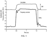
- figure 1 shows amplitude and frequency variation during a "010" modulation at 1Gb/s for a DML showing typical 6GHz adiabatic chirp.
- EMLs Externally Modulated Lasers
- the laser section of an EML remains at a constant injection current, thereby avoiding any adiabatic chirp, as illustrated Figure 2 , which shows amplitude (201) and frequency (203) variation during a "010" modulation at 1Gb/s for an EML (no adiabatic chirp).
- a DML can be operated with a low extinction ratio of about 3dB for example in order to limit the laser current variations.
- a filter can be added after the DML, such as for example a ring, or a Fabry-Perot etalon.
- a filter edge is positioned in order to pass the wavelength of 1-bits and attenuate the wavelength of 0-bits.
- This Frequency Modulation to Amplitude Modulation (FM-AM) conversion enables an increase in the extinction ratio to a high value (>6dB), while maintaining moderate chirp, reaching distances up to 80km at 10Gb/s for example.
- a chirp managed laser which is based on a DML with a selective filter, but with the additional feature that adiabatic chirp is half the bit rate, i.e. 5GHz for 10Gb/s (100ps-long bits) can be used.
- 1-bits interfere destructively with 0-bits. Transmission up to 200km at 10Gb/s has been demonstrated.
- phase shift section current I phase controls the position of emission wavelength I emission inside the laser stop-band delimited by ⁇ - and ⁇ +: when increasing I phase , I emission shifts towards ⁇ -.
- the external Bragg sections electrodes I DFB are directly modulated to generate laser amplitude modulation. Due to adiabatic chirp, the laser stop-band edges ⁇ - and ⁇ + both shift to higher wavelengths during 0-bit generation. By applying a counter-modulation to I phase , I emission can be shifted to the left side of the stop-band during 0-bit generation. It is thus possible to maintain a stable wavelength for I emission , meaning suppression of the adiabatic chirp.
- FIG. 3 is a schematic representation of a laser apparatus according to an example.
- the laser apparatus comprises periodically structured active regions 305, 307, and a phase shift region 309 adjacent to the periodically structured active regions.
- a value of phase current, I phase depends on the length, L phase , of the phase section 309.
- the length of the phase section 309 can be 100 ⁇ m, which enables sufficient tuning efficiency without increasing the cavity length too much.
- Dn phase ⁇ 0.01nm
- Both (external) facets (301, 303) of the periodically structured active regions 305, 307 are antireflection (AR) coated.
- the periodically structured active regions 305, 307 are DFB section gratings. These generate a stop-band between ⁇ - and ⁇ +, and when injecting current into the DFB sections (I DFB ) using a first driver 311, the laser apparatus lases at an emission wavelength ⁇ emission inside the stop-band of the apparatus. The position of ⁇ emission inside the stop-band depends on the phase condition of the central section 309. When injecting current (I phase ) into the phase section 309 using a second driver 313, the effective index of the phase section 309 decreases thereby changing the phase condition. Accordingly, ⁇ emission shifts towards lower wavelengths.
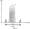
- Figure 4 is a schematic representation of a laser spectrum when varying I phase according to an example. As depicted, as the value of I phase is increased, ⁇ emission shifts towards lower wavelengths within the stop band (defined between ⁇ - and ⁇ +) of the laser apparatus. Thus, since chirp comes from a transition from 0 to 1 or 1 to 0, the effect can be minimised or removed using I phase .
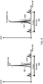
- FIG 5 is a schematic representation of a DFB spectrum for 0 and 1 bits according to an example.
- I DFB when modulating the external Bragg sections current I DFB (see figure 3 ), the whole emitted spectrum shifts between 0-bits (503) and 1-bits (501) due to adiabatic chirp (due to variations of n eff in the Bragg sections as described above).
- I phase is simultaneously increased during generation of a 0-bit
- the central peak 505 shifts towards the left-side of the stop-band, and can remain exactly aligned with 1-bit emission peak 507 by correctly choosing the I phase modulation amplitude. It is therefore possible to totally suppress the adiabatic chirp of the emitted wavelength using a counter-modulation of the phase section.
- Figure 6 is a schematic representation of a laser apparatus according to an example.
- the laser cavity of figure 3 is effectively folded on itself to provide one DFB section 601, a phase section 602 and a high-reflection (HR) coating 603 on the back facet 605.
- HR high-reflection
- FIG. 7 is a schematic representation of a transmitter according to an example.
- the transmitter 700 of figure 7 is suitable for use in a wireless telecommunications network 701.
- the transmitter comprises a laser structure 703, and a controller 705.
- the controller 705 is configured to select a first current for injection into a periodically structured active region of the laser structure 703 to generate an amplitude modulated optical output 707 of the transmitter 700, and select a counter-modulating current for injection into a phase shift region of the laser structure 703 to shift a wavelength of emission of the transmitter to stabilise the wavelength amplitude modulated optical output 707.
- the selected currents can be supplied (or injected) to the corresponding elements of the laser using appropriate drivers.
Landscapes
- Physics & Mathematics (AREA)
- Electromagnetism (AREA)
- Nonlinear Science (AREA)
- Engineering & Computer Science (AREA)
- Computer Networks & Wireless Communication (AREA)
- Signal Processing (AREA)
- Condensed Matter Physics & Semiconductors (AREA)
- General Physics & Mathematics (AREA)
- Optics & Photonics (AREA)
- Semiconductor Lasers (AREA)
Abstract
Description
- Aspects relate, in general, to a laser apparatus, a method and a transmitter.
- Directly modulated Lasers (DMLs), based on Distributed Feedback Lasers (DFBs) are widely used transmitters owing to their simple fabrication, simple control, and high output power. Output light amplitude is directly modulated by changing the laser current between a value close to threshold for 0-bits, and a value with high power for the 1-bits.
- According to an example, there is provided a laser apparatus comprising a periodically structured active region, a phase shift region adjacent to the periodically structured active region, a coating adjacent to the periodically structured active region, a first driver to inject a current into the periodically structured active region to generate an amplitude modulated optical output, and a second driver to inject a counter-modulating current into the phase shift region to shift a wavelength of emission of the laser apparatus. The periodically structured active region can be a diffraction grating. The coating can be an anti-reflective coating. A highly reflective coating can be provided adjacent the phase shift region. A second periodically structured active region adjacent to the phase shift region, and a second coating adjacent to the second periodically structured active region can be provided. The second coating can be an anti-reflective coating.
- According to an example, there is provided a method for supressing adiabatic chirp in the emission wavelength of a laser apparatus, the method comprising injecting a modulated current into a periodically structured active region of the laser apparatus to drive generation of an amplitude modulated optical output, and injecting a counter-modulating current into a phase shift region of the laser apparatus to shift the wavelength of emission of the optical output. The method can further comprise determining a level of adiabatic chirp as a result of a shift in laser apparatus stop-band due to a refractive index change stemming from generation of the amplitude modulated optical output, and selecting the counter-modulating current to supress the said adiabatic chirp by shifting the wavelength of emission of the optical output inside the stop-band. The adiabatic chirp can result from a transition of an optical output from or to a 0-bit. The method can further comprise injecting a counter-modulating current into a phase shift region of the laser apparatus to shift the wavelength of emission of the optical output towards the lower limit of the laser apparatus stop-band. The counter-modulating current can be selected to reduce the wavelength of emission of the optical output. The counter-modulating current can be between 2-20mA.
- According to an example, there is provided a transmitter for use in a wireless telecommunications network, the transmitter comprising a laser structure, and a controller to select a first current for injection into a periodically structured active region of the laser structure to generate an amplitude modulated optical output of the transmitter, and select a counter-modulating current for injection into a phase shift region of the laser structure to shift a wavelength of emission of the transmitter to stabilise the wavelength amplitude modulated optical output. The laser structure can comprise a coating adjacent to the periodically structured active region. The transmitter can further comprise a first driver to supply the first current into the periodically structured active region of the laser structure, and a second driver to supply the counter-modulating current into the phase shift region of the laser structure.
- Embodiments will now be described, by way of example only, with reference to the accompanying drawings, in which:
-
Figure 1 is a schematic representation of amplitude and frequency variation during a "010" modulation at 1Gb/s for a DML showing typical 6GHz adiabatic chirp; -
Figure 2 is a schematic representation of amplitude and frequency variation during a "010" modulation at 1Gb/s for an EML (no adiabatic chirp); -
Figure 3 is a schematic representation of a laser apparatus according to an example; -
Figure 4 is a schematic representation of a laser spectrum when varying Iphase according to an example; -
Figures 5a and 5b are schematic representations of a DFB spectrum for 0 and 1 bits according to an example; -
Figure 6 is a schematic representation of a laser apparatus according to an example; and -
Figure 7 is a schematic representation of a transmitter according to an example. - Example embodiments are described below in sufficient detail to enable those of ordinary skill in the art to embody and implement the systems and processes herein described. It is important to understand that embodiments can be provided in many alternate forms and should not be construed as limited to the examples set forth herein.
- Accordingly, while embodiments can be modified in various ways and take on various alternative forms, specific embodiments thereof are shown in the drawings and described in detail below as examples. There is no intent to limit to the particular forms disclosed. On the contrary, all modifications, equivalents, and alternatives falling within the scope of the appended claims should be included. Elements of the example embodiments are consistently denoted by the same reference numerals throughout the drawings and detailed description where appropriate.
- The terminology used herein to describe embodiments is not intended to limit the scope. The articles "a," "an," and "the" are singular in that they have a single referent, however the use of the singular form in the present document should not preclude the presence of more than one referent. In other words, elements referred to in the singular can number one or more, unless the context clearly indicates otherwise. It will be further understood that the terms "comprises," "comprising," "includes," and/or "including," when used herein, specify the presence of stated features, items, steps, operations, elements, and/or components, but do not preclude the presence or addition of one or more other features, items, steps, operations, elements, components, and/or groups thereof.
- Unless otherwise defined, all terms (including technical and scientific terms) used herein are to be interpreted as is customary in the art. It will be further understood that terms in common usage should also be interpreted as is customary in the relevant art and not in an idealized or overly formal sense unless expressly so defined herein.
- DMLs suffer from adiabatic chirp which limits transmission distance / bit rate. Output light amplitude is directly modulated by changing the laser current between a value close to threshold (I0) for 0-bits, and a value with high power (I1, typically 100mA for example) for the 1-bits. Changing the current generates a variation of carrier density in the laser cavity due to gain compression, leading to a variation of effective refractive index, neff. As the emitted wavelength of a DFB is given by λ = 2.neff.L, with L being the grating pitch, the variation of neff generates a variation of λ.
- Carrier density increases during generation of a 1-bit, leading to a lower neff by way of the plasma effect. That is, the wavelength decreases during generation of a 1-bit compared to a 0-bit by about 40 to 80nm, or in other words the optical frequency v = c / λ (c=speed of light) increases during 1-bit generation by 5 to 10GHz. This is illustrated schematically in
figure 1 , which shows amplitude and frequency variation during a "010" modulation at 1Gb/s for a DML showing typical 6GHz adiabatic chirp. - At 1.3µm transmissions (O-band), the effect is less detrimental due to low fibre chromatic dispersion, which is why DMLs are often preferred in this band. Still, transmission distances remain limited to about 20km at 25Gb/s for wavelengths on the edge of the O-band, which is a limitation for 100Gb ethernet based on 4x25Gb/s. At 1.55µm transmissions (C-band), the larger fibres dispersion (∼17ps/nm.km) drastically limits transmission to typically 10km at 10Gb/s, and 2km at 25Gb/s.
- To extend transmission distances Externally Modulated Lasers (EMLs) consisting of a laser section integrated with an electro-absorption modulator can be used. Contrary to DML structures, the laser section of an EML remains at a constant injection current, thereby avoiding any adiabatic chirp, as illustrated
Figure 2 , which shows amplitude (201) and frequency (203) variation during a "010" modulation at 1Gb/s for an EML (no adiabatic chirp). - However, these devices are more expensive, more power consuming, and provide a lower output power. Besides which, they are not compatible with uncooled operation due to the electro-absorption modulator's strong dependence on temperature.
- In order to reduce adiabatic chirp, a DML can be operated with a low extinction ratio of about 3dB for example in order to limit the laser current variations. A filter can be added after the DML, such as for example a ring, or a Fabry-Perot etalon. A filter edge is positioned in order to pass the wavelength of 1-bits and attenuate the wavelength of 0-bits. This Frequency Modulation to Amplitude Modulation (FM-AM) conversion enables an increase in the extinction ratio to a high value (>6dB), while maintaining moderate chirp, reaching distances up to 80km at 10Gb/s for example.
- To reach even longer distances, a chirp managed laser (CML), which is based on a DML with a selective filter, but with the additional feature that adiabatic chirp is half the bit rate, i.e. 5GHz for 10Gb/s (100ps-long bits) can be used. In this configuration, phase shift during a 0-bit is 2π x 5GHz x 100ps = π. Thus, after propagation, 1-bits interfere destructively with 0-bits. Transmission up to 200km at 10Gb/s has been demonstrated.
- However, such systems require the integration of a transmission filter which complicates laser assembly packaging and creates losses. They also impose a requirement for accurate control of detuning between laser and filter, and are not compatible with burst-mode operation of lasers.
- According to an example, there is provided a three-section phase-shift DFB laser with two external Bragg sections electrically connected together, and a central phase shift section controllable by an electrode. The phase shift section current Iphase controls the position of emission wavelength Iemission inside the laser stop-band delimited by λ- and λ+: when increasing Iphase, Iemission shifts towards λ-.
- In an example, the external Bragg sections electrodes IDFB are directly modulated to generate laser amplitude modulation. Due to adiabatic chirp, the laser stop-band edges λ- and λ+ both shift to higher wavelengths during 0-bit generation. By applying a counter-modulation to Iphase, Iemission can be shifted to the left side of the stop-band during 0-bit generation. It is thus possible to maintain a stable wavelength for Iemission, meaning suppression of the adiabatic chirp.
-
Figure 3 is a schematic representation of a laser apparatus according to an example. The laser apparatus comprises periodically structuredactive regions phase shift region 309 adjacent to the periodically structured active regions. - According to an example, a value of phase current, Iphase, forming the counter-modulation depends on the length, Lphase, of the
phase section 309. In the example offigure 3 , the length of thephase section 309 can be 100µm, which enables sufficient tuning efficiency without increasing the cavity length too much. Phase variation is:
- For a laser cavity total length of about 500µm (400µm of grating sections + 100µm phase section) the wavelength separation between cavity modes is the free spectral range, FSR = λ 2/2.ng.Lcavity (ng the group index, which is typically around ∼3.9 for example), therefore giving:

- So, a phase shift of π would lead to a tuning of 0.6nm.
- Supposing, in an example, an adiabatic chirp of 10GHz (which is a pessimistic evaluation), this corresponds to 0.08nm. So, to compensate for this chirp, a phase shift of π.(0.08)/(0.6) = 0.13.π can be used.
- This means 2.π.Dnphase.100µm / 1.55µm = 0.13.π, which means that Dnphase = 0.13 x 1.55µm / (2 x 100µm) = ∼0.001.
- In tuneable lasers such as DBR lasers, a value of Dn phase = ∼0.01nm can be obtained with 40mA over a 100µm-long passive Bragg section (not linear, Dn phase goes with 1^3). So, even if the phase section is optimised for tuning as in a tuneable laser, the current will be around 3mA. If the phase section is only a passive material (such as the modulator stack), 10mA should still be sufficient.
- Both (external) facets (301, 303) of the periodically structured
active regions figure 3 , the periodically structuredactive regions first driver 311, the laser apparatus lases at an emission wavelength λemission inside the stop-band of the apparatus. The position of λemission inside the stop-band depends on the phase condition of thecentral section 309. When injecting current (Iphase) into thephase section 309 using asecond driver 313, the effective index of thephase section 309 decreases thereby changing the phase condition. Accordingly, λemission shifts towards lower wavelengths. -
Figure 4 is a schematic representation of a laser spectrum when varying Iphase according to an example. As depicted, as the value of Iphase is increased, λemission shifts towards lower wavelengths within the stop band (defined between λ- and λ+) of the laser apparatus. Thus, since chirp comes from a transition from 0 to 1 or 1 to 0, the effect can be minimised or removed using Iphase. -
Figure 5 is a schematic representation of a DFB spectrum for 0 and 1 bits according to an example. Infigure 5a , when modulating the external Bragg sections current IDFB (seefigure 3 ), the whole emitted spectrum shifts between 0-bits (503) and 1-bits (501) due to adiabatic chirp (due to variations of neff in the Bragg sections as described above). Referring tofigure 5b , if Iphase is simultaneously increased during generation of a 0-bit, thecentral peak 505 shifts towards the left-side of the stop-band, and can remain exactly aligned with 1-bit emission peak 507 by correctly choosing the Iphase modulation amplitude. It is therefore possible to totally suppress the adiabatic chirp of the emitted wavelength using a counter-modulation of the phase section. -
Figure 6 is a schematic representation of a laser apparatus according to an example. In the example offigure 6 , the laser cavity offigure 3 is effectively folded on itself to provide oneDFB section 601, aphase section 602 and a high-reflection (HR) coating 603 on theback facet 605. -
Figure 7 is a schematic representation of a transmitter according to an example. Thetransmitter 700 offigure 7 is suitable for use in awireless telecommunications network 701. The transmitter comprises alaser structure 703, and acontroller 705. Thecontroller 705 is configured to select a first current for injection into a periodically structured active region of thelaser structure 703 to generate an amplitude modulatedoptical output 707 of thetransmitter 700, and select a counter-modulating current for injection into a phase shift region of thelaser structure 703 to shift a wavelength of emission of the transmitter to stabilise the wavelength amplitude modulatedoptical output 707. The selected currents can be supplied (or injected) to the corresponding elements of the laser using appropriate drivers. - The present inventions can be embodied in other specific apparatus and/or methods. The described embodiments are to be considered in all respects as illustrative and not restrictive. In particular, the scope of the invention is indicated by the appended claims rather than by the description and figures herein. All changes that come within the meaning and range of equivalency of the claims are to be embraced within their scope.
Claims (15)
- A laser apparatus comprising:a periodically structured active region;a phase shift region adjacent to the periodically structured active region;a coating adjacent to the periodically structured active region;a first driver to inject a current into the periodically structured active region to generate an amplitude modulated optical output; anda second driver to inject a counter-modulating current into the phase shift region to shift a wavelength of emission of the laser apparatus.
- The laser apparatus as claimed in claim 1, wherein the periodically structured active region is a diffraction grating.
- The laser apparatus as claimed in claim 1 or 2, wherein the coating is an anti-reflective coating.
- The laser apparatus as claimed in any preceding claim, further comprising a highly reflective coating adjacent the phase shift region.
- The laser apparatus as claimed in any of claims 1 to 3, further comprising a second periodically structured active region adjacent to the phase shift region; and
a second coating adjacent to the second periodically structured active region. - The laser apparatus as claimed in claim 5, wherein the second coating is an anti-reflective coating.
- A method for supressing adiabatic chirp in the emission wavelength of a laser apparatus, the method comprising:injecting a modulated current into a periodically structured active region of the laser apparatus to drive generation of an amplitude modulated optical output; andinjecting a counter-modulating current into a phase shift region of the laser apparatus to shift the wavelength of emission of the optical output.
- The method as claimed in claim 7, further comprising:determining a level of adiabatic chirp as a result of a shift in laser apparatus stop-band due to a refractive index change stemming from generation of the amplitude modulated optical output; andselecting the counter-modulating current to supress the said adiabatic chirp by shifting the wavelength of emission of the optical output inside the stop-band.
- The method as claimed in claim 7 or 8, wherein the adiabatic chirp results from transition of an optical output from or to a 0-bit.
- The method as claimed in claim 8, further comprising:injecting a counter-modulating current into a phase shift region of the laser apparatus to shift the wavelength of emission of the optical output towards the lower limit of the laser apparatus stop-band.
- The method as claimed in any of claims 7 to 10, wherein the counter-modulating current is selected to reduce the wavelength of emission of the optical output.
- The method as claimed in any of claims 7 to 11, wherein the counter-modulating current is between 2-20mA.
- A transmitter for use in a wireless telecommunications network, the transmitter comprising:a laser structure; anda controller to:select a first current for injection into a periodically structured active region of the laser structure to generate an amplitude modulated optical output of the transmitter; andselect a counter-modulating current for injection into a phase shift region of the laser structure to shift a wavelength of emission of the transmitter to stabilise the wavelength amplitude modulated optical output.
- The transmitter as claimed in claim 13, wherein the laser structure comprises a coating adjacent to the periodically structured active region.
- The transmitter as claimed in claim 13 or 14, further comprising:a first driver to supply the first current into the periodically structured active region of the laser structure; anda second driver to supply the counter-modulating current into the phase shift region of the laser structure.
Priority Applications (1)
| Application Number | Priority Date | Filing Date | Title |
|---|---|---|---|
| EP19305006.9A EP3678307A1 (en) | 2019-01-03 | 2019-01-03 | Laser apparatus |
Applications Claiming Priority (1)
| Application Number | Priority Date | Filing Date | Title |
|---|---|---|---|
| EP19305006.9A EP3678307A1 (en) | 2019-01-03 | 2019-01-03 | Laser apparatus |
Publications (1)
| Publication Number | Publication Date |
|---|---|
| EP3678307A1 true EP3678307A1 (en) | 2020-07-08 |
Family
ID=65228479
Family Applications (1)
| Application Number | Title | Priority Date | Filing Date |
|---|---|---|---|
| EP19305006.9A Withdrawn EP3678307A1 (en) | 2019-01-03 | 2019-01-03 | Laser apparatus |
Country Status (1)
| Country | Link |
|---|---|
| EP (1) | EP3678307A1 (en) |
Cited By (1)
| Publication number | Priority date | Publication date | Assignee | Title |
|---|---|---|---|---|
| US12609718B2 (en) | 2023-06-14 | 2026-04-21 | Hewlett Packard Enterprise Development Lp | WiFi-7 optimized split band architecture and method of operation |
Citations (4)
| Publication number | Priority date | Publication date | Assignee | Title |
|---|---|---|---|---|
| US5119393A (en) * | 1989-06-14 | 1992-06-02 | Hitachi, Ltd. | Semiconductor laser device capable of controlling wavelength shift |
| US20040036943A1 (en) * | 2002-08-22 | 2004-02-26 | Freund Joseph Michael | Electroabsorption modulator with tunable chirp |
| US7564889B2 (en) * | 2002-11-06 | 2009-07-21 | Finisar Corporation | Adiabatically frequency modulated source |
| US20130308178A1 (en) * | 2012-05-17 | 2013-11-21 | Finisar Corporation | Co-modulation of DBR Laser and Integrated Optical Amplifier |
-
2019
- 2019-01-03 EP EP19305006.9A patent/EP3678307A1/en not_active Withdrawn
Patent Citations (4)
| Publication number | Priority date | Publication date | Assignee | Title |
|---|---|---|---|---|
| US5119393A (en) * | 1989-06-14 | 1992-06-02 | Hitachi, Ltd. | Semiconductor laser device capable of controlling wavelength shift |
| US20040036943A1 (en) * | 2002-08-22 | 2004-02-26 | Freund Joseph Michael | Electroabsorption modulator with tunable chirp |
| US7564889B2 (en) * | 2002-11-06 | 2009-07-21 | Finisar Corporation | Adiabatically frequency modulated source |
| US20130308178A1 (en) * | 2012-05-17 | 2013-11-21 | Finisar Corporation | Co-modulation of DBR Laser and Integrated Optical Amplifier |
Non-Patent Citations (2)
| Title |
|---|
| TROPPENZ U ET AL: "40 Gbit/s directly modulated lasers: physics and application", NOVEL IN-PLANE SEMICONDUCTOR LASERS X, SPIE, 1000 20TH ST. BELLINGHAM WA 98225-6705 USA, vol. 7953, no. 1, 10 February 2011 (2011-02-10), pages 1 - 10, XP060005542, [retrieved on 20110216], DOI: 10.1117/12.876137 * |
| ZHAO HANG ET AL: "Chirp-Compensated DBR Lasers for TWDM-PON Applications", IEEE PHOTONICS JOURNAL, IEEE, USA, vol. 7, no. 1, 1 February 2015 (2015-02-01), pages 1 - 9, XP011573345, [retrieved on 20150212], DOI: 10.1109/JPHOT.2015.2392377 * |
Cited By (1)
| Publication number | Priority date | Publication date | Assignee | Title |
|---|---|---|---|---|
| US12609718B2 (en) | 2023-06-14 | 2026-04-21 | Hewlett Packard Enterprise Development Lp | WiFi-7 optimized split band architecture and method of operation |
Similar Documents
| Publication | Publication Date | Title |
|---|---|---|
| Nakahara et al. | Direct modulation at 56 and 50 Gb/s of 1.3-$\mu $ m InGaAlAs ridge-shaped-BH DFB lasers | |
| Kreissl et al. | Up to 40 Gb/s directly modulated laser operating at low driving current: Buried-heterostructure passive feedback laser (BH-PFL) | |
| US20050053112A1 (en) | Surface emitting dfb laser structures for broadband communication systems and array of same | |
| EP3869640A1 (en) | Semiconductor laser, optical emission component, optical line terminal and optical network unit | |
| US9048618B2 (en) | Short gain cavity distributed bragg reflector laser | |
| CN106030937B (en) | Tunable laser device | |
| US20130094527A1 (en) | Wavelength monitor, wavelength lockable laser diode and method for locking emission wavelength of laser diode | |
| CA2526124A1 (en) | Q-modulated semiconductor laser | |
| Yamamoto | High-speed directly modulated lasers | |
| Tadokoro et al. | 43 Gb/s 1.3 μm DFB laser for 40 km transmission | |
| EP1454393B1 (en) | Phase shifted surface emitting dfb laser structures with gain or absorptive gratings | |
| US20040258119A1 (en) | Method and apparatus for suppression of spatial-hole burning in second of higher order DFB lasers | |
| JP4905854B2 (en) | Direct modulation tunable laser | |
| Kudo et al. | 1.52-1.59-μm range different-wavelength modulator-integrated DFB-LDs fabricated on a single wafer | |
| Usami et al. | Suppression of longitudinal spatial hole-burning effect in lambda/4-shifted DFB lasers by nonuniform current distribution | |
| EP3678307A1 (en) | Laser apparatus | |
| JP7107180B2 (en) | Multi-wavelength optical transmitter | |
| CN115441305A (en) | DFB+R laser structure for directly modulated laser | |
| EP3518357B1 (en) | Laser with full c-band tunability and narrow linewidth | |
| JP7502684B2 (en) | Tunable Optical Transmitter | |
| Debrégeas | Widely tunable laser diodes | |
| Okai et al. | Complex-coupled/spl lambda//4-shifted DFB lasers with a flat FM response | |
| GB2437593A (en) | A q-modulated semiconductor laser | |
| Kano et al. | Characteristics of super structure grating (SSG) DBR lasers under broad range wavelength tuning | |
| Takaki et al. | High-power CW-DFB LDs for optical communications |
Legal Events
| Date | Code | Title | Description |
|---|---|---|---|
| PUAI | Public reference made under article 153(3) epc to a published international application that has entered the european phase |
Free format text: ORIGINAL CODE: 0009012 |
|
| STAA | Information on the status of an ep patent application or granted ep patent |
Free format text: STATUS: THE APPLICATION HAS BEEN PUBLISHED |
|
| AK | Designated contracting states |
Kind code of ref document: A1 Designated state(s): AL AT BE BG CH CY CZ DE DK EE ES FI FR GB GR HR HU IE IS IT LI LT LU LV MC MK MT NL NO PL PT RO RS SE SI SK SM TR |
|
| AX | Request for extension of the european patent |
Extension state: BA ME |
|
| STAA | Information on the status of an ep patent application or granted ep patent |
Free format text: STATUS: REQUEST FOR EXAMINATION WAS MADE |
|
| 17P | Request for examination filed |
Effective date: 20201221 |
|
| RBV | Designated contracting states (corrected) |
Designated state(s): AL AT BE BG CH CY CZ DE DK EE ES FI FR GB GR HR HU IE IS IT LI LT LU LV MC MK MT NL NO PL PT RO RS SE SI SK SM TR |
|
| STAA | Information on the status of an ep patent application or granted ep patent |
Free format text: STATUS: EXAMINATION IS IN PROGRESS |
|
| 17Q | First examination report despatched |
Effective date: 20220510 |
|
| STAA | Information on the status of an ep patent application or granted ep patent |
Free format text: STATUS: THE APPLICATION IS DEEMED TO BE WITHDRAWN |
|
| 18D | Application deemed to be withdrawn |
Effective date: 20250916 |