EP3678292A1 - Magnetically pumped voltage controlled oscillator - Google Patents
Magnetically pumped voltage controlled oscillator Download PDFInfo
- Publication number
- EP3678292A1 EP3678292A1 EP19210414.9A EP19210414A EP3678292A1 EP 3678292 A1 EP3678292 A1 EP 3678292A1 EP 19210414 A EP19210414 A EP 19210414A EP 3678292 A1 EP3678292 A1 EP 3678292A1
- Authority
- EP
- European Patent Office
- Prior art keywords
- inductor
- coupled
- node
- transistor
- tank circuit
- Prior art date
- Legal status (The legal status is an assumption and is not a legal conclusion. Google has not performed a legal analysis and makes no representation as to the accuracy of the status listed.)
- Granted
Links
Images



Classifications
-
- H—ELECTRICITY
- H03—ELECTRONIC CIRCUITRY
- H03B—GENERATION OF OSCILLATIONS, DIRECTLY OR BY FREQUENCY-CHANGING, BY CIRCUITS EMPLOYING ACTIVE ELEMENTS WHICH OPERATE IN A NON-SWITCHING MANNER; GENERATION OF NOISE BY SUCH CIRCUITS
- H03B5/00—Generation of oscillations using amplifier with regenerative feedback from output to input
- H03B5/08—Generation of oscillations using amplifier with regenerative feedback from output to input with frequency-determining element comprising lumped inductance and capacitance
- H03B5/12—Generation of oscillations using amplifier with regenerative feedback from output to input with frequency-determining element comprising lumped inductance and capacitance active element in amplifier being semiconductor device
- H03B5/1228—Generation of oscillations using amplifier with regenerative feedback from output to input with frequency-determining element comprising lumped inductance and capacitance active element in amplifier being semiconductor device the amplifier comprising one or more field effect transistors
-
- H—ELECTRICITY
- H03—ELECTRONIC CIRCUITRY
- H03B—GENERATION OF OSCILLATIONS, DIRECTLY OR BY FREQUENCY-CHANGING, BY CIRCUITS EMPLOYING ACTIVE ELEMENTS WHICH OPERATE IN A NON-SWITCHING MANNER; GENERATION OF NOISE BY SUCH CIRCUITS
- H03B5/00—Generation of oscillations using amplifier with regenerative feedback from output to input
- H03B5/08—Generation of oscillations using amplifier with regenerative feedback from output to input with frequency-determining element comprising lumped inductance and capacitance
- H03B5/12—Generation of oscillations using amplifier with regenerative feedback from output to input with frequency-determining element comprising lumped inductance and capacitance active element in amplifier being semiconductor device
- H03B5/1206—Generation of oscillations using amplifier with regenerative feedback from output to input with frequency-determining element comprising lumped inductance and capacitance active element in amplifier being semiconductor device using multiple transistors for amplification
- H03B5/1212—Generation of oscillations using amplifier with regenerative feedback from output to input with frequency-determining element comprising lumped inductance and capacitance active element in amplifier being semiconductor device using multiple transistors for amplification the amplifier comprising a pair of transistors, wherein an output terminal of each being connected to an input terminal of the other, e.g. a cross coupled pair
-
- H—ELECTRICITY
- H03—ELECTRONIC CIRCUITRY
- H03B—GENERATION OF OSCILLATIONS, DIRECTLY OR BY FREQUENCY-CHANGING, BY CIRCUITS EMPLOYING ACTIVE ELEMENTS WHICH OPERATE IN A NON-SWITCHING MANNER; GENERATION OF NOISE BY SUCH CIRCUITS
- H03B5/00—Generation of oscillations using amplifier with regenerative feedback from output to input
- H03B5/08—Generation of oscillations using amplifier with regenerative feedback from output to input with frequency-determining element comprising lumped inductance and capacitance
- H03B5/12—Generation of oscillations using amplifier with regenerative feedback from output to input with frequency-determining element comprising lumped inductance and capacitance active element in amplifier being semiconductor device
- H03B5/1206—Generation of oscillations using amplifier with regenerative feedback from output to input with frequency-determining element comprising lumped inductance and capacitance active element in amplifier being semiconductor device using multiple transistors for amplification
- H03B5/1218—Generation of oscillations using amplifier with regenerative feedback from output to input with frequency-determining element comprising lumped inductance and capacitance active element in amplifier being semiconductor device using multiple transistors for amplification the generator being of the balanced type
-
- H—ELECTRICITY
- H03—ELECTRONIC CIRCUITRY
- H03B—GENERATION OF OSCILLATIONS, DIRECTLY OR BY FREQUENCY-CHANGING, BY CIRCUITS EMPLOYING ACTIVE ELEMENTS WHICH OPERATE IN A NON-SWITCHING MANNER; GENERATION OF NOISE BY SUCH CIRCUITS
- H03B5/00—Generation of oscillations using amplifier with regenerative feedback from output to input
- H03B5/08—Generation of oscillations using amplifier with regenerative feedback from output to input with frequency-determining element comprising lumped inductance and capacitance
- H03B5/12—Generation of oscillations using amplifier with regenerative feedback from output to input with frequency-determining element comprising lumped inductance and capacitance active element in amplifier being semiconductor device
- H03B5/1231—Generation of oscillations using amplifier with regenerative feedback from output to input with frequency-determining element comprising lumped inductance and capacitance active element in amplifier being semiconductor device the amplifier comprising one or more bipolar transistors
-
- H—ELECTRICITY
- H03—ELECTRONIC CIRCUITRY
- H03B—GENERATION OF OSCILLATIONS, DIRECTLY OR BY FREQUENCY-CHANGING, BY CIRCUITS EMPLOYING ACTIVE ELEMENTS WHICH OPERATE IN A NON-SWITCHING MANNER; GENERATION OF NOISE BY SUCH CIRCUITS
- H03B5/00—Generation of oscillations using amplifier with regenerative feedback from output to input
- H03B5/08—Generation of oscillations using amplifier with regenerative feedback from output to input with frequency-determining element comprising lumped inductance and capacitance
- H03B5/12—Generation of oscillations using amplifier with regenerative feedback from output to input with frequency-determining element comprising lumped inductance and capacitance active element in amplifier being semiconductor device
- H03B5/1296—Generation of oscillations using amplifier with regenerative feedback from output to input with frequency-determining element comprising lumped inductance and capacitance active element in amplifier being semiconductor device the feedback circuit comprising a transformer
-
- H—ELECTRICITY
- H03—ELECTRONIC CIRCUITRY
- H03L—AUTOMATIC CONTROL, STARTING, SYNCHRONISATION OR STABILISATION OF GENERATORS OF ELECTRONIC OSCILLATIONS OR PULSES
- H03L7/00—Automatic control of frequency or phase; Synchronisation
- H03L7/06—Automatic control of frequency or phase; Synchronisation using a reference signal applied to a frequency- or phase-locked loop
- H03L7/08—Details of the phase-locked loop
- H03L7/099—Details of the phase-locked loop concerning mainly the controlled oscillator of the loop
Definitions
- the present invention relates to an oscillator circuit, and more particularly, to a magnetically pumped voltage controlled oscillator.
- a voltage controlled oscillator is an oscillator circuit that outputs an oscillating signal having a frequency that varies in response to an input control voltage.
- VCOs are fundamental components that are employed in a broad range of applications.
- VCOs are utilized for phase locked loop (PLL) circuits.
- a conventional VCO may employ an inductor-capacitor (LC) tank to act as a resonator.
- LC inductor-capacitor
- MOS metal oxide semiconductor
- One of the objectives of the claimed invention is to provide a magnetically pumped voltage controlled oscillator.
- an exemplary voltage controlled oscillator includes a first inductor, a second inductor, a first metal oxide semiconductor (MOS) transistor, a second MOS transistor, and an inductor-capacitor (LC) tank circuit.
- a first end of the first inductor and a first end of the second inductor are both coupled to a first power rail.
- a drain node of the first MOS transistor is coupled to the second end of the first inductor, and a source node of the first MOS transistor is coupled to a second power rail.
- a drain node of the second MOS transistor is coupled to the second end of the second inductor, and a source node of the second MOS transistor is coupled to the second power rail.
- the LC tank circuit is coupled to the gate node of the first MOS transistor and the gate node of the second MOS transistor, wherein energy is magnetically pumped into the LC tank circuit through the first inductor and the second inductor, such that there is no direct connection between the LC tank circuit and the drain node of the first MOS transistor and there is no direct connection between the LC tank circuit and the drain node of the second MOS transistor.
- an exemplary voltage controlled oscillator includes a first inductor, a second inductor, a first P-channel metal oxide semiconductor (PMOS) transistor, a second PMOS transistor, a first N-channel metal oxide semiconductor (NMOS) transistor, a second NMOS transistor, and an inductor-capacitor (LC) tank circuit.
- a first end of the second inductor is coupled to a first end of the first inductor.
- a drain node of the first PMOS transistor is coupled to a second end of the first inductor, and a source node of the first MOS transistor is coupled to a first power rail.
- a drain node of the second PMOS transistor is coupled to a second end of the second inductor, and a source node of the second PMOS transistor is coupled to the first power rail.
- a drain node of the first NMOS transistor is coupled to the second end of the first inductor, and a source node of the first MOS transistor is coupled to a second power rail.
- a drain node of the second NMOS transistor is coupled to the second end of the second inductor, and a source node of the second NMOS transistor is coupled to the second power rail.
- the LC tank circuit is coupled to the gate node of the first PMOS transistor, the gate node of the second PMOS transistor, the gate node of the first NMOS transistor, and the gate node of the second NMOS transistor, wherein energy is magnetically pumped into the LC tank circuit through the first inductor and the second inductor, such that there is no direct connection between the LC tank circuit and the drain node of each of the first PMOS transistor and the first NMOS transistor and there is no direct connection between the LC tank circuit and the drain node of each of the second PMOS transistor and the second NMOS transistor.
- an exemplary voltage controlled oscillator includes a first inductor, a second inductor, a third inductor, a fourth inductor, a first P-channel metal oxide semiconductor (PMOS) transistor, a second PMOS transistor, a first N-channel metal oxide semiconductor (NMOS) transistor, a second NMOS transistor, and an inductor-capacitor (LC) tank circuit.
- a first end of the second inductor is coupled to a first end of the first inductor.
- a first end of the fourth inductor is coupled to a first end of the third inductor.
- a drain node of the first PMOS transistor is coupled to a second end of the first inductor, and a source node of the first MOS transistor is coupled to a first power rail.
- a drain node of the second PMOS transistor is coupled to a second end of the second inductor, and a source node of the second PMOS transistor is coupled to the first power rail.
- a drain node of the first NMOS transistor is coupled to a second end of the third inductor, and a source node of the first MOS transistor is coupled to a second power rail.
- a drain node of the second NMOS transistor is coupled to a second end of the fourth inductor, and a source node of the second NMOS transistor is coupled to the second power rail.
- the LC tank circuit is coupled to the gate node of the first PMOS transistor, the gate node of the second PMOS transistor, the gate node of the first NMOS transistor, and the gate node of the second NMOS transistor, wherein energy is magnetically pumped into the LC tank circuit through the first inductor, the second inductor, the third inductor, and the fourth inductor, such that there is no direct connection between the LC tank circuit and the drain node of each of the first PMOS transistor and the first NMOS transistor and there is no direct connection between the LC tank circuit and the drain node of each of the second PMOS transistor and the second NMOS transistor.
- FIG. 1 is a circuit diagram illustrating a first magnetically pumped voltage controlled oscillator (VCO) according to an embodiment of the present invention.
- the VCO 100 includes a single inductor-capacitor (LC) tank circuit 102, a plurality of inductors L1 and L2, and a plurality of N-channel metal oxide semiconductor (NMOS) transistors MN1 and MN2.
- the LC tank circuit 102 includes a plurality of inductors L3 and L4 and a capacitor C.
- the capacitor C may be implemented by a voltage-controlled capacitor that is used to adjust a resonant frequency of the LC tank circuit 102 in response to a control voltage of the VCO.
- One end N11 of the inductor L1 is coupled to a power rail VDD, and the other end N12 of the inductor L1 is coupled to a drain node of the NMOS transistor MN1.
- One end N21 of the inductor L2 is coupled to the power rail VDD, and the other end N22 of the inductor L2 is coupled to a drain node of the NMOS transistor MN2.
- a source node of the NMOS transistor MN1 and a source node of the NMOS transistor MN2 are both coupled to a power rail GND.
- the power rail VDD is used to deliver a supply voltage (e.g., 0.6V or 0.8V)
- the power rail GND is used to deliver a ground voltage (e.g., 0V).
- the LC tank circuit 102 is coupled to a gate node of the NMOS transistor MN1 and a gate node of the NMOS transistor MN2.
- energy is magnetically pumped into the LC tank circuit 102 through the inductors L1 and L2, such that there is no direct connection between the LC tank circuit 102 and the drain node of the MOS transistor MN1 and there is no direct connection between the LC tank circuit 102 and the drain node of the MOS transistor MN2.
- the LC tank circuit 102 and the NMOS transistors MN1 and MN2 are cross-coupled.
- the LC tank circuit 102 is directly connected to gate nodes of the NMOS transistor MN1 and MN2 without via any magnetic coupling (i.e., inductive coupling). Hence, the pumping force is not weakened significantly due to the fact the LC tank circuit 102 is not totally separated from drain nodes and gate nodes of NMOS transistors MN1 and MN2.
- the inductor L3 is magnetically coupled to the inductor L1, where one end N31 of the inductor L3 is coupled to a bias voltage V G_BIAS_N that may be generated from a bias voltage generator (not shown), and the other end N32 of the inductor L3 is coupled to one end N51 of the capacitor C; and the inductor L4 is magnetically coupled to the inductor L2, where one end N41 of the inductor L4 is coupled to the bias voltage V G_BIAS_N , and the other end N42 of the inductor L4 is coupled to the other end N52 of the capacitor C.
- the inductors L1 and L2 may have the same inductance value L D
- the inductors L3 and L4 may have the same inductance value L G
- magnetic coupling i.e., inductive coupling
- inductors L1 and L3 and magnetic coupling i.e., inductive coupling
- inductors L2 and L4 may have the same coupling coefficient k.
- the non-linear capacitor C of the LC tank circuit 102 is not directly connected to drain nodes of the NMOS transistors MN1 and MN2.
- the non-linear capacitor issue at the drain nodes of the NMOS transistors MN1 and MN2 can be mitigated.
- the thermal noise introduced by NMOS transistors MN1 and MN2 is attenuated by the magnetic coupling (i.e., inductive coupling), such that only a fraction M L G of the thermal noise enters the LC tank circuit 102.
- the undesired noise conversion at the LC tank circuit 102 is effectively mitigated.
- the negative transconductance (-g m ) resulting from the cross-coupling configuration of the NMOS transistors MN1 and MN2 may also be reduced by the magnetic coupling (i.e., inductive coupling).
- the NMOS transistors MN1 and MN2 may be implemented by large-sized transistors. However, this is for illustrative purposes only, and is not meant to be a limitation of the present invention.
- a resonant frequency F OSC of the LC tank circuit 102 depends on the inductance value L G of the inductor L3/L4, and is independent of the inductance value L D of the inductor L1/L2 and the coupling coefficient k of magnetic coupling (i.e., inductive coupling).
- the quality factor Q of each inductor L3/L4 has the same requirement as the conventional VCO. Since the resonant frequency F OSC is independent of the inductance value L D , the quality factor Q of each inductor L1/L2 can be much more relaxed without affecting the oscillation result.
- a voltage swing at the gate node and a voltage swing at the drain node can be separately designed.
- L G and M A proper design of the parameters L G and M can ensure that there is a larger voltage swing at the LC tank circuit 102 (i.e., a large voltage swing at the gate node of each NMOS transistor MN1/MN2) and there is a smaller voltage swing at the drain node of each NMOS transistor MN1/MN2.
- the gate swing of the NMOS transistor MN1/MN2 is no longer limited by the rail voltages.
- the drain swing of the NMOS transistor MN1/MN2 can be minimized to achieve lower noise conversion at the LC tank circuit 102.
- the LC tank circuit 102 has additional loss and degrades the phase noise performance.
- a proper design can achieve larger gate swing and smaller drain swing (e.g., V PP _Gate > V PP _Drain).
- V PP _Gate > V PP _Drain
- the voltage swing at the gate node V PP _Gate and the voltage swing at the drain node V PP_ Drain may be properly designed to prevent any of the NMOS transistors MN1 and MN2 from entering the triode region.
- any of the NMOS transistors MN1 and MN2 is prevented from entering the triode region due to V PP _Gate > V PP _Drain.
- LC tank circuit 102 Since the LC tank circuit 102 is coupled to gate nodes of NMOS transistors MN1 and MN2 without being directly connected to drain nodes of NMOS transistors MN1 and MN2, biasing at gate nodes is not determined by voltages at drain nodes. Hence, the biasing at gate nodes of the VCO 100 can be freely adjusted for a power-efficient operation. In other words, a low-power magnetically pumped VCO is realized by individually setting the bias voltage V G_BIAS_N .
- MOS transistors employed by the VCO 100 are NMOS transistors.
- PMOS P-channel metal oxide semiconductor
- CMOS complementary metal oxide semiconductor
- each consisting of a PMOS transistor and an NMOS transistor may be employed by a magnetically pumped VCO.
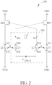
- FIG. 2 is a circuit diagram illustrating a second magnetically pumped VCO according to an embodiment of the present invention.
- the VCO 200 includes a single LC tank circuit 202, a plurality of inductors L1 and L2, and a plurality of PMOS transistors MP1 and MP2.
- the LC tank circuit 202 includes a plurality of inductors L3 and L4 and a capacitor C.
- the capacitor C may be implemented by a voltage-controlled capacitor that is used to adjust a resonant frequency of the LC tank circuit 202 in response to a control voltage of the VCO.
- One end N12 of the inductor L1 is coupled to a power rail GND, and the other end N11 of the inductor L1 is coupled to a drain node of the PMOS transistor MP1.
- One end N22 of the inductor L2 is coupled to the power rail GND, and the other end N21 of the inductor L2 is coupled to a drain node of the PMOS transistor MP2.
- a source node of the PMOS transistor MP1 and a source node of the PMOS transistor MP2 are both coupled to a power rail VDD.
- the power rail VDD is used to deliver a supply voltage (e.g., 0.6V or 0.8V)
- the power rail GND is used to deliver a ground voltage (e.g., 0V).
- the LC tank circuit 202 is coupled to a gate node of the PMOS transistor MP1 and a gate node of the PMOS transistor MP2.
- energy is magnetically pumped into the LC tank circuit 202 through the inductors L1 and L2, such that there is no direct connection between the LC tank circuit 202 and the drain node of the PMOS transistor MP1 and there is no direct connection between the LC tank circuit 202 and the drain node of the PMOS transistor MP2.
- the LC tank circuit 202 and the PMOS transistors MP1 and MP2 are cross-coupled.
- one end N51 of the capacitor C is coupled to a gate node of the PMOS transistor MP2, and the other end N52 of the capacitor C is coupled to a gate node of the PMOS transistor MP1 , where differential oscillating signals are generated at two ends of the capacitor C.
- the LC tank circuit 202 is directly connected to gate nodes of the PMOS transistor MP1 and MP2 without via any magnetic coupling (i.e., inductive coupling). Hence, the pumping force is not weakened significantly due to the fact the LC tank circuit 202 is not totally separated from drain nodes and gate nodes of PMOS transistors MP1 and MP2.
- the inductor L3 is magnetically coupled to the inductor L1, where one end N32 of the inductor L3 is coupled to a bias voltage V G_BIAS_P that may be generated from a bias voltage generator (not shown), and the other end N31 of the inductor L3 is coupled to one end N51 of the capacitor C; and the inductor L4 is magnetically coupled to the inductor L2, where one end N42 of the inductor L4 is coupled to the bias voltage V G_BIAS_P , and the other end N41 of the inductor L4 is coupled to the other end N52 of the capacitor C.
- the inductors L1 and L2 may have the same inductance value L D
- the inductors L3 and L4 may have the same inductance value L G
- magnetic coupling i.e., inductive coupling
- inductors L1 and L3 and magnetic coupling i.e., inductive coupling
- inductors L2 and L4 may have the same coupling coefficient k.
- the non-linear capacitor C of the LC tank circuit 202 is not directly connected to drain nodes of the PMOS transistors MP1 and MP2.
- the non-linear capacitor issue at the drain nodes of the PMOS transistors MP1 and MP2 can be mitigated.
- the thermal noise introduced by PMOS transistors MP1 and MP2 is attenuated by the magnetic coupling (i.e., inductive coupling), such that only a fraction M L G of the thermal noise enters the LC tank circuit 202.
- the undesired noise conversion at the LC tank circuit 202 is effectively mitigated.
- the negative transconductance (-g m ) resulting from the cross-coupling configuration of the PMOS transistors MP1 and MP2 may also be reduced by the magnetic coupling (i.e., inductive coupling).
- the PMOS transistors MP1 and MP2 may be implemented by large-sized transistors. However, this is for illustrative purposes only, and is not meant to be a limitation of the present invention.
- a resonant frequency F OSC of the LC tank circuit 202 depends on the inductance value L G of the inductor L3/L4, and is independent of the inductance value L D of the inductor L1/L2 and the coupling coefficient k of magnetic coupling (i.e., inductive coupling).
- the quality factor Q of each inductor L3/L4 has the same requirement as the conventional VCO. Since the resonant frequency F OSC is independent of the inductance value L D , the quality factor Q of each inductor L1/L2 can be much more relaxed without affecting the oscillation result.
- a voltage swing at the gate node and a voltage swing at the drain node can be separately designed.
- a proper design of the parameters L G and M can ensure that there is a larger voltage swing at the LC tank circuit 202 (i.e., a large voltage swing at the gate node of each PMOS transistor MP1/MP2) and there is a smaller voltage swing at the drain node of each PMOS transistor MP1/MP2.
- the gate swing of the PMOS transistor MP1/MP2 is no longer limited by the rail voltages. For example, V PP _Gate > 2*VDD. To put it simply, the gate swing of the PMOS transistor MP1/MP2 can be maximized. In addition, the drain swing of the PMOS transistor MP1/MP2 can be minimized to achieve lower noise conversion at the LC tank circuit 202.
- the LC tank circuit 202 has additional loss and degrades the phase noise performance.
- a proper design can achieve larger gate swing and smaller drain swing (e.g., V PP _Gate > V PP _Drain).
- V PP _Gate > V PP _Drain
- the voltage swing at the gate node V PP _Gate and the voltage swing at the drain node V PP_ Drain are properly designed to prevent any of the PMOS transistors MP1 and MP2 from entering the triode region.
- any of the PMOS transistors MP1 and MP2 is prevented from entering the triode region due to V PP _Gate > V PP _Drain.
- LC tank circuit 202 Since the LC tank circuit 202 is coupled to gate nodes of PMOS transistors MP1 and MP2 without being directly connected to drain nodes of PMOS transistors MP1 and MP2, biasing at gate nodes is not determined by voltages of drain nodes. Hence, the biasing at gate nodes of the VCO 200 can be freely adjusted for a power-efficient operation. In other words, a low-power magnetically pumped VCO is realized by individually setting the bias voltage V G_BIAS_P .
- FIG. 3 is a circuit diagram illustrating a third magnetically pumped VCO according to an embodiment of the present invention.
- the VCO 300 includes a single LC tank circuit 302, a plurality of inductors L1 and L2, a plurality of NMOS transistors MN1 and MN2, and a plurality of PMOS transistors MP1 and MP2.
- the LC tank circuit 302 includes a plurality of inductors L3 and L4 and a capacitor C.
- the capacitor C may be implemented by a voltage-controlled capacitor that is used to adjust a resonant frequency of the LC tank circuit 302 in response to a control voltage of the VCO.
- a drain end of the PMOS transistor MP1 and a drain end of the NMOS transistor MN1 are both coupled to one end N12 of the inductor L1.
- a drain end of the PMOS transistor MP2 and a drain end of the NMOS transistor MN2 are both coupled to one end N22 of the inductor L2.
- a source end of the PMOS transistor MP1 and a source end of the PMOS transistor MP2 are both coupled to a power rail VDD.
- a source end of the NMOS transistor MN1 and a source end of the NMOS transistor MN2 are both coupled to a power rail GND.
- the other end N11 of the inductor L1 is coupled to the other end N21 of the inductor L2, where a bias voltage V G _ BIAS applied to ends N11 and N21 of inductors L1 and L2 may be generated from a bias voltage generator (not shown).
- the power rail VDD is used to deliver a supply voltage (e.g., 0.6V or 0.8V)
- the power rail GND is used to deliver a ground voltage (e.g., 0V).
- the LC tank circuit 302 is coupled to a gate node of the PMOS transistor MP1, a gate node of the PMOS transistor MP2, a gate node of the NMOS transistor MN1, and a gate node of the NMOS transistor MN2.
- energy is magnetically pumped into the LC tank circuit 302 through the inductors L1 and L2, such that there is no direct connection between the LC tank circuit 302 and the drain node of each of the PMOS transistors MP1 and MP2, and there is no direct connection between the LC tank circuit 302 and the drain node of each of the NMOS transistor MN1 and MN2.
- the LC tank circuit 302 and the PMOS transistors MP1 and MP2 are cross-coupled, and the LC tank circuit 302 and the NMOS transistors MN1 and MN2 are cross-coupled.
- one end N51 of the capacitor C is coupled to a gate node of the PMOS transistor MP2 and a gate node of the NMOS transistor MN2
- the other end N52 of the capacitor C is coupled to a gate node of the PMOS transistor MP1 and a gate node of the NMOS transistor MN1, where differential oscillating signals are generated at two ends of the capacitor C.
- the inductor L3 is magnetically coupled to the inductor L1, where one end N31 of the inductor L3 is coupled to the bias voltage V G _ BIAS , and the other end N32 of the inductor L3 is coupled to one end N51 of the capacitor C; and the inductor L4 is magnetically coupled to the inductor L2, where one end N41 of the inductor L4 is coupled to the bias voltage V G _ BIAS , and the other end N42 of the inductor L4 is coupled to the other end N52 of the capacitor C.
- the inductors L1 and L2 may have the same inductance value L D
- the inductors L3 and L4 may have the same inductance value L G
- magnetic coupling i.e., inductive coupling
- inductors L1 and L3 and magnetic coupling i.e., inductive coupling
- inductors L2 and L4 may have the same coupling coefficient k.
- the CMOS-type VCO 300 shown in FIG. 3 is based on the NMOS-type VCO 100 shown in FIG. 1 and the PMOS-type VCO 200 shown in FIG. 2 , and thus has the same benefits possessed by the VCOs 100 and 200 as mentioned above. As a person skilled in the art can readily understand details of the VCO 300 after reading above paragraphs directed to the VCOs 100 and 200, further description is omitted here for brevity.
- the same bias voltage V G _ BIAS is applied to node N11 of the inductor L1, node N21 of the inductor L2, node N31 of the inductor L3, and node N41 of the inductor L4.
- this is for illustrative purposes only, and is not meant to be a limitation of the present invention.
- different bias voltages may be employed by a CMOS-type magnetically pumped VCO.
- FIG. 4 is a circuit diagram illustrating a fourth magnetically pumped VCO according to an embodiment of the present invention.
- the VCO 400 includes a single LC tank circuit 402, a plurality of inductors L1 and L2, a plurality of NMOS transistors MN1 and MN2, and a plurality of PMOS transistors MP1 and MP2.
- VCOs 300 and 400 The major difference between VCOs 300 and 400 is that one bias voltage V BIAS is applied to node N11 of the inductor L1 and node N21 of the inductor L2, and another bias voltage V G_BIAS is applied to node N31 of the inductor L3 and node N41 of the inductor L4, where the bias voltages V BIAS and V G _ BIAS may be generated from one or more bias voltage generators (not shown).
- the bias voltages V BIAS and V G _ BIAS are not necessarily the same. In other words, the bias voltages V BIAS and V G _ BIAS used by the VCO 400 can be separately determined, such that a setting of the bias voltage V BIAS is independent of a setting of the bias voltage V G _ BIAS .
- a single set of inductors L1 and L2 is at drain nodes of four MOS transistors, including PMOS transistors MP1 and MP2 and NMOS transistors MN1 and MN2.
- PMOS transistors MP1 and MP2 and NMOS transistors MN1 and MN2.
- this is for illustrative purposes only, and is not meant to be a limitation of the present invention.
- one set of inductors may be at drain nodes of PMOS transistors, and another set of inductors may be at drain nodes of NMOS transistors.
- FIG. 5 is a circuit diagram illustrating a fifth magnetically pumped VCO according to an embodiment of the present invention.
- the VCO 500 includes a single LC tank circuit 502, a plurality of inductors L1, L2, L5, and L6, a plurality of NMOS transistors MN1 and MN2, and a plurality of PMOS transistors MP1 and MP2.
- the LC tank circuit 502 includes a plurality of inductors L3 and L4 and a capacitor C.
- the capacitor C may be implemented by a voltage-controlled capacitor that is used to adjust a resonant frequency of the LC tank circuit 502 in response to a control voltage of the VCO.
- a drain end of the PMOS transistor MP1 is coupled to one end N62 of the inductor L5, and a source end of the PMOS transistor MP1 is coupled to a power rail VDD.
- a drain end of the PMOS transistor MP2 is coupled to one end N72 of the inductor L6, and a source end of the PMOS transistor MP2 is coupled to the power rail VDD.
- a drain end of the NMOS transistor MN1 is coupled to one end N12 of the inductor L1, and a source end of the NMOS transistor MN1 is coupled to a power rail GND.
- a drain end of the NMOS transistor MN2 is coupled to one end N22 of the inductor L2, and a source end of the NMOS transistor MN2 is coupled to the power rail GND.
- the other end N61 of the inductor L5 and the other end N71 of the inductor L6 are both coupled to the power rail GND.
- the other end N11 of the inductor L1 and the other end N21 of the inductor L2 are both coupled to the power rail VDD.
- the power rail VDD is used to deliver a supply voltage (e.g., 0.6V or 0.8V)
- the power rail GND is used to deliver a ground voltage (e.g., 0V).
- the LC tank circuit 502 is coupled to a gate node of the PMOS transistor MP1, a gate node of the PMOS transistor MP2, a gate node of the NMOS transistor MN1, and a gate node of the NMOS transistor MN2.
- energy is magnetically pumped into the LC tank circuit 502 through the inductors L1, L2, L5, and L6, such that there is no direct connection between the LC tank circuit 502 and the drain node of each of the PMOS transistors MP1 and MP2, and there is no direct connection between the LC tank circuit 502 and the drain node of each of the NMOS transistors MN1 and MN2.
- the LC tank circuit 502 and the PMOS transistors MP1 and MP2 are cross-coupled, and the LC tank circuit 502 and the NMOS transistors MN1 and MN2 are cross-coupled.
- one end N51 of the capacitor C is coupled to a gate node of the PMOS transistor MP2 and a gate node of the NMOS transistor MN2
- the other end N52 of the capacitor C is coupled to a gate node of the PMOS transistor MP1 and a gate node of the NMOS transistor MN1, where differential oscillating signals are generated at two ends of the capacitor C.
- the inductor L3 is magnetically coupled to both of the inductors L1 and L5, where one end N31 of the inductor L3 is coupled to a bias voltage V G _ BIAS that may be generated from a bias voltage generator (not shown), the other end N32 of the inductor L3 is coupled to one end N51 of the capacitor C; and the inductor L4 is magnetically coupled to both of the inductors L2 and L6, where one end N41 of the inductor L4 is coupled to the bias voltage V G _ BIAS , and the other end N42 of the inductor L4 is coupled to the other end N52 of the capacitor C.
- the inductors L1, L2, L5, and L6 may have the same inductance value L D
- the inductors L3 and L4 may have the same inductance value L G
- magnetic coupling i.e., inductive coupling
- inductors L1 and L3 and magnetic coupling i.e., inductive coupling
- inductors L2 and L4 may have the same coupling coefficient k N
- magnetic coupling i.e., inductive coupling
- magnetic coupling i.e., inductive coupling between inductors L3 and L5 and magnetic coupling (i.e., inductive coupling) between inductors L4 and L6 may have the same coupling coefficient k P .
- the CMOS-type VCO 500 shown in FIG. 5 is based on the NMOS-type VCO 100 shown in FIG. 1 and the PMOS-type VCO 200 shown in FIG. 2 , and thus has the same benefits possessed by the VCOs 100 and 200 as mentioned above.
- As a person skilled in the art can readily understand details of the VCO 500 after reading above paragraphs directed to the VCOs 100 and 200, further description is omitted here for brevity.
- the present invention may also be defined by means of the following numbered clauses.
Landscapes
- Engineering & Computer Science (AREA)
- Power Engineering (AREA)
- Inductance-Capacitance Distribution Constants And Capacitance-Resistance Oscillators (AREA)
Abstract
Description
- This application claims the benefit of
U.S. provisional application No. 62/787,447 - The present invention relates to an oscillator circuit, and more particularly, to a magnetically pumped voltage controlled oscillator.
- In general, a voltage controlled oscillator (VCO) is an oscillator circuit that outputs an oscillating signal having a frequency that varies in response to an input control voltage. VCOs are fundamental components that are employed in a broad range of applications. By way of example, VCOs are utilized for phase locked loop (PLL) circuits. A conventional VCO may employ an inductor-capacitor (LC) tank to act as a resonator. The conventional VCO, however, has certain disadvantages resulting from direct connection between the LC tank and drain nodes of metal oxide semiconductor (MOS) transistors.
- One of the objectives of the claimed invention is to provide a magnetically pumped voltage controlled oscillator.
- According to a first aspect of the present invention, an exemplary voltage controlled oscillator is disclosed. The exemplary voltage controlled oscillator includes a first inductor, a second inductor, a first metal oxide semiconductor (MOS) transistor, a second MOS transistor, and an inductor-capacitor (LC) tank circuit. A first end of the first inductor and a first end of the second inductor are both coupled to a first power rail. A drain node of the first MOS transistor is coupled to the second end of the first inductor, and a source node of the first MOS transistor is coupled to a second power rail. A drain node of the second MOS transistor is coupled to the second end of the second inductor, and a source node of the second MOS transistor is coupled to the second power rail. The LC tank circuit is coupled to the gate node of the first MOS transistor and the gate node of the second MOS transistor, wherein energy is magnetically pumped into the LC tank circuit through the first inductor and the second inductor, such that there is no direct connection between the LC tank circuit and the drain node of the first MOS transistor and there is no direct connection between the LC tank circuit and the drain node of the second MOS transistor.
- According to a second aspect of the present invention, an exemplary voltage controlled oscillator is disclosed. The exemplary voltage controlled oscillator includes a first inductor, a second inductor, a first P-channel metal oxide semiconductor (PMOS) transistor, a second PMOS transistor, a first N-channel metal oxide semiconductor (NMOS) transistor, a second NMOS transistor, and an inductor-capacitor (LC) tank circuit. A first end of the second inductor is coupled to a first end of the first inductor. A drain node of the first PMOS transistor is coupled to a second end of the first inductor, and a source node of the first MOS transistor is coupled to a first power rail. A drain node of the second PMOS transistor is coupled to a second end of the second inductor, and a source node of the second PMOS transistor is coupled to the first power rail. A drain node of the first NMOS transistor is coupled to the second end of the first inductor, and a source node of the first MOS transistor is coupled to a second power rail. A drain node of the second NMOS transistor is coupled to the second end of the second inductor, and a source node of the second NMOS transistor is coupled to the second power rail. The LC tank circuit is coupled to the gate node of the first PMOS transistor, the gate node of the second PMOS transistor, the gate node of the first NMOS transistor, and the gate node of the second NMOS transistor, wherein energy is magnetically pumped into the LC tank circuit through the first inductor and the second inductor, such that there is no direct connection between the LC tank circuit and the drain node of each of the first PMOS transistor and the first NMOS transistor and there is no direct connection between the LC tank circuit and the drain node of each of the second PMOS transistor and the second NMOS transistor.
- According to a third aspect of the present invention, an exemplary voltage controlled oscillator is disclosed. The exemplary voltage controlled oscillator includes a first inductor, a second inductor, a third inductor, a fourth inductor, a first P-channel metal oxide semiconductor (PMOS) transistor, a second PMOS transistor, a first N-channel metal oxide semiconductor (NMOS) transistor, a second NMOS transistor, and an inductor-capacitor (LC) tank circuit. A first end of the second inductor is coupled to a first end of the first inductor. A first end of the fourth inductor is coupled to a first end of the third inductor. A drain node of the first PMOS transistor is coupled to a second end of the first inductor, and a source node of the first MOS transistor is coupled to a first power rail. A drain node of the second PMOS transistor is coupled to a second end of the second inductor, and a source node of the second PMOS transistor is coupled to the first power rail. A drain node of the first NMOS transistor is coupled to a second end of the third inductor, and a source node of the first MOS transistor is coupled to a second power rail. A drain node of the second NMOS transistor is coupled to a second end of the fourth inductor, and a source node of the second NMOS transistor is coupled to the second power rail. The LC tank circuit is coupled to the gate node of the first PMOS transistor, the gate node of the second PMOS transistor, the gate node of the first NMOS transistor, and the gate node of the second NMOS transistor, wherein energy is magnetically pumped into the LC tank circuit through the first inductor, the second inductor, the third inductor, and the fourth inductor, such that there is no direct connection between the LC tank circuit and the drain node of each of the first PMOS transistor and the first NMOS transistor and there is no direct connection between the LC tank circuit and the drain node of each of the second PMOS transistor and the second NMOS transistor.
- These and other objectives of the present invention will no doubt become obvious to those of ordinary skill in the art after reading the following detailed description of the preferred embodiment that is illustrated in the various figures and drawings.
-
-
FIG. 1 is a circuit diagram illustrating a first magnetically pumped voltage controlled oscillator according to an embodiment of the present invention. -
FIG. 2 is a circuit diagram illustrating a second magnetically pumped voltage controlled oscillator according to an embodiment of the present invention. -
FIG. 3 is a circuit diagram illustrating a third magnetically pumped voltage controlled oscillator according to an embodiment of the present invention. -
FIG. 4 is a circuit diagram illustrating a fourth magnetically pumped voltage controlled oscillator according to an embodiment of the present invention. -
FIG. 5 is a circuit diagram illustrating a fifth magnetically pumped voltage controlled oscillator according to an embodiment of the present invention. - Certain terms are used throughout the following description and claims, which refer to particular components. As one skilled in the art will appreciate, electronic equipment manufacturers may refer to a component by different names. This document does not intend to distinguish between components that differ in name but not in function. In the following description and in the claims, the terms "include" and "comprise" are used in an open-ended fashion, and thus should be interpreted to mean "include, but not limited to ...". Also, the term "couple" is intended to mean either an indirect or direct electrical connection. Accordingly, if one device is coupled to another device, that connection may be through a direct electrical connection, or through an indirect electrical connection via other devices and connections.
-
FIG. 1 is a circuit diagram illustrating a first magnetically pumped voltage controlled oscillator (VCO) according to an embodiment of the present invention. The VCO 100 includes a single inductor-capacitor (LC)tank circuit 102, a plurality of inductors L1 and L2, and a plurality of N-channel metal oxide semiconductor (NMOS) transistors MN1 and MN2. TheLC tank circuit 102 includes a plurality of inductors L3 and L4 and a capacitor C. By way of example, but not limitation, the capacitor C may be implemented by a voltage-controlled capacitor that is used to adjust a resonant frequency of theLC tank circuit 102 in response to a control voltage of the VCO. One end N11 of the inductor L1 is coupled to a power rail VDD, and the other end N12 of the inductor L1 is coupled to a drain node of the NMOS transistor MN1. One end N21 of the inductor L2 is coupled to the power rail VDD, and the other end N22 of the inductor L2 is coupled to a drain node of the NMOS transistor MN2. A source node of the NMOS transistor MN1 and a source node of the NMOS transistor MN2 are both coupled to a power rail GND. In this embodiment, the power rail VDD is used to deliver a supply voltage (e.g., 0.6V or 0.8V), and the power rail GND is used to deliver a ground voltage (e.g., 0V). - The
LC tank circuit 102 is coupled to a gate node of the NMOS transistor MN1 and a gate node of the NMOS transistor MN2. In this embodiment, energy is magnetically pumped into theLC tank circuit 102 through the inductors L1 and L2, such that there is no direct connection between theLC tank circuit 102 and the drain node of the MOS transistor MN1 and there is no direct connection between theLC tank circuit 102 and the drain node of the MOS transistor MN2. As shown inFIG. 1 , theLC tank circuit 102 and the NMOS transistors MN1 and MN2 are cross-coupled. Specifically, one end of the capacitor N51 is coupled to the gate node of the NMOS transistor, and the other end N52 of the capacitor C is coupled to the gate node of the NMOS transistor MN1, where differential oscillating signals are generated at two ends of the capacitor C. In this embodiment, theLC tank circuit 102 is directly connected to gate nodes of the NMOS transistor MN1 and MN2 without via any magnetic coupling (i.e., inductive coupling). Hence, the pumping force is not weakened significantly due to the fact theLC tank circuit 102 is not totally separated from drain nodes and gate nodes of NMOS transistors MN1 and MN2. In addition, the inductor L3 is magnetically coupled to the inductor L1, where one end N31 of the inductor L3 is coupled to a bias voltage VG_BIAS_N that may be generated from a bias voltage generator (not shown), and the other end N32 of the inductor L3 is coupled to one end N51 of the capacitor C; and the inductor L4 is magnetically coupled to the inductor L2, where one end N41 of the inductor L4 is coupled to the bias voltage VG_BIAS_N, and the other end N42 of the inductor L4 is coupled to the other end N52 of the capacitor C. - For example, the inductors L1 and L2 may have the same inductance value LD, the inductors L3 and L4 may have the same inductance value LG, and magnetic coupling (i.e., inductive coupling) between inductors L1 and L3 and magnetic coupling (i.e., inductive coupling) between inductors L2 and L4 may have the same coupling coefficient k. Hence, mutual inductance between inductors L1 and L3 and mutual inductance between inductors L2 and L4 may have the same mutual inductance value M

- Since the
LC tank circuit 102 is coupled to gate nodes of NMOS transistors MN1 and MN2 and energy is magnetically pumped into theLC tank circuit 102, the non-linear capacitor C of theLC tank circuit 102 is not directly connected to drain nodes of the NMOS transistors MN1 and MN2. Hence, the non-linear capacitor issue at the drain nodes of the NMOS transistors MN1 and MN2 can be mitigated. Specifically, the thermal noise introduced by NMOS transistors MN1 and MN2 is attenuated by the magnetic coupling (i.e., inductive coupling), such that only a fraction
LC tank circuit 102. The undesired noise conversion at theLC tank circuit 102 is effectively mitigated. - It should be noted that the negative transconductance (-gm) resulting from the cross-coupling configuration of the NMOS transistors MN1 and MN2 may also be reduced by the magnetic coupling (i.e., inductive coupling). To achieve better driving capability, the NMOS transistors MN1 and MN2 may be implemented by large-sized transistors. However, this is for illustrative purposes only, and is not meant to be a limitation of the present invention.
- Since the
LC tank circuit 102 is coupled to gate nodes of NMOS transistors MN1 and MN2 without being directly connected to drain nodes of NMOS transistors MN1 and MN2, a resonant frequency FOSC of theLC tank circuit 102 depends on the inductance value LG of the inductor L3/L4, and is independent of the inductance value LD of the inductor L1/L2 and the coupling coefficient k of magnetic coupling (i.e., inductive coupling). For example, the resonant frequency is expressed by
- Since the
LC tank circuit 102 is coupled to gate nodes of NMOS transistors MN1 and MN2 without being directly connected to drain nodes of NMOS transistors MN1 and MN2, a voltage swing at the gate node and a voltage swing at the drain node can be separately designed. For example, a ratio of a voltage swing VPP_Gate at the gate node of each NMOS transistor MN1/MN2 to a voltage swing VPP_Drain at the drain node of each NMOS transistor MN1/MN2 is equal to a ratio of the inductance value LG of each inductor L3/L4 to the mutual inductance value M
LC tank circuit 102. - If the NMOS transistor MN1/MN2 enters a triode region, the
LC tank circuit 102 has additional loss and degrades the phase noise performance. As mentioned above, a proper design can achieve larger gate swing and smaller drain swing (e.g., VPP_Gate > VPP_Drain). Hence, the voltage swing at the gate node VPP_Gate and the voltage swing at the drain node VPP_Drain may be properly designed to prevent any of the NMOS transistors MN1 and MN2 from entering the triode region. Specifically, any of the NMOS transistors MN1 and MN2 is prevented from entering the triode region due to VPP_Gate > VPP_Drain. - Since the
LC tank circuit 102 is coupled to gate nodes of NMOS transistors MN1 and MN2 without being directly connected to drain nodes of NMOS transistors MN1 and MN2, biasing at gate nodes is not determined by voltages at drain nodes. Hence, the biasing at gate nodes of theVCO 100 can be freely adjusted for a power-efficient operation. In other words, a low-power magnetically pumped VCO is realized by individually setting the bias voltage VG_BIAS_N. - In the embodiment shown in
FIG. 1 , MOS transistors employed by theVCO 100 are NMOS transistors. However, this is for illustrative purposes only, and is not meant to be a limitation of the present invention. In one alternative design, P-channel metal oxide semiconductor (PMOS) transistors may be employed by a magnetically pumped VCO. In another alternative design, complementary metal oxide semiconductor (CMOS) transistors, each consisting of a PMOS transistor and an NMOS transistor, may be employed by a magnetically pumped VCO. -
FIG. 2 is a circuit diagram illustrating a second magnetically pumped VCO according to an embodiment of the present invention. TheVCO 200 includes a singleLC tank circuit 202, a plurality of inductors L1 and L2, and a plurality of PMOS transistors MP1 and MP2. TheLC tank circuit 202 includes a plurality of inductors L3 and L4 and a capacitor C. By way of example, but not limitation, the capacitor C may be implemented by a voltage-controlled capacitor that is used to adjust a resonant frequency of theLC tank circuit 202 in response to a control voltage of the VCO. One end N12 of the inductor L1 is coupled to a power rail GND, and the other end N11 of the inductor L1 is coupled to a drain node of the PMOS transistor MP1. One end N22 of the inductor L2 is coupled to the power rail GND, and the other end N21 of the inductor L2 is coupled to a drain node of the PMOS transistor MP2. A source node of the PMOS transistor MP1 and a source node of the PMOS transistor MP2 are both coupled to a power rail VDD. In this embodiment, the power rail VDD is used to deliver a supply voltage (e.g., 0.6V or 0.8V), and the power rail GND is used to deliver a ground voltage (e.g., 0V). - The
LC tank circuit 202 is coupled to a gate node of the PMOS transistor MP1 and a gate node of the PMOS transistor MP2. In this embodiment, energy is magnetically pumped into theLC tank circuit 202 through the inductors L1 and L2, such that there is no direct connection between theLC tank circuit 202 and the drain node of the PMOS transistor MP1 and there is no direct connection between theLC tank circuit 202 and the drain node of the PMOS transistor MP2. As shown inFIG. 2 , theLC tank circuit 202 and the PMOS transistors MP1 and MP2 are cross-coupled. Specifically, one end N51 of the capacitor C is coupled to a gate node of the PMOS transistor MP2, and the other end N52 of the capacitor C is coupled to a gate node of the PMOS transistor MP1 , where differential oscillating signals are generated at two ends of the capacitor C. In this embodiment, theLC tank circuit 202 is directly connected to gate nodes of the PMOS transistor MP1 and MP2 without via any magnetic coupling (i.e., inductive coupling). Hence, the pumping force is not weakened significantly due to the fact theLC tank circuit 202 is not totally separated from drain nodes and gate nodes of PMOS transistors MP1 and MP2. In addition, the inductor L3 is magnetically coupled to the inductor L1, where one end N32 of the inductor L3 is coupled to a bias voltage VG_BIAS_P that may be generated from a bias voltage generator (not shown), and the other end N31 of the inductor L3 is coupled to one end N51 of the capacitor C; and the inductor L4 is magnetically coupled to the inductor L2, where one end N42 of the inductor L4 is coupled to the bias voltage VG_BIAS_P, and the other end N41 of the inductor L4 is coupled to the other end N52 of the capacitor C. - For example, the inductors L1 and L2 may have the same inductance value LD, the inductors L3 and L4 may have the same inductance value LG, and magnetic coupling (i.e., inductive coupling) between inductors L1 and L3 and magnetic coupling (i.e., inductive coupling) between inductors L2 and L4 may have the same coupling coefficient k. Hence, mutual inductance between inductors L1 and L3 and mutual inductance between inductors L2 and L4 may have the same mutual inductance value M

- Since the
LC tank circuit 202 is coupled to gate nodes of PMOS transistors MP1 and MP2 and energy is magnetically pumped into theLC tank circuit 202, the non-linear capacitor C of theLC tank circuit 202 is not directly connected to drain nodes of the PMOS transistors MP1 and MP2. Hence, the non-linear capacitor issue at the drain nodes of the PMOS transistors MP1 and MP2 can be mitigated. Specifically, the thermal noise introduced by PMOS transistors MP1 and MP2 is attenuated by the magnetic coupling (i.e., inductive coupling), such that only a fraction
LC tank circuit 202. The undesired noise conversion at theLC tank circuit 202 is effectively mitigated. - It should be noted that the negative transconductance (-gm) resulting from the cross-coupling configuration of the PMOS transistors MP1 and MP2 may also be reduced by the magnetic coupling (i.e., inductive coupling). To achieve better driving capability, the PMOS transistors MP1 and MP2 may be implemented by large-sized transistors. However, this is for illustrative purposes only, and is not meant to be a limitation of the present invention.
- Since the
LC tank circuit 202 is coupled to gate nodes of PMOS transistors MP1 and MP2 without being directly connected to drain nodes of PMOS transistors MP1 and MP2, a resonant frequency FOSC of theLC tank circuit 202 depends on the inductance value LG of the inductor L3/L4, and is independent of the inductance value LD of the inductor L1/L2 and the coupling coefficient k of magnetic coupling (i.e., inductive coupling). For example, the resonant frequency is expressed by
- Since the
LC tank circuit 202 is coupled to gate nodes of PMOS transistors MP1 and MP2 without being directly connected to drain nodes of PMOS transistors MP1 and MP2, a voltage swing at the gate node and a voltage swing at the drain node can be separately designed. For example, a ratio of a voltage swing VPP_Gate at the gate node of each PMOS transistor MP1/MP2 to a voltage swing VPP_Drain at the drain node of each PMOS transistor MP1/MP2 is equal to a ratio of the inductance value LG of each inductor L3/L4 to the mutual inductance value M
LC tank circuit 202. - If the PMOS transistor MP1/MP2 enters a triode region, the
LC tank circuit 202 has additional loss and degrades the phase noise performance. As mentioned above, a proper design can achieve larger gate swing and smaller drain swing (e.g., VPP_Gate > VPP_Drain). Hence, the voltage swing at the gate node VPP_Gate and the voltage swing at the drain node VPP_Drain are properly designed to prevent any of the PMOS transistors MP1 and MP2 from entering the triode region. Specifically, any of the PMOS transistors MP1 and MP2 is prevented from entering the triode region due to VPP_Gate > VPP_Drain. - Since the
LC tank circuit 202 is coupled to gate nodes of PMOS transistors MP1 and MP2 without being directly connected to drain nodes of PMOS transistors MP1 and MP2, biasing at gate nodes is not determined by voltages of drain nodes. Hence, the biasing at gate nodes of theVCO 200 can be freely adjusted for a power-efficient operation. In other words, a low-power magnetically pumped VCO is realized by individually setting the bias voltage VG_BIAS_P. -
FIG. 3 is a circuit diagram illustrating a third magnetically pumped VCO according to an embodiment of the present invention. TheVCO 300 includes a singleLC tank circuit 302, a plurality of inductors L1 and L2, a plurality of NMOS transistors MN1 and MN2, and a plurality of PMOS transistors MP1 and MP2. TheLC tank circuit 302 includes a plurality of inductors L3 and L4 and a capacitor C. By way of example, but not limitation, the capacitor C may be implemented by a voltage-controlled capacitor that is used to adjust a resonant frequency of theLC tank circuit 302 in response to a control voltage of the VCO. A drain end of the PMOS transistor MP1 and a drain end of the NMOS transistor MN1 are both coupled to one end N12 of the inductor L1. A drain end of the PMOS transistor MP2 and a drain end of the NMOS transistor MN2 are both coupled to one end N22 of the inductor L2. A source end of the PMOS transistor MP1 and a source end of the PMOS transistor MP2 are both coupled to a power rail VDD. A source end of the NMOS transistor MN1 and a source end of the NMOS transistor MN2 are both coupled to a power rail GND. The other end N11 of the inductor L1 is coupled to the other end N21 of the inductor L2, where a bias voltage VG_BIAS applied to ends N11 and N21 of inductors L1 and L2 may be generated from a bias voltage generator (not shown). In this embodiment, the power rail VDD is used to deliver a supply voltage (e.g., 0.6V or 0.8V), and the power rail GND is used to deliver a ground voltage (e.g., 0V). - The
LC tank circuit 302 is coupled to a gate node of the PMOS transistor MP1, a gate node of the PMOS transistor MP2, a gate node of the NMOS transistor MN1, and a gate node of the NMOS transistor MN2. In this embodiment, energy is magnetically pumped into theLC tank circuit 302 through the inductors L1 and L2, such that there is no direct connection between theLC tank circuit 302 and the drain node of each of the PMOS transistors MP1 and MP2, and there is no direct connection between theLC tank circuit 302 and the drain node of each of the NMOS transistor MN1 and MN2. As shown inFIG. 3 , theLC tank circuit 302 and the PMOS transistors MP1 and MP2 are cross-coupled, and theLC tank circuit 302 and the NMOS transistors MN1 and MN2 are cross-coupled. Specifically, one end N51 of the capacitor C is coupled to a gate node of the PMOS transistor MP2 and a gate node of the NMOS transistor MN2, and the other end N52 of the capacitor C is coupled to a gate node of the PMOS transistor MP1 and a gate node of the NMOS transistor MN1, where differential oscillating signals are generated at two ends of the capacitor C. The inductor L3 is magnetically coupled to the inductor L1, where one end N31 of the inductor L3 is coupled to the bias voltage VG_BIAS, and the other end N32 of the inductor L3 is coupled to one end N51 of the capacitor C; and the inductor L4 is magnetically coupled to the inductor L2, where one end N41 of the inductor L4 is coupled to the bias voltage VG_BIAS, and the other end N42 of the inductor L4 is coupled to the other end N52 of the capacitor C. - For example, the inductors L1 and L2 may have the same inductance value LD, the inductors L3 and L4 may have the same inductance value LG, and magnetic coupling (i.e., inductive coupling) between inductors L1 and L3 and magnetic coupling (i.e., inductive coupling) between inductors L2 and L4 may have the same coupling coefficient k. Hence, mutual inductance between inductors L1 and L3 and mutual inductance between inductors L2 and L4 may have the same mutual inductance value M

- The CMOS-
type VCO 300 shown inFIG. 3 is based on the NMOS-type VCO 100 shown inFIG. 1 and the PMOS-type VCO 200 shown inFIG. 2 , and thus has the same benefits possessed by theVCOs VCO 300 after reading above paragraphs directed to theVCOs - In the embodiment shown in
FIG. 3 , the same bias voltage VG_BIAS is applied to node N11 of the inductor L1, node N21 of the inductor L2, node N31 of the inductor L3, and node N41 of the inductor L4. However, this is for illustrative purposes only, and is not meant to be a limitation of the present invention. Alternatively, different bias voltages may be employed by a CMOS-type magnetically pumped VCO. -
FIG. 4 is a circuit diagram illustrating a fourth magnetically pumped VCO according to an embodiment of the present invention. TheVCO 400 includes a singleLC tank circuit 402, a plurality of inductors L1 and L2, a plurality of NMOS transistors MN1 and MN2, and a plurality of PMOS transistors MP1 and MP2. The major difference betweenVCOs VCO 400 can be separately determined, such that a setting of the bias voltage VBIAS is independent of a setting of the bias voltage VG_BIAS. - In the embodiments shown in
FIG. 3 andFIG. 4 , a single set of inductors L1 and L2 is at drain nodes of four MOS transistors, including PMOS transistors MP1 and MP2 and NMOS transistors MN1 and MN2. However, this is for illustrative purposes only, and is not meant to be a limitation of the present invention. Alternatively, one set of inductors may be at drain nodes of PMOS transistors, and another set of inductors may be at drain nodes of NMOS transistors. -
FIG. 5 is a circuit diagram illustrating a fifth magnetically pumped VCO according to an embodiment of the present invention. TheVCO 500 includes a singleLC tank circuit 502, a plurality of inductors L1, L2, L5, and L6, a plurality of NMOS transistors MN1 and MN2, and a plurality of PMOS transistors MP1 and MP2. TheLC tank circuit 502 includes a plurality of inductors L3 and L4 and a capacitor C. By way of example, but not limitation, the capacitor C may be implemented by a voltage-controlled capacitor that is used to adjust a resonant frequency of theLC tank circuit 502 in response to a control voltage of the VCO. A drain end of the PMOS transistor MP1 is coupled to one end N62 of the inductor L5, and a source end of the PMOS transistor MP1 is coupled to a power rail VDD. A drain end of the PMOS transistor MP2 is coupled to one end N72 of the inductor L6, and a source end of the PMOS transistor MP2 is coupled to the power rail VDD. A drain end of the NMOS transistor MN1 is coupled to one end N12 of the inductor L1, and a source end of the NMOS transistor MN1 is coupled to a power rail GND. A drain end of the NMOS transistor MN2 is coupled to one end N22 of the inductor L2, and a source end of the NMOS transistor MN2 is coupled to the power rail GND. The other end N61 of the inductor L5 and the other end N71 of the inductor L6 are both coupled to the power rail GND. The other end N11 of the inductor L1 and the other end N21 of the inductor L2 are both coupled to the power rail VDD. In this embodiment, the power rail VDD is used to deliver a supply voltage (e.g., 0.6V or 0.8V), and the power rail GND is used to deliver a ground voltage (e.g., 0V). - The
LC tank circuit 502 is coupled to a gate node of the PMOS transistor MP1, a gate node of the PMOS transistor MP2, a gate node of the NMOS transistor MN1, and a gate node of the NMOS transistor MN2. In this embodiment, energy is magnetically pumped into theLC tank circuit 502 through the inductors L1, L2, L5, and L6, such that there is no direct connection between theLC tank circuit 502 and the drain node of each of the PMOS transistors MP1 and MP2, and there is no direct connection between theLC tank circuit 502 and the drain node of each of the NMOS transistors MN1 and MN2. As shown inFIG. 5 , theLC tank circuit 502 and the PMOS transistors MP1 and MP2 are cross-coupled, and theLC tank circuit 502 and the NMOS transistors MN1 and MN2 are cross-coupled. Specifically, one end N51 of the capacitor C is coupled to a gate node of the PMOS transistor MP2 and a gate node of the NMOS transistor MN2, and the other end N52 of the capacitor C is coupled to a gate node of the PMOS transistor MP1 and a gate node of the NMOS transistor MN1, where differential oscillating signals are generated at two ends of the capacitor C. The inductor L3 is magnetically coupled to both of the inductors L1 and L5, where one end N31 of the inductor L3 is coupled to a bias voltage VG_BIAS that may be generated from a bias voltage generator (not shown), the other end N32 of the inductor L3 is coupled to one end N51 of the capacitor C; and the inductor L4 is magnetically coupled to both of the inductors L2 and L6, where one end N41 of the inductor L4 is coupled to the bias voltage VG_BIAS, and the other end N42 of the inductor L4 is coupled to the other end N52 of the capacitor C. - For example, the inductors L1, L2, L5, and L6 may have the same inductance value LD, the inductors L3 and L4 may have the same inductance value LG, magnetic coupling (i.e., inductive coupling) between inductors L1 and L3 and magnetic coupling (i.e., inductive coupling) between inductors L2 and L4 may have the same coupling coefficient kN, and magnetic coupling (i.e., inductive coupling) between inductors L3 and L5 and magnetic coupling (i.e., inductive coupling) between inductors L4 and L6 may have the same coupling coefficient kP. Hence, mutual inductance between inductors L3 and L5 and mutual inductance between inductors L4 and L6 may have the same mutual inductance value MP


- The CMOS-
type VCO 500 shown inFIG. 5 is based on the NMOS-type VCO 100 shown inFIG. 1 and the PMOS-type VCO 200 shown inFIG. 2 , and thus has the same benefits possessed by theVCOs VCO 500 after reading above paragraphs directed to theVCOs - Those skilled in the art will readily observe that numerous modifications and alterations of the device and method may be made while retaining the teachings of the invention. Accordingly, the above disclosure should be construed as limited only by the metes and bounds of the appended claims.
- The present invention may also be defined by means of the following numbered clauses.
- 1. A voltage controlled oscillator comprising:
- a first inductor, having a first end and a second end, wherein the first end of the first inductor is coupled to a first power rail;
- a second inductor, having a first end and a second end, wherein the first end of the second inductor is coupled to the first power rail;
- a first metal oxide semiconductor (MOS) transistor, having a gate node, a drain node, and a source node, wherein the drain node of the first MOS transistor is coupled to the second end of the first inductor, and the source node of the first MOS transistor is coupled to a second power rail;
- a second MOS transistor, having a gate node, a drain node, and a source node, wherein the drain node of the second MOS transistor is coupled to the second end of the second inductor, and the source node of the second MOS transistor is coupled to the second power rail; and
- an inductor-capacitor (LC) tank circuit, coupled to the gate node of the first MOS transistor and the gate node of the second MOS transistor, wherein energy is magnetically pumped into the LC tank circuit through the first inductor and the second inductor, such that there is no direct connection between the LC tank circuit and the drain node of the first MOS transistor and there is no direct connection between the LC tank circuit and the drain node of the second MOS transistor.
- 2. The voltage controlled oscillator of clause 1, wherein each of the first MOS transistor and the second MOS transistor is an N-channel metal oxide semiconductor (NMOS) transistor, and a reference voltage delivered by the first power rail is higher than a reference voltage delivered by the second power rail.
- 3. The voltage controlled oscillator of clause 1, wherein each of the first MOS transistor and the second MOS transistor is a P-channel metal oxide semiconductor (PMOS) transistor, and a reference voltage delivered by the first power rail is lower than a reference voltage delivered by the second power rail.
- 4. The voltage controlled oscillator of clause 1, wherein the LC tank circuit comprises:
- a capacitor, wherein a first end of the capacitor is coupled to the gate node of the second MOS transistor, and a second end of the capacitor is coupled to the gate node of the first MOS transistor;
- a third inductor, magnetically coupled to the first inductor, wherein a first end of the third inductor is coupled to a bias voltage, and a second end of the third inductor is coupled to the first end of the capacitor; and
- a fourth inductor, magnetically coupled to the second inductor, wherein a first end of the fourth inductor is coupled to the bias voltage, and a second end of the fourth inductor is coupled to the second end of the capacitor.
- 5. The voltage controlled oscillator of clause 4, wherein a resonant frequency of the LC tank circuit is independent of inductance values of the first inductor and the second inductor.
- 6. The voltage controlled oscillator of clause 4, wherein a resonant frequency of the LC tank circuit is independent of a coupling coefficient between the first inductor and the third inductor and a coupling coefficient between the second inductor and the fourth inductor.
- 7. The voltage controlled oscillator of clause 4, wherein the third inductor and the fourth inductor have a same inductance value, mutual induction between the first inductor and the third inductor and mutual induction between the second inductor and the fourth inductor have a same mutual inductance value, and a ratio of a voltage swing at the gate node of each of the first MOS transistor and the second MOS transistor to a voltage swing at the drain node of each of the first MOS transistor and the second MOS transistor is equal to a ratio of said same inductance value to said same mutual inductance value.
- 8. The voltage controlled oscillator of clause 4, wherein a voltage swing at the gate node of each of the first MOS transistor and the second MOS transistor is larger than a voltage swing at the drain node of each of the first MOS transistor and the second MOS transistor.
- 9. The voltage controlled oscillator of clause 8, wherein the voltage swing at the gate node and the voltage swing at the gate node are configured to prevent any of the first MOS transistor and the second MOS transistor from entering a triode region.
- 10. A voltage controlled oscillator comprising:
- a first inductor, having a first end and a second end;
- a second inductor, having a first end and a second end, wherein the first end of the second inductor is coupled to the first end of the first inductor;
- a first P-channel metal oxide semiconductor (PMOS) transistor, having a gate node, a drain node, and a source node, wherein the drain node of the first PMOS transistor is coupled to the second end of the first inductor, and the source node of the first MOS transistor is coupled to a first power rail;
- a second PMOS transistor, having a gate node, a drain node, and a source node, wherein the drain node of the second PMOS transistor is coupled to the second end of the second inductor, and the source node of the second PMOS transistor is coupled to the first power rail;
- a first N-channel metal oxide semiconductor (NMOS) transistor, having a gate node, a drain node, and a source node, wherein the drain node of the first NMOS transistor is coupled to the second end of the first inductor, and the source node of the first MOS transistor is coupled to a second power rail;
- a second NMOS transistor, having a gate node, a drain node, and a source node, wherein the drain node of the second NMOS transistor is coupled to the second end of the second inductor, and the source node of the second NMOS transistor is coupled to the second power rail; and
- an inductor-capacitor (LC) tank circuit, coupled to the gate node of the first PMOS transistor, the gate node of the second PMOS transistor, the gate node of the first NMOS transistor, and the gate node of the second NMOS transistor, wherein energy is magnetically pumped into the LC tank circuit through the first inductor and the second inductor, such that there is no direct connection between the LC tank circuit and the drain node of each of the first PMOS transistor and the first NMOS transistor and there is no direct connection between the LC tank circuit and the drain node of each of the second PMOS transistor and the second NMOS transistor.
- 11. The voltage controlled oscillator of clause 10, wherein the LC tank circuit comprises:
- a capacitor, wherein a first end of the capacitor is coupled to the gate node of the second PMOS transistor and the gate node of the second NMOS transistor, and a second end of the capacitor is coupled to the gate node of the first PMOS transistor and the gate node of the first NMOS transistor;
- a third inductor, magnetically coupled to the first inductor, wherein a first end of the third inductor is coupled to a first bias voltage, and a second end of the third inductor is coupled to the first end of the capacitor; and
- a fourth inductor, magnetically coupled to the second inductor, wherein a first end of the fourth inductor is coupled to the first bias voltage, and a second end of the fourth inductor is coupled to the second end of the capacitor.
- 12. The voltage controlled oscillator of clause 11, wherein the first end of the first inductor and the first end of the second inductor are coupled to the first bias voltage.
- 13. The voltage controlled oscillator of clause 11, wherein the first end of the first inductor and the first end of the second inductor are coupled to a second bias voltage, and a setting of the first bias voltage is independent of a setting of the second bias voltage.
- 14. A voltage controlled oscillator comprising:
- a first inductor, having a first end and a second end;
- a second inductor, having a first end and a second end, wherein the first end of the second inductor is coupled to the first end of the first inductor;
- a third inductor, having a first end and a second end;
- a fourth inductor, having a first end and a second end, wherein the first end of the fourth inductor is coupled to the first end of the third inductor;
- a first P-channel metal oxide semiconductor (PMOS) transistor, having a gate node, a drain node, and a source node, wherein the drain node of the first PMOS transistor is coupled to the second end of the first inductor, and the source node of the first MOS transistor is coupled to a first power rail;
- a second PMOS transistor, having a gate node, a drain node, and a source node, wherein the drain node of the second PMOS transistor is coupled to the second end of the second inductor, and the source node of the second PMOS transistor is coupled to the first power rail;
- a first N-channel metal oxide semiconductor (NMOS) transistor, having a gate node, a drain node, and a source node, wherein the drain node of the first NMOS transistor is coupled to the second end of the third inductor, and the source node of the first MOS transistor is coupled to a second power rail;
- a second NMOS transistor, having a gate node, a drain node, and a source node, wherein the drain node of the second NMOS transistor is coupled to the second end of the fourth inductor, and the source node of the second NMOS transistor is coupled to the second power rail; and
- an inductor-capacitor (LC) tank circuit, coupled to the gate node of the first PMOS transistor, the gate node of the second PMOS transistor, the gate node of the first NMOS transistor, and the gate node of the second NMOS transistor, wherein energy is magnetically pumped into the LC tank circuit through the first inductor, the second inductor, the third inductor, and the fourth inductor, such that there is no direct connection between the LC tank circuit and the drain node of each of the first PMOS transistor and the first NMOS transistor and there is no direct connection between the LC tank circuit and the drain node of each of the second PMOS transistor and the second NMOS transistor.
- 15. The voltage controlled oscillator of clause 14, wherein the LC tank circuit comprises:
- a capacitor, wherein a first end of the capacitor is coupled to the gate node of the second PMOS transistor and the gate node of the second NMOS transistor, and a second end of the capacitor is coupled to the gate node of the first PMOS transistor and the gate node of the first NMOS transistor;
- a third inductor, magnetically coupled to both of the first inductor and the third inductor, wherein a first end of the third inductor is coupled to a bias voltage, and a second end of the third inductor is coupled to the first end of the capacitor; and
- a fourth inductor, magnetically coupled to both of the second inductor and the fourth inductor, wherein a first end of the fourth inductor is coupled to the bias voltage, and a second end of the fourth inductor is coupled to the second end of the capacitor.
- 16. The voltage controlled oscillator of clause 14, wherein the first end of the first inductor and the first end of the second inductor are coupled to the second power rail.
- 17. The voltage controlled oscillator of clause 14, wherein the first end of the third inductor and the first end of the fourth inductor are coupled to the first power rail.
Claims (15)
- A voltage controlled oscillator (100, 200, 300, 400, 500) comprising:a first inductor, having a first end and a second end, wherein the first end of the first inductor is coupled to a first power rail;a second inductor, having a first end and a second end, wherein the first end of the second inductor is coupled to the first power rail;a first metal oxide semiconductor, MOS, transistor, having a gate node, a drain node, and a source node, wherein the drain node of the first MOS transistor is coupled to the second end of the first inductor, and the source node of the first MOS transistor is coupled to a second power rail;a second MOS transistor, having a gate node, a drain node, and a source node, wherein the drain node of the second MOS transistor is coupled to the second end of the second inductor, and the source node of the second MOS transistor is coupled to the second power rail; andan inductor-capacitor, LC, tank circuit, coupled to the gate node of the first MOS transistor and the gate node of the second MOS transistor, wherein energy is magnetically pumped into the LC tank circuit through the first inductor and the second inductor, such that there is no direct connection between the LC tank circuit and the drain node of the first MOS transistor and there is no direct connection between the LC tank circuit and the drain node of the second MOS transistor.
- The voltage controlled oscillator (100, 200, 300, 400, 500) of claim 1, wherein each of the first MOS transistor and the second MOS transistor is an N-channel metal oxide semiconductor, NMOS, transistor, and a reference voltage delivered by the first power rail is higher than a reference voltage delivered by the second power rail.
- The voltage controlled oscillator (100, 200, 300, 400, 500) of claim 1, wherein each of the first MOS transistor and the second MOS transistor is a P-channel metal oxide semiconductor, PMOS, transistor, and a reference voltage delivered by the first power rail is lower than a reference voltage delivered by the second power rail.
- The voltage controlled oscillator (100, 200, 300, 400, 500) of claim 1, wherein the LC tank circuit comprises:a capacitor, wherein a first end of the capacitor is coupled to the gate node of the second MOS transistor, and a second end of the capacitor is coupled to the gate node of the first MOS transistor;a third inductor, magnetically coupled to the first inductor, wherein a first end of the third inductor is coupled to a bias voltage, and a second end of the third inductor is coupled to the first end of the capacitor; anda fourth inductor, magnetically coupled to the second inductor, wherein a first end of the fourth inductor is coupled to the bias voltage, and a second end of the fourth inductor is coupled to the second end of the capacitor.
- The voltage controlled oscillator (100, 200, 300, 400, 500) of claim 4, wherein a resonant frequency of the LC tank circuit is independent of inductance values of the first inductor and the second inductor; or
wherein a resonant frequency of the LC tank circuit is independent of a coupling coefficient between the first inductor and the third inductor and a coupling coefficient between the second inductor and the fourth inductor. - The voltage controlled oscillator (100, 200, 300, 400, 500) of claim 4, wherein the third inductor and the fourth inductor have a same inductance value, mutual induction between the first inductor and the third inductor and mutual induction between the second inductor and the fourth inductor have a same mutual inductance value, and a ratio of a voltage swing at the gate node of each of the first MOS transistor and the second MOS transistor to a voltage swing at the drain node of each of the first MOS transistor and the second MOS transistor is equal to a ratio of said same inductance value to said same mutual inductance value.
- The voltage controlled oscillator (100, 200, 300, 400, 500) of claim 4, wherein a voltage swing at the gate node of each of the first MOS transistor and the second MOS transistor is larger than a voltage swing at the drain node of each of the first MOS transistor and the second MOS transistor.
- The voltage controlled oscillator (100, 200, 300, 400, 500) of claim 7, wherein the voltage swing at the gate node and the voltage swing at the gate node are configured to prevent any of the first MOS transistor and the second MOS transistor from entering a triode region.
- A voltage controlled oscillator (100, 200, 300, 400, 500) comprising:a first inductor, having a first end and a second end;a second inductor, having a first end and a second end, wherein the first end of the second inductor is coupled to the first end of the first inductor;a first P-channel metal oxide semiconductor, PMOS, transistor, having a gate node, a drain node, and a source node, wherein the drain node of the first PMOS transistor is coupled to the second end of the first inductor, and the source node of the first MOS transistor is coupled to a first power rail;a second PMOS transistor, having a gate node, a drain node, and a source node, wherein the drain node of the second PMOS transistor is coupled to the second end of the second inductor, and the source node of the second PMOS transistor is coupled to the first power rail;a first N-channel metal oxide semiconductor, NMOS, transistor, having a gate node, a drain node, and a source node, wherein the drain node of the first NMOS transistor is coupled to the second end of the first inductor, and the source node of the first MOS transistor is coupled to a second power rail;a second NMOS transistor, having a gate node, a drain node, and a source node, wherein the drain node of the second NMOS transistor is coupled to the second end of the second inductor, and the source node of the second NMOS transistor is coupled to the second power rail; andan inductor-capacitor, LC, tank circuit, coupled to the gate node of the first PMOS transistor, the gate node of the second PMOS transistor, the gate node of the first NMOS transistor, and the gate node of the second NMOS transistor, wherein energy is magnetically pumped into the LC tank circuit through the first inductor and the second inductor, such that there is no direct connection between the LC tank circuit and the drain node of each of the first PMOS transistor and the first NMOS transistor and there is no direct connection between the LC tank circuit and the drain node of each of the second PMOS transistor and the second NMOS transistor.
- The voltage controlled oscillator (100, 200, 300, 400, 500) of claim 9, wherein the LC tank circuit comprises:a capacitor, wherein a first end of the capacitor is coupled to the gate node of the second PMOS transistor and the gate node of the second NMOS transistor, and a second end of the capacitor is coupled to the gate node of the first PMOS transistor and the gate node of the first NMOS transistor;a third inductor, magnetically coupled to the first inductor, wherein a first end of the third inductor is coupled to a first bias voltage, and a second end of the third inductor is coupled to the first end of the capacitor; anda fourth inductor, magnetically coupled to the second inductor, wherein a first end of the fourth inductor is coupled to the first bias voltage, and a second end of the fourth inductor is coupled to the second end of the capacitor.
- The voltage controlled oscillator (100, 200, 300, 400, 500) of claim 10, wherein the first end of the first inductor and the first end of the second inductor are coupled to the first bias voltage; or
wherein the first end of the first inductor and the first end of the second inductor are coupled to a second bias voltage, and a setting of the first bias voltage is independent of a setting of the second bias voltage. - A voltage controlled oscillator (100, 200, 300, 400, 500) comprising:a first inductor, having a first end and a second end;a second inductor, having a first end and a second end, wherein the first end of the second inductor is coupled to the first end of the first inductor;a third inductor, having a first end and a second end;a fourth inductor, having a first end and a second end, wherein the first end of the fourth inductor is coupled to the first end of the third inductor;a first P-channel metal oxide semiconductor, PMOS, transistor, having a gate node, a drain node, and a source node, wherein the drain node of the first PMOS transistor is coupled to the second end of the first inductor, and the source node of the first MOS transistor is coupled to a first power rail;a second PMOS transistor, having a gate node, a drain node, and a source node, wherein the drain node of the second PMOS transistor is coupled to the second end of the second inductor, and the source node of the second PMOS transistor is coupled to the first power rail;a first N-channel metal oxide semiconductor, NMOS, transistor, having a gate node, a drain node, and a source node, wherein the drain node of the first NMOS transistor is coupled to the second end of the third inductor, and the source node of the first MOS transistor is coupled to a second power rail;a second NMOS transistor, having a gate node, a drain node, and a source node, wherein the drain node of the second NMOS transistor is coupled to the second end of the fourth inductor, and the source node of the second NMOS transistor is coupled to the second power rail; andan inductor-capacitor, LC, tank circuit, coupled to the gate node of the first PMOS transistor, the gate node of the second PMOS transistor, the gate node of the first NMOS transistor, and the gate node of the second NMOS transistor, wherein energy is magnetically pumped into the LC tank circuit through the first inductor, the second inductor, the third inductor, and the fourth inductor, such that there is no direct connection between the LC tank circuit and the drain node of each of the first PMOS transistor and the first NMOS transistor and there is no direct connection between the LC tank circuit and the drain node of each of the second PMOS transistor and the second NMOS transistor.
- The voltage controlled oscillator (100, 200, 300, 400, 500) of claim 12, wherein the LC tank circuit comprises:a capacitor, wherein a first end of the capacitor is coupled to the gate node of the second PMOS transistor and the gate node of the second NMOS transistor, and a second end of the capacitor is coupled to the gate node of the first PMOS transistor and the gate node of the first NMOS transistor;a third inductor, magnetically coupled to both of the first inductor and the third inductor, wherein a first end of the third inductor is coupled to a bias voltage, and a second end of the third inductor is coupled to the first end of the capacitor; anda fourth inductor, magnetically coupled to both of the second inductor and the fourth inductor, wherein a first end of the fourth inductor is coupled to the bias voltage, and a second end of the fourth inductor is coupled to the second end of the capacitor.
- The voltage controlled oscillator (100, 200, 300, 400, 500) of claim 12, wherein the first end of the first inductor and the first end of the second inductor are coupled to the second power rail.
- The voltage controlled oscillator (100, 200, 300, 400, 500) of claim 12, wherein the first end of the third inductor and the first end of the fourth inductor are coupled to the first power rail.
Applications Claiming Priority (2)
| Application Number | Priority Date | Filing Date | Title |
|---|---|---|---|
| US201962787447P | 2019-01-02 | 2019-01-02 | |
| US16/681,771 US10778145B2 (en) | 2019-01-02 | 2019-11-12 | Magnetically pumped voltage controlled oscillator |
Publications (2)
| Publication Number | Publication Date |
|---|---|
| EP3678292A1 true EP3678292A1 (en) | 2020-07-08 |
| EP3678292B1 EP3678292B1 (en) | 2026-05-06 |
Family
ID=68621181
Family Applications (1)
| Application Number | Title | Priority Date | Filing Date |
|---|---|---|---|
| EP19210414.9A Active EP3678292B1 (en) | 2019-01-02 | 2019-11-20 | Magnetically pumped voltage controlled oscillator |
Country Status (4)
| Country | Link |
|---|---|
| US (1) | US10778145B2 (en) |
| EP (1) | EP3678292B1 (en) |
| CN (1) | CN111404485B (en) |
| TW (1) | TWI713300B (en) |
Families Citing this family (4)
| Publication number | Priority date | Publication date | Assignee | Title |
|---|---|---|---|---|
| US11482924B2 (en) * | 2018-07-26 | 2022-10-25 | Analog Devices International Unlimited Company | Power isolator exhibiting low electromagnetic interference |
| CN111969953A (en) * | 2020-07-29 | 2020-11-20 | 华南理工大学 | Low-power-consumption oscillator based on transformer resonator |
| US11075603B1 (en) * | 2020-11-04 | 2021-07-27 | Realtek Semiconductor Corp. | Integrated LC oscillator and method thereof |
| CN114039549B (en) * | 2021-11-08 | 2025-09-26 | 澳门大学 | Oscillators and chips |
Citations (3)
| Publication number | Priority date | Publication date | Assignee | Title |
|---|---|---|---|---|
| US20100194485A1 (en) * | 2009-02-02 | 2010-08-05 | Qualcomm Incorporated | Integrated voltage-controlled oscillator circuits |
| WO2013063610A1 (en) * | 2011-10-28 | 2013-05-02 | Qualcomm Incorporated | Single differential transformer core |
| WO2017075597A1 (en) * | 2015-10-30 | 2017-05-04 | Texas Instruments Incorporated | Trifilar voltage controlled oscillator |
Family Cites Families (16)
| Publication number | Priority date | Publication date | Assignee | Title |
|---|---|---|---|---|
| JP2003069391A (en) * | 2001-08-27 | 2003-03-07 | Mitsubishi Electric Corp | Voltage controlled oscillator |
| US7154349B2 (en) * | 2004-08-11 | 2006-12-26 | Qualcomm, Incorporated | Coupled-inductor multi-band VCO |
| TW200822528A (en) * | 2006-11-07 | 2008-05-16 | Univ Nat Taiwan Science Tech | Multi-phase voltage-control osillator |
| ITVA20070009A1 (en) * | 2007-01-17 | 2008-07-18 | St Microelectronics Srl | METHOD OF ADJUSTING THE FREQUENCY OF RESONANCE OF AN LC RESONANT CIRCUIT AND ITS RESONANT CIRCUIT |
| US8169269B2 (en) * | 2007-09-25 | 2012-05-01 | Telefonaktiebolaget Lm Ericsson (Publ) | Hartley voltage controlled oscillator |
| CN101753100A (en) * | 2008-11-28 | 2010-06-23 | 北京大学 | Voltage controlled oscillator |
| US9118335B2 (en) * | 2012-09-16 | 2015-08-25 | Technische Universiteit Delft | High resolution millimeter wave digitally controlled oscillator with reconfigurable distributed metal capacitor passive resonators |
| CN104272583B (en) * | 2013-02-15 | 2017-07-14 | 华为技术有限公司 | A kind of LC oscillator with tail current source and the oscillation circuit based on transformer |
| US9722537B2 (en) * | 2014-08-20 | 2017-08-01 | Short Circuit Technologies Llc | Fractional-N frequency synthesizer incorporating cyclic digital-to-time and time-to-digital circuit pair |
| WO2016054612A1 (en) * | 2014-10-03 | 2016-04-07 | Zaretsky, Howard | Switching current source radio frequency oscillator |
| CN111510070A (en) * | 2015-01-27 | 2020-08-07 | 华为技术有限公司 | resonator circuit |
| US10425038B2 (en) | 2015-10-14 | 2019-09-24 | Mediatek Inc. | LC-tank oscillator having intrinsic low-pass filter |
| US10439018B2 (en) * | 2015-12-18 | 2019-10-08 | Taiwan Semiconductor Manufacturing Co., Ltd. | Adjustable multi-turn magnetic coupling device |
| WO2018023367A1 (en) * | 2016-08-02 | 2018-02-08 | 华为技术有限公司 | Voltage waveform shaping oscillator |
| US10236824B2 (en) * | 2016-10-19 | 2019-03-19 | Taiwan Semiconductor Manufacturing Co., Ltd. | Ultra-low power voltage controlled oscillator |
| CN111756329A (en) * | 2016-11-04 | 2020-10-09 | 华为技术有限公司 | Dual Mode Oscillators and Multiphase Oscillators |
-
2019
- 2019-11-12 US US16/681,771 patent/US10778145B2/en active Active
- 2019-11-20 EP EP19210414.9A patent/EP3678292B1/en active Active
- 2019-11-25 CN CN201911167196.2A patent/CN111404485B/en active Active
- 2019-12-27 TW TW108148116A patent/TWI713300B/en active
Patent Citations (3)
| Publication number | Priority date | Publication date | Assignee | Title |
|---|---|---|---|---|
| US20100194485A1 (en) * | 2009-02-02 | 2010-08-05 | Qualcomm Incorporated | Integrated voltage-controlled oscillator circuits |
| WO2013063610A1 (en) * | 2011-10-28 | 2013-05-02 | Qualcomm Incorporated | Single differential transformer core |
| WO2017075597A1 (en) * | 2015-10-30 | 2017-05-04 | Texas Instruments Incorporated | Trifilar voltage controlled oscillator |
Also Published As
| Publication number | Publication date |
|---|---|
| TWI713300B (en) | 2020-12-11 |
| TW202042494A (en) | 2020-11-16 |
| EP3678292B1 (en) | 2026-05-06 |
| US20200212843A1 (en) | 2020-07-02 |
| CN111404485A (en) | 2020-07-10 |
| CN111404485B (en) | 2023-10-27 |
| US10778145B2 (en) | 2020-09-15 |
Similar Documents
| Publication | Publication Date | Title |
|---|---|---|
| EP3678292B1 (en) | Magnetically pumped voltage controlled oscillator | |
| US10536152B2 (en) | Oscillating circuit and method for calibrating a resonant frequency of an LC tank of an injection-locked oscillator (ILO) of the oscillating circuit while stopping self-oscillation of the ILO | |
| US9515607B1 (en) | Voltage controlled oscillator with common mode adjustment start-up | |
| US9425735B2 (en) | Voltage-controlled oscillator | |
| US20030231072A1 (en) | Voltage controlled oscillator circuit and method | |
| Li et al. | 19.6 A 0.2 V trifilar-coil DCO with DC-DC converter in 16nm FinFET CMOS with 188dB FOM, 1.3 kHz resolution, and frequency pushing of 38MHz/V for energy harvesting applications | |
| US9379663B1 (en) | LC oscillator circuit with wide tuning range | |
| US20080266007A1 (en) | Oscillating apparatus having current compensating device for providing compensating current to compensate for current reduction of transconductive device and method thereof | |
| US10355643B2 (en) | Differential Colpitts voltage-controlled oscillator | |
| US7420429B2 (en) | Source coupled differential complementary colpitts oscillator | |
| US8264290B2 (en) | Dual positive-feedbacks voltage controlled oscillator | |
| US7755440B2 (en) | Voltage controlled oscillator for controlling phase noise and method using the same | |
| US20120169428A1 (en) | Ac coupled stack inductor for voltage controlled oscillator | |
| WO2017075597A1 (en) | Trifilar voltage controlled oscillator | |
| EP2081291A1 (en) | Biasing circuit and method for voltage controlled oscillators | |
| US8975977B2 (en) | Low noise and low power voltage controlled oscillators | |
| KR101085205B1 (en) | Transformer-Based Voltage-Controlled Oscillators | |
| US8975974B2 (en) | Low voltage, wide frequency range oscillator | |
| Jang et al. | LC-tank Colpitts injection-locked frequency divider with record locking range | |
| Liu et al. | Design of Quadrature Output Two-stage Differential Ring VCO | |
| Tran et al. | An ultra-low power consumption and very compact 1.49 GHz CMOS voltage controlled ring oscillator | |
| Oh | High performance differential Colpitts VCO with a linearized tuning range using a series resonator | |
| Wu et al. | A Low-Power Gm-Boosted VCO with Multi-Transformer in 40nm CMOS | |
| US20110043294A1 (en) | DeMOS DCO | |
| US20110043293A1 (en) | DeMOS VCO |
Legal Events
| Date | Code | Title | Description |
|---|---|---|---|
| PUAI | Public reference made under article 153(3) epc to a published international application that has entered the european phase |
Free format text: ORIGINAL CODE: 0009012 |
|
| STAA | Information on the status of an ep patent application or granted ep patent |
Free format text: STATUS: THE APPLICATION HAS BEEN PUBLISHED |
|
| AK | Designated contracting states |
Kind code of ref document: A1 Designated state(s): AL AT BE BG CH CY CZ DE DK EE ES FI FR GB GR HR HU IE IS IT LI LT LU LV MC MK MT NL NO PL PT RO RS SE SI SK SM TR |
|
| AX | Request for extension of the european patent |
Extension state: BA ME |
|
| STAA | Information on the status of an ep patent application or granted ep patent |
Free format text: STATUS: REQUEST FOR EXAMINATION WAS MADE |
|
| 17P | Request for examination filed |
Effective date: 20201104 |
|
| RBV | Designated contracting states (corrected) |
Designated state(s): AL AT BE BG CH CY CZ DE DK EE ES FI FR GB GR HR HU IE IS IT LI LT LU LV MC MK MT NL NO PL PT RO RS SE SI SK SM TR |
|
| STAA | Information on the status of an ep patent application or granted ep patent |
Free format text: STATUS: EXAMINATION IS IN PROGRESS |
|
| 17Q | First examination report despatched |
Effective date: 20211117 |
|
| P01 | Opt-out of the competence of the unified patent court (upc) registered |
Effective date: 20230607 |
|
| GRAP | Despatch of communication of intention to grant a patent |
Free format text: ORIGINAL CODE: EPIDOSNIGR1 |
|
| STAA | Information on the status of an ep patent application or granted ep patent |
Free format text: STATUS: GRANT OF PATENT IS INTENDED |
|
| INTG | Intention to grant announced |
Effective date: 20251016 |
|
| GRAJ | Information related to disapproval of communication of intention to grant by the applicant or resumption of examination proceedings by the epo deleted |
Free format text: ORIGINAL CODE: EPIDOSDIGR1 |
|
| STAA | Information on the status of an ep patent application or granted ep patent |
Free format text: STATUS: EXAMINATION IS IN PROGRESS |
|
| GRAS | Grant fee paid |
Free format text: ORIGINAL CODE: EPIDOSNIGR3 |
|
| STAA | Information on the status of an ep patent application or granted ep patent |
Free format text: STATUS: GRANT OF PATENT IS INTENDED |
|
| GRAP | Despatch of communication of intention to grant a patent |
Free format text: ORIGINAL CODE: EPIDOSNIGR1 |
|
| INTC | Intention to grant announced (deleted) | ||
| INTG | Intention to grant announced |
Effective date: 20260302 |
|
| GRAA | (expected) grant |
Free format text: ORIGINAL CODE: 0009210 |
|
| STAA | Information on the status of an ep patent application or granted ep patent |
Free format text: STATUS: THE PATENT HAS BEEN GRANTED |
|
| AK | Designated contracting states |
Kind code of ref document: B1 Designated state(s): AL AT BE BG CH CY CZ DE DK EE ES FI FR GB GR HR HU IE IS IT LI LT LU LV MC MK MT NL NO PL PT RO RS SE SI SK SM TR |
|
| REG | Reference to a national code |
Ref country code: CH Ref legal event code: F10 Free format text: ST27 STATUS EVENT CODE: U-0-0-F10-F00 (AS PROVIDED BY THE NATIONAL OFFICE) Effective date: 20260506 Ref country code: GB Ref legal event code: FG4D |