EP3678279B1 - Voltage detecting circuit - Google Patents
Voltage detecting circuit Download PDFInfo
- Publication number
- EP3678279B1 EP3678279B1 EP18852385.6A EP18852385A EP3678279B1 EP 3678279 B1 EP3678279 B1 EP 3678279B1 EP 18852385 A EP18852385 A EP 18852385A EP 3678279 B1 EP3678279 B1 EP 3678279B1
- Authority
- EP
- European Patent Office
- Prior art keywords
- circuit
- voltage detection
- detection circuit
- data
- dummy
- Prior art date
- Legal status (The legal status is an assumption and is not a legal conclusion. Google has not performed a legal analysis and makes no representation as to the accuracy of the status listed.)
- Active
Links
Images




Classifications
-
- G—PHYSICS
- G01—MEASURING; TESTING
- G01R—MEASURING ELECTRIC VARIABLES; MEASURING MAGNETIC VARIABLES
- G01R31/00—Arrangements for testing electric properties; Arrangements for locating electric faults; Arrangements for electrical testing characterised by what is being tested not provided for elsewhere
- G01R31/36—Arrangements for testing, measuring or monitoring the electrical condition of accumulators or electric batteries, e.g. capacity or state of charge [SoC]
- G01R31/396—Acquisition or processing of data for testing or for monitoring individual cells or groups of cells within a battery
-
- H—ELECTRICITY
- H02—GENERATION; CONVERSION OR DISTRIBUTION OF ELECTRIC POWER
- H02J—ELECTRIC POWER NETWORKS; CIRCUIT ARRANGEMENTS OR SYSTEMS FOR SUPPLYING OR DISTRIBUTING ELECTRIC POWER; SYSTEMS FOR STORING ELECTRIC ENERGY
- H02J7/00—Circuit arrangements for charging or discharging batteries or for supplying loads from batteries
- H02J7/80—Circuit arrangements for charging or discharging batteries or for supplying loads from batteries including monitoring or indicating arrangements
-
- G—PHYSICS
- G01—MEASURING; TESTING
- G01R—MEASURING ELECTRIC VARIABLES; MEASURING MAGNETIC VARIABLES
- G01R31/00—Arrangements for testing electric properties; Arrangements for locating electric faults; Arrangements for electrical testing characterised by what is being tested not provided for elsewhere
- G01R31/36—Arrangements for testing, measuring or monitoring the electrical condition of accumulators or electric batteries, e.g. capacity or state of charge [SoC]
- G01R31/382—Arrangements for monitoring battery or accumulator variables, e.g. SoC
- G01R31/3835—Arrangements for monitoring battery or accumulator variables, e.g. SoC involving only voltage measurements
-
- H—ELECTRICITY
- H01—ELECTRIC ELEMENTS
- H01M—PROCESSES OR MEANS, e.g. BATTERIES, FOR THE DIRECT CONVERSION OF CHEMICAL ENERGY INTO ELECTRICAL ENERGY
- H01M10/00—Secondary cells; Manufacture thereof
- H01M10/42—Methods or arrangements for servicing or maintenance of secondary cells or secondary half-cells
- H01M10/48—Accumulators combined with arrangements for measuring, testing or indicating the condition of cells, e.g. the level or density of the electrolyte
-
- H—ELECTRICITY
- H01—ELECTRIC ELEMENTS
- H01M—PROCESSES OR MEANS, e.g. BATTERIES, FOR THE DIRECT CONVERSION OF CHEMICAL ENERGY INTO ELECTRICAL ENERGY
- H01M10/00—Secondary cells; Manufacture thereof
- H01M10/42—Methods or arrangements for servicing or maintenance of secondary cells or secondary half-cells
- H01M10/48—Accumulators combined with arrangements for measuring, testing or indicating the condition of cells, e.g. the level or density of the electrolyte
- H01M10/482—Accumulators combined with arrangements for measuring, testing or indicating the condition of cells, e.g. the level or density of the electrolyte for several batteries or cells simultaneously or sequentially
-
- H—ELECTRICITY
- H01—ELECTRIC ELEMENTS
- H01M—PROCESSES OR MEANS, e.g. BATTERIES, FOR THE DIRECT CONVERSION OF CHEMICAL ENERGY INTO ELECTRICAL ENERGY
- H01M50/00—Constructional details or processes of manufacture of the non-active parts of electrochemical cells other than fuel cells, e.g. hybrid cells
- H01M50/50—Current conducting connections for cells or batteries
- H01M50/569—Constructional details of current conducting connections for detecting conditions inside cells or batteries, e.g. details of voltage sensing terminals
-
- Y—GENERAL TAGGING OF NEW TECHNOLOGICAL DEVELOPMENTS; GENERAL TAGGING OF CROSS-SECTIONAL TECHNOLOGIES SPANNING OVER SEVERAL SECTIONS OF THE IPC; TECHNICAL SUBJECTS COVERED BY FORMER USPC CROSS-REFERENCE ART COLLECTIONS [XRACs] AND DIGESTS
- Y02—TECHNOLOGIES OR APPLICATIONS FOR MITIGATION OR ADAPTATION AGAINST CLIMATE CHANGE
- Y02E—REDUCTION OF GREENHOUSE GAS [GHG] EMISSIONS, RELATED TO ENERGY GENERATION, TRANSMISSION OR DISTRIBUTION
- Y02E60/00—Enabling technologies; Technologies with a potential or indirect contribution to GHG emissions mitigation
- Y02E60/10—Energy storage using batteries
Definitions
- the present invention relates to a voltage detection circuit, a voltage measurement apparatus, and an assembled battery system.
- a voltage detection circuit reflecting the preamble of present claim 1 is disclosed by the document WO 2009/106952 .
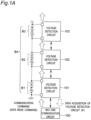
- Fig. 1A is a block diagram of a voltage measurement apparatus showing data acquisition from a voltage detection circuit 101 in a voltage measurement apparatus of a conventional example.
- Fig. 1B is a block diagram of the voltage measurement apparatus showing data acquisition from a voltage detection circuit 103 in the voltage measurement apparatus of the conventional example.
- the voltage measurement apparatus of the conventional example is configured to include a host apparatus 100 made up of a micro control unit (MCU) and a communication circuit, and voltage detection circuits 101, 102 and 103.
- MCU micro control unit
- each of B1, B2 and B3 is a battery cell (hereinafter, referred to as cell).
- BA is an assembled battery configured by connecting the cells B1, B2 and B3 in series.
- the MCU transmits a data readout command to one of the three voltage detection circuits 101, 102 and 103 connected in a daisy chain.
- the command is delivered to all the voltage detection circuits 101, 102 and 103 connected in the daisy chain, and only the voltage detection circuit having become a target transmits reply data.
- the reply data is sequentially delivered through the daisy chain, and the MCU receives the returned data.
- Patent Document 1 Japanese Patent No. JP5503924B2
- the frequency of data transmission in the downstream voltage detection circuit close to the MCU is higher, and the frequency of data transmission in the upstream voltage detection circuit distant from the MCU, is lower.
- a difference generates between the voltage detection circuits, resulting in nonuniformity of the plurality of cell voltages.
- An object of the present invention is to reduce variations in power consumption during communication among a plurality of voltage detection circuits.
- a voltage detection circuit for measuring each cell voltage of an assembled battery configured by connecting a plurality of cells in series.
- the voltage detection circuit is defined as a first voltage detection circuit.
- the voltage detection circuit includes:
- the control circuit controls the reply signal generation circuit, the upstream transfer circuit, and the dummy current consumption circuit to selectively operate one of them. As a result, it is possible to reduce variations in power consumption during communication among the plurality of voltage detection circuits and make the power consumption uniform.
- Fig. 2 is a block diagram showing a configuration example of voltage detection circuits 1, 2 and 3, a voltage measurement apparatus 210, and an assembled battery system 200 according to a first embodiment.
- the assembled battery system 200 is configured to include an assembled battery BA configured by connecting a plurality of cells B1, B2 and B3 in series and a voltage measurement apparatus 210.
- the voltage measurement apparatus 210 includes a host apparatus 50 made up of a micro control unit (MCU) and a communication circuit, and three voltage detection circuits 1, 2 and 3.
- the respective voltage detection circuits 1, 2 and 3 are provided for measuring the cell voltages of the respective cells B1, B2 and B3 of the assembled battery BA. It is noted that the cell voltages of the respective cells B1, B2 and B3 of the assembled battery BA are set to be the same, for example, when the voltage detection circuits 1, 2 and 3 are not connected.
- the host apparatus 50 and the voltage detection circuits 1, 2 and 3 are connected in series in a daisy chain via, for example, a wired line.
- a circuit close to the host apparatus 50 is referred to as a "downstream circuit”
- a circuit distant from the host apparatus 50 is referred to as an "upstream circuit” and the same applies to the other embodiments.
- the voltage detection circuit 1 includes a control circuit 10, a downstream communication circuit 11, an upstream communication circuit 12, a data transmission circuit 13, a data transfer circuit 14, and a dummy data transmission circuit 15.
- the downstream communication circuit 11 has a function of receiving data from the host apparatus 50 and a function of transmitting data to the host apparatus 50.
- the upstream communication circuit 12 has a function of transferring data from the host apparatus 50 to the other voltage detection circuits 2, 3 and a function of receiving data from the other voltage detection circuits 2, 3. Based on the data including a data readout command received by the downstream communication circuit 11 from the host apparatus 50, the control circuit 10 selects any one of the following circuits:
- control circuit 10 controls the downstream communication circuit 11 to transmit data from the selected circuit to the host apparatus 50.
- the control circuit 10 also controls communication operations of the downstream communication circuit 11 and the upstream communication circuit 12.
- the data including the data readout command from the host apparatus 50 includes cell addressing data indicating battery data of which of the cells B1, B2 and B3 is to be read out, and the data is transmitted from the downstream communication circuit 11 to the voltage detection circuit 2 via the upstream communication circuit 12.
- the voltage detection circuit 2 includes a control circuit 20, a downstream communication circuit 21, an upstream communication circuit 22, a data transmission circuit 23, a data transfer circuit 24, and a dummy data transmission circuit 25.
- the downstream communication circuit 21 has a function of receiving data from the host apparatus 50 via the voltage detection circuit 1 and a function of transmitting data to the host apparatus 50 via the voltage detection circuit 1.
- the upstream communication circuit 22 has a function of transferring data received from the host apparatus 50 via the voltage detection circuit 1 to the other voltage detection circuit 3 and a function of receiving data from the other voltage detection circuit 3. Based on the data including the data readout command received by the downstream communication circuit 21 from the host apparatus 50 via the voltage detection circuit 1, the control circuit 20 selects any one of the following circuits:
- control circuit 20 controls the downstream communication circuit 21 to transmit data from the selected circuit to the host apparatus 50 via the voltage detection circuit 1.
- the control circuit 20 also controls communication operations of the downstream communication circuit 21 and the upstream communication circuit 22.
- the data including the data readout command received from the host apparatus 50 via the voltage detection circuit 1 includes cell addressing data indicating battery data of which of the cells B1, B2 and B3 is to be read out.
- the data is transmitted from the downstream communication circuit 21 to the voltage detection circuit 3 via the upstream communication circuit 22.
- the voltage detection circuit 3 includes a control circuit 30, a downstream communication circuit 31, an upstream communication circuit 32, a data transmission circuit 33, a data transfer circuit 34, and a dummy data transmission circuit 35.
- the downstream communication circuit 31 has a function of receiving data from the host apparatus 50 via the voltage detection circuits 1 and 2, and a function of transmitting data to the host apparatus 50 via the voltage detection circuits 2 and 1.
- the upstream communication circuit 32 has a function of transferring data received from the host apparatus 50 via the voltage detection circuits 1 and 2 to the other voltage detection circuit located at the side of upstream (there is no such circuit in the configuration example of Fig. 2 ) and a function of receiving data from the other voltage detection circuit. Based on the data including the data readout command received by the downstream communication circuit 31 from the host apparatus 50 via the voltage detection circuits 1 and 2, the control circuit 30 selects any one of the following circuits:
- control circuit 30 controls the downstream communication circuit 31 such that the downstream communication circuit 31 transmits data from the selected circuit to the host apparatus 50 via the voltage detection circuits 2, 1.
- the control circuit 30 also controls communication operations of the downstream communication circuit 31 and the upstream communication circuit 32.
- the voltage detection circuit 3 is a voltage detection circuit located most upstream, the upstream communication circuit 32 does not receive data from the upstream voltage detection circuit.
- the data including the data readout command received from the host apparatus 50 via the voltage detection circuits 1 and 2 includes cell addressing data indicating battery data of which of the cells B1, B2 and B3 is to be read out.
- the data is transmitted from the downstream communication circuit 31 to the other voltage detection circuit via the upstream communication circuit 32.
- the voltage detection circuit 1, 2, or 3 selectively operates any one of the data transmission circuit 13, 23, or 33, the data transfer circuit 14, 24, or 34, and the dummy data transmission circuit 15, 25, or 35.
- the difference in current consumption related to data communication among the voltage detection circuits 1, 2 and 3 equalize the current consumption or the power consumption of each of the voltage detection circuits 1, 2 and 3 that operates with each of the cell voltages of the cells B1, B2 and B3, and make each of the cell voltages uniform.
- the upstream communication circuit 12, 22, or 32 does not receive data. Hence it is possible to prevent transmission of the dummy data from affecting communication of the downstream voltage detection circuit.
- Fig. 3 is a timing chart showing an operation example of the assembled battery system 200 of Fig. 2 .
- the time for transferring the data may vary among the voltage detection circuits 1, 2 and 3 due to an influence such as variations in reference clock frequency among the voltage detection circuits 1, 2 and 3. If the transmission of the dummy data delays behind the transmission of the data, the transmission of the dummy data may not be in time for the next communication and interferes with the next communication, thus causing a communication error.
- the transmission of the dummy data by performing the transmission of the dummy data at a high communication speed as compared to transmission of ordinary data, it is possible to prevent the above interference and avoid the communication error.
- Fig. 4 is a block diagram showing a configuration example of voltage detection circuits 1A, 2A and 3A, a voltage measurement apparatus 210A, and an assembled battery system 200A according to a second embodiment.
- the assembled battery system 200A is configured to include an assembled battery BA and the voltage measurement apparatus 210A.
- the voltage measurement apparatus 210A includes a host apparatus 50 and three voltage detection circuits 1A, 2A and 3A. Therefore, as compared to the voltage measurement apparatus 210 of Fig. 2 , the voltage measurement apparatus 210A is characterized by including three voltage detection circuits 1A, 2A and 3A in place of three voltage detection circuits 1, 2 and 3.
- the voltage detection circuit 1A is characterized by:
- the voltage detection circuit 2A is characterized by:
- the voltage detection circuit 3A is characterized by:
- control circuits 10A, 20A, 30A control the current value and the on-time of the dummy current circuits 16, 26, 36 such that the power consumption is equal to that upon the data transmission.
- the voltage detection circuit 1A, 2A, or 3A that transmits no data consumes equivalent current by the dummy current circuit 16, 26, or 36, so that it is possible to reduce the difference in current consumption or power consumption in the data transmission among the circuits and make each of the cell voltages uniform.
- Fig. 5 is a block diagram showing a configuration example of voltage detection circuits 1B, 2B and 3B, a voltage measurement apparatus 210B, and an assembled battery system 200B according to a third embodiment of the present invention.
- the assembled battery system 200B is a detailed embodiment, which is made by concretely describing the assembled battery system 200 of Fig. 2 .
- the voltage detection circuits 1B, 2B and 3B are provided in place of the voltage detection circuits 1, 2 and 3, respectively.
- the assembled battery system 200B includes an assembled battery BA configured by connecting cells B1, B2 and B3 in series and the voltage measurement apparatus 210B.
- a host apparatus 50 and three voltage detection circuits 1B, 2B and 3B are connected in series in a daisy chain via, for example, a wired line.
- the voltage detection circuit 1B differs from the voltage detection circuit 1 of Fig. 2 in the following points:
- the voltage detection circuit 2B differs from the voltage detection circuit 2 of Fig. 2 in the following points:
- the voltage detection circuit 3B differs from the voltage detection circuit 3 of Fig. 2 in the following points:
- the host apparatus 50 transmits a communication command having a data readout command that includes cell addressing data to the voltage detection circuits 1B, 2B and 3B.
- the voltage detection circuit 1B transmits a reply signal containing the battery data acquired by the voltage detection circuit 1B to the host apparatus 50.
- the voltage detection circuit 2B transmits a reply signal containing the battery data acquired by the voltage detection circuit 2B to the host apparatus 50 via the voltage detection circuit 1B.
- the voltage detection circuit 3B transmits a reply signal containing the battery data acquired by the voltage detection circuit 3B to the host apparatus 50 via the voltage detection circuits 2B, 1B.
- each of the voltage detection circuits 1B, 2B and 3B is not transmitting the reply signal containing the self-battery data or not transferring the reply signal from the other voltage detection circuit (by each of the upstream transfer circuits 14P, 24P and 34P), each of the dummy reply signal generation circuits 15P, 25P and 35P generates a dummy reply signal and transmits the generated signal to the host apparatus 50 in order to make the cell voltages uniform, in a manner similar to that of the first embodiment.
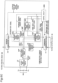
- Fig. 6A is a block diagram showing a detailed configuration example of the voltage detection circuit 1B of Fig. 5 .
- the upstream transfer circuit 14P is configured to include an upstream signal transfer circuit 14A and a downstream signal selection circuit 14B.
- the downstream signal selection circuit 14B performs as follows:
- the battery data acquisition circuit 17 measures the cell voltage of the cell B1, generates battery data including data of the cell voltage, and outputs the generated battery data to the reply signal generation circuit 13P.
- the downstream communication circuit 11 Based on a downstream input and output switching signal (input instruction) from the control circuit 10B, the downstream communication circuit 11 receives the communication command from the host apparatus 50 to output the received command to the control circuit 10B, and transmits the received command to the voltage detection circuit 2B via the downstream transfer circuit 18 and the upstream communication circuit 12.
- the downstream communication circuit 11 transmits a signal from the downstream signal selection circuit 14B to the host apparatus 50.
- the upstream communication circuit 12 Based on an upstream input and output switching signal (output instruction) from the control circuit 10B, the upstream communication circuit 12 transmits to the voltage detection circuit 2B the communication command inputted from the host apparatus 50 via the downstream communication circuit 11 and the downstream transfer circuit 18. In addition, based on the upstream input and output switching signal (input instruction) from the control circuit 10B, the upstream communication circuit 12 receives an upstream reply signal from the voltage detection circuit 2B, and transmits the upstream reply signal to the host apparatus 50 via the following:
- Fig. 6B is a block diagram showing a detailed configuration example of the voltage detection circuit 2B of Fig. 5 .
- the upstream transfer circuit 24P is configured to include an upstream signal transfer circuit 24A and a downstream signal selection circuit 24B.
- the downstream signal selection circuit 34B performs as follows:
- the battery data acquisition circuit 27 measures the cell voltage of the cell B2, generates battery data including data of the cell voltage, and outputs the generated battery data to the reply signal generation circuit 23P.
- Each of the circuits 21 to 25P of the voltage detection circuit 2B operates in a manner similar to each of the circuits 11 to 15P of Fig. 6A .
- Fig. 6C is a block diagram showing a detailed configuration example of the voltage detection circuit 3B of Fig. 5 .
- the upstream transfer circuit 34P is configured to include an upstream signal transfer circuit 34A and a downstream signal selection circuit 34B.
- the downstream signal selection circuit 34B performs as follows:
- the battery data acquisition circuit 37 measures the cell voltage of the cell B3, generates battery data including data of the cell voltage, and outputs the generated battery data to the reply signal generation circuit 33P.
- Each of the circuits 31 to 35P of the voltage detection circuit 3B operates in a manner similar to each of the circuits 11 to 15P of Fig. 6A .
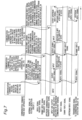
- Fig. 7 is a timing chart showing an operation example of the assembled battery system 200B of Fig. 5 .
- the operation of the voltage detection circuit 2B provided between the voltage detection circuit 1B and the voltage detection circuit 3B will be described below.
- the control circuit 20B of the voltage detection circuit 2B upon receiving the communication command (addressed to the cell B2) from the host apparatus 50 to the voltage detection circuit 2B, the control circuit 20B of the voltage detection circuit 2B outputs the downstream input and output switching signal (output instruction) to the downstream communication circuit 21, and the downstream communication circuit 21 is switched over from an input mode to an output mode.
- the control circuit 20B outputs a reply signal containing the battery data on the cell B2, following an ACK (Acknowledgement) signal, from the reply signal generation circuit 23P to the host apparatus 50 via the downstream signal selection circuit 24B, the downstream communication circuit 21, and the voltage detection circuit 1B.
- the downstream communication circuit 21 is switched over from the output mode to the input mode based on the downstream input and output switching signal (input instruction) from the control circuit 20B.
- the control circuit 20B of the voltage detection circuit 2B outputs the downstream input and output switching signal (output instruction) to the downstream communication circuit 21, and the downstream communication circuit 21 is switched over from the input mode to the output mode.
- the control circuit 20B transmits a dummy reply signal from the dummy reply signal generation circuit 25P to the host apparatus 50 via the downstream signal selection circuit 24B, the downstream communication circuit 21, and the voltage detection circuit 1B.
- the downstream communication circuit 21 is switched over from the output mode to the input mode based on the downstream input and output switching signal (input instruction) from the control circuit 20B.
- the control circuit 20B of the voltage detection circuit 2B outputs the downstream input and output switching signal (output instruction) to the downstream communication circuit 21, and the downstream communication circuit 21 is switched over from the input mode to the output mode.
- the control circuit 20B transmits an upstream reply signal, which is received by the upstream communication circuit 22, from the upstream signal transfer circuit 24A to the host apparatus 50 via the downstream signal selection circuit 24B, the downstream communication circuit 21, and the voltage detection circuit 1B.
- the downstream communication circuit 21 is switched over from the output mode to the input mode based on the downstream input and output switching signal (input instruction) from the control circuit 20B.
- the voltage detection circuit 1B, 2B, or 3B selectively operates any one of the reply signal generation circuit 13P, 23P, or 33P, the upstream transfer circuit 14P, 24P, or 34P, and the dummy reply signal generation circuit 15P, 25P, or 35P.
- the difference in current consumption related to data communication among the voltage detection circuits 1B, 2B and 3B equalize the current consumption or the power consumption of each of the voltage detection circuits 1B, 2B and 3B that operates with each of the cell voltages of the cells B1, B2 and B3, and make each of the cell voltages uniform.
- the communication speed of the dummy reply signal generated by the dummy reply signal generation circuit 15P is set to be higher than the communication speed of the reply signal generated by the reply signal generation circuit 13P, for example.
- the upstream communication circuit 32 of the voltage detection circuit 3B that detects the cell voltage of the most upstream cell selected from the plurality of cells does not receive the dummy reply signal from the voltage detection circuit located at the side of upstream, since there is no voltage detection circuit located at the side of upstream.
- the battery data acquisition circuit 17, 27 and 37 measure the cell voltages of the cells B1, B2 and B3, respectively, and generate battery data including data of cell voltages to the reply signal generation circuit 13P, 23P and 33P.
- the reply signal generation circuit 13P, 23P and 33P generate and transmits a reply signal containing battery data on the cells B1, B2 and B3, respectively.
- the battery data includes the following data instead of the battery data containing data of the cell voltages, or includes the following data in addition to the battery data containing data of the cell voltages.
- the battery data may include detection data or data stored in a register such as an abnormality detection, an abnormality detection voltage, and an operation control set value at the inside of the voltage detection circuits 1B, 2B and 3B, each of which is configured by an Integrated Circuit (IC) etc. This is the same in the following embodiments.
- IC Integrated Circuit
- Fig. 8 is a block diagram showing a configuration example of voltage detection circuits 1C, 2C and 3C, a voltage measurement apparatus 210C, and an assembled battery system 200C according to a fourth embodiment.
- the assembled battery system 200C is a detailed embodiment making the assembled battery system 200A of Fig. 4 more specific, and as compared to the assembled battery system 200A of Fig. 4 , the voltage detection circuits 1C, 2C and 3C are provided in place of the voltage detection circuits 1A, 2A and 3A, respectively.
- the assembled battery system 200C includes an assembled battery BA configured by connecting cells B1, B2 and B3 in series and the voltage measurement apparatus 210C.
- a host apparatus 50 and three voltage detection circuits 1C, 2C and 3C are connected in series in a daisy chain via, for example, a wired line.
- Fig. 9A is a block diagram showing a detailed configuration example of the voltage detection circuit 1C of Fig. 8 .
- Fig. 9B is a block diagram showing a detailed configuration example of the voltage detection circuit 2C of Fig. 8 .
- Fig. 9C is a block diagram showing a detailed configuration example of the voltage detection circuit 3C of Fig. 8 .
- the voltage detection circuit 1C of Fig. 9A is characterized by the following steps:
- the dummy current generation circuit 16P generates a predetermined dummy current based on a dummy current generation request signal from the control circuit 10B. It is noted that the dummy current generation request signal is output only from the control circuit 10B to the dummy current generation circuit 16P.
- the voltage detection circuit 2C of Fig. 9B is characterized by the following steps:
- the dummy current generation circuit 26P generates a predetermined dummy current based on a dummy current generation request signal from the control circuit 20B. It is noted that the dummy current generation request signal is output only from the control circuit 20B to the dummy current generation circuit 26P.
- the voltage detection circuit 3C of Fig. 9C is characterized by the following steps:
- the dummy current generation circuit 36P generates a predetermined dummy current based on a dummy current generation request signal from the control circuit 30B. It is noted that the dummy current generation request signal is output only from the control circuit 30B to the dummy current generation circuit 36P.
- Fig. 10 is a timing chart showing an operation example of the assembled battery system 200C of Fig. 8 .
- the operation of the voltage detection circuit 2C provided between the voltage detection circuit 1C and the voltage detection circuit 3C will be described below.
- the control circuit 20C of the voltage detection circuit 2C upon receiving the communication command (addressed to the cell B2) from the host apparatus 50 to the voltage detection circuit 2C, the control circuit 20C of the voltage detection circuit 2C outputs the downstream input and output switching signal (output instruction) to the downstream communication circuit 21, and the downstream communication circuit 21 is switched over from an input mode to an output mode.
- the control circuit 20C outputs a reply signal containing the battery data on the cell B2, following an ACK signal, from the reply signal generation circuit 23P to the host apparatus 50 via the downstream signal selection circuit 24B, the downstream communication circuit 21, and the voltage detection circuit 1C.
- the downstream communication circuit 21 is switched over from the output mode to the input mode based on the downstream input and output switching signal (input instruction) from the control circuit 20C.
- the control circuit 20C of the voltage detection circuit 2C outputs the dummy current generation request signal to the dummy current generation circuit 26P so that the dummy current generation circuit 26P generates a predetermined dummy current.
- the control circuit 20C of the voltage detection circuit 2C outputs the downstream input and output switching signal (output instruction) to the downstream communication circuit 21, and the downstream communication circuit 21 is switched over from the input mode to the output mode.
- the control circuit 20C transmits an upstream reply signal, which is received by the upstream communication circuit 22, from the upstream signal transfer circuit 24A to the host apparatus 50 via the downstream signal selection circuit 24B, the downstream communication circuit 21, and the voltage detection circuit 1C.
- the downstream communication circuit 21 is switched from the output mode to the input mode based on the downstream input and output switching signal (input instruction) from the control circuit 20C.
- the voltage detection circuit 1C, 2C, or 3C selectively operates any one of the reply signal generation circuit 13P, 23P, or 33P, the upstream transfer circuit 14P, 24P, or 34P, and the dummy current generation circuit 16P, 26P, or 36P.
- the difference in current consumption related to data communication among the voltage detection circuits 1C, 2C and 3C equalize the current consumption or the power consumption of each of the voltage detection circuits 1C, 2C and 3C that operates with each of the cell voltages of the cells B1, B2 and B3, and make each of the cell voltages uniform.
- the dummy reply signal generation circuits 15P, 25P and 35P according to the third embodiment consume a predetermined dummy current by generating the dummy reply signal.
- the dummy current generation circuits 16P, 26P and 36P according to the fourth embodiment consume a predetermined dummy current by generating the dummy current. Therefore, both the dummy reply signal generation circuits 15P, 25P and 35P and the dummy current generation circuits 16P, 26P and 36P can be regarded as the dummy current consumption circuit.
- the power consumption of the upstream transfer circuits 14P, 24P and 34P, the power consumption of the reply signal generation circuits 13P, 23P and 33P, the power consumption of the dummy reply signal generation circuits 15P, 25P and 35P, and the power consumption of the dummy current generation circuits 16P, 26P and 36P are the same as each other.
- Figs. 11A to 11C are block diagrams showing scheme examples of a communication line between an upstream voltage detection circuit 4A and a downstream voltage detection circuit 4B (corresponding to two adjacent voltage detection circuits selected from the voltage detection circuits (1, 2 and 3), (1A, 2A and 3A), (1B, 2B and 3B), (1C, 2C and 3C) of the first to fourth embodiments).
- Figs. 11A to 11C show configuration examples of a daisy-chain connection communication scheme between the voltage detection circuits.
Landscapes
- Chemical & Material Sciences (AREA)
- Chemical Kinetics & Catalysis (AREA)
- Electrochemistry (AREA)
- General Chemical & Material Sciences (AREA)
- Engineering & Computer Science (AREA)
- Physics & Mathematics (AREA)
- General Physics & Mathematics (AREA)
- Manufacturing & Machinery (AREA)
- Power Engineering (AREA)
- Secondary Cells (AREA)
- Charge And Discharge Circuits For Batteries Or The Like (AREA)
- Measurement Of Current Or Voltage (AREA)
Description
- The present invention relates to a voltage detection circuit, a voltage measurement apparatus, and an assembled battery system. A voltage detection circuit reflecting the preamble of
present claim 1 is disclosed by the documentWO 2009/106952 . -
Fig. 1A is a block diagram of a voltage measurement apparatus showing data acquisition from avoltage detection circuit 101 in a voltage measurement apparatus of a conventional example.Fig. 1B is a block diagram of the voltage measurement apparatus showing data acquisition from avoltage detection circuit 103 in the voltage measurement apparatus of the conventional example. Referring toFigs. 1A and1B , the voltage measurement apparatus of the conventional example is configured to include ahost apparatus 100 made up of a micro control unit (MCU) and a communication circuit, andvoltage detection circuits - In the conventional example, as shown in
Fig. 1A , the MCU transmits a data readout command to one of the threevoltage detection circuits voltage detection circuits - [Patent Document 1] Japanese Patent No.
JP5503924B2 -
- In the conventional example, the frequency of data transmission in the downstream voltage detection circuit close to the MCU is higher, and the frequency of data transmission in the upstream voltage detection circuit distant from the MCU, is lower. As a result, in current consumption or power consumption during data communication, a difference generates between the voltage detection circuits, resulting in nonuniformity of the plurality of cell voltages.
- An object of the present invention is to reduce variations in power consumption during communication among a plurality of voltage detection circuits.
- According to one aspect of the present invention, there is provided a voltage detection circuit, as defined in
present claim 1, for measuring each cell voltage of an assembled battery configured by connecting a plurality of cells in series. The voltage detection circuit is defined as a first voltage detection circuit. The voltage detection circuit includes: - a reply signal generation circuit that generates a reply signal containing data detected by the first voltage detection circuit;
- an upstream transfer circuit that transfers a signal received by an upstream communication circuit to downstream;
- a dummy current consumption circuit that consumes a predetermined dummy current; and
- a control circuit that controls the reply signal generation circuit, the upstream transfer circuit, and the dummy current consumption circuit to selectively operate any one of the reply signal generation circuit, the upstream transfer circuit, and the dummy current consumption circuit, based on a communication command signal.
- Therefore, according to the present invention, based on a communication command signal received from the host apparatus, the control circuit controls the reply signal generation circuit, the upstream transfer circuit, and the dummy current consumption circuit to selectively operate one of them. As a result, it is possible to reduce variations in power consumption during communication among the plurality of voltage detection circuits and make the power consumption uniform.
-
-
Fig. 1A is a block diagram of a voltage measurement apparatus showing data acquisition from avoltage detection circuit 101 in a voltage measurement apparatus of a conventional example. -
Fig. 1B is a block diagram of the voltage measurement apparatus showing data acquisition from avoltage detection circuit 103 in the voltage measurement apparatus of the conventional example. -
Fig. 2 is a block diagram showing a configuration example ofvoltage detection circuits voltage measurement apparatus 210, and an assembledbattery system 200 according to a first embodiment not forming part of the present invention. -
Fig. 3 is a timing chart showing an operation example of the assembledbattery system 200 ofFig. 2 . -
Fig. 4 is a block diagram showing a configuration example ofvoltage detection circuits voltage measurement apparatus 210A, and an assembledbattery system 200A according to a second embodiment not forming part of the present invention. -
Fig. 5 is a block diagram showing a configuration example ofvoltage detection circuits voltage measurement apparatus 210B, and an assembledbattery system 200B according to a third embodiment of the present invention. -
Fig. 6A is a block diagram showing a detailed configuration example of thevoltage detection circuit 1B ofFig. 5 . -
Fig. 6B is a block diagram showing a detailed configuration example of thevoltage detection circuit 2B ofFig. 5 . -
Fig. 6C is a block diagram showing a detailed configuration example of thevoltage detection circuit 3B ofFig. 5 . -
Fig. 7 is a timing chart showing an operation example of the assembledbattery system 200B ofFig. 5 . -
Fig. 8 is a block diagram showing a configuration example ofvoltage detection circuits voltage measurement apparatus 210C, and an assembledbattery system 200C according to a fourth embodiment not forming part of the present invention. -
Fig. 9A is a block diagram showing a detailed configuration example of thevoltage detection circuit 1C ofFig. 8 . -
Fig. 9B is a block diagram showing a detailed configuration example of thevoltage detection circuit 2C ofFig. 8 . -
Fig. 9C is a block diagram showing a detailed configuration example of thevoltage detection circuit 3C ofFig. 8 . -
Fig. 10 is a timing chart showing an operation example of the assembledbattery system 200C ofFig. 8 . -
Fig. 11A is a block diagram showing a scheme example 1 of a communication line between an upstreamvoltage detection circuit 4A and a downstreamvoltage detection circuit 4B according to a first modified embodiment. -
Fig. 11B is a block diagram showing a scheme example 2 of the communication line between the upstreamvoltage detection circuit 4A and the downstreamvoltage detection circuit 4B according to the first modified embodiment. -
Fig. 11C is a block diagram showing a scheme example 3 of the communication line between the upstreamvoltage detection circuit 4A and the downstreamvoltage detection circuit 4B according to the first modified embodiment. - Hereinafter, embodiments of the present invention will be described. In this case, the same or similar constituent elements will be provided with the same reference numerals, and the detailed description thereof will be omitted.
-
Fig. 2 is a block diagram showing a configuration example ofvoltage detection circuits voltage measurement apparatus 210, and an assembledbattery system 200 according to a first embodiment. - Referring to
Fig. 2 , the assembledbattery system 200 is configured to include an assembled battery BA configured by connecting a plurality of cells B1, B2 and B3 in series and avoltage measurement apparatus 210. In this case, thevoltage measurement apparatus 210 includes ahost apparatus 50 made up of a micro control unit (MCU) and a communication circuit, and threevoltage detection circuits voltage detection circuits voltage detection circuits host apparatus 50 and thevoltage detection circuits host apparatus 50 is referred to as a "downstream circuit", and a circuit distant from thehost apparatus 50 is referred to as an "upstream circuit", and the same applies to the other embodiments. - The
voltage detection circuit 1 includes acontrol circuit 10, adownstream communication circuit 11, anupstream communication circuit 12, adata transmission circuit 13, adata transfer circuit 14, and a dummydata transmission circuit 15. Thedownstream communication circuit 11 has a function of receiving data from thehost apparatus 50 and a function of transmitting data to thehost apparatus 50. Theupstream communication circuit 12 has a function of transferring data from thehost apparatus 50 to the othervoltage detection circuits voltage detection circuits downstream communication circuit 11 from thehost apparatus 50, thecontrol circuit 10 selects any one of the following circuits: - (1) the
data transmission circuit 13 that transmits battery data (including information such as a cell voltage, the same applies hereinafter) of the cell B1; - (2) the dummy
data transmission circuit 15 that transmits predetermined dummy data; and - (3) the
data transfer circuit 14 that transfers data received by theupstream communication circuit 12. - Then the
control circuit 10 controls thedownstream communication circuit 11 to transmit data from the selected circuit to thehost apparatus 50. Thecontrol circuit 10 also controls communication operations of thedownstream communication circuit 11 and theupstream communication circuit 12. - The data including the data readout command from the
host apparatus 50 includes cell addressing data indicating battery data of which of the cells B1, B2 and B3 is to be read out, and the data is transmitted from thedownstream communication circuit 11 to thevoltage detection circuit 2 via theupstream communication circuit 12. - (A) When the cell addressing data is addressed to the cell B1, the
control circuit 10 controls thedata transmission circuit 13 and thedownstream communication circuit 11 such that the battery data of thecell B 1 is transmitted from thedata transmission circuit 13 to thehost apparatus 50 via thedownstream communication circuit 11. - (B) When the cell addressing data is addressed to the cell B2 or B3 located at the side of upstream which is more distant than the
voltage detection circuit 1 as seen from thehost apparatus 50, thecontrol circuit 10 controls thedata transfer circuit 14 to transmit the data received by theupstream communication circuit 12 to thehost apparatus 50 via thedownstream communication circuit 11. - (C) When the cell addressing data is addressed to a cell located at the side of downstream which is closer than the
voltage detection circuit 1 as seen from thehost apparatus 50, there is no cell located at the side of downstream of the cell B1. Therefore, thecontrol circuit 10 does not control the dummydata transmission circuit 15 to generate dummy data and transmit the generated data to thehost apparatus 50. - The
voltage detection circuit 2 includes acontrol circuit 20, adownstream communication circuit 21, anupstream communication circuit 22, adata transmission circuit 23, adata transfer circuit 24, and a dummydata transmission circuit 25. Thedownstream communication circuit 21 has a function of receiving data from thehost apparatus 50 via thevoltage detection circuit 1 and a function of transmitting data to thehost apparatus 50 via thevoltage detection circuit 1. Theupstream communication circuit 22 has a function of transferring data received from thehost apparatus 50 via thevoltage detection circuit 1 to the othervoltage detection circuit 3 and a function of receiving data from the othervoltage detection circuit 3. Based on the data including the data readout command received by thedownstream communication circuit 21 from thehost apparatus 50 via thevoltage detection circuit 1, thecontrol circuit 20 selects any one of the following circuits: - (1) the
data transmission circuit 23 that transmits battery data of the cell B2; - (2) the dummy
data transmission circuit 25 that transmits predetermined dummy data; and - (3) the
data transfer circuit 24 that transfers data received by theupstream communication circuit 22. - Then, the
control circuit 20 controls thedownstream communication circuit 21 to transmit data from the selected circuit to thehost apparatus 50 via thevoltage detection circuit 1. Thecontrol circuit 20 also controls communication operations of thedownstream communication circuit 21 and theupstream communication circuit 22. - The data including the data readout command received from the
host apparatus 50 via thevoltage detection circuit 1 includes cell addressing data indicating battery data of which of the cells B1, B2 and B3 is to be read out. The data is transmitted from thedownstream communication circuit 21 to thevoltage detection circuit 3 via theupstream communication circuit 22. - (A) When the cell addressing data is addressed to the cell B2, the
control circuit 20 controls thedata transmission circuit 23 and thedownstream communication circuit 21 such that the battery data of the cell B2 is transmitted from thedata transmission circuit 23 to thehost apparatus 50 via thedownstream communication circuit 21 and thevoltage detection circuit 1. - (B) When the cell addressing data is addressed to the cell B3 located at the side of upstream which is more distant than the
voltage detection circuit 1 as seen from thehost apparatus 50, thecontrol circuit 20 controls thedata transfer circuit 24 to transmit the data received by theupstream communication circuit 22 to thehost apparatus 50 via thedownstream communication circuit 21 and thevoltage detection circuit 1. - (C) When the cell addressing data is addressed to the cell B1 located at the side of downstream which is closer than the
voltage detection circuit 1 as seen from thehost apparatus 50, thecontrol circuit 20 controls the dummydata transmission circuit 25 to generate dummy data and transmit the generated data to thehost apparatus 50. - The
voltage detection circuit 3 includes acontrol circuit 30, adownstream communication circuit 31, anupstream communication circuit 32, adata transmission circuit 33, adata transfer circuit 34, and a dummydata transmission circuit 35. Thedownstream communication circuit 31 has a function of receiving data from thehost apparatus 50 via thevoltage detection circuits host apparatus 50 via thevoltage detection circuits upstream communication circuit 32 has a function of transferring data received from thehost apparatus 50 via thevoltage detection circuits Fig. 2 ) and a function of receiving data from the other voltage detection circuit. Based on the data including the data readout command received by thedownstream communication circuit 31 from thehost apparatus 50 via thevoltage detection circuits control circuit 30 selects any one of the following circuits: - (1) the
data transmission circuit 33 that transmits battery data of the cell B3; - (2) the dummy
data transmission circuit 35 that transmits predetermined dummy data; and - (3) the
data transfer circuit 34 that transfers data received by theupstream communication circuit 32. - Then the
control circuit 30 controls thedownstream communication circuit 31 such that thedownstream communication circuit 31 transmits data from the selected circuit to thehost apparatus 50 via thevoltage detection circuits control circuit 30 also controls communication operations of thedownstream communication circuit 31 and theupstream communication circuit 32. When thevoltage detection circuit 3 is a voltage detection circuit located most upstream, theupstream communication circuit 32 does not receive data from the upstream voltage detection circuit. - The data including the data readout command received from the
host apparatus 50 via thevoltage detection circuits downstream communication circuit 31 to the other voltage detection circuit via theupstream communication circuit 32. - (A) When the cell addressing data is addressed to the cell B3, the
control circuit 30 controls thedata transmission circuit 33 and thedownstream communication circuit 31 such that the battery data of the cell B3 is transmitted from thedata transmission circuit 33 to thehost apparatus 50 via thedownstream communication circuit 31 and thevoltage detection circuits - (B) When the cell addressing data is addressed to the cell located at the side of upstream which is more distant than the
voltage detection circuit 1 as seen from thehost apparatus 50, there is no cell located at the side of downstream of the cell B1. Therefore, thecontrol circuit 30 does not control thedata transfer circuit 34 to transmit the data received by theupstream communication circuit 32 to thehost apparatus 50 via thedownstream communication circuit 31 and thevoltage detection circuits - (C) When the cell addressing data is addressed to the cell B1 or B2 located at the side of downstream which is closer than the
voltage detection circuit 1 as seen from thehost apparatus 50, thecontrol circuit 30 controls the dummydata transmission circuit 35 to generate dummy data and transmit the generated data to thehost apparatus 50. - As described above, according to the present embodiment,
- (A) When the data including the data readout command received from the
host apparatus 50 is directed to the self-voltage detection circuit control circuit data transmission circuit host apparatus 50. - (B) When the data including the data readout command received from the
host apparatus 50 is an upstream voltage detection circuit more distant from thehost apparatus 50 side than the self-voltage detection circuit control circuit data transfer circuits upstream communication circuit host apparatus 50 via thedownstream communication circuit - (C) When the data including the data readout command received from the
host apparatus 50 is a downstream voltage detection circuit closer to thehost apparatus 50 side than the self-voltage detection circuit control circuit data transmission circuit host apparatus 50 via thedownstream communication circuit - According to the present embodiment, at the time of data readout from any of the
voltage detection circuits voltage detection circuit data transmission circuit data transfer circuit data transmission circuit voltage detection circuits voltage detection circuits - In the embodiment described above, when the data received from the
host apparatus 50 side is directed to the self-voltage detection circuit voltage detection circuit host apparatus 50 side than the self-voltage detection circuit upstream communication circuit -
Fig. 3 is a timing chart showing an operation example of the assembledbattery system 200 ofFig. 2 . - As shown in
Fig. 3 , by performing transmission of the dummy data at a high communication speed as compared to transmission of data related to ordinary battery data, it is possible to prevent the transmission of the dummy data from interfering with transmission of next data. In addition, when increasing of the communication speed affects the power consumption, by setting the current consumption during communication upon transmitting the dummy data to a predetermined value so that the power consumption is the same as that upon transmitting the data, it is possible to equalize the current consumption or the power consumption among thevoltage detection circuits - For example, even when the data is transmitted at the same communication speed, the time for transferring the data may vary among the
voltage detection circuits voltage detection circuits - In the case of a scheme in which the communication speed affects the current consumption, by compensating the current consumption during communication to obtain the same power consumption as that upon the data transmission, it is possible to compensate the power consumption for the speed change and reduce variations in power consumption among the
voltage detection circuits -
Fig. 4 is a block diagram showing a configuration example ofvoltage detection circuits voltage measurement apparatus 210A, and an assembledbattery system 200A according to a second embodiment. - Referring to
Fig. 4 , the assembledbattery system 200A is configured to include an assembled battery BA and thevoltage measurement apparatus 210A. Thevoltage measurement apparatus 210A includes ahost apparatus 50 and threevoltage detection circuits voltage measurement apparatus 210 ofFig. 2 , thevoltage measurement apparatus 210A is characterized by including threevoltage detection circuits voltage detection circuits - As compared to the
voltage detection circuit 1 ofFig. 2 , thevoltage detection circuit 1A is characterized by: - (1) including a
control circuit 10A in place of thecontrol circuit 10; and - (2) including a dummy
current circuit 16 in place of the dummydata transmission circuit 15. That is, thecontrol circuit 10A contributes to the uniformity of current consumption or power consumption by controlling the dummycurrent circuit 16 to operate and generate a dummy current instead of causing the dummydata transmission circuit 15 to perform the transmission operation. - As compared to the
voltage detection circuit 2 ofFig. 2 , thevoltage detection circuit 2A is characterized by: - (1) including a
control circuit 20A in place of thecontrol circuit 20; and - (2) including a dummy
current circuit 26 in place of the dummydata transmission circuit 25. That is, thecontrol circuit 20A contributes to the uniformity of current consumption or power consumption by controlling the dummycurrent circuit 26 to operate and generate a dummy current instead of causing the dummydata transmission circuit 25 to perform the transmission operation. - As compared to the
voltage detection circuit 3 ofFig. 2 , thevoltage detection circuit 3A is characterized by: - (1) including a
control circuit 30A in place of thecontrol circuit 30; and - (2) including a dummy
current circuit 36 in place of the dummydata transmission circuit 35. That is, thecontrol circuit 30A contributes to the uniformity of current consumption or power consumption by controlling the dummycurrent circuit 36 to operate and generate a dummy current instead of causing the dummydata transmission circuit 35 to perform the transmission operation. - That is, the
control circuits current circuits - Therefore, according to the present embodiment, at the time of data readout from any of the
voltage detection circuits voltage detection circuit current circuit -
Fig. 5 is a block diagram showing a configuration example ofvoltage detection circuits voltage measurement apparatus 210B, and an assembledbattery system 200B according to a third embodiment of the present invention. Referring toFig. 5 , the assembledbattery system 200B is a detailed embodiment, which is made by concretely describing the assembledbattery system 200 ofFig. 2 . As compared to the assembledbattery system 200 ofFig. 2 , thevoltage detection circuits voltage detection circuits - Referring to
Fig. 5 , the assembledbattery system 200B includes an assembled battery BA configured by connecting cells B1, B2 and B3 in series and thevoltage measurement apparatus 210B. In thevoltage measurement apparatus 210B, ahost apparatus 50 and threevoltage detection circuits - The
voltage detection circuit 1B differs from thevoltage detection circuit 1 ofFig. 2 in the following points: - (1) In place of the
control circuit 10, acontrol circuit 10B is provided. - (2) A battery
data acquisition circuit 17 and adownstream transfer circuit 18 are explicitly specified. - (3) In place of the
data transmission circuit 13, a replysignal generation circuit 13P corresponding to thedata transmission circuit 13 is provided. - (4) In place of the
data transfer circuit 14, anupstream transfer circuit 14P corresponding to thedata transfer circuit 14 is provided. - (5) In place of the dummy
data transmission circuit 15, a dummy replysignal generation circuit 15P corresponding to the dummydata transmission circuit 15 is provided. - The
voltage detection circuit 2B differs from thevoltage detection circuit 2 ofFig. 2 in the following points: - (1) In place of the
control circuit 20, acontrol circuit 20B is provided. - (2) A battery
data acquisition circuit 27 and adownstream transfer circuit 28 are explicitly specified. - (3) In place of the
data transmission circuit 23, a replysignal generation circuit 23P corresponding to thedata transmission circuit 23 is provided. - (4) In place of the
data transfer circuit 24, anupstream transfer circuit 24P corresponding to thedata transfer circuit 24 is provided. - (5) In place of the dummy
data transmission circuit 25, a dummy replysignal generation circuit 25P corresponding to the dummydata transmission circuit 25 is provided. - The
voltage detection circuit 3B differs from thevoltage detection circuit 3 ofFig. 2 in the following points: - (1) In place of the
control circuit 30, acontrol circuit 30B is provided. - (2) A battery
data acquisition circuit 37 and adownstream transfer circuit 38 are explicitly specified. - (3) In place of the
data transmission circuit 33, a replysignal generation circuit 33P corresponding to thedata transmission circuit 33 is provided. - (4) In place of the
data transfer circuit 34, anupstream transfer circuit 34P corresponding to thedata transfer circuit 34 is provided. - (5) In place of the dummy
data transmission circuit 35, a dummy replysignal generation circuit 35P corresponding to the dummydata transmission circuit 35 is provided. - Referring to
Fig. 5 , thehost apparatus 50 transmits a communication command having a data readout command that includes cell addressing data to thevoltage detection circuits host apparatus 50 is the cell B1, thevoltage detection circuit 1B transmits a reply signal containing the battery data acquired by thevoltage detection circuit 1B to thehost apparatus 50. When the cell addressing data in the communication command from thehost apparatus 50 is the cell B2, thevoltage detection circuit 2B transmits a reply signal containing the battery data acquired by thevoltage detection circuit 2B to thehost apparatus 50 via thevoltage detection circuit 1B. When the cell addressing data in the communication command from thehost apparatus 50 is the cell B3, thevoltage detection circuit 3B transmits a reply signal containing the battery data acquired by thevoltage detection circuit 3B to thehost apparatus 50 via thevoltage detection circuits voltage detection circuits upstream transfer circuits signal generation circuits host apparatus 50 in order to make the cell voltages uniform, in a manner similar to that of the first embodiment. - Hereinafter, configurations of the
voltage detection circuits Figs. 6A to 6C . -
Fig. 6A is a block diagram showing a detailed configuration example of thevoltage detection circuit 1B ofFig. 5 . Referring toFig. 6A , theupstream transfer circuit 14P is configured to include an upstreamsignal transfer circuit 14A and a downstreamsignal selection circuit 14B. In this case, the downstreamsignal selection circuit 14B performs as follows: - (1) When receiving a reply signal request signal from the
control circuit 10B, the downstreamsignal selection circuit 14B selects a reply signal from the replysignal generation circuit 13P, and outputs the selected signal to thedownstream communication circuit 11. - (2) When receiving an upstream transfer request signal from the
control circuit 10B, the downstreamsignal selection circuit 14B selects an upstream reply signal from the upstreamsignal transfer circuit 14A, and outputs the selected signal to thedownstream communication circuit 11. - (3) When receiving a dummy reply signal request signal from the
control circuit 10B, the downstreamsignal selection circuit 14B selects a dummy reply signal from the dummy replysignal generation circuit 15P, and outputs the selected signal to thedownstream communication circuit 11. - Referring to
Fig. 6A , the batterydata acquisition circuit 17 measures the cell voltage of the cell B1, generates battery data including data of the cell voltage, and outputs the generated battery data to the replysignal generation circuit 13P. Based on a downstream input and output switching signal (input instruction) from thecontrol circuit 10B, thedownstream communication circuit 11 receives the communication command from thehost apparatus 50 to output the received command to thecontrol circuit 10B, and transmits the received command to thevoltage detection circuit 2B via thedownstream transfer circuit 18 and theupstream communication circuit 12. In addition, based on the downstream input and output switching signal (output instruction) from thecontrol circuit 10B, thedownstream communication circuit 11 transmits a signal from the downstreamsignal selection circuit 14B to thehost apparatus 50. Based on an upstream input and output switching signal (output instruction) from thecontrol circuit 10B, theupstream communication circuit 12 transmits to thevoltage detection circuit 2B the communication command inputted from thehost apparatus 50 via thedownstream communication circuit 11 and thedownstream transfer circuit 18. In addition, based on the upstream input and output switching signal (input instruction) from thecontrol circuit 10B, theupstream communication circuit 12 receives an upstream reply signal from thevoltage detection circuit 2B, and transmits the upstream reply signal to thehost apparatus 50 via the following: - (1) the upstream
signal transfer circuit 14A that performs a transfer operation based on the upstream transfer request signal from thecontrol circuit 10B; - (2) the downstream
signal selection circuit 14B that performs a selection operation based on the upstream transfer request signal from thecontrol circuit 10B; and - (3) the
downstream communication circuit 11 that performs a transmission operation based on the downstream input and output switching signal (output instruction) from thecontrol circuit 10B. -
- (A) In a wait state of the communication command from the
host apparatus 50, thecontrol circuit 10B outputs the downstream input and output switching signal (input instruction) to thedownstream communication circuit 11, and outputs the upstream input and output switching signal (output instruction) to theupstream communication circuit 12. When receiving the communication command from thehost apparatus 50, thecontrol circuit 10B performs control as follows by outputting the downstream input and output switching signal (output instruction) to thedownstream communication circuit 11, and outputting the upstream input and output switching signal (input instruction) to theupstream communication circuit 12. Thereafter, thecontrol circuit 10B returns to the wait state of the communication command from thehost apparatus 50. - (B) When the self-cell B1 is explicitly specified as the data readout command in the communication command received by the
downstream communication circuit 11, thecontrol circuit 10B outputs the reply signal request signal to the replysignal generation circuit 13P and the downstreamsignal selection circuit 14B. At this time, the replysignal generation circuit 13P generates a reply signal containing battery data on the cell voltage of the cell B1, and transmits the reply signal to thehost apparatus 50 via the downstreamsignal selection circuit 14B and thedownstream communication circuit 11. - (C) When the cells B2 and B3 of the
voltage detection circuits voltage detection circuit 1B are explicitly specified as the data readout command in the communication command received by thedownstream communication circuit 11, thecontrol circuit 10B outputs the upstream transfer request signal to the upstreamsignal transfer circuit 14A and the downstreamsignal selection circuit 14B. At this time, theupstream communication circuit 12 transmits the received upstream reply signal to thehost apparatus 50 via the upstreamsignal transfer circuit 14A, the downstreamsignal selection circuit 14B, and thedownstream communication circuit 11. - (D) When the cell of the voltage detection circuit located at the side of downstream of the
voltage detection circuit 1B is explicitly specified as the data readout command in the communication command received by thedownstream communication circuit 11, thecontrol circuit 10B transmits the dummy reply signal request signal to the dummy replysignal generation circuit 15P and the downstreamsignal selection circuit 14B. At this time, the dummy replysignal generation circuit 15P generates a predetermined dummy reply signal and transmits the generated signal to thehost apparatus 50 via the downstreamsignal selection circuit 14B and thedownstream communication circuit 11. In the case of thevoltage detection circuit 1B, this operation does not exist because there is no voltage detection circuit located at the side of downstream or no cell located at the side of downstream. -
Fig. 6B is a block diagram showing a detailed configuration example of thevoltage detection circuit 2B ofFig. 5 . Referring toFig. 6B , theupstream transfer circuit 24P is configured to include an upstreamsignal transfer circuit 24A and a downstreamsignal selection circuit 24B. In this case, the downstreamsignal selection circuit 34B performs as follows: - (1) When receiving a reply signal request signal from the
control circuit 20B, the downstreamsignal selection circuit 34B selects a reply signal from the replysignal generation circuit 23P, and outputs the selected signal to thedownstream communication circuit 21. - (2) When receiving an upstream transfer request signal from the
control circuit 20B, the downstreamsignal selection circuit 34B selects an upstream reply signal from the upstreamsignal transfer circuit 24A, and outputs the selected signal to thedownstream communication circuit 21. - (3) When receiving a dummy reply signal request signal from the
control circuit 20B, the downstreamsignal selection circuit 34B selects a dummy reply signal from the dummy replysignal generation circuit 25P, and outputs the selected signal to thedownstream communication circuit 21. - Referring to
Fig. 6B , the batterydata acquisition circuit 27 measures the cell voltage of the cell B2, generates battery data including data of the cell voltage, and outputs the generated battery data to the replysignal generation circuit 23P. Each of thecircuits 21 to 25P of thevoltage detection circuit 2B operates in a manner similar to each of thecircuits 11 to 15P ofFig. 6A . -
Fig. 6C is a block diagram showing a detailed configuration example of thevoltage detection circuit 3B ofFig. 5 . Referring toFig. 6C , theupstream transfer circuit 34P is configured to include an upstreamsignal transfer circuit 34A and a downstreamsignal selection circuit 34B. In this case, the downstreamsignal selection circuit 34B performs as follows: - (1) When receiving a reply signal request signal from the
control circuit 30B, the downstreamsignal selection circuit 34B selects a reply signal from the replysignal generation circuit 33P, and outputs the selected signal to thedownstream communication circuit 31. - (2) When receiving an upstream transfer request signal from the
control circuit 30B, the downstreamsignal selection circuit 34B selects an upstream reply signal from the upstreamsignal transfer circuit 34A, and outputs the selected signal to thedownstream communication circuit 31. - (3) When receiving a dummy reply signal request signal from the
control circuit 30B, the downstreamsignal selection circuit 34B selects a dummy reply signal from the dummy replysignal generation circuit 35P, and outputs the selected signal to thedownstream communication circuit 31. - Referring to
Fig. 6C , the batterydata acquisition circuit 37 measures the cell voltage of the cell B3, generates battery data including data of the cell voltage, and outputs the generated battery data to the replysignal generation circuit 33P. Each of thecircuits 31 to 35P of thevoltage detection circuit 3B operates in a manner similar to each of thecircuits 11 to 15P ofFig. 6A . -
Fig. 7 is a timing chart showing an operation example of the assembledbattery system 200B ofFig. 5 . With reference toFig. 7 , the operation of thevoltage detection circuit 2B provided between thevoltage detection circuit 1B and thevoltage detection circuit 3B will be described below. - Referring to
Fig. 7 , upon receiving the communication command (addressed to the cell B2) from thehost apparatus 50 to thevoltage detection circuit 2B, thecontrol circuit 20B of thevoltage detection circuit 2B outputs the downstream input and output switching signal (output instruction) to thedownstream communication circuit 21, and thedownstream communication circuit 21 is switched over from an input mode to an output mode. In addition, by outputting the reply signal request signal to the replysignal generation circuit 23P and the downstreamsignal selection circuit 24B, thecontrol circuit 20B outputs a reply signal containing the battery data on the cell B2, following an ACK (Acknowledgement) signal, from the replysignal generation circuit 23P to thehost apparatus 50 via the downstreamsignal selection circuit 24B, thedownstream communication circuit 21, and thevoltage detection circuit 1B. After the transmission of the reply signal, thedownstream communication circuit 21 is switched over from the output mode to the input mode based on the downstream input and output switching signal (input instruction) from thecontrol circuit 20B. - Subsequently, upon receiving the communication command (addressed to the cell B1) from the
host apparatus 50 to thevoltage detection circuit 1B located at the side of downstream of thevoltage detection circuit 2, thecontrol circuit 20B of thevoltage detection circuit 2B outputs the downstream input and output switching signal (output instruction) to thedownstream communication circuit 21, and thedownstream communication circuit 21 is switched over from the input mode to the output mode. In addition, by outputting the dummy reply signal request signal to the dummy replysignal generation circuit 25P and the downstreamsignal selection circuit 24B, thecontrol circuit 20B transmits a dummy reply signal from the dummy replysignal generation circuit 25P to thehost apparatus 50 via the downstreamsignal selection circuit 24B, thedownstream communication circuit 21, and thevoltage detection circuit 1B. After the transmission of the reply signal, thedownstream communication circuit 21 is switched over from the output mode to the input mode based on the downstream input and output switching signal (input instruction) from thecontrol circuit 20B. - Further, upon receiving the communication command (addressed to the cell B3) from the
host apparatus 50 to thevoltage detection circuit 3B located at the side of upstream of thevoltage detection circuit 2, thecontrol circuit 20B of thevoltage detection circuit 2B outputs the downstream input and output switching signal (output instruction) to thedownstream communication circuit 21, and thedownstream communication circuit 21 is switched over from the input mode to the output mode. In addition, by outputting the upstream transfer request signal to the upstreamsignal transfer circuit 24A and the downstreamsignal selection circuit 24B, thecontrol circuit 20B transmits an upstream reply signal, which is received by theupstream communication circuit 22, from the upstreamsignal transfer circuit 24A to thehost apparatus 50 via the downstreamsignal selection circuit 24B, thedownstream communication circuit 21, and thevoltage detection circuit 1B. After the transmission of the upstream reply signal, thedownstream communication circuit 21 is switched over from the output mode to the input mode based on the downstream input and output switching signal (input instruction) from thecontrol circuit 20B. - As described above, according to the present embodiment, at the time of the battery data readout from any of the
voltage detection circuits voltage detection circuit signal generation circuit upstream transfer circuit signal generation circuit voltage detection circuits voltage detection circuits - In the third embodiment, the communication speed of the dummy reply signal generated by the dummy reply
signal generation circuit 15P is set to be higher than the communication speed of the reply signal generated by the replysignal generation circuit 13P, for example. Thus, as described with reference toFig. 3 , it is possible to prevent interference with the communication command from thehost apparatus 50 and the response signal thereto, which are transmitted following the reply signal. - In the third embodiment, the
upstream communication circuit 32 of thevoltage detection circuit 3B that detects the cell voltage of the most upstream cell selected from the plurality of cells does not receive the dummy reply signal from the voltage detection circuit located at the side of upstream, since there is no voltage detection circuit located at the side of upstream. - In the third embodiment, the battery
data acquisition circuit signal generation circuit signal generation circuit voltage detection circuits -
Fig. 8 is a block diagram showing a configuration example ofvoltage detection circuits voltage measurement apparatus 210C, and an assembledbattery system 200C according to a fourth embodiment. Referring toFig. 8 , the assembledbattery system 200C is a detailed embodiment making the assembledbattery system 200A ofFig. 4 more specific, and as compared to the assembledbattery system 200A ofFig. 4 , thevoltage detection circuits voltage detection circuits - Referring to
Fig. 8 , the assembledbattery system 200C includes an assembled battery BA configured by connecting cells B1, B2 and B3 in series and thevoltage measurement apparatus 210C. In thevoltage measurement apparatus 210C, ahost apparatus 50 and threevoltage detection circuits -
Fig. 9A is a block diagram showing a detailed configuration example of thevoltage detection circuit 1C ofFig. 8 . In addition,Fig. 9B is a block diagram showing a detailed configuration example of thevoltage detection circuit 2C ofFig. 8 . Further,Fig. 9C is a block diagram showing a detailed configuration example of thevoltage detection circuit 3C ofFig. 8 . - As compared to the
voltage detection circuit 1B ofFig. 5 , thevoltage detection circuit 1C ofFig. 9A is characterized by the following steps: - (1) including a dummy
current generation circuit 16P in place of the dummy replysignal generation circuit 15P; and - (2) including a
control circuit 10C in place of thecontrol circuit 10B. - The dummy
current generation circuit 16P generates a predetermined dummy current based on a dummy current generation request signal from thecontrol circuit 10B. It is noted that the dummy current generation request signal is output only from thecontrol circuit 10B to the dummycurrent generation circuit 16P. - As compared to the
voltage detection circuit 2B ofFig. 5 , thevoltage detection circuit 2C ofFig. 9B is characterized by the following steps: - (1) including a dummy
current generation circuit 26P in place of the dummy replysignal generation circuit 25P; and - (2) including a
control circuit 20C in place of thecontrol circuit 20B. - The dummy
current generation circuit 26P generates a predetermined dummy current based on a dummy current generation request signal from thecontrol circuit 20B. It is noted that the dummy current generation request signal is output only from thecontrol circuit 20B to the dummycurrent generation circuit 26P. - As compared to the
voltage detection circuit 1B ofFig. 5 , thevoltage detection circuit 3C ofFig. 9C is characterized by the following steps: - (1) including a dummy
current generation circuit 36P in place of the dummy replysignal generation circuit 35P; and - (2) including a
control circuit 30C in place of thecontrol circuit 30B. - The dummy
current generation circuit 36P generates a predetermined dummy current based on a dummy current generation request signal from thecontrol circuit 30B. It is noted that the dummy current generation request signal is output only from thecontrol circuit 30B to the dummycurrent generation circuit 36P. -
Fig. 10 is a timing chart showing an operation example of the assembledbattery system 200C ofFig. 8 . With reference toFig. 10 , the operation of thevoltage detection circuit 2C provided between thevoltage detection circuit 1C and thevoltage detection circuit 3C will be described below. - Referring to
Fig. 10 , upon receiving the communication command (addressed to the cell B2) from thehost apparatus 50 to thevoltage detection circuit 2C, thecontrol circuit 20C of thevoltage detection circuit 2C outputs the downstream input and output switching signal (output instruction) to thedownstream communication circuit 21, and thedownstream communication circuit 21 is switched over from an input mode to an output mode. In addition, by outputting the reply signal request signal to the replysignal generation circuit 23P and the downstreamsignal selection circuit 24B, thecontrol circuit 20C outputs a reply signal containing the battery data on the cell B2, following an ACK signal, from the replysignal generation circuit 23P to thehost apparatus 50 via the downstreamsignal selection circuit 24B, thedownstream communication circuit 21, and thevoltage detection circuit 1C. After the transmission of the reply signal, thedownstream communication circuit 21 is switched over from the output mode to the input mode based on the downstream input and output switching signal (input instruction) from thecontrol circuit 20C. - Next, upon receiving the communication command (addressed to the cell B1) from the
host apparatus 50 to thevoltage detection circuit 1C located at the side of downstream of thevoltage detection circuit 2, thecontrol circuit 20C of thevoltage detection circuit 2C outputs the dummy current generation request signal to the dummycurrent generation circuit 26P so that the dummycurrent generation circuit 26P generates a predetermined dummy current. - Further, upon receiving the communication command (addressed to the cell B3) from the
host apparatus 50 to thevoltage detection circuit 3C located at the side of upstream of thevoltage detection circuit 2, thecontrol circuit 20C of thevoltage detection circuit 2C outputs the downstream input and output switching signal (output instruction) to thedownstream communication circuit 21, and thedownstream communication circuit 21 is switched over from the input mode to the output mode. In addition, by outputting the upstream transfer request signal to the upstreamsignal transfer circuit 24A and the downstreamsignal selection circuit 24B, thecontrol circuit 20C transmits an upstream reply signal, which is received by theupstream communication circuit 22, from the upstreamsignal transfer circuit 24A to thehost apparatus 50 via the downstreamsignal selection circuit 24B, thedownstream communication circuit 21, and thevoltage detection circuit 1C. After the transmission of the upstream reply signal, thedownstream communication circuit 21 is switched from the output mode to the input mode based on the downstream input and output switching signal (input instruction) from thecontrol circuit 20C. - As described above, according to the present embodiment, at the time of the battery data readout from any of the
voltage detection circuits voltage detection circuit signal generation circuit upstream transfer circuit current generation circuit voltage detection circuits voltage detection circuits - The dummy reply
signal generation circuits current generation circuits signal generation circuits current generation circuits upstream transfer circuits signal generation circuits signal generation circuits current generation circuits -
Figs. 11A to 11C are block diagrams showing scheme examples of a communication line between an upstreamvoltage detection circuit 4A and a downstreamvoltage detection circuit 4B (corresponding to two adjacent voltage detection circuits selected from the voltage detection circuits (1, 2 and 3), (1A, 2A and 3A), (1B, 2B and 3B), (1C, 2C and 3C) of the first to fourth embodiments).Figs. 11A to 11C show configuration examples of a daisy-chain connection communication scheme between the voltage detection circuits. - (1)
Fig. 11A : a direct connection scheme; signals are communicated by being directly connected through communication cables. - (2)
Fig. 11B : a transformer scheme; insulation communication is performed in which signals are transmitted through transformer elements TR1 and TR2. - (3)
Fig. 11C : a capacitive scheme; insulation communication is performed in which signals are transmitted through capacitive elements of capacitors C1 and C2. -
- 1, 2, 3, 1A, 2A, 3A, 1B, 2B, 3B, 1C, 2C, 3C, 4A, 4B: VOLTAGE DETECTION CIRCUIT
- 10, 20, 30, 10A, 20A, 30A, 10B, 20B, 30B, 10C, 20C, 30C: CONTROL CIRCUIT
- 11, 21, 31: DOWNSTREAM COMMUNICATION CIRCUIT
- 12, 22, 32: UPSTREAM COMMUNICATION CIRCUIT
- 13, 23, 33: DATA TRANSMISSION CIRCUIT
- 13P, 23P, 33P: REPLY SIGNAL GENERATION CIRCUIT
- 14, 24, 34: DATA TRANSFER CIRCUIT
- 14P, 24P, 34P: UPSTREAM TRANSFER CIRCUIT
- 15, 25, 35: DUMMY DATA TRANSMISSION CIRCUIT
- 15P, 25P, 35P: DUMMY REPLY SIGNAL GENERATION CIRCUIT
- 16, 26, 36: DUMMY CURRENT CIRCUIT
- 16P, 26P, 36P: DUMMY CURRENT GENERATION CIRCUIT
- 17, 27, 37: BATTERY DATA ACQUISITION CIRCUIT
- 18, 28, 38: DOWNSTREAM TRANSFER CIRCUIT
- 50, 100, 100A: HOST APPARATUS
- 101, 102, 103: VOLTAGE DETECTION CIRCUIT
- 200, 200A, 200B, 200C: ASSEMBLED BATTERY SYSTEM
- 210, 210A, 210B, 210C: VOLTAGE MEASUREMENT APPARATUS
- B1, B2, B3: BATTERY CELL (CELL)
- BA: ASSEMBLED BATTERY
- C1, C2: CAPACITOR
- TR1, TR2: TRANSFORMER
Claims (13)
- A voltage detection circuit (1,2,3;1A,2A,3A;1B,2B,3B;1C,2C,3C) for measuring each cell voltage of an assembled battery (BA) configured by connecting a plurality of cells (B1, B2, B3) in series,wherein the voltage detection circuit (1,2,3;1A,2A,3A;1B,2B,3B;1C,2C,3C) is defined as a first voltage detection circuit (1,1A,1B,1C),wherein the first voltage detection circuit (1,1A,1B,1C) comprises:a reply signal generation circuit (13,13P) configured to generate a reply signal containing data detected by the first voltage detection circuit (1,1A,1B,1C);an upstream communication circuit (12) configured to communicate with a third voltage detection circuit (3,3A,3B,3C) provided upstream of the first voltage detection circuit (1,1A,1B,1C);characterized in that the first voltage detection circuit (1,1A,1B,1C) further comprises:a downstream communication circuit (11) configured to communicate with a host apparatus (50) to communicate with a plurality of voltage detection circuits (1,2,3;1A,2A,3A;1B,2B,3B;1C,2C,3C) connected in series with each other, or to communicate with the host apparatus (50) via a second voltage detection circuit (2,2A,2B,2C) provided downstream of the first voltage detection circuit (1,1A,1B,1C); andan upstream transfer circuit (14,14P) configured to transfer a signal received by the upstream communication circuit (12) to the downstream communication circuit (11);a dummy current consumption circuit (15,15P, 16,16P) configured to consume a predetermined dummy current;a control circuit (10,10A,10B, 10C) configured to control the reply signal generation circuit (13,13P), the upstream transfer circuit (14,14P), and the dummy current consumption circuit (15,15P, 16,16P) to selectively operate any one of the reply signal generation circuit (13,13P), the upstream transfer circuit (12), and the dummy current consumption circuit (15,15P, 16,16P), based on a communication command signal, andwherein the dummy current consumption circuit (15,15P, 16,16P) is a dummy reply signal generation circuit (15P) configured to consume an identical power to a power consumed in transmission of the reply signal by the reply signal generation circuit (13P), to generate a dummy reply signal, andthe dummy reply signal generation circuit (15P) is configured to transmit the dummy reply signal at a communication speed higher than a communication speed of the reply signal generation circuit (13P).
- The voltage detection circuit (1,2,3;1A,2A,3A; 1B,2B,3B; 1C,2C,3C) as claimed in claim 1,
wherein the communication command signal is received from the host apparatus (50). - The voltage detection circuit (1,2,3;1A,2A,3A; 1B,2B,3B; 1C,2C,3C) as claimed in any one of claims 1 to 2,
wherein the control circuit (10, 10A, 10B, 10C) is configured to control the reply signal generation circuit (13, 13P), the upstream transfer circuit (14,14P), and the dummy current consumption circuit (15,15P, 16,16P) to select and operate the reply signal generation circuit (13, 13P) when the communication command signal indicates request for the data detected by the first voltage detection circuit (1,1A,1B,1C). - The voltage detection circuit (1,2,3;1A,2A,3A;1B,2B,3B;1C,2C,3C) as claimed in any one of claims 1 and 2,
wherein the control circuit (10,10A,10B,10C) is configured to control the reply signal generation circuit (13,13P), the upstream transfer circuit (14,14P), and the dummy current consumption circuit (15,15P, 16,16P) to select and operate the upstream transfer circuit (14,14P) when the communication command signal indicates request for the data detected by the third voltage detection circuit (3,3A,3B,3C). - The voltage detection circuit (1,2,3;1A,2A,3A; 1B,2B,3B; 1C,2C,3C)as claimed in claim 1 or 2,
wherein the control circuit (10,10A,10B,10C) is configured to control the reply signal generation circuit) 13,13P), the upstream transfer circuit (14,14P), and the dummy current consumption circuit (15,15P, 16,16P) to select and operate the dummy current consumption circuit (15,15P, 16,16P) when the communication command signal indicates request for the data detected by the second voltage detection circuit (2,2A,2B,2C). - The voltage detection circuit (1,2,3;1A,2A,3A; 1B,2B,3B; 1C,2C,3C) as claimed in any one of claims 1 to 5,
wherein the dummy current consumption circuit (15,15P, 16,16P) is a dummy current generation circuit (16P) configured to consume an identical power to a power consumed in transmission of the reply signal by the reply signal generation circuit (13P), to generate a dummy current. - The voltage detection circuit (1,2,3;1A,2A,3A;1B,2B,3B;1C,2C,3C) as claimed in any one of claims 1 to 6,
wherein the power consumption of the upstream transfer circuit (14,14P), the power consumption of the reply signal generation circuit (13,13P), and the power consumption of the dummy current consumption circuit (15,15P, 16,16P) are same to each other. - The voltage detection circuit (1,2,3; 1A,2A,3A; 1B,2B,3B; 1C,2C,3C) as claimed in any one of claims 1 to 7,
wherein the upstream communication circuit (12) of the voltage detection circuit (3,3A,3B,3C) that detects the cell voltage of the most upstream cell (B3) selected from the plurality of cells (B1, B2,B3) is configured to not receive the dummy reply signal from the voltage detection circuit located at the side of upstream. - The voltage detection circuit (1,2,3;1A,2A,3A;1B,2B,3B;1C,2C,3C) as claimed in any one of claims 1 to 8,
wherein the data includes a battery data of a cell voltage detected by the first voltage detection circuit (1,1A,1B,1C). - A voltage measurement apparatus (210,210A,210B,210C) comprising:a plurality of voltage detection circuits (1,2,3;1A,2A,3A;1B,2B,3B;1C,2C,3C); anda host apparatus (50) configured to communicate with the plurality of voltage detection circuits (1,2,3; 1A,2A,3A; 1B,2B,3B; 1C,2C,3C),wherein the voltage measurement apparatus (210,210A,210B,210C) is configured to measure a plurality of cell voltages of an assembled battery (BA) configured by connecting a plurality of cells (B1,B2,B3) in series,wherein one voltage detection circuit (1,2,3; 1A,2A,3A; 1B,2B,3B; 1C,2C,3C) selected from the plurality of voltage detection circuits (1,2,3; 1A,2A,3A; 1B,2B,3B; 1C,2C,3C) is defined as a first voltage detection circuit (1,1A, 1B,1C), andwherein each of the voltage detection circuits (1,2,3;1A,2A,3A;1B,2B,3B;1C,2C,3C) is a voltage detection circuit as defined in claim 1, wherein the communication command signal is received from the host apparatus (50).
- The voltage measurement circuit (210,210A,210B,210C) as claimed in claim 10,
wherein the data includes a battery data of a cell voltage detected by each of the voltage detection circuits (1,2,3;1A,2A,3A;1B,2B,3B;1C,2C,3C). - An assembled battery system (200,200A,200B,200C) comprising:a plurality of voltage detection circuits (1,2,3;1A,2A,3A;1B,2B,3B;1C,2C,3C);a host apparatus (50); andan assembled battery (BA) configured by connecting a plurality of cells in series,wherein the assembled battery system (200,200A,200B,200C) is configured to measure a plurality of cell voltages of the assembled battery (BA),wherein one voltage detection circuit (1,2,3; 1A,2A,3A; 1B,2B,3B; 1C,2C,3C) selected from the plurality of voltage detection circuits (1,2,3; 1A,2A,3A; 1B,2B,3B; 1C,2C,3C) is defined as a first voltage detection circuit (1,1A, 1B,1C), andwherein each of the voltage detection circuits (1,2,3;1A,2A,3A;1B,2B,3B;1C,2C,3C) is a voltage detection circuit as defined in claim 1, wherein the communication command signal is received from the host apparatus (50).
- The assembled battery system (200,200A,200B,200C) as claimed in claim 12,
wherein the data includes a battery data of a cell voltage detected by each of the voltage detection circuits (1,2,3; 1A,2A,3A; 1B,2B,3B; 1C,2C,3C).
Applications Claiming Priority (2)
| Application Number | Priority Date | Filing Date | Title |
|---|---|---|---|
| JP2017164276 | 2017-08-29 | ||
| PCT/JP2018/031829 WO2019044854A1 (en) | 2017-08-29 | 2018-08-28 | Voltage detecting circuit |
Publications (3)
| Publication Number | Publication Date |
|---|---|
| EP3678279A1 EP3678279A1 (en) | 2020-07-08 |
| EP3678279A4 EP3678279A4 (en) | 2020-08-19 |
| EP3678279B1 true EP3678279B1 (en) | 2025-02-12 |
Family
ID=65526219
Family Applications (1)
| Application Number | Title | Priority Date | Filing Date |
|---|---|---|---|
| EP18852385.6A Active EP3678279B1 (en) | 2017-08-29 | 2018-08-28 | Voltage detecting circuit |
Country Status (5)
| Country | Link |
|---|---|
| US (1) | US11513163B2 (en) |
| EP (1) | EP3678279B1 (en) |
| JP (1) | JP7098632B2 (en) |
| CN (1) | CN111052533B (en) |
| WO (1) | WO2019044854A1 (en) |
Families Citing this family (5)
| Publication number | Priority date | Publication date | Assignee | Title |
|---|---|---|---|---|
| CN109660363B (en) * | 2018-12-13 | 2021-04-13 | 成都芯源系统有限公司 | Battery unit cascade system and differential communication interface |
| CN116981948A (en) * | 2021-03-05 | 2023-10-31 | 新唐科技日本株式会社 | Voltage measuring device and battery pack system |
| JP7663477B2 (en) * | 2021-10-22 | 2025-04-16 | 株式会社デンソー | Battery Monitoring System |
| US12222402B2 (en) * | 2022-05-12 | 2025-02-11 | Renesas Electronics America Inc. | Apparatus and method for measuring battery cell voltage |
| KR20240038853A (en) * | 2022-09-16 | 2024-03-26 | 주식회사 부명 | Battery module including cell controller connected to battery cells |
Citations (1)
| Publication number | Priority date | Publication date | Assignee | Title |
|---|---|---|---|---|
| US20130043861A1 (en) * | 2010-04-28 | 2013-02-21 | Yazaki Corporation | Voltage detection device for fuel cell |
Family Cites Families (14)
| Publication number | Priority date | Publication date | Assignee | Title |
|---|---|---|---|---|
| JPS52154460A (en) | 1976-06-15 | 1977-12-22 | Matsushita Electric Works Ltd | Hair iron |
| JP2003017134A (en) * | 2001-06-27 | 2003-01-17 | Osaka Gas Co Ltd | Accumulator management system |
| JP4407641B2 (en) * | 2006-01-16 | 2010-02-03 | ソニー株式会社 | Secondary battery device |
| JP5032169B2 (en) * | 2007-03-20 | 2012-09-26 | 株式会社東芝 | COMMUNICATION BATTERY COMMUNICATION CONTROL SYSTEM, BATTERY PACK, AND ITS COMMUNICATION CONTROL METHOD |
| JP5560557B2 (en) * | 2008-02-27 | 2014-07-30 | 日産自動車株式会社 | Battery control device |
| JP5533175B2 (en) * | 2009-05-20 | 2014-06-25 | 日産自動車株式会社 | Battery monitoring device |
| JP5503924B2 (en) | 2009-08-27 | 2014-05-28 | 矢崎総業株式会社 | Multi-battery battery status monitoring unit |
| JP5275197B2 (en) * | 2009-09-30 | 2013-08-28 | 株式会社東芝 | Assembled battery system |
| JP4935893B2 (en) * | 2009-12-24 | 2012-05-23 | 株式会社デンソー | Battery abnormality determination device |
| JP5937011B2 (en) * | 2010-10-19 | 2016-06-22 | 三洋電機株式会社 | Power supply device, vehicle using the same, and power storage device |
| JP2013153596A (en) * | 2012-01-25 | 2013-08-08 | Hitachi Ulsi Systems Co Ltd | Charge/discharge monitoring device and battery pack |
| JP6048299B2 (en) * | 2013-04-24 | 2016-12-21 | トヨタ自動車株式会社 | Battery monitoring device and battery unit |
| US10056653B2 (en) * | 2013-12-10 | 2018-08-21 | Sanyo Electric Co., Ltd. | Battery management device and power supply device |
| JP6540493B2 (en) * | 2015-12-15 | 2019-07-10 | 株式会社デンソー | Battery assembly controller |
-
2018
- 2018-08-28 EP EP18852385.6A patent/EP3678279B1/en active Active
- 2018-08-28 JP JP2019539547A patent/JP7098632B2/en active Active
- 2018-08-28 WO PCT/JP2018/031829 patent/WO2019044854A1/en not_active Ceased
- 2018-08-28 CN CN201880056059.9A patent/CN111052533B/en active Active
- 2018-08-28 US US16/643,452 patent/US11513163B2/en active Active
Patent Citations (1)
| Publication number | Priority date | Publication date | Assignee | Title |
|---|---|---|---|---|
| US20130043861A1 (en) * | 2010-04-28 | 2013-02-21 | Yazaki Corporation | Voltage detection device for fuel cell |
Also Published As
| Publication number | Publication date |
|---|---|
| JP7098632B2 (en) | 2022-07-11 |
| WO2019044854A1 (en) | 2019-03-07 |
| CN111052533B (en) | 2024-04-23 |
| US11513163B2 (en) | 2022-11-29 |
| JPWO2019044854A1 (en) | 2020-12-17 |
| US20210156927A1 (en) | 2021-05-27 |
| EP3678279A4 (en) | 2020-08-19 |
| EP3678279A1 (en) | 2020-07-08 |
| CN111052533A (en) | 2020-04-21 |
Similar Documents
| Publication | Publication Date | Title |
|---|---|---|
| EP3678279B1 (en) | Voltage detecting circuit | |
| US11901525B2 (en) | Battery monitoring system | |
| EP2400627B1 (en) | System for controlling voltage balancing in a plurality of litium-ion cell battery packs and method thereof | |
| US7506183B2 (en) | Data authentication circuit, battery pack and portable electronic device | |
| US8612733B2 (en) | Battery management systems with enumerating circuits | |
| TWI718661B (en) | Battery system, battery module and battery control circuit thereof | |
| US11509147B2 (en) | Method and apparatus for controlling a battery pack | |
| US20090049324A1 (en) | Methods and systems for operating memory in two modes | |
| US7424059B2 (en) | Data transfer circuit | |
| EP2634938A1 (en) | Communication system and transmission unit | |
| CN116578519A (en) | Communication method, device, equipment and medium | |
| US8638776B2 (en) | Frame generating device, receiving device, data transmitting/receiving system, frame generating method, and receiving method | |
| CN111801587B (en) | Voltage measuring device, voltage detection circuit and voltage detection method | |
| EP4231485B1 (en) | Device for managing battery, and battery system | |
| EP4293792B1 (en) | Battery management apparatus and operating method thereof | |
| JP2011206948A (en) | Image forming apparatus | |
| CN114613336A (en) | Display device | |
| EP4672009A1 (en) | INFORMATION PROCESSING EQUIPMENT, CONSUMER MATERIALS AND COMMUNICATION METHODS | |
| JP2024088449A (en) | Battery system and method for controlling battery system | |
| CN112532332A (en) | Battery system, battery module and battery control circuit therein | |
| WO2022195820A1 (en) | Storage battery system | |
| JP2000293487A (en) | Communication circuit | |
| JP2001119381A (en) | Data transmitter |
Legal Events
| Date | Code | Title | Description |
|---|---|---|---|
| STAA | Information on the status of an ep patent application or granted ep patent |
Free format text: STATUS: THE INTERNATIONAL PUBLICATION HAS BEEN MADE |
|
| PUAI | Public reference made under article 153(3) epc to a published international application that has entered the european phase |
Free format text: ORIGINAL CODE: 0009012 |
|
| STAA | Information on the status of an ep patent application or granted ep patent |
Free format text: STATUS: REQUEST FOR EXAMINATION WAS MADE |
|
| 17P | Request for examination filed |
Effective date: 20200306 |
|
| AK | Designated contracting states |
Kind code of ref document: A1 Designated state(s): AL AT BE BG CH CY CZ DE DK EE ES FI FR GB GR HR HU IE IS IT LI LT LU LV MC MK MT NL NO PL PT RO RS SE SI SK SM TR |
|
| AX | Request for extension of the european patent |
Extension state: BA ME |
|
| A4 | Supplementary search report drawn up and despatched |
Effective date: 20200720 |
|
| RIC1 | Information provided on ipc code assigned before grant |
Ipc: H02J 7/00 20060101ALI20200714BHEP Ipc: G01R 31/36 20200101ALI20200714BHEP Ipc: H01M 10/48 20060101ALI20200714BHEP Ipc: G01R 19/00 20060101ALI20200714BHEP Ipc: H02J 7/02 20160101AFI20200714BHEP Ipc: G01R 31/3835 20190101ALI20200714BHEP |
|
| RAP1 | Party data changed (applicant data changed or rights of an application transferred) |
Owner name: PANASONIC SEMICONDUCTOR SOLUTIONS CO., LTD. Owner name: NUVOTON TECHNOLOGY SINGAPORE PTE. LTD. |
|
| DAV | Request for validation of the european patent (deleted) | ||
| DAX | Request for extension of the european patent (deleted) | ||
| STAA | Information on the status of an ep patent application or granted ep patent |
Free format text: STATUS: EXAMINATION IS IN PROGRESS |
|
| 17Q | First examination report despatched |
Effective date: 20220104 |
|
| RAP3 | Party data changed (applicant data changed or rights of an application transferred) |
Owner name: NUVOTON TECHNOLOGY SINGAPORE PTE. LTD. Owner name: NUVOTON TECHNOLOGY CORPORATION JAPAN |
|
| GRAP | Despatch of communication of intention to grant a patent |
Free format text: ORIGINAL CODE: EPIDOSNIGR1 |
|
| STAA | Information on the status of an ep patent application or granted ep patent |
Free format text: STATUS: GRANT OF PATENT IS INTENDED |
|
| INTG | Intention to grant announced |
Effective date: 20240826 |
|
| GRAS | Grant fee paid |
Free format text: ORIGINAL CODE: EPIDOSNIGR3 |
|
| GRAA | (expected) grant |
Free format text: ORIGINAL CODE: 0009210 |
|
| STAA | Information on the status of an ep patent application or granted ep patent |
Free format text: STATUS: THE PATENT HAS BEEN GRANTED |
|
| AK | Designated contracting states |
Kind code of ref document: B1 Designated state(s): AL AT BE BG CH CY CZ DE DK EE ES FI FR GB GR HR HU IE IS IT LI LT LU LV MC MK MT NL NO PL PT RO RS SE SI SK SM TR |
|
| REG | Reference to a national code |
Ref country code: GB Ref legal event code: FG4D |
|
| REG | Reference to a national code |
Ref country code: CH Ref legal event code: EP |
|
| REG | Reference to a national code |
Ref country code: DE Ref legal event code: R096 Ref document number: 602018079150 Country of ref document: DE |
|
| REG | Reference to a national code |
Ref country code: IE Ref legal event code: FG4D |
|
| REG | Reference to a national code |
Ref country code: NL Ref legal event code: MP Effective date: 20250212 |
|
| PG25 | Lapsed in a contracting state [announced via postgrant information from national office to epo] |
Ref country code: RS Free format text: LAPSE BECAUSE OF FAILURE TO SUBMIT A TRANSLATION OF THE DESCRIPTION OR TO PAY THE FEE WITHIN THE PRESCRIBED TIME-LIMIT Effective date: 20250512 |
|
| PG25 | Lapsed in a contracting state [announced via postgrant information from national office to epo] |
Ref country code: FI Free format text: LAPSE BECAUSE OF FAILURE TO SUBMIT A TRANSLATION OF THE DESCRIPTION OR TO PAY THE FEE WITHIN THE PRESCRIBED TIME-LIMIT Effective date: 20250212 |
|
| PG25 | Lapsed in a contracting state [announced via postgrant information from national office to epo] |
Ref country code: PL Free format text: LAPSE BECAUSE OF FAILURE TO SUBMIT A TRANSLATION OF THE DESCRIPTION OR TO PAY THE FEE WITHIN THE PRESCRIBED TIME-LIMIT Effective date: 20250212 |
|
| PG25 | Lapsed in a contracting state [announced via postgrant information from national office to epo] |
Ref country code: ES Free format text: LAPSE BECAUSE OF FAILURE TO SUBMIT A TRANSLATION OF THE DESCRIPTION OR TO PAY THE FEE WITHIN THE PRESCRIBED TIME-LIMIT Effective date: 20250212 |
|
| REG | Reference to a national code |
Ref country code: LT Ref legal event code: MG9D |
|
| PG25 | Lapsed in a contracting state [announced via postgrant information from national office to epo] |
Ref country code: NO Free format text: LAPSE BECAUSE OF FAILURE TO SUBMIT A TRANSLATION OF THE DESCRIPTION OR TO PAY THE FEE WITHIN THE PRESCRIBED TIME-LIMIT Effective date: 20250512 Ref country code: IS Free format text: LAPSE BECAUSE OF FAILURE TO SUBMIT A TRANSLATION OF THE DESCRIPTION OR TO PAY THE FEE WITHIN THE PRESCRIBED TIME-LIMIT Effective date: 20250612 |
|
| PG25 | Lapsed in a contracting state [announced via postgrant information from national office to epo] |
Ref country code: NL Free format text: LAPSE BECAUSE OF FAILURE TO SUBMIT A TRANSLATION OF THE DESCRIPTION OR TO PAY THE FEE WITHIN THE PRESCRIBED TIME-LIMIT Effective date: 20250212 |
|
| PG25 | Lapsed in a contracting state [announced via postgrant information from national office to epo] |
Ref country code: HR Free format text: LAPSE BECAUSE OF FAILURE TO SUBMIT A TRANSLATION OF THE DESCRIPTION OR TO PAY THE FEE WITHIN THE PRESCRIBED TIME-LIMIT Effective date: 20250212 |
|
| PG25 | Lapsed in a contracting state [announced via postgrant information from national office to epo] |
Ref country code: PT Free format text: LAPSE BECAUSE OF FAILURE TO SUBMIT A TRANSLATION OF THE DESCRIPTION OR TO PAY THE FEE WITHIN THE PRESCRIBED TIME-LIMIT Effective date: 20250612 Ref country code: LV Free format text: LAPSE BECAUSE OF FAILURE TO SUBMIT A TRANSLATION OF THE DESCRIPTION OR TO PAY THE FEE WITHIN THE PRESCRIBED TIME-LIMIT Effective date: 20250212 |
|
| PG25 | Lapsed in a contracting state [announced via postgrant information from national office to epo] |
Ref country code: GR Free format text: LAPSE BECAUSE OF FAILURE TO SUBMIT A TRANSLATION OF THE DESCRIPTION OR TO PAY THE FEE WITHIN THE PRESCRIBED TIME-LIMIT Effective date: 20250513 Ref country code: BG Free format text: LAPSE BECAUSE OF FAILURE TO SUBMIT A TRANSLATION OF THE DESCRIPTION OR TO PAY THE FEE WITHIN THE PRESCRIBED TIME-LIMIT Effective date: 20250212 |
|
| REG | Reference to a national code |
Ref country code: AT Ref legal event code: MK05 Ref document number: 1767045 Country of ref document: AT Kind code of ref document: T Effective date: 20250212 |
|
| PG25 | Lapsed in a contracting state [announced via postgrant information from national office to epo] |
Ref country code: SE Free format text: LAPSE BECAUSE OF FAILURE TO SUBMIT A TRANSLATION OF THE DESCRIPTION OR TO PAY THE FEE WITHIN THE PRESCRIBED TIME-LIMIT Effective date: 20250212 |
|
| PG25 | Lapsed in a contracting state [announced via postgrant information from national office to epo] |
Ref country code: SM Free format text: LAPSE BECAUSE OF FAILURE TO SUBMIT A TRANSLATION OF THE DESCRIPTION OR TO PAY THE FEE WITHIN THE PRESCRIBED TIME-LIMIT Effective date: 20250212 |
|
| PG25 | Lapsed in a contracting state [announced via postgrant information from national office to epo] |
Ref country code: DK Free format text: LAPSE BECAUSE OF FAILURE TO SUBMIT A TRANSLATION OF THE DESCRIPTION OR TO PAY THE FEE WITHIN THE PRESCRIBED TIME-LIMIT Effective date: 20250212 |
|
| PGFP | Annual fee paid to national office [announced via postgrant information from national office to epo] |
Ref country code: DE Payment date: 20250702 Year of fee payment: 8 |
|
| PG25 | Lapsed in a contracting state [announced via postgrant information from national office to epo] |
Ref country code: IT Free format text: LAPSE BECAUSE OF FAILURE TO SUBMIT A TRANSLATION OF THE DESCRIPTION OR TO PAY THE FEE WITHIN THE PRESCRIBED TIME-LIMIT Effective date: 20250212 |
|
| PG25 | Lapsed in a contracting state [announced via postgrant information from national office to epo] |
Ref country code: AT Free format text: LAPSE BECAUSE OF FAILURE TO SUBMIT A TRANSLATION OF THE DESCRIPTION OR TO PAY THE FEE WITHIN THE PRESCRIBED TIME-LIMIT Effective date: 20250212 |
|
| PG25 | Lapsed in a contracting state [announced via postgrant information from national office to epo] |
Ref country code: CZ Free format text: LAPSE BECAUSE OF FAILURE TO SUBMIT A TRANSLATION OF THE DESCRIPTION OR TO PAY THE FEE WITHIN THE PRESCRIBED TIME-LIMIT Effective date: 20250212 Ref country code: EE Free format text: LAPSE BECAUSE OF FAILURE TO SUBMIT A TRANSLATION OF THE DESCRIPTION OR TO PAY THE FEE WITHIN THE PRESCRIBED TIME-LIMIT Effective date: 20250212 |
|
| PG25 | Lapsed in a contracting state [announced via postgrant information from national office to epo] |
Ref country code: RO Free format text: LAPSE BECAUSE OF FAILURE TO SUBMIT A TRANSLATION OF THE DESCRIPTION OR TO PAY THE FEE WITHIN THE PRESCRIBED TIME-LIMIT Effective date: 20250212 |
|
| PG25 | Lapsed in a contracting state [announced via postgrant information from national office to epo] |
Ref country code: SK Free format text: LAPSE BECAUSE OF FAILURE TO SUBMIT A TRANSLATION OF THE DESCRIPTION OR TO PAY THE FEE WITHIN THE PRESCRIBED TIME-LIMIT Effective date: 20250212 |
|
| REG | Reference to a national code |
Ref country code: DE Ref legal event code: R097 Ref document number: 602018079150 Country of ref document: DE |
|
| PLBE | No opposition filed within time limit |
Free format text: ORIGINAL CODE: 0009261 |
|
| STAA | Information on the status of an ep patent application or granted ep patent |
Free format text: STATUS: NO OPPOSITION FILED WITHIN TIME LIMIT |
|
| REG | Reference to a national code |
Ref country code: CH Ref legal event code: L10 Free format text: ST27 STATUS EVENT CODE: U-0-0-L10-L00 (AS PROVIDED BY THE NATIONAL OFFICE) Effective date: 20251224 |
|
| 26N | No opposition filed |
Effective date: 20251113 |
|
| REG | Reference to a national code |
Ref country code: CH Ref legal event code: H13 Free format text: ST27 STATUS EVENT CODE: U-0-0-H10-H13 (AS PROVIDED BY THE NATIONAL OFFICE) Effective date: 20260324 |
|
| PG25 | Lapsed in a contracting state [announced via postgrant information from national office to epo] |
Ref country code: MC Free format text: LAPSE BECAUSE OF FAILURE TO SUBMIT A TRANSLATION OF THE DESCRIPTION OR TO PAY THE FEE WITHIN THE PRESCRIBED TIME-LIMIT Effective date: 20250212 |
|
| PG25 | Lapsed in a contracting state [announced via postgrant information from national office to epo] |
Ref country code: LU Free format text: LAPSE BECAUSE OF NON-PAYMENT OF DUE FEES Effective date: 20250828 |
|
| PG25 | Lapsed in a contracting state [announced via postgrant information from national office to epo] |
Ref country code: CH Free format text: LAPSE BECAUSE OF NON-PAYMENT OF DUE FEES Effective date: 20250831 |