EP3675323B1 - Wireless charging device using multi-coil - Google Patents
Wireless charging device using multi-coil Download PDFInfo
- Publication number
- EP3675323B1 EP3675323B1 EP19219862.0A EP19219862A EP3675323B1 EP 3675323 B1 EP3675323 B1 EP 3675323B1 EP 19219862 A EP19219862 A EP 19219862A EP 3675323 B1 EP3675323 B1 EP 3675323B1
- Authority
- EP
- European Patent Office
- Prior art keywords
- coil
- layer
- plate core
- wireless charging
- disposed
- Prior art date
- Legal status (The legal status is an assumption and is not a legal conclusion. Google has not performed a legal analysis and makes no representation as to the accuracy of the status listed.)
- Active
Links
Images


Classifications
-
- H—ELECTRICITY
- H02—GENERATION; CONVERSION OR DISTRIBUTION OF ELECTRIC POWER
- H02J—ELECTRIC POWER NETWORKS; CIRCUIT ARRANGEMENTS OR SYSTEMS FOR SUPPLYING OR DISTRIBUTING ELECTRIC POWER; SYSTEMS FOR STORING ELECTRIC ENERGY
- H02J50/00—Circuit arrangements or systems for wireless supply or distribution of electric power
- H02J50/40—Circuit arrangements or systems for wireless supply or distribution of electric power using two or more transmitting or receiving devices
- H02J50/402—Circuit arrangements or systems for wireless supply or distribution of electric power using two or more transmitting or receiving devices the two or more transmitting or the two or more receiving devices being integrated in the same unit, e.g. power mats with several coils or antennas with several sub-antennas
-
- H—ELECTRICITY
- H01—ELECTRIC ELEMENTS
- H01F—MAGNETS; INDUCTANCES; TRANSFORMERS; SELECTION OF MATERIALS FOR THEIR MAGNETIC PROPERTIES
- H01F27/00—Details of transformers or inductances, in general
- H01F27/24—Magnetic cores
-
- H—ELECTRICITY
- H01—ELECTRIC ELEMENTS
- H01F—MAGNETS; INDUCTANCES; TRANSFORMERS; SELECTION OF MATERIALS FOR THEIR MAGNETIC PROPERTIES
- H01F27/00—Details of transformers or inductances, in general
- H01F27/28—Coils; Windings; Conductive connections
- H01F27/30—Fastening or clamping coils, windings, or parts thereof together; Fastening or mounting coils or windings on core, casing, or other support
- H01F27/306—Fastening or mounting coils or windings on core, casing or other support
-
- H—ELECTRICITY
- H01—ELECTRIC ELEMENTS
- H01F—MAGNETS; INDUCTANCES; TRANSFORMERS; SELECTION OF MATERIALS FOR THEIR MAGNETIC PROPERTIES
- H01F27/00—Details of transformers or inductances, in general
- H01F27/28—Coils; Windings; Conductive connections
- H01F27/32—Insulating of coils, windings, or parts thereof
- H01F27/323—Insulation between winding turns, between winding layers
-
- H—ELECTRICITY
- H01—ELECTRIC ELEMENTS
- H01F—MAGNETS; INDUCTANCES; TRANSFORMERS; SELECTION OF MATERIALS FOR THEIR MAGNETIC PROPERTIES
- H01F27/00—Details of transformers or inductances, in general
- H01F27/28—Coils; Windings; Conductive connections
- H01F27/32—Insulating of coils, windings, or parts thereof
- H01F27/324—Insulation between coil and core, between different winding sections, around the coil; Other insulation structures
-
- H—ELECTRICITY
- H01—ELECTRIC ELEMENTS
- H01F—MAGNETS; INDUCTANCES; TRANSFORMERS; SELECTION OF MATERIALS FOR THEIR MAGNETIC PROPERTIES
- H01F27/00—Details of transformers or inductances, in general
- H01F27/34—Special means for preventing or reducing unwanted electric or magnetic effects, e.g. no-load losses, reactive currents, harmonics, oscillations, leakage fields
- H01F27/36—Electric or magnetic shields or screens
-
- H—ELECTRICITY
- H01—ELECTRIC ELEMENTS
- H01F—MAGNETS; INDUCTANCES; TRANSFORMERS; SELECTION OF MATERIALS FOR THEIR MAGNETIC PROPERTIES
- H01F38/00—Adaptations of transformers or inductances for specific applications or functions
- H01F38/14—Inductive couplings
-
- H—ELECTRICITY
- H02—GENERATION; CONVERSION OR DISTRIBUTION OF ELECTRIC POWER
- H02J—ELECTRIC POWER NETWORKS; CIRCUIT ARRANGEMENTS OR SYSTEMS FOR SUPPLYING OR DISTRIBUTING ELECTRIC POWER; SYSTEMS FOR STORING ELECTRIC ENERGY
- H02J50/00—Circuit arrangements or systems for wireless supply or distribution of electric power
- H02J50/10—Circuit arrangements or systems for wireless supply or distribution of electric power using inductive coupling
-
- H—ELECTRICITY
- H02—GENERATION; CONVERSION OR DISTRIBUTION OF ELECTRIC POWER
- H02J—ELECTRIC POWER NETWORKS; CIRCUIT ARRANGEMENTS OR SYSTEMS FOR SUPPLYING OR DISTRIBUTING ELECTRIC POWER; SYSTEMS FOR STORING ELECTRIC ENERGY
- H02J50/00—Circuit arrangements or systems for wireless supply or distribution of electric power
- H02J50/90—Circuit arrangements or systems for wireless supply or distribution of electric power involving detection or optimisation of position, e.g. alignment
-
- H—ELECTRICITY
- H02—GENERATION; CONVERSION OR DISTRIBUTION OF ELECTRIC POWER
- H02J—ELECTRIC POWER NETWORKS; CIRCUIT ARRANGEMENTS OR SYSTEMS FOR SUPPLYING OR DISTRIBUTING ELECTRIC POWER; SYSTEMS FOR STORING ELECTRIC ENERGY
- H02J7/00—Circuit arrangements for charging or discharging batteries or for supplying loads from batteries
- H02J7/02—Circuit arrangements for charging or discharging batteries or for supplying loads from batteries for charging batteries from AC mains by converters
-
- H—ELECTRICITY
- H04—ELECTRIC COMMUNICATION TECHNIQUE
- H04B—TRANSMISSION
- H04B5/00—Near-field transmission systems, e.g. inductive or capacitive transmission systems
- H04B5/20—Near-field transmission systems, e.g. inductive or capacitive transmission systems characterised by the transmission technique; characterised by the transmission medium
- H04B5/24—Inductive coupling
- H04B5/26—Inductive coupling using coils
- H04B5/263—Multiple coils at either side
-
- H—ELECTRICITY
- H04—ELECTRIC COMMUNICATION TECHNIQUE
- H04B—TRANSMISSION
- H04B5/00—Near-field transmission systems, e.g. inductive or capacitive transmission systems
- H04B5/70—Near-field transmission systems, e.g. inductive or capacitive transmission systems specially adapted for specific purposes
- H04B5/79—Near-field transmission systems, e.g. inductive or capacitive transmission systems specially adapted for specific purposes for data transfer in combination with power transfer
-
- H—ELECTRICITY
- H02—GENERATION; CONVERSION OR DISTRIBUTION OF ELECTRIC POWER
- H02J—ELECTRIC POWER NETWORKS; CIRCUIT ARRANGEMENTS OR SYSTEMS FOR SUPPLYING OR DISTRIBUTING ELECTRIC POWER; SYSTEMS FOR STORING ELECTRIC ENERGY
- H02J7/00—Circuit arrangements for charging or discharging batteries or for supplying loads from batteries
- H02J7/50—Circuit arrangements for charging or discharging batteries or for supplying loads from batteries acting upon multiple batteries simultaneously or sequentially
Definitions
- the present disclosure relates to a wireless charging device comprising multiple coils overlapped with one another on separated cores.
- Batteries may receive power from external chargers and may store the power, and may supply the stored power as a power source to operate electronic devices.
- One of methods for charging batteries may include a method for supplying terminals.
- the method for supplying the terminals may include receiving commercial power and converting commercial power into voltage and current suitable for batteries, and supplying power to batteries through charging terminals.
- Wireless charging methods may be performed by non-contact power transmitting devices and non-contact power receiving devices.
- power may be transferred from the non-contact power transmitting device to the non-contact power receiving device through an electromagnetic induction phenomenon between the two devices.
- one non-contact power transmitting device may supply power only to a single non-contact power receiving device, and the non-contact power receiving device may be placed at a particular position of the non-contact power transmitting device for magnetic coupling between the non-contact power transmitting device and the non-contact power receiving device, thereby having a very narrow chargeable physical range.
- Korean Patent No. 10-0976163 proposes a technique for extending a chargeable range.
- a primary core provided in the non-contact power transmitting device may include two different types of cores, and the two cores are partially overlap with each other, to form a multi-layer structure.
- US 2016/020639 A1 relates to a system for simultaneously wirelessly charging portable rechargeable devices, which comprises at least one of a wall mountable and integrable electric switch and socket assembly, wherein the assembly comprises a rear panel comprising at least one of a switch socket outlet and display, a front panel comprising a wireless charging unit and a structurally adaptable coupling member for coupling the front panel to the rear panel, at least a portable computing and communications device removably positioned on the wireless charging unit and a wireless speaker subsystem, wherein the display is wirelessly coupled to the portable computing and communications device.
- US 2018/090956 A1 relates to a wireless charging device including a housing having a charging surface and first and second walls that define an interior cavity, a transmitter coil arrangement disposed within the interior cavity, an interconnection structure positioned within the interior cavity below the transmitter coil arrangement, the interconnection structure including a plurality of packaged electrical components mounted on the interconnection structure and configured to operate the plurality of transmitter coils during wireless power transfer, where the plurality of packaged electrical components is located below the transmitter coil arrangement, and a frame comprising a plurality of openings positioned corresponding to the plurality of packaged electrical components, each opening providing space within which a respective packaged electrical device is disposed.
- US 2018/269716 A1 relates to a transmission device for a wireless charger, which comprises a plurality of planar coils which transmit a wireless power signal for wireless charging and which are arranged so as to be at least partially overlapped with each other, a shielding sheet which has an attachment surface to which a part or all of the planar coils are fixed by the medium of an adhesive layer and which shields a magnetic field generated from the planar coils, and a height deviation compensation means which is provided on the attachment surface and which compensates for individual height deviation between each planar coil and the attachment surface.
- magnetic field interference may occur due to overlapped cores, and power may not be simultaneously supplied to a plurality of non-contact power receiving devices.
- the present disclosure provides a wireless charging device in which multiple coils are overlapped with one another on separated cores.
- the present disclosure also provides a wireless charging device that may provide a wide charging area to charge battery devices.
- the present disclosure further provides a wireless charging device capable of performing multiple-wireless charging for a plurality of battery devices.
- a wireless charging device may include two plate cores spaced apart from each other, and a first coil layer to a fourth coil layer that are placed above the two plate cores, placed on different layers from one another, and are overlapped with one another.
- a plurality of coils are disposed above the two plate cores and are widely overlapped with one another in a horizontal direction and a vertical direction, thereby providing a wide charging area in which battery devices are charged.
- power may be supplied to the battery device through coils disposed on plate cores, thereby performing multiple-wireless charging with respect to the plurality of battery devices.
- multiple coils are overlapped with one another on separate cores, thereby preventing magnetic fields generated by one core from being interfering with other cores, and performing the wireless power transmission using an electromagnetic induction phenomenon over a wide range.
- the wide charging area may be provided to charge battery devices, so that battery devices may be charged without precisely placing, by the user, the battery device onto the wireless charging device, thereby improving user convenience.
- the multiple-wireless charging may be performed with respect to the plurality of battery devices, so that a single user may simultaneously charge the plurality of battery devices or a plurality of users may simultaneously charge battery devices of users, thereby improving efficiency in using devices.
- any component when any component is arranged in “an upper portion (or a lower portion)" of the component or “on (or under”) of the component, any component may be arranged in contact with an upper surface (or a lower surface) of the component, and another component may be interposed between the component and any component arranged on (or under) the component.
- one component when one component is described as being “connected”, “coupled”, or “connected” to another component, the component may be directly connected or able to be connected to the other component; however, it is also to be understood that an additional component may be “interposed” between the two components, or the two components may be “connected”, “coupled” or “connected” through an additional component.
- a and/or B means A, B or A and B.
- C to D means “C or more and D or less”.
- the present disclosure relates to a wireless charging device in which multiple coils are overlapped with one another on separated cores.
- a wireless charging device according to an embodiment of the present disclosure is described below in detail with reference to FIGS. 1 to 10 .
- FIG. 1 shows an exemplary wireless charging system including a wireless charging device.
- FIG. 2 shows an internal structure of the wireless charging device in FIG. 1 .
- FIG. 3 additionally shows a unit coil in FIG. 2 .
- FIG. 4 is a top view showing the wireless charging device in FIG. 2 .
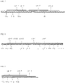
- FIG. 5 is a side view additionally showing only plate cores and a first coil layer in FIG. 4.
- FIG. 6 is a side view additionally showing only plate cores and a first coil layer and a second coil layer in FIG. 4 .
- FIG. 7 is a side view taken along line A-A' shown in FIG. 4 , viewed from a direction of arrow a.
- FIG. 8 is a side view of A-A' shown in FIG. 4 , viewed from a direction of arrow b.
- FIG. 9 is a side view taken along line B-B' shown in FIG. 4 , viewed from a direction of an arrow.
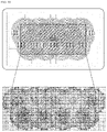
- FIG. 10 shows exemplary power transmission efficiency in a charging area formed on a wireless charging device.
- a wireless charging system 100 may include a wireless charging device 1 that supplies power wirelessly based on an external power source, and a battery device 2 that receives power supplied by the wireless charging device 1.
- the wireless charging device 1 may be connected to an external power source, and may include a plate core and a plurality of transmitting coils Tcs that are disposed above the plate cores and are overlapped with one another.
- the external power source may include any voltage source to supply a voltage having a predetermined magnitude, and may be, for example, a commercial alternating current (AC) power source used at home.
- the wireless charging device 1 may further include an additional cable.
- the battery device 2 may include a receiving coil Rc, a battery, and a micro controller unit (MCU) that controls the receiving coil Rc and the battery, and may be, for example, a mobile device such as a smart phone or a tablet.
- MCU micro controller unit
- the wireless charging device 1 may supply power to the battery device 2 using an electromagnetic induction phenomenon between the transmitting coil Tc and a receiving coil Rc, and the battery device 2 may receive the power from the wireless charging device 1 to charge the battery.
- the battery device 2 is placed on or is close to the wireless charging device 1 so that the receiving coil Rc in the battery device 2 and the transmitting coil Rc in the wireless charging device 1 are located within a predetermined distance.
- magnetic coupling may be performed between the transmitting coil Tc and the receiving coil Rc.
- a magnetic field may be generated in the transmitting coil Tc.
- the current may be induced in the receiving coil Rc based on the magnetic field generated by the transmitting coil Tc.
- the battery device 2 may charge the battery by converting the current induced in the receiving coil Rc into a voltage suitable for the battery.
- a wireless charging device 1 included in the above-mentioned wireless charging system 100 may provide a wide charging area and may simultaneously the plurality of battery devices 2.
- the wireless charging device is described in detail below.
- the wireless charging device 1 includes a substrate 20 and a case 30.
- the two plate cores and a plurality of transmitting coils Tcs are provided on the substrate 20.
- the substrate 20 and the case 30 are coupled to each other to close an inside of the wireless charging device 1.
- a control circuit may be placed on the substrate 20 to apply a current to the plurality of transmitting coils Tcs based on the external power source. Examples of the circuit may include a printed circuit board (PCB), an integrated circuit (IC), and the like.
- the wireless charging device 1 a structure of two plate cores and the plurality of transmitting coils Tcs placed on the substrate 20 is described below in detail. Meanwhile, a description of all coils other than the receiving coil Rc may be regarded as relating to the transmitting coil Tc.
- the wireless charging device 1 may include plate cores and transmitting coils Tcs provided on the plate cores.
- the plate core may include a first plate core 10a and a second plate core 10b.
- the transmitting coil Tc may include a first coil layer to a fourth coil layer.
- FIG. 2 shows the wireless charging device 1, and components of the wireless charging device 1 are not limited to examples shown in FIG. 2 , and some components may be added, changed, or deleted as necessary.
- an x-axis direction is referred to as "a right-side direction” and a -x-axis direction is referred to as “a left-side direction” and an y-axis direction is referred to as “a forward direction” and a -y axis direction is referred to as “a rearward direction” and a z-axis direction is referred to as "an upward direction”, and an -z-axis direction is referred to as "a downward direction”.
- the first plate core 10a and the second plate core 10b may include a component having high permeability and that is not easily broken.
- the first plate core 10a and the second plate core 10b may be made of amorphous metal such as cobalt (Co), iron (Fe), nickel (Ni), boron (B), silicon (Si), or a combination thereof, and may have a sheet shape or a thin film shape.
- the first plate core 10a and the second plate core 10b may be a ferrite core.
- the first plate core 10a and the second plate core 10b may increase magnetic flux density of the magnetic field generated by the transmitting coil Tc, and may efficiently define a magnetic path of the magnetic field.
- the first plate core 10a and the second plate core 10b have the same size and shape and may be spaced apart from each other on the substrate 20. In some examples, as shown in FIG. 2 , the first plate core 10a and the second plate core 10b may be spaced apart from each other by a predetermined distance in a planar direction (e.g., y-axis direction).
- a planar direction e.g., y-axis direction
- the transmitting coil Tc is a flat coil provided above the first plate core 10a and the second plate core 10b and may be wound clockwise or counterclockwise. Such coils may have a circular shape, an oval shape or a square shape. Connection terminals may be provided at both ends of transmitting coil Tc to electrically connect with the control circuit disposed on the substrate 20, and the control circuit may apply the current to each of transmitting coils Tcs to generate the magnetic field.
- the transmitting coil Tc may be divided into the first coil layer to the fourth coil layer according to the arrangement thereof.
- the first coil layer may refer to one or more coils disposed on the plate core to form a single layer
- the second coil layer may refer to one or more coils disposed on the first coil to form a single layer
- a third coil layer may refer to one or more coils disposed on the second coil layer to form a single layer
- a fourth coil layer may refer to one or more coils disposed on the third coil layer to form a single layer.
- the transmitting coil Tc included in the wireless charging device 1 may be elliptical shape having a vertical length of the transmitting coil Tc being greater than a horizontal length of the transmitting coil Tc.
- a vertical outer radius (Roh) and a horizontal outer radius (Rov) of the transmitting coil Tc may be 24.5 mm and 22 mm, respectively, to form a charging area CA (described below with reference to FIG. 10 ) having a width of 10 m and a length of 4 cm, and the charging area is formed in the wireless charging device 1.
- a vertical inner radius (Riv) of the transmitting coil Tc and a horizontal inner radius (Rih) of the transmitting coil Tc may be 10.5 mm and 8.5 mm, respectively.
- the transmitting coil Tc may be coupled to the receiving coil Rc with a predetermined coupling coefficient based on an amount of transmitted power, and the transmitting coil Tc may have predetermined inductance to have the coupling coefficient.
- the number of turns of the transmitting coil Tc is determined based on the inductance of the transmitting coil Tc.
- the transmitting coil Tc may be wound with the number of turns of about 12 to 15 so that the transmitting coil Tc has the inductance of 10.5 [uH] to 11.5 [uH].
- Sizes and shapes of transmitting coils Tcs included in the wireless charging device 1 may vary according to design needs. Sizes and shapes of the transmitting coils Tcs are assumed to be the same.
- the first coil layer may include a 1-1 coil c1-1 and a 1-2 coil c1-2.
- the 1-1 coil c1-1 may be disposed on the first plate core 10a and the 1-2 coil c1-2 may be disposed on the second plate core 10b.
- some or all of the 1-1 coil c1-1 may be disposed on the first plate core 10a and may contact the first plate core 10a and some or all of the 1-2 coil c1-2 may be disposed on the second plate core 10b and may contact the second plate core 10b.
- the 1-1 coil c1-1 when viewed from the top of the wireless charging device 1, the 1-1 coil c1-1 may be included in the first plate core 10a and a portion of the 1-1 coil c1-1 may be included in the first plate core 10a.
- the 1-1 coil c1-1 and the 1-2 coil c1-2 provided as described above may be spaced apart from each other on the same plane.
- the 1-1 coil c1-1 and the 1-2 coil c1-2 may be disposed on a single layer on which the first coil layer is disposed and may be horizontally spaced apart from each other.
- a separation distance between the first plate core 10a and the second plate core 10b may be greater than a separation distance between the 1-1 coil c-1 and the 1-2 coil c1-2.
- the first plate core 10a and the second plate core 10b may be horizontally spaced apart each other by distance d.
- the 1-1 coil cl-1 may be disposed on the first plate core 10a, and a portion of the 1-1 coil c1-1 may protrude toward an outside of the first plate core 10a.
- the 1-2 coil c1-2 may be disposed on the second plate core 10b, and a portion of the 1-2 coil c1-2 may protrude toward an outside of the second plate core 10b.
- the 1-1 coil c1-1 and 1-2 coil c1-2 may be horizontally spaced apart from each other by the distance of dl, and separation distance d1 between the two coils c1-1 and c1-2 may be less than separation distance d between the two plate cores 10a and 10b.
- the separation distance d1 may be determined within a range being greater than 0 and less than d.
- the second coil layer is disposed above the first coil layer and may include a 2-1 coil c2-1 partially overlapped with the 1-1 coil c1-1, a 2-2 coil c2-2 partially overlapped with the 1-1 coil c1-1 and the 1-2 coil c1-2, and a 2-3 coil c2-3 partially overlapped with the 1-2 coil c1-2.
- a portion of the 2-1 coil c2-1 may be disposed on the 1-1 coil c1-1 so that the 2-1 coil c2-1 is partially overlapped with the 1-1 coil c1-1 and a portion of the 2-2 coil c2-2 may be disposed on the 1-1 coil c1-1 and the 1-2 coil cl-2 so that the 2-2 coil c2-2 is partially overlapped with the 1-1 coil c1-1 and the 1-2 coil c1-2, and a portion of the 2-3 coil c2-3 may be disposed on the 1-2 coil c1-2 so that the 2-3 coil c2-3 is partially overlapped with the 1-2 coil c1-2.
- the 2-1 coil c2-1 to the 2-3 coil c2-3 provided as described above may be placed on the same plane and may be spaced apart from one another.
- the 2-1 coil c2-1 to the 2-3 coil c2-3 may be horizontally spaced apart from one another in a single layer on which the second coil layer is disposed.
- the separation distance between the 2-1 coil c2-1 and the 2-2 coil c2-2 may be identical to the separation distance between the 2-2 coil c2-2 and the 2-3 coil c2-3.
- the 2-1 coil c2-1 to the 2-3 coil c2-3 may be arranged on the same horizontal plane by equal distances.
- the second coil layer may be disposed above the first coil layer and may be a single layer and may be collinear.
- centers of coils c2-1, c2-2, and c2-3 may be on the same horizontal line.
- coils c2-1, c2-2, and c2-3 included in the second coil layer may be spaced apart from one another by distance d2.
- An insulating sheet IS may be provided on a first coil layer on a surface where the first coil layer and the second coil layer overlap with each other.
- an upper surface of the first coil layer may contact a lower surface of the insulating sheet IS and a lower surface of the second coil layer may contact an upper surface of the insulating sheet IS.
- the insulating sheet IS may be provided on the first coil layer to insulate the first coil layer and the second coil layer.
- the insulating sheet IS may be provided over the entire first coil layer, or may be selectively provided in an area where the first coil layer and the second coil layer overlap with each other, as shown in the figures.
- the insulating sheet IS may also be provided on a surface where the second coil layer is overlapped with the third coil layer described below and a surface where the third coil layer is overlapped with a fourth coil layer described below. That is, according to the present disclosure, the insulating sheets Iss may be provided on all surfaces where a plurality of coils are overlapped with one another, and the plurality of coils are disposed on respective layers.
- the transmitting coil Tc is basically insulated, insulation performance may be maintained even when any transmitting coil Tc contacts with another transmitting coil Tc.
- an upper surface of one or a first transmitting coil of the plurality of transmitting coils Tcs may contact a lower surface of the insulating sheet IS and a lower surface of another or a second transmitting coil of the plurality of transmitting coils Tcs may contact an upper surface of the insulating sheet IS, thereby providing insulating between transmitting coils Tcs.
- the third coil layer is disposed above the second coil layer and may include a 3-1 coil c3-1 partially overlapped with the 2-1 c2-1 and the 2-2 coil 2-2, and a 3-2 coil c3-2 partially overlapped with the 2-2 coil c2-2 and the 2-3 coil c2-3.
- a portion of the 3-1 coil c3-1 may be disposed above the 2-1 coil c2-1 and the 2-2 coil c2-2 to partially overlap with the 2-1 coil c2-1 and the 2-2 coil c2-2 and a portion of the 3-2 coil c3-2 may be disposed on the 2-2 coil c2-2 and the 2-3 coil c2-3 to partially overlap with the 2-2 coil c2-2 and the 2-3 coil c2-3.
- the 3-1 coil c3-1 and the 3-2 coil c3-2 disposed as described above may be placed on the same plane and may be spaced apart from each other.
- the 3-1 coil c3-1 and the 3-2 coil c3-2 may be disposed on a single layer on which the third coil layer is disposed and may be horizontally spaced apart from each other.
- a fourth coil layer is disposed on the third coil layer, and may include a 4-1 coil c4-1 partially overlapped with the 3-1 coil c3-1 and a 4-2 coil c4-2 partially overlapped with the 3-1 coil c3-1 and the 3-2 coil c3-2.
- a portion of the 4-1 coil c4-1 may be disposed on the 3-1 coil to partially overlap with the 3-1 coil c3-1 and a portion of the 4-2 coil c4-2 may be disposed on the 3-2 coil c3-2 to partially overlap with the 3-2 coil c3-2.
- the 4-1 coil c4-1 and the 4-2 coil c4-2 disposed as described above may be placed on the same plane and may be spaced apart from each other.
- the 4-1 coil c4-1 and the 4-2 coil c4-2 may be disposed on the single layer on which the fourth coil layer is disposed and may be horizontally spaced apart from each other.
- the plurality of coils to form respective layers may be disposed in areas formed by the first plate core 10a and the second plate core 10b.
- An area formed by the first plate core 10a and the second plate core 10b may refer to a single minimum area including the first plate core 10a and the second plate core 10b viewed from the top of the wireless charging device 1.
- an area formed by the first plate core 10a and the second plate core 10b may refer to a rectangular area and the rectangular area may have a lateral length determined by adding a separation distance between two plate cores to a sum of lateral lengths of the two plate cores 10a and 10b and may have a vertical length being identical to a vertical length of each of the two plate cores 10a and 10b.
- a total of nine transmission coils Tcs included in the first coil layer to the fourth coil layer may be disposed in an area formed by the first plate core 10a and the second plate core10b.
- the first plate core 10a and the second plate core 10b may increase the magnetic flux density of the magnetic field generated by any one transmitting coil Tc, among the first coil layer to the fourth coil layer, and efficiently define a magnetic path of the magnetic field.
- the first coil layer and the second coil layer may be disposed on a first horizontal line HL1, and the third coil layer and the fourth coil layer may be disposed on a second horizontal line HL2.
- centers of the 1-1 coil c1-1, the 1-2 coil c1-2, the 2-1 coil c2-1, and the 2-3 coil c2-3 may be disposed on the first horizontal line HL1 and centers of the 3-1 coil c3-1, the 3-2 coil c3-2, the 4-1 coil c4-1, and the 4-2 coil c4-2 may be disposed on the second horizontal line HL2 parallel to the first horizontal line HL1.
- the first horizontal line HL1 and the second horizontal line HL2 may be spaced apart by a predetermined vertical distance dh. Accordingly, the first layer and the second coil layers disposed on the first horizontal line, and the third layer and the fourth coil layers disposed on the second horizontal line may be spaced apart from each other in a y-axis direction by the predetermined vertical distance dh.
- the distance dh between the first horizontal line HL1 and the second horizontal line HL2 may be arbitrarily determined according to design needs. However, as described below in FIG. 10 , the distance dh between the first horizontal line HL1 and the second horizontal line HL2 may be set as 30% to 45% of the vertical length of each of coils to form a charging area CA formed in the wireless charging device 1 having a width of 10 cm and a length of 4 cm.
- the vertical length of each of coils may be 49 mm.
- the distance dh between the first horizontal line HL1 and the second horizontal line HL2 may be set to 17.14mm to 22.05 mm, which comprises 35% to 45% of 49 mm.
- the first coil layer and the second coil layer may be symmetrical with respect to the center vertical line VL of each of the first plate core 10a and the second plate core 10b.
- the center vertical line VL of the first plate core 10a and the second plate core 10b is used to divide the two plate cores 10a and 10b, and may vertically cross a separation portion between the two plate cores 10a and 10b to divide the separation portion in half.
- the center vertical line VL of each of the first plate core 10a and the second plate core 10b may be located between the two plate cores 10a and 10b.
- the center vertical line VL is used to divide the two plate cores 10a and 10b, when the separation distance between the two plate cores 10a and 10b is d, a horizontal distance between the central vertical line VL and the first plate core 10a and a horizontal distance between the central vertical line VL and the second plate core 10b may be the same, for example, may correspond to distance d/2.
- the 1-1 coil c1-1 and the 1-2 coil c1-2 may be symmetrically with respect to the center vertical line VL.
- the distance between the center of the 1-1 coil c1-1 and the center vertical line VL may be equal to the distance between the center of the 1-2 coil c1-2 and the center vertical line VL.
- the 2-1 coil c2-1 and the 2-3 coil c2-3 may be symmetrical to each other with respect to the center vertical line VL.
- the 2-2 coil c2-2 itself may be symmetrical with respect to the center vertical line VL.
- a distance between the center of the 2-1 coil c2-1 and the center vertical line VL may be identical to a distance between the center of the 2-3 coil c2-3 and the center vertical line VL.
- the center of the 2-2 coil c2-2 may be disposed on the center vertical line VL, so that the 2-2 coil c2-2 itself is symmetrical with respect to the center vertical line VL.
- the 3-1 coil c3-1 and the 4-2 coil c4-2 may be symmetrical to each other with respect to the center vertical line VL of the first plate core 10a and the second plate core 10b.
- the layer in which the 3-1 coil c3-1 is disposed may be different from the layer in which the 4-2 coil c4-2 id disposed.
- the 3-1 coil c3-1 and the 4-2 coil c4-2 may be disposed relative to each other so that the distance between the center vertical line VL and the center of the 3-1 coil c3-1 is identical to the distance between the central vertical line VL and the center of the 4-2 coil c4-2.
- the layer in which the 3-2 coil c3-2 is disposed may be different from the layer in which the 4-1 coil c4-1 is disposed.
- the 3-2 coil c3-2 and the 4-1 coil c4-1 may be disposed relative to each other so that a distance dy4 between the central vertical line VL and the center of the 3-2 coil c3-2 is identical to a distance dy4 between the center vertical line VL and a center of the 4-1 coil c4-1, when viewed from the top of the wireless charging device 1
- the distance dy3 between the center of the 4-1 coil c4-1 and the center of the 3-1 coil c3-1, the distance dy3 between the center of the 3-1 coil c3-1 and the center of the 4-2 coil c4-2, and the distance dy3 between the center of the 4-2 coil c4-2 and the center of the 3-2 coil may all be the same.
- the fourth coil layer may overlap with the third coil layer.
- the centers of the 4-1 coil c4-1, the 3-1 coil c3-1, the 4-2 coil c4-2, and the 3-2 coil c3-2, arranged from the left side, may have equal distances dy3.
- the third coil layer and the fourth coil layer are located on different layers from each other, but, viewed from the top of the wireless charging device 1, the third coil layer and the fourth coil layer, which are horizontally and sequentially disposed, may be disposed so that the distance dy3 between the center of the 4-1 coil c4-1 and the center of the 3-1 coil c3-1, the distance dy3 between the center of the 3-1 coil c3-1 and the center of the 4-2 coil c4-2 and the distance dy3 between the center of the 4-2 coil c4-2 and the center of the 3-2 coil c3-2 may be all the same.
- the distance dy3 between the center of the 4-1 coil c4-1 and the center of the 3-1 coil c3-1, the distance dy3 between the center of the 3-1 coil c3-1 and the center of the 4-2 coil c4-2 and the distance dy3 between the center of the 4-2 coil c4-2 and the center of the 3-2 coil c3-2 may be arbitrarily determined according to design needs.
- the distance dy3 between each coil of the fourth coil layer and each coil of the third coil layer may be set as 55 to 65% of the horizontal length of each of coils to provide a charging area CA having a width of 10 cm and a length of 4 cm, formed in the wireless charging device 1.
- the horizontal length of each of coils may be 44 mm.
- the distance dy3 between the center of the 4-1 coil c4-1 and the center of the 3-1 coil c3-1, the distance dy3 between the center of the 3-1 coil c3-1 and the center of the 4-2 coil c4-2 and the distance dy3 between the center of the 4-2 coil c4-2 and the center of the 3-2 coil c3-2 may be set to 24.2 mm to 28. 6 mm, which corresponds to 55% to 65% of 44 mm.
- first coil layer to the fourth coil layer are disposed on different layers from each other, heights of the first coil layer to the fourth coil layer, above the first plate core 10a and the second plate core 10b, may be different from one another. In this case, deviation of the inductance for each coil looking into the receiving coil Rc may be increased, and the deviation between the magnetic flux densities of the magnetic fields generated by coils may be increased, thereby reducing the power transmission efficiency.
- a plurality of height compensating cores may be disposed on the first plate core 10a and the second plate core 10b to compensate for height differences between the first coil layer and the second coil layer, the second coil layer and the third coil layer, and the third coil layer and the fourth coil layer.
- the plurality of height compensating cores may be disposed above the first plate core 10a and the second plate core 10b to compensate for a high difference between the first coil layer and the second coil layer, a height difference between the second coil layer and the third coil layer, and a height difference between the third coil layer and the fourth coil layer.
- the plurality of height compensating cores may include a first height compensating core 11a, a second height compensating core 11b, and a third height compensating core 11c
- the first height compensating core 11a compensates for the height difference between the first coil layer and the second coil layer
- the second height compensating core 11b compensates for the height difference between the second coil layer and the third coil layer
- the third height compensating coil 11c compensates for the height difference between the third coil layer and the fourth coil layer.
- the first height compensating core 11a may be disposed on the first plate core 10a and the second plate core 10b and may be disposed at both sides of the first coil layer and may have the same height as the first coil layer, to compensate for the height difference between the first coil layer and the second coil layer.
- Each of areas of the first plate core 10a and the second plate core 10b may be greater than the area of each of the 1-1 coil c1-1 and the 1-2 coil c1-2, and the first height compensating core 11a may be disposed at both sides of the 1-1 coil c1-1 and the 1-2 coil c1-2 (along the x-axis direction) and may have the same height as the first coil layer.
- the first height compensating core 11a may be disposed on the first plate core 10a in the -x axis direction with respect to the 1-1 coil c1-1. Further, the first height compensating core 11a may be disposed on the second plate core 10b in the + x-axis direction with respect to the 1-2 coil c1-2. Accordingly, a portion of the 2-1 coil c2-1 and a portion of the 2-3 coil c2-3 may be disposed on the first height compensating core 11a.
- the second height compensating core 11b may be disposed at a front end or a rear end of the second coil layer and may have the same height of the second coil layer to compensate for the height difference between the second coil layer and the third coil layer.
- the second height compensating core 11b may be disposed at the front end of the 2-1 to 2-3 coils c2-1 to c2-3 (in the +y direction) and may have the same height as the second coil layer.
- the second height compensating core 11b may be disposed above the first plate core 10a and the first height compensating core 11a in the + y-axis direction with respect to the 2-1 coil c2-1. Further, the second height compensating core 11b may be disposed above the second plate core 10b and the first height compensating core 11a along the + y-axis direction with respect to the 2-3 coil c2-3. Accordingly, a portion of each of the 3-1 coil c3-1 and the 3-2 coil c3-2 may be disposed on the second height compensating core 11b.
- the third height compensating core 11c may be disposed at one end of the third coil layer to have the same height as the third coil layer, to compensate for the height difference between the third coil layer and the fourth coil layer.
- the third height compensating core 11c may be disposed at one side of the 3-1 coil c3-1 (along the -x-axis direction) and may have the same height as the third coil layer. Accordingly, a portion of the 4-1 coil c4-1 may be disposed on the third height compensating core 11c.
- each coil may have equivalent level of inductance regardless of position of coils.
- the power transmission efficiency in the charging area CA formed in the wireless charging device 1 is described below with reference to FIG. 10 .
- a rectangular charging area CA having a width of 10 cm and a length of 4 cm may be formed on the wireless charging device.
- the power transmission efficiency was 40% or more in the entire charging area CA, and in particular, the power transmission efficiency of about 70% is measured in the portion where the coils are provided.
- the wireless charging device 1 may apply the current to any one transmitting coil Tc adjacent to the battery device 2, among coils (e.g., the 1-1 coil, the 2-1 coil, the 2-2 coil, the 3-1 coil, and the 4-1 coil) disposed above the first plate core 10a and may supply the power to the battery device 2.
- coils e.g., the 1-1 coil, the 2-1 coil, the 2-2 coil, the 3-1 coil, and the 4-1 coil
- the wireless charging device 1 may apply the current to any one transmitting coil adjacent to the battery device 2, among coils (e.g., the 1-2 coil, the 2-2 coil, the 2-3 coil, the 3-2 coil, and the 4-2 coil) disposed above the second plate core 10b and may supply the power to the battery device 2.
- coils e.g., the 1-2 coil, the 2-2 coil, the 2-3 coil, the 3-2 coil, and the 4-2 coil
- the wireless charging device 1 may simultaneously apply the current to a portion of coils disposed above the first plate core 10a and a portion of coils disposed above the second plate core 10b to supply the power.
- the magnetic field generated by one core may be prevented from being interfering with the other core by overlapping multiple coils on separated cores, and wireless power transmission using the electromagnetic induction phenomenon may be performed over a wide range.
- the wide charging area may be provided to charge the battery device, so that the battery device is charged without precisely positioning the battery device above the wireless charging device, thereby improving user convenience.
- the multi-wireless charging with respect to the plurality of battery devices is performed, so that a single user may charge a plurality of battery devices at the same time, or a plurality of users may charge their own battery devices at the same time, thereby improving the use efficiency.
Landscapes
- Engineering & Computer Science (AREA)
- Power Engineering (AREA)
- Computer Networks & Wireless Communication (AREA)
- Signal Processing (AREA)
- Charge And Discharge Circuits For Batteries Or The Like (AREA)
Description
- The present disclosure relates to a wireless charging device comprising multiple coils overlapped with one another on separated cores.
- Batteries may receive power from external chargers and may store the power, and may supply the stored power as a power source to operate electronic devices.
- One of methods for charging batteries may include a method for supplying terminals. The method for supplying the terminals may include receiving commercial power and converting commercial power into voltage and current suitable for batteries, and supplying power to batteries through charging terminals.
- However, such a method for supplying the terminals may cause a momentary discharge phenomenon, sparks, fire due to potential difference between charging terminals of batteries and power supply terminals of commercial power sources. Accordingly, wireless charging methods using wireless power transmission have been proposed.
- Wireless charging methods may be performed by non-contact power transmitting devices and non-contact power receiving devices. In the wireless charging methods, power may be transferred from the non-contact power transmitting device to the non-contact power receiving device through an electromagnetic induction phenomenon between the two devices.
- However, through the wireless charging method, one non-contact power transmitting device may supply power only to a single non-contact power receiving device, and the non-contact power receiving device may be placed at a particular position of the non-contact power transmitting device for magnetic coupling between the non-contact power transmitting device and the non-contact power receiving device, thereby having a very narrow chargeable physical range.
- In order to solve the latter problem, the prior art document (
Korean Patent No. 10-0976163 - According to the prior art document, in order to supply power stably even when the non-contact power receiving device moves partially on the non-contact power transmitting device, a primary core provided in the non-contact power transmitting device may include two different types of cores, and the two cores are partially overlap with each other, to form a multi-layer structure.
-
US 2016/020639 A1 relates to a system for simultaneously wirelessly charging portable rechargeable devices, which comprises at least one of a wall mountable and integrable electric switch and socket assembly, wherein the assembly comprises a rear panel comprising at least one of a switch socket outlet and display, a front panel comprising a wireless charging unit and a structurally adaptable coupling member for coupling the front panel to the rear panel, at least a portable computing and communications device removably positioned on the wireless charging unit and a wireless speaker subsystem, wherein the display is wirelessly coupled to the portable computing and communications device. -
US 2018/090956 A1 relates to a wireless charging device including a housing having a charging surface and first and second walls that define an interior cavity, a transmitter coil arrangement disposed within the interior cavity, an interconnection structure positioned within the interior cavity below the transmitter coil arrangement, the interconnection structure including a plurality of packaged electrical components mounted on the interconnection structure and configured to operate the plurality of transmitter coils during wireless power transfer, where the plurality of packaged electrical components is located below the transmitter coil arrangement, and a frame comprising a plurality of openings positioned corresponding to the plurality of packaged electrical components, each opening providing space within which a respective packaged electrical device is disposed. -
US 2018/269716 A1 relates to a transmission device for a wireless charger, which comprises a plurality of planar coils which transmit a wireless power signal for wireless charging and which are arranged so as to be at least partially overlapped with each other, a shielding sheet which has an attachment surface to which a part or all of the planar coils are fixed by the medium of an adhesive layer and which shields a magnetic field generated from the planar coils, and a height deviation compensation means which is provided on the attachment surface and which compensates for individual height deviation between each planar coil and the attachment surface. - However, according to the above-described prior art document, magnetic field interference may occur due to overlapped cores, and power may not be simultaneously supplied to a plurality of non-contact power receiving devices.
- The present disclosure provides a wireless charging device in which multiple coils are overlapped with one another on separated cores.
- The present disclosure also provides a wireless charging device that may provide a wide charging area to charge battery devices.
- The present disclosure further provides a wireless charging device capable of performing multiple-wireless charging for a plurality of battery devices.
- The objects of the present disclosure are not limited to the above-mentioned objects, and other objects and advantages of the present disclosure which are not mentioned may be understood by the following description and more clearly understood by the embodiments of the present disclosure. It will also be readily apparent that the objects and the advantages of the present disclosure may be implemented by features described in claims and a combination thereof.
- According to the present disclosure, a wireless charging device may include two plate cores spaced apart from each other, and a first coil layer to a fourth coil layer that are placed above the two plate cores, placed on different layers from one another, and are overlapped with one another.
- Further, according to the present disclosure, a plurality of coils are disposed above the two plate cores and are widely overlapped with one another in a horizontal direction and a vertical direction, thereby providing a wide charging area in which battery devices are charged.
- Further, according to the present disclosure, in some cases, where the plurality of battery devices are each located above a plurality of plate cores, power may be supplied to the battery device through coils disposed on plate cores, thereby performing multiple-wireless charging with respect to the plurality of battery devices.
- According to the present disclosure, multiple coils are overlapped with one another on separate cores, thereby preventing magnetic fields generated by one core from being interfering with other cores, and performing the wireless power transmission using an electromagnetic induction phenomenon over a wide range.
- Further, according to the present disclosure, the wide charging area may be provided to charge battery devices, so that battery devices may be charged without precisely placing, by the user, the battery device onto the wireless charging device, thereby improving user convenience.
- Further, according to the present disclosure, the multiple-wireless charging may be performed with respect to the plurality of battery devices, so that a single user may simultaneously charge the plurality of battery devices or a plurality of users may simultaneously charge battery devices of users, thereby improving efficiency in using devices.
- A specific effect of the present disclosure, further to the above-mentioned effect, is described together while describing specific matters to implement the present disclosure.
-
-
FIG. 1 shows an exemplary wireless charging system including a wireless charging device. -
FIG. 2 shows an internal structure of the wireless charging device inFIG. 1 . -
FIG. 3 additionally shows a unit coil inFIG. 2 . -
FIG. 4 is a top view showing the wireless charging device inFIG. 2 . -
FIG. 5 is a side view additionally showing only plate cores and a first coil layer inFIG. 4 . -
FIG. 6 is a side view additionally showing only plate cores and a first coil layer and a second coil layer inFIG. 4 . -
FIG. 7 is a side view taken along line AA' shown inFIG. 4 , viewed from a direction of arrow a. -
FIG. 8 is a side view taken along line AA' shown inFIG. 4 , viewed from a direction of arrow b. -
FIG. 9 is a side view taken along line BB' shown inFIG. 4 , viewed in a direction of an arrow. -
FIG. 10 shows power transmission efficiency in a charging area formed on a wireless charging device according to the present disclosure. - The above-mentioned objects, features, and advantages of the present disclosure are described in detail with reference to the accompanying drawings. Accordingly, the skilled person in the art to which the present disclosure pertains may easily implement the technical idea of the present disclosure. In the description of the present disclosure, if it is determined that a detailed description of a well-known relevant technology of the present disclosure may unnecessarily obscure the gist of the present disclosure, the detailed description thereof is omitted. One or more embodiments of the present disclosure are described in detail with reference to the accompanying drawings. In the drawings, same reference numerals are used to refer to same or similar components.
- It will be understood that, although the terms "first", "second", and the like may be used herein to describe various components, however, these components should not be limited by these terms. These terms are only used to distinguish one component from another component. Thus, a first component may be a second component unless otherwise stated.
- Hereinafter, when any component is arranged in "an upper portion (or a lower portion)" of the component or "on (or under") of the component, any component may be arranged in contact with an upper surface (or a lower surface) of the component, and another component may be interposed between the component and any component arranged on (or under) the component.
- Further, when one component is described as being "connected", "coupled", or "connected" to another component, the component may be directly connected or able to be connected to the other component; however, it is also to be understood that an additional component may be "interposed" between the two components, or the two components may be "connected", "coupled" or "connected" through an additional component.
- Unless otherwise stated, each component may be singular or plural throughout the disclosure.
- As used herein, the singular forms "a," "an" and "the" are intended to include the plural forms as well, unless the context clearly indicates otherwise. In the present disclosure, it should not be construed that terms such as "including" or "comprising" necessarily include various types of components or various steps described in the present disclosure, and it should be construed terms such as "including" or "comprising" do not include some components or some steps or may include additional components or steps.
- In the present disclosure, unless otherwise stated, "A and/or B" means A, B or A and B. Unless otherwise stated, "C to D" means "C or more and D or less".
- The present disclosure relates to a wireless charging device in which multiple coils are overlapped with one another on separated cores.
- A wireless charging device according to an embodiment of the present disclosure is described below in detail with reference to
FIGS. 1 to 10 . -
FIG. 1 shows an exemplary wireless charging system including a wireless charging device. -
FIG. 2 shows an internal structure of the wireless charging device inFIG. 1 .FIG. 3 additionally shows a unit coil inFIG. 2 .FIG. 4 is a top view showing the wireless charging device inFIG. 2 . -
FIG. 5 is a side view additionally showing only plate cores and a first coil layer inFIG. 4. FIG. 6 is a side view additionally showing only plate cores and a first coil layer and a second coil layer inFIG. 4 . -
FIG. 7 is a side view taken along line A-A' shown inFIG. 4 , viewed from a direction of arrow a.FIG. 8 is a side view of A-A' shown inFIG. 4 , viewed from a direction of arrow b.FIG. 9 is a side view taken along line B-B' shown inFIG. 4 , viewed from a direction of an arrow. -
FIG. 10 shows exemplary power transmission efficiency in a charging area formed on a wireless charging device. - Referring to
FIG. 1 , awireless charging system 100 may include awireless charging device 1 that supplies power wirelessly based on an external power source, and abattery device 2 that receives power supplied by thewireless charging device 1. - To this end, the
wireless charging device 1 may be connected to an external power source, and may include a plate core and a plurality of transmitting coils Tcs that are disposed above the plate cores and are overlapped with one another. The external power source may include any voltage source to supply a voltage having a predetermined magnitude, and may be, for example, a commercial alternating current (AC) power source used at home. In order to connect with the external power source, thewireless charging device 1 may further include an additional cable. - Meanwhile, the
battery device 2 may include a receiving coil Rc, a battery, and a micro controller unit (MCU) that controls the receiving coil Rc and the battery, and may be, for example, a mobile device such as a smart phone or a tablet. - The
wireless charging device 1 may supply power to thebattery device 2 using an electromagnetic induction phenomenon between the transmitting coil Tc and a receiving coil Rc, and thebattery device 2 may receive the power from thewireless charging device 1 to charge the battery. - In some examples, the
battery device 2 is placed on or is close to thewireless charging device 1 so that the receiving coil Rc in thebattery device 2 and the transmitting coil Rc in thewireless charging device 1 are located within a predetermined distance. - In some cases, where the
wireless charging device 1 applying a current to the transmitting coil Tc based on an external power source, magnetic coupling may be performed between the transmitting coil Tc and the receiving coil Rc. In other words, based on a current flowing through the transmitting coil Tc, a magnetic field may be generated in the transmitting coil Tc. The current may be induced in the receiving coil Rc based on the magnetic field generated by the transmitting coil Tc. Thebattery device 2 may charge the battery by converting the current induced in the receiving coil Rc into a voltage suitable for the battery. - A
wireless charging device 1 included in the above-mentionedwireless charging system 100 may provide a wide charging area and may simultaneously the plurality ofbattery devices 2. The wireless charging device is described in detail below. - Referring back to
FIG. 1 , thewireless charging device 1 includes asubstrate 20 and acase 30. The two plate cores and a plurality of transmitting coils Tcs are provided on thesubstrate 20. Thesubstrate 20 and thecase 30 are coupled to each other to close an inside of thewireless charging device 1. A control circuit may be placed on thesubstrate 20 to apply a current to the plurality of transmitting coils Tcs based on the external power source. Examples of the circuit may include a printed circuit board (PCB), an integrated circuit (IC), and the like. - Among configurations of the
wireless charging device 1, a structure of two plate cores and the plurality of transmitting coils Tcs placed on thesubstrate 20 is described below in detail. Meanwhile, a description of all coils other than the receiving coil Rc may be regarded as relating to the transmitting coil Tc. - Referring to
FIG. 2 , according to an embodiment of the present disclosure, thewireless charging device 1 may include plate cores and transmitting coils Tcs provided on the plate cores. The plate core may include afirst plate core 10a and asecond plate core 10b. The transmitting coil Tc may include a first coil layer to a fourth coil layer. In one embodiment,FIG. 2 shows thewireless charging device 1, and components of thewireless charging device 1 are not limited to examples shown inFIG. 2 , and some components may be added, changed, or deleted as necessary. - In order to explain structural features of the present disclosure, an x-axis direction is referred to as "a right-side direction" and a -x-axis direction is referred to as "a left-side direction" and an y-axis direction is referred to as "a forward direction" and a -y axis direction is referred to as "a rearward direction" and a z-axis direction is referred to as "an upward direction", and an -z-axis direction is referred to as "a downward direction".
- The
first plate core 10a and thesecond plate core 10b may include a component having high permeability and that is not easily broken. In some examples, thefirst plate core 10a and thesecond plate core 10b may be made of amorphous metal such as cobalt (Co), iron (Fe), nickel (Ni), boron (B), silicon (Si), or a combination thereof, and may have a sheet shape or a thin film shape. For example, according to the present disclosure, thefirst plate core 10a and thesecond plate core 10b may be a ferrite core. - Accordingly, the
first plate core 10a and thesecond plate core 10b may increase magnetic flux density of the magnetic field generated by the transmitting coil Tc, and may efficiently define a magnetic path of the magnetic field. - The
first plate core 10a and thesecond plate core 10b have the same size and shape and may be spaced apart from each other on thesubstrate 20. In some examples, as shown inFIG. 2 , thefirst plate core 10a and thesecond plate core 10b may be spaced apart from each other by a predetermined distance in a planar direction (e.g., y-axis direction). - The transmitting coil Tc is a flat coil provided above the
first plate core 10a and thesecond plate core 10b and may be wound clockwise or counterclockwise. Such coils may have a circular shape, an oval shape or a square shape. Connection terminals may be provided at both ends of transmitting coil Tc to electrically connect with the control circuit disposed on thesubstrate 20, and the control circuit may apply the current to each of transmitting coils Tcs to generate the magnetic field. - The transmitting coil Tc may be divided into the first coil layer to the fourth coil layer according to the arrangement thereof. In some examples, the first coil layer may refer to one or more coils disposed on the plate core to form a single layer, and the second coil layer may refer to one or more coils disposed on the first coil to form a single layer, and a third coil layer may refer to one or more coils disposed on the second coil layer to form a single layer, and a fourth coil layer may refer to one or more coils disposed on the third coil layer to form a single layer.
- Referring to
FIG. 3 , the transmitting coil Tc included in thewireless charging device 1 may be elliptical shape having a vertical length of the transmitting coil Tc being greater than a horizontal length of the transmitting coil Tc. For example, a vertical outer radius (Roh) and a horizontal outer radius (Rov) of the transmitting coil Tc may be 24.5 mm and 22 mm, respectively, to form a charging area CA (described below with reference toFIG. 10 ) having a width of 10 m and a length of 4 cm, and the charging area is formed in thewireless charging device 1. A vertical inner radius (Riv) of the transmitting coil Tc and a horizontal inner radius (Rih) of the transmitting coil Tc may be 10.5 mm and 8.5 mm, respectively. - The transmitting coil Tc may be coupled to the receiving coil Rc with a predetermined coupling coefficient based on an amount of transmitted power, and the transmitting coil Tc may have predetermined inductance to have the coupling coefficient. The number of turns of the transmitting coil Tc is determined based on the inductance of the transmitting coil Tc. For example, according to the present disclosure, the transmitting coil Tc may be wound with the number of turns of about 12 to 15 so that the transmitting coil Tc has the inductance of 10.5 [uH] to 11.5 [uH].
- Sizes and shapes of transmitting coils Tcs included in the
wireless charging device 1 may vary according to design needs. Sizes and shapes of the transmitting coils Tcs are assumed to be the same. - The first coil layer may include a 1-1 coil c1-1 and a 1-2 coil c1-2. The 1-1 coil c1-1 may be disposed on the
first plate core 10a and the 1-2 coil c1-2 may be disposed on thesecond plate core 10b. - In some examples, some or all of the 1-1 coil c1-1 may be disposed on the
first plate core 10a and may contact thefirst plate core 10a and some or all of the 1-2 coil c1-2 may be disposed on thesecond plate core 10b and may contact thesecond plate core 10b. For example, when viewed from the top of thewireless charging device 1, the 1-1 coil c1-1 may be included in thefirst plate core 10a and a portion of the 1-1 coil c1-1 may be included in thefirst plate core 10a. - The 1-1 coil c1-1 and the 1-2 coil c1-2 provided as described above may be spaced apart from each other on the same plane. In other words, the 1-1 coil c1-1 and the 1-2 coil c1-2 may be disposed on a single layer on which the first coil layer is disposed and may be horizontally spaced apart from each other.
- In this case, a separation distance between the
first plate core 10a and thesecond plate core 10b may be greater than a separation distance between the 1-1 coil c-1 and the 1-2 coil c1-2. - Referring to
FIGS. 4 and 5 , thefirst plate core 10a and thesecond plate core 10b may be horizontally spaced apart each other by distance d. The 1-1 coil cl-1 may be disposed on thefirst plate core 10a, and a portion of the 1-1 coil c1-1 may protrude toward an outside of thefirst plate core 10a. The 1-2 coil c1-2 may be disposed on thesecond plate core 10b, and a portion of the 1-2 coil c1-2 may protrude toward an outside of thesecond plate core 10b. - At this time, the 1-1 coil c1-1 and 1-2 coil c1-2 may be horizontally spaced apart from each other by the distance of dl, and separation distance d1 between the two coils c1-1 and c1-2 may be less than separation distance d between the two
plate cores - The second coil layer is disposed above the first coil layer and may include a 2-1 coil c2-1 partially overlapped with the 1-1 coil c1-1, a 2-2 coil c2-2 partially overlapped with the 1-1 coil c1-1 and the 1-2 coil c1-2, and a 2-3 coil c2-3 partially overlapped with the 1-2 coil c1-2.
- In some examples, a portion of the 2-1 coil c2-1 may be disposed on the 1-1 coil c1-1 so that the 2-1 coil c2-1 is partially overlapped with the 1-1 coil c1-1 and a portion of the 2-2 coil c2-2 may be disposed on the 1-1 coil c1-1 and the 1-2 coil cl-2 so that the 2-2 coil c2-2 is partially overlapped with the 1-1 coil c1-1 and the 1-2 coil c1-2, and a portion of the 2-3 coil c2-3 may be disposed on the 1-2 coil c1-2 so that the 2-3 coil c2-3 is partially overlapped with the 1-2 coil c1-2.
- The 2-1 coil c2-1 to the 2-3 coil c2-3 provided as described above may be placed on the same plane and may be spaced apart from one another. In other words, the 2-1 coil c2-1 to the 2-3 coil c2-3 may be horizontally spaced apart from one another in a single layer on which the second coil layer is disposed.
- At this time, the separation distance between the 2-1 coil c2-1 and the 2-2 coil c2-2 may be identical to the separation distance between the 2-2 coil c2-2 and the 2-3 coil c2-3. In other words, the 2-1 coil c2-1 to the 2-3 coil c2-3 may be arranged on the same horizontal plane by equal distances.
- Referring to
FIG. 6 , the second coil layer may be disposed above the first coil layer and may be a single layer and may be collinear. In other words, in the second coil layer, centers of coils c2-1, c2-2, and c2-3 may be on the same horizontal line. In this case, coils c2-1, c2-2, and c2-3 included in the second coil layer may be spaced apart from one another by distance d2. - An insulating sheet IS may be provided on a first coil layer on a surface where the first coil layer and the second coil layer overlap with each other. In other words, an upper surface of the first coil layer may contact a lower surface of the insulating sheet IS and a lower surface of the second coil layer may contact an upper surface of the insulating sheet IS.
- Referring back to
FIG. 6 , the insulating sheet IS may be provided on the first coil layer to insulate the first coil layer and the second coil layer. The insulating sheet IS may be provided over the entire first coil layer, or may be selectively provided in an area where the first coil layer and the second coil layer overlap with each other, as shown in the figures. - The insulating sheet IS may also be provided on a surface where the second coil layer is overlapped with the third coil layer described below and a surface where the third coil layer is overlapped with a fourth coil layer described below. That is, according to the present disclosure, the insulating sheets Iss may be provided on all surfaces where a plurality of coils are overlapped with one another, and the plurality of coils are disposed on respective layers.
- As the transmitting coil Tc is basically insulated, insulation performance may be maintained even when any transmitting coil Tc contacts with another transmitting coil Tc. However, even when current leakage occurs due to external damage or the like of the transmitting coil Tc, an upper surface of one or a first transmitting coil of the plurality of transmitting coils Tcs may contact a lower surface of the insulating sheet IS and a lower surface of another or a second transmitting coil of the plurality of transmitting coils Tcs may contact an upper surface of the insulating sheet IS, thereby providing insulating between transmitting coils Tcs. The third coil layer is disposed above the second coil layer and may include a 3-1 coil c3-1 partially overlapped with the 2-1 c2-1 and the 2-2 coil 2-2, and a 3-2 coil c3-2 partially overlapped with the 2-2 coil c2-2 and the 2-3 coil c2-3.
- In some examples, a portion of the 3-1 coil c3-1 may be disposed above the 2-1 coil c2-1 and the 2-2 coil c2-2 to partially overlap with the 2-1 coil c2-1 and the 2-2 coil c2-2 and a portion of the 3-2 coil c3-2 may be disposed on the 2-2 coil c2-2 and the 2-3 coil c2-3 to partially overlap with the 2-2 coil c2-2 and the 2-3 coil c2-3.
- The 3-1 coil c3-1 and the 3-2 coil c3-2 disposed as described above may be placed on the same plane and may be spaced apart from each other. In other words, the 3-1 coil c3-1 and the 3-2 coil c3-2 may be disposed on a single layer on which the third coil layer is disposed and may be horizontally spaced apart from each other.
- A fourth coil layer is disposed on the third coil layer, and may include a 4-1 coil c4-1 partially overlapped with the 3-1 coil c3-1 and a 4-2 coil c4-2 partially overlapped with the 3-1 coil c3-1 and the 3-2 coil c3-2.
- In some examples, a portion of the 4-1 coil c4-1 may be disposed on the 3-1 coil to partially overlap with the 3-1 coil c3-1 and a portion of the 4-2 coil c4-2 may be disposed on the 3-2 coil c3-2 to partially overlap with the 3-2 coil c3-2.
- The 4-1 coil c4-1 and the 4-2 coil c4-2 disposed as described above may be placed on the same plane and may be spaced apart from each other. In other words, the 4-1 coil c4-1 and the 4-2 coil c4-2 may be disposed on the single layer on which the fourth coil layer is disposed and may be horizontally spaced apart from each other.
- The plurality of coils to form respective layers may be disposed in areas formed by the
first plate core 10a and thesecond plate core 10b. - An area formed by the
first plate core 10a and thesecond plate core 10b may refer to a single minimum area including thefirst plate core 10a and thesecond plate core 10b viewed from the top of thewireless charging device 1. - Accordingly, as shown in
FIG. 4 , an area formed by thefirst plate core 10a and thesecond plate core 10b may refer to a rectangular area and the rectangular area may have a lateral length determined by adding a separation distance between two plate cores to a sum of lateral lengths of the twoplate cores plate cores - In this case, as shown in
FIG. 4 , a total of nine transmission coils Tcs included in the first coil layer to the fourth coil layer may be disposed in an area formed by thefirst plate core 10a and the second plate core10b. - Accordingly, the
first plate core 10a and thesecond plate core 10b may increase the magnetic flux density of the magnetic field generated by any one transmitting coil Tc, among the first coil layer to the fourth coil layer, and efficiently define a magnetic path of the magnetic field. - Referring back to
FIG. 4 , the first coil layer and the second coil layer may be disposed on a first horizontal line HL1, and the third coil layer and the fourth coil layer may be disposed on a second horizontal line HL2. - In some examples, centers of the 1-1 coil c1-1, the 1-2 coil c1-2, the 2-1 coil c2-1, and the 2-3 coil c2-3 may be disposed on the first horizontal line HL1 and centers of the 3-1 coil c3-1, the 3-2 coil c3-2, the 4-1 coil c4-1, and the 4-2 coil c4-2 may be disposed on the second horizontal line HL2 parallel to the first horizontal line HL1.
- The first horizontal line HL1 and the second horizontal line HL2 may be spaced apart by a predetermined vertical distance dh. Accordingly, the first layer and the second coil layers disposed on the first horizontal line, and the third layer and the fourth coil layers disposed on the second horizontal line may be spaced apart from each other in a y-axis direction by the predetermined vertical distance dh.
- The distance dh between the first horizontal line HL1 and the second horizontal line HL2 may be arbitrarily determined according to design needs. However, as described below in
FIG. 10 , the distance dh between the first horizontal line HL1 and the second horizontal line HL2 may be set as 30% to 45% of the vertical length of each of coils to form a charging area CA formed in thewireless charging device 1 having a width of 10 cm and a length of 4 cm. - For example, as described with reference to
FIG. 3 , in some cases, where the vertical outer radius Roh of each coil is 24.5 mm, the vertical length of each of coils may be 49 mm. In this case, the distance dh between the first horizontal line HL1 and the second horizontal line HL2 may be set to 17.14mm to 22.05 mm, which comprises 35% to 45% of 49 mm. - The first coil layer and the second coil layer may be symmetrical with respect to the center vertical line VL of each of the
first plate core 10a and thesecond plate core 10b. The center vertical line VL of thefirst plate core 10a and thesecond plate core 10b is used to divide the twoplate cores plate cores - Referring back to
FIG. 4 , the center vertical line VL of each of thefirst plate core 10a and thesecond plate core 10b may be located between the twoplate cores plate cores plate cores first plate core 10a and a horizontal distance between the central vertical line VL and thesecond plate core 10b may be the same, for example, may correspond to distance d/2. - The 1-1 coil c1-1 and the 1-2 coil c1-2 may be symmetrically with respect to the center vertical line VL. In other words, the distance between the center of the 1-1 coil c1-1 and the center vertical line VL may be equal to the distance between the center of the 1-2 coil c1-2 and the center vertical line VL.
- Further, the 2-1 coil c2-1 and the 2-3 coil c2-3 may be symmetrical to each other with respect to the center vertical line VL. The 2-2 coil c2-2 itself may be symmetrical with respect to the center vertical line VL. In other words, a distance between the center of the 2-1 coil c2-1 and the center vertical line VL may be identical to a distance between the center of the 2-3 coil c2-3 and the center vertical line VL. Meanwhile, the center of the 2-2 coil c2-2 may be disposed on the center vertical line VL, so that the 2-2 coil c2-2 itself is symmetrical with respect to the center vertical line VL.
- The 3-1 coil c3-1 and the 4-2 coil c4-2 may be symmetrical to each other with respect to the center vertical line VL of the
first plate core 10a and thesecond plate core 10b. - In some examples, the layer in which the 3-1 coil c3-1 is disposed may be different from the layer in which the 4-2 coil c4-2 id disposed. When viewed from the top of the
wireless charging device 1, the 3-1 coil c3-1 and the 4-2 coil c4-2 may be disposed relative to each other so that the distance between the center vertical line VL and the center of the 3-1 coil c3-1 is identical to the distance between the central vertical line VL and the center of the 4-2 coil c4-2. - Further, the 3-2 coil c3-2 and the 4-1 coil c4-1 may be symmetrical to each other with respect to the center vertical line VL of each of the
first plate core 10a and thesecond plate core 10b. - Similarly, the layer in which the 3-2 coil c3-2 is disposed may be different from the layer in which the 4-1 coil c4-1 is disposed. The 3-2 coil c3-2 and the 4-1 coil c4-1 may be disposed relative to each other so that a distance dy4 between the central vertical line VL and the center of the 3-2 coil c3-2 is identical to a distance dy4 between the center vertical line VL and a center of the 4-1 coil c4-1, when viewed from the top of the
wireless charging device 1 - In some cases, where the third coil layer and the fourth coil layer are disposed through the above-described method, the distance dy3 between the center of the 4-1 coil c4-1 and the center of the 3-1 coil c3-1, the distance dy3 between the center of the 3-1 coil c3-1 and the center of the 4-2 coil c4-2, and the distance dy3 between the center of the 4-2 coil c4-2 and the center of the 3-2 coil may all be the same.
- As shown in
FIG. 4 , the fourth coil layer may overlap with the third coil layer. At this time, the centers of the 4-1 coil c4-1, the 3-1 coil c3-1, the 4-2 coil c4-2, and the 3-2 coil c3-2, arranged from the left side, may have equal distances dy3. In some examples, the third coil layer and the fourth coil layer are located on different layers from each other, but, viewed from the top of thewireless charging device 1, the third coil layer and the fourth coil layer, which are horizontally and sequentially disposed, may be disposed so that the distance dy3 between the center of the 4-1 coil c4-1 and the center of the 3-1 coil c3-1, the distance dy3 between the center of the 3-1 coil c3-1 and the center of the 4-2 coil c4-2 and the distance dy3 between the center of the 4-2 coil c4-2 and the center of the 3-2 coil c3-2 may be all the same. - The distance dy3 between the center of the 4-1 coil c4-1 and the center of the 3-1 coil c3-1, the distance dy3 between the center of the 3-1 coil c3-1 and the center of the 4-2 coil c4-2 and the distance dy3 between the center of the 4-2 coil c4-2 and the center of the 3-2 coil c3-2 may be arbitrarily determined according to design needs. However, as described below in
FIG. 10 , the distance dy3 between each coil of the fourth coil layer and each coil of the third coil layer may be set as 55 to 65% of the horizontal length of each of coils to provide a charging area CA having a width of 10 cm and a length of 4 cm, formed in thewireless charging device 1. - For example, as described with reference to
FIG. 3 , based on the horizontal outer radius Rov of each of coils being 22 mm, the horizontal length of each of coils may be 44 mm. At this time, the distance dy3 between the center of the 4-1 coil c4-1 and the center of the 3-1 coil c3-1, the distance dy3 between the center of the 3-1 coil c3-1 and the center of the 4-2 coil c4-2 and the distance dy3 between the center of the 4-2 coil c4-2 and the center of the 3-2 coil c3-2 may be set to 24.2 mm to 28. 6 mm, which corresponds to 55% to 65% of 44 mm. - As the first coil layer to the fourth coil layer are disposed on different layers from each other, heights of the first coil layer to the fourth coil layer, above the
first plate core 10a and thesecond plate core 10b, may be different from one another. In this case, deviation of the inductance for each coil looking into the receiving coil Rc may be increased, and the deviation between the magnetic flux densities of the magnetic fields generated by coils may be increased, thereby reducing the power transmission efficiency. - In order to prevent the above configuration, a plurality of height compensating cores may be disposed on the
first plate core 10a and thesecond plate core 10b to compensate for height differences between the first coil layer and the second coil layer, the second coil layer and the third coil layer, and the third coil layer and the fourth coil layer. - Referring back to
FIG. 2 , the plurality of height compensating cores may be disposed above thefirst plate core 10a and thesecond plate core 10b to compensate for a high difference between the first coil layer and the second coil layer, a height difference between the second coil layer and the third coil layer, and a height difference between the third coil layer and the fourth coil layer. - In more detail, with reference to
FIGS. 2 and7 to 9 , the plurality of height compensating cores may include a firstheight compensating core 11a, a secondheight compensating core 11b, and a thirdheight compensating core 11c, and the firstheight compensating core 11a compensates for the height difference between the first coil layer and the second coil layer and the secondheight compensating core 11b compensates for the height difference between the second coil layer and the third coil layer, and the thirdheight compensating coil 11c compensates for the height difference between the third coil layer and the fourth coil layer. - The first
height compensating core 11a may be disposed on thefirst plate core 10a and thesecond plate core 10b and may be disposed at both sides of the first coil layer and may have the same height as the first coil layer, to compensate for the height difference between the first coil layer and the second coil layer. - Each of areas of the
first plate core 10a and thesecond plate core 10b may be greater than the area of each of the 1-1 coil c1-1 and the 1-2 coil c1-2, and the firstheight compensating core 11a may be disposed at both sides of the 1-1 coil c1-1 and the 1-2 coil c1-2 (along the x-axis direction) and may have the same height as the first coil layer. - In some examples, the first
height compensating core 11a may be disposed on thefirst plate core 10a in the -x axis direction with respect to the 1-1 coil c1-1. Further, the firstheight compensating core 11a may be disposed on thesecond plate core 10b in the + x-axis direction with respect to the 1-2 coil c1-2. Accordingly, a portion of the 2-1 coil c2-1 and a portion of the 2-3 coil c2-3 may be disposed on the firstheight compensating core 11a. - The second
height compensating core 11b may be disposed at a front end or a rear end of the second coil layer and may have the same height of the second coil layer to compensate for the height difference between the second coil layer and the third coil layer. For example, the secondheight compensating core 11b may be disposed at the front end of the 2-1 to 2-3 coils c2-1 to c2-3 (in the +y direction) and may have the same height as the second coil layer. - In some examples, the second
height compensating core 11b may be disposed above thefirst plate core 10a and the firstheight compensating core 11a in the + y-axis direction with respect to the 2-1 coil c2-1. Further, the secondheight compensating core 11b may be disposed above thesecond plate core 10b and the firstheight compensating core 11a along the + y-axis direction with respect to the 2-3 coil c2-3. Accordingly, a portion of each of the 3-1 coil c3-1 and the 3-2 coil c3-2 may be disposed on the secondheight compensating core 11b. - The third
height compensating core 11c may be disposed at one end of the third coil layer to have the same height as the third coil layer, to compensate for the height difference between the third coil layer and the fourth coil layer. - In some examples, the third
height compensating core 11c may be disposed at one side of the 3-1 coil c3-1 (along the -x-axis direction) and may have the same height as the third coil layer. Accordingly, a portion of the 4-1 coil c4-1 may be disposed on the thirdheight compensating core 11c. - As the height compensating cores are provided between the first coil layer to the fourth coil layer to compensate for the height differences between the coils disposed in respective layers, each coil may have equivalent level of inductance regardless of position of coils.
- The power transmission efficiency in the charging area CA formed in the
wireless charging device 1 is described below with reference toFIG. 10 . - Referring to
FIG. 10 , as thewireless charging device 1 has the above-described structure, a rectangular charging area CA having a width of 10 cm and a length of 4 cm may be formed on the wireless charging device. - Based on a result of measurement of the power transmission efficiency, the power transmission efficiency was 40% or more in the entire charging area CA, and in particular, the power transmission efficiency of about 70% is measured in the portion where the coils are provided.
- In some cases, where the
battery device 2 is disposed above thefirst plate core 10a of thewireless charging device 1, thewireless charging device 1 may apply the current to any one transmitting coil Tc adjacent to thebattery device 2, among coils (e.g., the 1-1 coil, the 2-1 coil, the 2-2 coil, the 3-1 coil, and the 4-1 coil) disposed above thefirst plate core 10a and may supply the power to thebattery device 2. By contrast, in some cases, where thebattery device 2 is located above thesecond plate core 10b, thewireless charging device 1 may apply the current to any one transmitting coil adjacent to thebattery device 2, among coils (e.g., the 1-2 coil, the 2-2 coil, the 2-3 coil, the 3-2 coil, and the 4-2 coil) disposed above thesecond plate core 10b and may supply the power to thebattery device 2. - Further, in some cases, where the two
battery devices 2 are located above thefirst plate core 10a and thesecond plate core 10b, respectively, thewireless charging device 1 may simultaneously apply the current to a portion of coils disposed above thefirst plate core 10a and a portion of coils disposed above thesecond plate core 10b to supply the power. - According to the present disclosure, the magnetic field generated by one core may be prevented from being interfering with the other core by overlapping multiple coils on separated cores, and wireless power transmission using the electromagnetic induction phenomenon may be performed over a wide range.
- Further, according to the present disclosure, the wide charging area may be provided to charge the battery device, so that the battery device is charged without precisely positioning the battery device above the wireless charging device, thereby improving user convenience.
- Further, according to the present disclosure, the multi-wireless charging with respect to the plurality of battery devices is performed, so that a single user may charge a plurality of battery devices at the same time, or a plurality of users may charge their own battery devices at the same time, thereby improving the use efficiency.
- Various substitutions, modifications, and changes can be made within the scope that does not deviate from the technical idea of the present disclosure for the skilled person in the art to which the present disclosure pertains, the above-mentioned disclosure is not limited to the above-mentioned embodiment and the accompanying drawings.
- Other embodiments are within the scope of the following claims.
Claims (13)
- A wireless charging device, comprising:a first plate core (10a) and a second plate core (10b) spaced apart from each other;a first coil layer comprising a 1-1 coil (c1-1) disposed on the first plate core (10a) and a 1-2 coil (c1-2) disposed on the second plate core (10b); anda second coil layer disposed above the first coil layer, the second coil layer comprising a 2-1 coil (c2-1) partially overlapped with the 1-1 coil (c1-1), a 2-2 coil (c2-2) partially overlapped with at least one of the 1-1 coil (c1-1) and the 1-2 coil (c1-2), and a 2-3 coil (c2-3) partially overlapped with the 1-2 coil (c1-2); characterised in that it further comprisesa third coil layer disposed above the second coil layer, the third coil layer comprising a 3-1 coil (c3-1) partially overlapped with at least one of the 2-1 coil (c2-1) and the 2-2 coil (c2-2), and a 3-2 coil (c3-2) partially overlapped with at least one of the 2-2 coil (c2-2) and the 2-3 coil (c2-3); anda fourth coil layer disposed above the third coil layer and comprising a 4-1 coil (c4-1) partially overlapped with the 3-1 coil (c3-1) and a 4-2 coil (c4-2) partially overlapped with at least one of the 3-1 coil (c3-1) and the 3-2 coil (c3-2),wherein the 3-1 coil (c3-1) and the 4-2 coil (c4-2) are disposed symmetrical to each other with respect to a center vertical line (VL) between the first plate core (10a) and the second plate core (10b),wherein the 3-2 coil (c3-2) and the 4-1 coil (c4-1) are disposed symmetrical to each other with respect to the center vertical line (VL) between the first plate core (10a) and the second plate core (10b),wherein an area where the 3-1 coil (c3-1), the 3-2 coil (c3-2) and the second plate core (10b) overlap is larger than an area where the 3-1 coil (c3-1), the 3-2 coil (c3-2) and the first plate core (10a) overlap, andwherein an area where the 4-1 coil (c4-1), the 4-2 coil (c4-2) and the first plate core (10a) overlap is larger than an area where the 4-1 coil (c4-1), the 4-2 coil (c4-2) and the second plate core (10b) overlap.
- The wireless charging device of claim 1, wherein the plurality of coils in at least one of the first, second, third and fourth coil layers are placed on a same plane and spaced apart from one another.
- The wireless charging device of claim 1 or 2, wherein a separation distance between the 2-1 coil (c2-1) and the 2-2 coil (c2-2) is the same as a separation distance between the 2-2 coil (c2-2) and the 2-3 coil (c2-3).
- The wireless charging device of any one of the preceding claims, wherein some of the coils in the second, third and fourth coil layers are disposed above a separation area formed between the first plate core (10a) and the second plate core (10b).
- The wireless charging device of any one of the preceding claims,wherein the first coil layer and the second coil layer are disposed on a first horizontal line (HL1), andwherein the third coil layer and the fourth coil layer are disposed on a second horizontal line (HL2) different from the first horizontal line (HL1).
- The wireless charging device of claim 5, wherein a distance between the first horizontal line (HL1) and the second horizontal line (HL2) corresponds to approximately 35% to 45% of a vertical length of one of the coils in one of the first to fourth coil layers.
- The wireless charging device of any one of the preceding claims, wherein a separation distance (d) between the first plate core (10a) and the second plate core (10b) is greater than a separation distance (d1) between the 1-1 coil (c1-1) and the 1-2 coil (c1-2).
- The wireless charging device of any one of the preceding claims, wherein each of the first coil layer and the second coil layer is disposed symmetrically with respect to a center vertical line (VL) between the first plate core (10a) and the second plate core (10b).
- The wireless charging device of any one of the preceding claims, wherein a distance (dy3) between a center of the 4-1 coil (c4-1) and a center of the 3-1 coil (c3-1), a distance (dy3) between a center of the 3-1 coil (c3-1) and a center of the 4-2 coil (c4-2), and a distance (dy3) between a center of the 4-2 coil (c4-2) and a center of the 3-2 coil (c3-2) are substantially the same.
- The wireless charging device of any one of the preceding claims, wherein the distance between the center of the 4-1 coil (c4-1) and the center of the 3-1 coil (c3-1), the distance between the center of the 3-1 coil (c3-1) and the center of the 4-2 coil (c4-2), and the distance between the center of the 4-2 coil (c4-2) and the center of the 3-2 coil (c3-2) corresponds to approximately 55% to 65% of a horizontal length of one of the coils in one of the first to fourth coil layers.
- The wireless charging device of any one of the preceding claims, further comprising:
a plurality of height compensating cores (11a, 11b, 11c) disposed above the first plate core (10a) and the second plate core (10b) to compensate for height differences between the first coil layer and the second coil layer, the second coil layer and the third coil layer, and the third coil layer and the fourth coil layer. - The wireless charging device of claim 11, wherein the plurality of height compensating cores (11a, 11b, 11c) comprise at least two of the following:a first height compensating core (11a) disposed on the first plate core (10a) and the second plate core (10b), disposed at both sides of the first coil layer, and having the same height as the first coil layer to compensate for a height difference between the first coil layer and the second coil layer;a second height compensating core (11b) disposed at a front end or a rear end of the second coil layer, and having the same height as the second coil layer to compensate for a height difference between the second coil layer and the third coil layer; anda third height compensating core (11c) disposed at one side of the third coil layer, and having the same height as the third coil layer to compensate for a height difference between the third coil layer and the fourth coil layer.
- The wireless charging device of any one of the preceding claims, further comprising:
an insulating sheet (IS) provided on a surface where a coil in one of the first to fourth coil layers overlaps a coil in another of the first to fourth coil layers.
Applications Claiming Priority (1)
| Application Number | Priority Date | Filing Date | Title |
|---|---|---|---|
| KR1020180172180A KR102703307B1 (en) | 2018-12-28 | 2018-12-28 | Apparatus for wireless charging using multi-coil |
Publications (2)
| Publication Number | Publication Date |
|---|---|
| EP3675323A1 EP3675323A1 (en) | 2020-07-01 |
| EP3675323B1 true EP3675323B1 (en) | 2022-10-26 |
Family
ID=69055765
Family Applications (1)
| Application Number | Title | Priority Date | Filing Date |
|---|---|---|---|
| EP19219862.0A Active EP3675323B1 (en) | 2018-12-28 | 2019-12-27 | Wireless charging device using multi-coil |
Country Status (3)
| Country | Link |
|---|---|
| US (1) | US11437860B2 (en) |
| EP (1) | EP3675323B1 (en) |
| KR (1) | KR102703307B1 (en) |
Families Citing this family (9)
| Publication number | Priority date | Publication date | Assignee | Title |
|---|---|---|---|---|
| US11482890B2 (en) | 2020-04-30 | 2022-10-25 | Nucurrent, Inc. | Surface mountable wireless power transmitter for transmission at extended range |
| KR102847723B1 (en) * | 2020-09-04 | 2025-08-20 | 삼성전자주식회사 | Wireless power transmission device including shielding member |
| CN112260333B (en) * | 2020-09-17 | 2025-08-05 | 南京睿赫电子有限公司 | Wireless charging device and wireless charging method |
| US11476711B2 (en) | 2020-12-23 | 2022-10-18 | Nucurrent, Inc. | Wireless power transmitters and associated base stations for through-structure charging |
| KR102950410B1 (en) * | 2021-07-16 | 2026-04-10 | 삼성전자주식회사 | Electronic device comprising transmission coil providing wireless power for reception coils |
| US12573886B2 (en) | 2021-07-30 | 2026-03-10 | Aira, Inc. | Laminar coil array in a multi-device wireless charger |
| US11967830B2 (en) * | 2021-10-12 | 2024-04-23 | Nucurrent, Inc. | Wireless power transmitters for transmitting power at extended separation distances with magnetic connectors |
| US12132325B2 (en) | 2021-10-12 | 2024-10-29 | Nucurrent, Inc. | Wireless power transmitter with removable magnetic connector panel |
| US11637448B1 (en) * | 2021-10-12 | 2023-04-25 | Nucurrent, Inc. | Wireless power transmitter with removable magnetic connector panel for vehicular use |
Family Cites Families (18)
| Publication number | Priority date | Publication date | Assignee | Title |
|---|---|---|---|---|
| US3549825A (en) * | 1967-09-18 | 1970-12-22 | Ncr Co | Magnetic transducer with planar spiral coil extending into the gap |
| US8169185B2 (en) * | 2006-01-31 | 2012-05-01 | Mojo Mobility, Inc. | System and method for inductive charging of portable devices |
| US11201500B2 (en) * | 2006-01-31 | 2021-12-14 | Mojo Mobility, Inc. | Efficiencies and flexibilities in inductive (wireless) charging |
| KR101513631B1 (en) | 2008-11-05 | 2015-04-20 | 엘지전자 주식회사 | Charging device for mobile terminal and charging method thereof |
| KR101745735B1 (en) | 2009-04-08 | 2017-06-12 | 액세스 비지니스 그룹 인터내셔날 엘엘씨 | Selectable coil array |
| KR100976163B1 (en) | 2009-06-19 | 2010-08-16 | 정춘길 | Wireless charging system using core structure for wireless power transmission and method using the same |
| KR101777101B1 (en) | 2010-05-31 | 2017-09-11 | 주식회사 한림포스텍 | Devices and Methods for Non-contact Power Transmission |
| US9178369B2 (en) * | 2011-01-18 | 2015-11-03 | Mojo Mobility, Inc. | Systems and methods for providing positioning freedom, and support of different voltages, protocols, and power levels in a wireless power system |
| JP2012244840A (en) * | 2011-05-23 | 2012-12-10 | Asahi Denki Kenkyusho:Kk | Toroidal coil, bobbin coil, air-core coil and winding method thereof |
| US20160020639A1 (en) * | 2014-07-17 | 2016-01-21 | Pavan Pudipeddi | Methods and systems for simultaneously wirelessly charging portable devices using custom-designed and retro-designed power control and supply assemblies and architectural structures facilitating hands-free operation of the portable devices and interaction therewith |
| KR101765692B1 (en) * | 2014-11-07 | 2017-08-07 | 주식회사 아모센스 | transmission device for wireless charging apparatus |
| CN104376955B (en) * | 2014-11-28 | 2016-01-20 | 信源电子制品(昆山)有限公司 | Lattice coil and method, inductor, transformer, wireless charger, relay |
| KR20170054708A (en) | 2015-11-10 | 2017-05-18 | 엘지이노텍 주식회사 | Multi-Coil Wireless Charging Method and Apparatus and System therefor |
| US10601468B2 (en) * | 2016-09-06 | 2020-03-24 | Apple Inc. | Wirelessly charged devices |
| US20180091000A1 (en) * | 2016-09-23 | 2018-03-29 | Apple Inc. | Multi-layer transmitter coil arrangement for wireless charging mats |
| US11271436B2 (en) * | 2017-06-28 | 2022-03-08 | Lg Electronics Inc. | Multi-coil based wireless power transmission device and method |
| JP7043749B2 (en) * | 2017-07-03 | 2022-03-30 | スミダコーポレーション株式会社 | Coil parts |
| CN208489698U (en) * | 2018-07-16 | 2019-02-12 | 成都瑞德星无线技术有限公司 | A kind of wireless charging R-T unit of adaptive power control |
-
2018
- 2018-12-28 KR KR1020180172180A patent/KR102703307B1/en active Active
-
2019
- 2019-12-26 US US16/727,040 patent/US11437860B2/en active Active
- 2019-12-27 EP EP19219862.0A patent/EP3675323B1/en active Active
Also Published As
| Publication number | Publication date |
|---|---|
| KR20200082040A (en) | 2020-07-08 |
| KR102703307B1 (en) | 2024-09-04 |
| US20200212722A1 (en) | 2020-07-02 |
| EP3675323A1 (en) | 2020-07-01 |
| US11437860B2 (en) | 2022-09-06 |
Similar Documents
| Publication | Publication Date | Title |
|---|---|---|
| US11437860B2 (en) | Wireless charging device using multi-coil | |
| US11469621B2 (en) | Wireless charging apparatus using multiple coils and wireless charging system comprising the same | |
| EP1915809B1 (en) | Auxiliary winding for improved performance of a planar inductive charging platform | |
| CN101714788B (en) | Contact-less power transfer device and method | |
| US8772978B2 (en) | Power transmitting apparatus, power receiving apparatus, and wireless power transmission system | |
| KR101765692B1 (en) | transmission device for wireless charging apparatus | |
| CN102882283B (en) | Core assembly for wireless power transmitting device and wireless power transmitting device having same | |
| US10574091B2 (en) | Enclosures for high power wireless power transfer systems | |
| US20110210617A1 (en) | Power transmission across a substantially planar interface by magnetic induction and geometrically-complimentary magnetic field structures | |
| CN111527666B (en) | wireless power transmission device | |
| US20120086394A1 (en) | Battery charging system | |
| US20150054457A1 (en) | Secondary coil of receiver for non-contact charging system | |
| WO2017023080A1 (en) | Wireless power transfer module for vehicles | |
| WO2012027531A1 (en) | Wireless power supply system and multi-layer shim assembly | |
| JP2012010533A (en) | Power transmission system, and power supply device and portable apparatus therefor | |
| KR20130119585A (en) | Wireless power transmitting/receiving apparatus | |
| KR20090098239A (en) | Wireless power transmission device and wireless charging system using same | |
| US20140056462A1 (en) | Electro-acoustic transducer | |
| EP3790162B1 (en) | Wireless charging apparatus for preventing magnetic field cancellation between adjacent coils | |
| CN102005623A (en) | Inductive rechargeable battery | |
| JPH09223520A (en) | Charging device | |
| KR20190111381A (en) | Wireless charging pad and wireless charging apparatus | |
| WO2020096342A1 (en) | Wireless charging pad and wireless charging device | |
| CN108900223A (en) | A kind of portable terminal | |
| KR20200017048A (en) | Wireless charging pad and wireless charging apparatus |
Legal Events
| Date | Code | Title | Description |
|---|---|---|---|
| PUAI | Public reference made under article 153(3) epc to a published international application that has entered the european phase |
Free format text: ORIGINAL CODE: 0009012 |
|
| STAA | Information on the status of an ep patent application or granted ep patent |
Free format text: STATUS: REQUEST FOR EXAMINATION WAS MADE |
|
| 17P | Request for examination filed |
Effective date: 20200127 |
|
| AK | Designated contracting states |
Kind code of ref document: A1 Designated state(s): AL AT BE BG CH CY CZ DE DK EE ES FI FR GB GR HR HU IE IS IT LI LT LU LV MC MK MT NL NO PL PT RO RS SE SI SK SM TR |
|
| AX | Request for extension of the european patent |
Extension state: BA ME |
|
| RBV | Designated contracting states (corrected) |
Designated state(s): AL AT BE BG CH CY CZ DE DK EE ES FI FR GB GR HR HU IE IS IT LI LT LU LV MC MK MT NL NO PL PT RO RS SE SI SK SM TR |
|
| RIN1 | Information on inventor provided before grant (corrected) |
Inventor name: PARK, SOOYONG Inventor name: KIM, HWANYONG Inventor name: CHOI, HYENGCHEUL Inventor name: CHAE, BEOM SEOK Inventor name: LEE, SEONG HUN Inventor name: LEE, EUNSOO Inventor name: KWON, JAESOON |
|
| STAA | Information on the status of an ep patent application or granted ep patent |
Free format text: STATUS: EXAMINATION IS IN PROGRESS |
|
| 17Q | First examination report despatched |
Effective date: 20210527 |
|
| RIC1 | Information provided on ipc code assigned before grant |
Ipc: H01F 27/36 20060101ALI20220223BHEP Ipc: H01F 38/14 20060101ALI20220223BHEP Ipc: H04B 5/00 20060101ALI20220223BHEP Ipc: H02J 50/40 20160101AFI20220223BHEP |
|
| GRAP | Despatch of communication of intention to grant a patent |
Free format text: ORIGINAL CODE: EPIDOSNIGR1 |
|
| STAA | Information on the status of an ep patent application or granted ep patent |
Free format text: STATUS: GRANT OF PATENT IS INTENDED |
|
| INTG | Intention to grant announced |
Effective date: 20220519 |
|
| GRAS | Grant fee paid |
Free format text: ORIGINAL CODE: EPIDOSNIGR3 |
|
| GRAA | (expected) grant |
Free format text: ORIGINAL CODE: 0009210 |
|
| STAA | Information on the status of an ep patent application or granted ep patent |
Free format text: STATUS: THE PATENT HAS BEEN GRANTED |
|
| AK | Designated contracting states |
Kind code of ref document: B1 Designated state(s): AL AT BE BG CH CY CZ DE DK EE ES FI FR GB GR HR HU IE IS IT LI LT LU LV MC MK MT NL NO PL PT RO RS SE SI SK SM TR |
|
| REG | Reference to a national code |
Ref country code: GB Ref legal event code: FG4D |
|
| REG | Reference to a national code |
Ref country code: CH Ref legal event code: EP |
|
| REG | Reference to a national code |
Ref country code: DE Ref legal event code: R096 Ref document number: 602019021072 Country of ref document: DE |
|
| REG | Reference to a national code |
Ref country code: AT Ref legal event code: REF Ref document number: 1527778 Country of ref document: AT Kind code of ref document: T Effective date: 20221115 |
|
| REG | Reference to a national code |
Ref country code: IE Ref legal event code: FG4D |
|
| REG | Reference to a national code |
Ref country code: LT Ref legal event code: MG9D |
|
| REG | Reference to a national code |
Ref country code: NL Ref legal event code: MP Effective date: 20221026 |
|
| REG | Reference to a national code |
Ref country code: AT Ref legal event code: MK05 Ref document number: 1527778 Country of ref document: AT Kind code of ref document: T Effective date: 20221026 |
|
| PG25 | Lapsed in a contracting state [announced via postgrant information from national office to epo] |
Ref country code: NL Free format text: LAPSE BECAUSE OF FAILURE TO SUBMIT A TRANSLATION OF THE DESCRIPTION OR TO PAY THE FEE WITHIN THE PRESCRIBED TIME-LIMIT Effective date: 20221026 |
|
| PG25 | Lapsed in a contracting state [announced via postgrant information from national office to epo] |
Ref country code: SE Free format text: LAPSE BECAUSE OF FAILURE TO SUBMIT A TRANSLATION OF THE DESCRIPTION OR TO PAY THE FEE WITHIN THE PRESCRIBED TIME-LIMIT Effective date: 20221026 Ref country code: PT Free format text: LAPSE BECAUSE OF FAILURE TO SUBMIT A TRANSLATION OF THE DESCRIPTION OR TO PAY THE FEE WITHIN THE PRESCRIBED TIME-LIMIT Effective date: 20230227 Ref country code: NO Free format text: LAPSE BECAUSE OF FAILURE TO SUBMIT A TRANSLATION OF THE DESCRIPTION OR TO PAY THE FEE WITHIN THE PRESCRIBED TIME-LIMIT Effective date: 20230126 Ref country code: LT Free format text: LAPSE BECAUSE OF FAILURE TO SUBMIT A TRANSLATION OF THE DESCRIPTION OR TO PAY THE FEE WITHIN THE PRESCRIBED TIME-LIMIT Effective date: 20221026 Ref country code: FI Free format text: LAPSE BECAUSE OF FAILURE TO SUBMIT A TRANSLATION OF THE DESCRIPTION OR TO PAY THE FEE WITHIN THE PRESCRIBED TIME-LIMIT Effective date: 20221026 Ref country code: ES Free format text: LAPSE BECAUSE OF FAILURE TO SUBMIT A TRANSLATION OF THE DESCRIPTION OR TO PAY THE FEE WITHIN THE PRESCRIBED TIME-LIMIT Effective date: 20221026 Ref country code: AT Free format text: LAPSE BECAUSE OF FAILURE TO SUBMIT A TRANSLATION OF THE DESCRIPTION OR TO PAY THE FEE WITHIN THE PRESCRIBED TIME-LIMIT Effective date: 20221026 |
|
| PG25 | Lapsed in a contracting state [announced via postgrant information from national office to epo] |
Ref country code: RS Free format text: LAPSE BECAUSE OF FAILURE TO SUBMIT A TRANSLATION OF THE DESCRIPTION OR TO PAY THE FEE WITHIN THE PRESCRIBED TIME-LIMIT Effective date: 20221026 Ref country code: PL Free format text: LAPSE BECAUSE OF FAILURE TO SUBMIT A TRANSLATION OF THE DESCRIPTION OR TO PAY THE FEE WITHIN THE PRESCRIBED TIME-LIMIT Effective date: 20221026 Ref country code: LV Free format text: LAPSE BECAUSE OF FAILURE TO SUBMIT A TRANSLATION OF THE DESCRIPTION OR TO PAY THE FEE WITHIN THE PRESCRIBED TIME-LIMIT Effective date: 20221026 Ref country code: IS Free format text: LAPSE BECAUSE OF FAILURE TO SUBMIT A TRANSLATION OF THE DESCRIPTION OR TO PAY THE FEE WITHIN THE PRESCRIBED TIME-LIMIT Effective date: 20230226 Ref country code: HR Free format text: LAPSE BECAUSE OF FAILURE TO SUBMIT A TRANSLATION OF THE DESCRIPTION OR TO PAY THE FEE WITHIN THE PRESCRIBED TIME-LIMIT Effective date: 20221026 |
|
| REG | Reference to a national code |
Ref country code: DE Ref legal event code: R097 Ref document number: 602019021072 Country of ref document: DE |
|
| PG25 | Lapsed in a contracting state [announced via postgrant information from national office to epo] |
Ref country code: SM Free format text: LAPSE BECAUSE OF FAILURE TO SUBMIT A TRANSLATION OF THE DESCRIPTION OR TO PAY THE FEE WITHIN THE PRESCRIBED TIME-LIMIT Effective date: 20221026 Ref country code: RO Free format text: LAPSE BECAUSE OF FAILURE TO SUBMIT A TRANSLATION OF THE DESCRIPTION OR TO PAY THE FEE WITHIN THE PRESCRIBED TIME-LIMIT Effective date: 20221026 Ref country code: EE Free format text: LAPSE BECAUSE OF FAILURE TO SUBMIT A TRANSLATION OF THE DESCRIPTION OR TO PAY THE FEE WITHIN THE PRESCRIBED TIME-LIMIT Effective date: 20221026 Ref country code: DK Free format text: LAPSE BECAUSE OF FAILURE TO SUBMIT A TRANSLATION OF THE DESCRIPTION OR TO PAY THE FEE WITHIN THE PRESCRIBED TIME-LIMIT Effective date: 20221026 Ref country code: CZ Free format text: LAPSE BECAUSE OF FAILURE TO SUBMIT A TRANSLATION OF THE DESCRIPTION OR TO PAY THE FEE WITHIN THE PRESCRIBED TIME-LIMIT Effective date: 20221026 |
|
| REG | Reference to a national code |
Ref country code: CH Ref legal event code: PL |
|
| REG | Reference to a national code |
Ref country code: BE Ref legal event code: MM Effective date: 20221231 |
|
| PG25 | Lapsed in a contracting state [announced via postgrant information from national office to epo] |
Ref country code: SK Free format text: LAPSE BECAUSE OF FAILURE TO SUBMIT A TRANSLATION OF THE DESCRIPTION OR TO PAY THE FEE WITHIN THE PRESCRIBED TIME-LIMIT Effective date: 20221026 Ref country code: LU Free format text: LAPSE BECAUSE OF NON-PAYMENT OF DUE FEES Effective date: 20221227 Ref country code: AL Free format text: LAPSE BECAUSE OF FAILURE TO SUBMIT A TRANSLATION OF THE DESCRIPTION OR TO PAY THE FEE WITHIN THE PRESCRIBED TIME-LIMIT Effective date: 20221026 |
|
| PLBE | No opposition filed within time limit |
Free format text: ORIGINAL CODE: 0009261 |
|
| STAA | Information on the status of an ep patent application or granted ep patent |
Free format text: STATUS: NO OPPOSITION FILED WITHIN TIME LIMIT |
|
| 26N | No opposition filed |
Effective date: 20230727 |
|
| PG25 | Lapsed in a contracting state [announced via postgrant information from national office to epo] |
Ref country code: LI Free format text: LAPSE BECAUSE OF NON-PAYMENT OF DUE FEES Effective date: 20221231 Ref country code: IE Free format text: LAPSE BECAUSE OF NON-PAYMENT OF DUE FEES Effective date: 20221227 Ref country code: CH Free format text: LAPSE BECAUSE OF NON-PAYMENT OF DUE FEES Effective date: 20221231 |
|
| PG25 | Lapsed in a contracting state [announced via postgrant information from national office to epo] |
Ref country code: SI Free format text: LAPSE BECAUSE OF FAILURE TO SUBMIT A TRANSLATION OF THE DESCRIPTION OR TO PAY THE FEE WITHIN THE PRESCRIBED TIME-LIMIT Effective date: 20221026 Ref country code: FR Free format text: LAPSE BECAUSE OF NON-PAYMENT OF DUE FEES Effective date: 20221231 Ref country code: BE Free format text: LAPSE BECAUSE OF NON-PAYMENT OF DUE FEES Effective date: 20221231 |
|
| PG25 | Lapsed in a contracting state [announced via postgrant information from national office to epo] |
Ref country code: HU Free format text: LAPSE BECAUSE OF FAILURE TO SUBMIT A TRANSLATION OF THE DESCRIPTION OR TO PAY THE FEE WITHIN THE PRESCRIBED TIME-LIMIT; INVALID AB INITIO Effective date: 20191227 |
|
| PG25 | Lapsed in a contracting state [announced via postgrant information from national office to epo] |
Ref country code: CY Free format text: LAPSE BECAUSE OF FAILURE TO SUBMIT A TRANSLATION OF THE DESCRIPTION OR TO PAY THE FEE WITHIN THE PRESCRIBED TIME-LIMIT Effective date: 20221026 |
|
| PG25 | Lapsed in a contracting state [announced via postgrant information from national office to epo] |
Ref country code: MK Free format text: LAPSE BECAUSE OF FAILURE TO SUBMIT A TRANSLATION OF THE DESCRIPTION OR TO PAY THE FEE WITHIN THE PRESCRIBED TIME-LIMIT Effective date: 20221026 Ref country code: IT Free format text: LAPSE BECAUSE OF FAILURE TO SUBMIT A TRANSLATION OF THE DESCRIPTION OR TO PAY THE FEE WITHIN THE PRESCRIBED TIME-LIMIT Effective date: 20221026 |
|
| PG25 | Lapsed in a contracting state [announced via postgrant information from national office to epo] |
Ref country code: MC Free format text: LAPSE BECAUSE OF FAILURE TO SUBMIT A TRANSLATION OF THE DESCRIPTION OR TO PAY THE FEE WITHIN THE PRESCRIBED TIME-LIMIT Effective date: 20221026 |
|
| PG25 | Lapsed in a contracting state [announced via postgrant information from national office to epo] |
Ref country code: TR Free format text: LAPSE BECAUSE OF FAILURE TO SUBMIT A TRANSLATION OF THE DESCRIPTION OR TO PAY THE FEE WITHIN THE PRESCRIBED TIME-LIMIT Effective date: 20221026 Ref country code: MC Free format text: LAPSE BECAUSE OF FAILURE TO SUBMIT A TRANSLATION OF THE DESCRIPTION OR TO PAY THE FEE WITHIN THE PRESCRIBED TIME-LIMIT Effective date: 20221026 |
|
| PG25 | Lapsed in a contracting state [announced via postgrant information from national office to epo] |
Ref country code: BG Free format text: LAPSE BECAUSE OF FAILURE TO SUBMIT A TRANSLATION OF THE DESCRIPTION OR TO PAY THE FEE WITHIN THE PRESCRIBED TIME-LIMIT Effective date: 20221026 |
|
| GBPC | Gb: european patent ceased through non-payment of renewal fee |
Effective date: 20231227 |
|
| PG25 | Lapsed in a contracting state [announced via postgrant information from national office to epo] |
Ref country code: MT Free format text: LAPSE BECAUSE OF FAILURE TO SUBMIT A TRANSLATION OF THE DESCRIPTION OR TO PAY THE FEE WITHIN THE PRESCRIBED TIME-LIMIT Effective date: 20221026 |
|
| PG25 | Lapsed in a contracting state [announced via postgrant information from national office to epo] |
Ref country code: GB Free format text: LAPSE BECAUSE OF NON-PAYMENT OF DUE FEES Effective date: 20231227 |
|
| PG25 | Lapsed in a contracting state [announced via postgrant information from national office to epo] |
Ref country code: GB Free format text: LAPSE BECAUSE OF NON-PAYMENT OF DUE FEES Effective date: 20231227 |
|
| PG25 | Lapsed in a contracting state [announced via postgrant information from national office to epo] |
Ref country code: GR Free format text: LAPSE BECAUSE OF NON-PAYMENT OF DUE FEES Effective date: 20221026 |
|
| PG25 | Lapsed in a contracting state [announced via postgrant information from national office to epo] |
Ref country code: GR Free format text: LAPSE BECAUSE OF NON-PAYMENT OF DUE FEES Effective date: 20221026 |
|
| PGFP | Annual fee paid to national office [announced via postgrant information from national office to epo] |
Ref country code: DE Payment date: 20251105 Year of fee payment: 7 |