EP3675097A1 - Electronic device - Google Patents
Electronic device Download PDFInfo
- Publication number
- EP3675097A1 EP3675097A1 EP19213475.7A EP19213475A EP3675097A1 EP 3675097 A1 EP3675097 A1 EP 3675097A1 EP 19213475 A EP19213475 A EP 19213475A EP 3675097 A1 EP3675097 A1 EP 3675097A1
- Authority
- EP
- European Patent Office
- Prior art keywords
- electronic
- elements
- electronic modules
- sensing elements
- electronic device
- Prior art date
- Legal status (The legal status is an assumption and is not a legal conclusion. Google has not performed a legal analysis and makes no representation as to the accuracy of the status listed.)
- Granted
Links
Images






Classifications
-
- G—PHYSICS
- G09—EDUCATION; CRYPTOGRAPHY; DISPLAY; ADVERTISING; SEALS
- G09F—DISPLAYING; ADVERTISING; SIGNS; LABELS OR NAME-PLATES; SEALS
- G09F9/00—Indicating arrangements for variable information in which the information is built-up on a support by selection or combination of individual elements
- G09F9/30—Indicating arrangements for variable information in which the information is built-up on a support by selection or combination of individual elements in which the desired character or characters are formed by combining individual elements
- G09F9/302—Indicating arrangements for variable information in which the information is built-up on a support by selection or combination of individual elements in which the desired character or characters are formed by combining individual elements characterised by the form or geometrical disposition of the individual elements
- G09F9/3026—Video wall, i.e. stackable semiconductor matrix display modules
-
- G—PHYSICS
- G09—EDUCATION; CRYPTOGRAPHY; DISPLAY; ADVERTISING; SEALS
- G09G—ARRANGEMENTS OR CIRCUITS FOR CONTROL OF INDICATING DEVICES USING STATIC MEANS TO PRESENT VARIABLE INFORMATION
- G09G3/00—Control arrangements or circuits, of interest only in connection with visual indicators other than cathode-ray tubes
- G09G3/20—Control arrangements or circuits, of interest only in connection with visual indicators other than cathode-ray tubes for presentation of an assembly of a number of characters, e.g. a page, by composing the assembly by combination of individual elements arranged in a matrix no fixed position being assigned to or needed to be assigned to the individual characters or partial characters
-
- G—PHYSICS
- G09—EDUCATION; CRYPTOGRAPHY; DISPLAY; ADVERTISING; SEALS
- G09G—ARRANGEMENTS OR CIRCUITS FOR CONTROL OF INDICATING DEVICES USING STATIC MEANS TO PRESENT VARIABLE INFORMATION
- G09G3/00—Control arrangements or circuits, of interest only in connection with visual indicators other than cathode-ray tubes
- G09G3/20—Control arrangements or circuits, of interest only in connection with visual indicators other than cathode-ray tubes for presentation of an assembly of a number of characters, e.g. a page, by composing the assembly by combination of individual elements arranged in a matrix no fixed position being assigned to or needed to be assigned to the individual characters or partial characters
- G09G3/22—Control arrangements or circuits, of interest only in connection with visual indicators other than cathode-ray tubes for presentation of an assembly of a number of characters, e.g. a page, by composing the assembly by combination of individual elements arranged in a matrix no fixed position being assigned to or needed to be assigned to the individual characters or partial characters using controlled light sources
- G09G3/30—Control arrangements or circuits, of interest only in connection with visual indicators other than cathode-ray tubes for presentation of an assembly of a number of characters, e.g. a page, by composing the assembly by combination of individual elements arranged in a matrix no fixed position being assigned to or needed to be assigned to the individual characters or partial characters using controlled light sources using electroluminescent panels
- G09G3/32—Control arrangements or circuits, of interest only in connection with visual indicators other than cathode-ray tubes for presentation of an assembly of a number of characters, e.g. a page, by composing the assembly by combination of individual elements arranged in a matrix no fixed position being assigned to or needed to be assigned to the individual characters or partial characters using controlled light sources using electroluminescent panels semiconductive, e.g. using light-emitting diodes [LED]
-
- H—ELECTRICITY
- H10—SEMICONDUCTOR DEVICES; ELECTRIC SOLID-STATE DEVICES NOT OTHERWISE PROVIDED FOR
- H10F—INORGANIC SEMICONDUCTOR DEVICES SENSITIVE TO INFRARED RADIATION, LIGHT, ELECTROMAGNETIC RADIATION OF SHORTER WAVELENGTH OR CORPUSCULAR RADIATION
- H10F30/00—Individual radiation-sensitive semiconductor devices in which radiation controls the flow of current through the devices, e.g. photodetectors
- H10F30/20—Individual radiation-sensitive semiconductor devices in which radiation controls the flow of current through the devices, e.g. photodetectors the devices having potential barriers, e.g. phototransistors
- H10F30/21—Individual radiation-sensitive semiconductor devices in which radiation controls the flow of current through the devices, e.g. photodetectors the devices having potential barriers, e.g. phototransistors the devices being sensitive to infrared, visible or ultraviolet radiation
- H10F30/22—Individual radiation-sensitive semiconductor devices in which radiation controls the flow of current through the devices, e.g. photodetectors the devices having potential barriers, e.g. phototransistors the devices being sensitive to infrared, visible or ultraviolet radiation the devices having only one potential barrier, e.g. photodiodes
- H10F30/223—Individual radiation-sensitive semiconductor devices in which radiation controls the flow of current through the devices, e.g. photodetectors the devices having potential barriers, e.g. phototransistors the devices being sensitive to infrared, visible or ultraviolet radiation the devices having only one potential barrier, e.g. photodiodes the potential barrier being a PIN barrier
-
- H—ELECTRICITY
- H10—SEMICONDUCTOR DEVICES; ELECTRIC SOLID-STATE DEVICES NOT OTHERWISE PROVIDED FOR
- H10F—INORGANIC SEMICONDUCTOR DEVICES SENSITIVE TO INFRARED RADIATION, LIGHT, ELECTROMAGNETIC RADIATION OF SHORTER WAVELENGTH OR CORPUSCULAR RADIATION
- H10F39/00—Integrated devices, or assemblies of multiple devices, comprising at least one element covered by group H10F30/00, e.g. radiation detectors comprising photodiode arrays
- H10F39/10—Integrated devices
- H10F39/103—Integrated devices the at least one element covered by H10F30/00 having potential barriers, e.g. integrated devices comprising photodiodes or phototransistors
-
- H—ELECTRICITY
- H10—SEMICONDUCTOR DEVICES; ELECTRIC SOLID-STATE DEVICES NOT OTHERWISE PROVIDED FOR
- H10F—INORGANIC SEMICONDUCTOR DEVICES SENSITIVE TO INFRARED RADIATION, LIGHT, ELECTROMAGNETIC RADIATION OF SHORTER WAVELENGTH OR CORPUSCULAR RADIATION
- H10F55/00—Radiation-sensitive semiconductor devices covered by groups H10F10/00, H10F19/00 or H10F30/00 being structurally associated with electric light sources and electrically or optically coupled thereto
- H10F55/20—Radiation-sensitive semiconductor devices covered by groups H10F10/00, H10F19/00 or H10F30/00 being structurally associated with electric light sources and electrically or optically coupled thereto wherein the electric light source controls the radiation-sensitive semiconductor devices, e.g. optocouplers
- H10F55/25—Radiation-sensitive semiconductor devices covered by groups H10F10/00, H10F19/00 or H10F30/00 being structurally associated with electric light sources and electrically or optically coupled thereto wherein the electric light source controls the radiation-sensitive semiconductor devices, e.g. optocouplers wherein the radiation-sensitive devices and the electric light source are all semiconductor devices
-
- H—ELECTRICITY
- H10—SEMICONDUCTOR DEVICES; ELECTRIC SOLID-STATE DEVICES NOT OTHERWISE PROVIDED FOR
- H10F—INORGANIC SEMICONDUCTOR DEVICES SENSITIVE TO INFRARED RADIATION, LIGHT, ELECTROMAGNETIC RADIATION OF SHORTER WAVELENGTH OR CORPUSCULAR RADIATION
- H10F77/00—Constructional details of devices covered by this subclass
- H10F77/40—Optical elements or arrangements
- H10F77/413—Optical elements or arrangements directly associated or integrated with the devices, e.g. back reflectors
-
- H—ELECTRICITY
- H10—SEMICONDUCTOR DEVICES; ELECTRIC SOLID-STATE DEVICES NOT OTHERWISE PROVIDED FOR
- H10F—INORGANIC SEMICONDUCTOR DEVICES SENSITIVE TO INFRARED RADIATION, LIGHT, ELECTROMAGNETIC RADIATION OF SHORTER WAVELENGTH OR CORPUSCULAR RADIATION
- H10F77/00—Constructional details of devices covered by this subclass
- H10F77/93—Interconnections
- H10F77/933—Interconnections for devices having potential barriers
-
- H—ELECTRICITY
- H10—SEMICONDUCTOR DEVICES; ELECTRIC SOLID-STATE DEVICES NOT OTHERWISE PROVIDED FOR
- H10F—INORGANIC SEMICONDUCTOR DEVICES SENSITIVE TO INFRARED RADIATION, LIGHT, ELECTROMAGNETIC RADIATION OF SHORTER WAVELENGTH OR CORPUSCULAR RADIATION
- H10F77/00—Constructional details of devices covered by this subclass
- H10F77/95—Circuit arrangements
- H10F77/953—Circuit arrangements for devices having potential barriers
-
- H—ELECTRICITY
- H10—SEMICONDUCTOR DEVICES; ELECTRIC SOLID-STATE DEVICES NOT OTHERWISE PROVIDED FOR
- H10K—ORGANIC ELECTRIC SOLID-STATE DEVICES
- H10K59/00—Integrated devices, or assemblies of multiple devices, comprising at least one organic light-emitting element covered by group H10K50/00
- H10K59/10—OLED displays
- H10K59/18—Tiled displays
-
- H—ELECTRICITY
- H10—SEMICONDUCTOR DEVICES; ELECTRIC SOLID-STATE DEVICES NOT OTHERWISE PROVIDED FOR
- H10W—GENERIC PACKAGES, INTERCONNECTIONS, CONNECTORS OR OTHER CONSTRUCTIONAL DETAILS OF DEVICES COVERED BY CLASS H10
- H10W76/00—Containers; Fillings or auxiliary members therefor; Seals
- H10W76/10—Containers or parts thereof
- H10W76/12—Containers or parts thereof characterised by their shape
- H10W76/13—Containers comprising a conductive base serving as an interconnection
- H10W76/134—Containers comprising a conductive base serving as an interconnection having other interconnections parallel to the conductive base
-
- H—ELECTRICITY
- H10—SEMICONDUCTOR DEVICES; ELECTRIC SOLID-STATE DEVICES NOT OTHERWISE PROVIDED FOR
- H10W—GENERIC PACKAGES, INTERCONNECTIONS, CONNECTORS OR OTHER CONSTRUCTIONAL DETAILS OF DEVICES COVERED BY CLASS H10
- H10W90/00—Package configurations
-
- G—PHYSICS
- G09—EDUCATION; CRYPTOGRAPHY; DISPLAY; ADVERTISING; SEALS
- G09G—ARRANGEMENTS OR CIRCUITS FOR CONTROL OF INDICATING DEVICES USING STATIC MEANS TO PRESENT VARIABLE INFORMATION
- G09G2300/00—Aspects of the constitution of display devices
- G09G2300/02—Composition of display devices
- G09G2300/026—Video wall, i.e. juxtaposition of a plurality of screens to create a display screen of bigger dimensions
-
- G—PHYSICS
- G09—EDUCATION; CRYPTOGRAPHY; DISPLAY; ADVERTISING; SEALS
- G09G—ARRANGEMENTS OR CIRCUITS FOR CONTROL OF INDICATING DEVICES USING STATIC MEANS TO PRESENT VARIABLE INFORMATION
- G09G2320/00—Control of display operating conditions
- G09G2320/02—Improving the quality of display appearance
- G09G2320/0233—Improving the luminance or brightness uniformity across the screen
-
- G—PHYSICS
- G09—EDUCATION; CRYPTOGRAPHY; DISPLAY; ADVERTISING; SEALS
- G09G—ARRANGEMENTS OR CIRCUITS FOR CONTROL OF INDICATING DEVICES USING STATIC MEANS TO PRESENT VARIABLE INFORMATION
- G09G2360/00—Aspects of the architecture of display systems
- G09G2360/14—Detecting light within display terminals, e.g. using a single or a plurality of photosensors
- G09G2360/145—Detecting light within display terminals, e.g. using a single or a plurality of photosensors the light originating from the display screen
Definitions
- the present disclosure relates to an electronic device. More specifically, the present disclosure relates to an electronic device comprising tiled electronic modules.
- the applications of the display devices are not limited to monitors, mobile phones, laptops, televisions, etc.
- tiled display device or tiled display systems are developed to extend the applications of the display devices to video walls, advertising boards, and other electronic devices for displaying large images.
- the tiled display device or the tiled display system may suffer from the problem that the properties of the electronic modules comprised therein are different, resulting in that the whole image displayed thereon is non-uniform.
- the present disclosure provides an electronic device, which comprises: a substrate; a plurality of sensing elements disposed on the substrate; and a plurality of electronic modules disposed on the substrate, each electronic module comprising a plurality of electronic elements, wherein the plurality of electronic modules are arranged in a manner to expose the plurality of sensing elements.
- the present disclosure further provides another electronic device, which comprises: a substrate; a plurality of sensing elements disposed on the substrate; and a plurality of electronic modules disposed on the substrate, each electronic module comprising a plurality of electronic elements, wherein at least two of the electronic modules are sensed by at least one of the sensing elements.
- the present disclosure also provides another electronic device, which comprises: a substrate; a plurality of sensing elements disposed on the substrate; and a plurality of electronic modules disposed on the substrate; wherein at least one of the plurality of electronic modules comprises a plurality of electronic elements, and the plurality of electronic modules are arranged in a manner to expose the plurality of sensing elements.
- connect is intended not only directly connect with other element, but also intended indirectly connect and electrically connect with other element.
- the value when a value is in a range from a first value to a second value, the value can be the first value, the second value, or another value between the first value and the second value.
- the terms “about”, “nearly”, “almost”, “approximately”, or “substantially” are usually expressed within 20% of a given value or range, or within 10%, or within 5%, or within 3%, or within 2%, or within 1%, or within 0.5%.
- the quantity given here is an approximate quantity, that is, in the absence of specific descriptions of "about”, “nearly”, “almost”, “approximately”, or “substantially”, the meaning of "about”, “nearly”, “almost”, “approximately”, or “substantially” may still be implied.
- FIG. 1 is a top view of an electronic device according to one embodiment of the present disclosure.
- the electronic device of the present embodiment comprises: a substrate 11; a plurality of sensing elements 13 disposed on the substrate 11; and a plurality of electronic modules 12 disposed on the substrate 11, wherein each of the electronic modules 12 comprises a plurality of electronic elements 121. In some other embodiments, at least one electronic module 12 comprises a plurality of electronic elements 121.
- the electronic device of the present embodiment may further comprise a controller 14 electrically connected to the substrate 11.
- the controller 14 is electrically connected to the substrate 11 via a circuit board 15.
- the controller 14 can be a timing controller (T-con controller), but the present disclosure is not limited thereto.
- the electronic modules 12 are disposed on the substrate 11 and arranged in juxtaposition to form a tiled electronic device.
- FIG. 1 not all the electronic modules 12 but only four electronic modules 12 are shown. However, the present disclosure is not limited thereto. The number and the arrangement of the electronic modules 12 can be adjusted according to the actual demand.
- each of the electronic modules 12 comprises nine electronic elements 121, but the present disclosure is not limited thereto. The number and the arrangement of the electronic elements 121 can be adjusted according to the actual demand.
- FIG. 2A is a cross-sectional view of the electronic device of the present embodiment along the line I-I' indicated in FIG. 1 .
- the substrate 11 used in the electronic device of the present embodiment is a driving substrate with a circuit layer 111 formed thereon, and the electronic modules 12 are electrically connected to the circuit layer 111 on the substrate 11 through conductive elements 123.
- the electronic modules 12 used in the electronic device of the present embodiment may respectively comprise: a first substrate 122; and a plurality of electronic elements 121 disposed on the first substrate 122.
- the substrate 11 and the first substrate 122 may respectively comprise a printed circuit board (PCB), a quartz substrate, a glass substrate, a wafer, a sapphire substrate, or etc.
- PCB printed circuit board
- the substrate 11 and the first substrate 122 may also respectively comprise a flexible substrate or a film, and the material of which can comprise polycarbonate (PC), polyimide (PI), polypropylene (PP), polyethylene terephthalate (PET), other plastic or polymer materials, or the combination thereof.
- the flexible substrate or the film is used, the electronic device can be a flexible electronic device.
- the present disclosure is not limited thereto.
- the electronic modules 12 are electrically connected to the circuit layer 111 on the substrate 11 through conductive elements 123.
- the conductive elements 123 can respectively be a solder bump, a metal pillar, or a medium including conductive particles.
- the conductive elements 123 may respectively comprise Ag, Al, Ni, Cr, Cu, Au, Pd, Pt, Sn, W, Rh, Jr, Ru, Mg, Zn, an alloy thereof, or a combination thereof, but the present disclosure is not limited to.
- the conductive elements 123 can be formed by using conductive paste such as Ag paste or an anisotropic conductive film (ACF), but the present disclosure is not limited thereto.
- the electronic device of the present embodiment comprises the sensing elements 13 disposed on the substrate 11, and the electronic modules 12 are arranged in a manner to expose the sensing elements 13.
- the term "the electronic modules 12 are arranged in a manner to expose the sensing elements 13" refers to the situation that signals emitted by the electronic modules 12 can be sensed by the sensing elements 13 no matter whether or not the sensing elements 13 are overlapped with the electronic modules 12 in the normal direction Z of the substrate 11.
- the sensing elements 13 can be considered to be exposed from the electronic modules 12 when the signals emitted by the electronic modules 12 can be sensed by the sensing elements 13.
- the term "signals emitted by the electronic modules can be sensed by the sensing element” or "the electronic modules are sensed by the sensing element” means the signals sensed by the sensing element 13 are emitted by one or more electronic elements 121 disposed on the electronic modules 12. More specifically, the sensing element 13 can receive the dedicated signals emitted by one or more electronic elements 121, or detect the strength of the outputs (such as light or heat) emitted by one or more electronic elements 121.
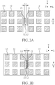
- FIG. 3A is a top view showing the relationship between electronic modules 12 and sensing elements 13 of the present embodiment, which are enlarged views of a part of the electronic device shown in FIG. 1 . More specifically, as shown in FIG. 1, FIG. 2A and FIG. 3A , the sensing element 13 comprises a semiconductor layer 131, and the electronic modules 12 are arranged in a manner to expose the semiconductor layer 131 of the sensing element 13.
- the term "the electronic modules 12 arranged in a manner to expose the semiconductor layer 131 of the sensing element 13" refers to the situation that signals emitted by the electronic modules 12 can be sensed by the semiconductor layer 131 of the sensing elements 13 no matter whether or not the semiconductor layer 131 of the sensing elements 13 are overlapped with the electronic modules 12 in the normal direction Z of the substrate 11.
- the semiconductor layer 131 of the sensing elements 13 can be considered to be exposed from the electronic modules 12 when the signals emitted by the electronic modules 12 can be sensed by the sensing elements 13.
- FIG. 2A and FIG. 3A show that the sensing element 13, especially the semiconductor layer 131 is not overlapped with the electronic modules 12 in the normal direction Z of the substrate 11.
- the gaps between two adjacent electronic modules 12 shown in FIG. 2B and FIG. 3B are narrower than the gap between two adjacent electronic modules 12 shown in FIG. 2A and FIG. 3A , and the sensing element 13, especially the semiconductor layer 131, is partially overlapped with the electronic modules 12 in the normal direction Z of the substrate 11.
- the electronic modules 12 may comprise other elements (for example, a reflective element) capable of introducing the signals emitted by the electronic modules 12 into the sensing element 13, so the sensing element 13, especially the semiconductor layer 131, can detect the signals.
- the sensing elements 13 are not disposed at the gap between two adjacent electronic modules 12 but may be disposed under the electronic modules 12 and near the gap, and the electronic modules 12 may comprise other elements (for example, a reflective element) capable of introducing the signals emitted by the electronic modules 12 into the sensing elements 13, so the sensing elements 13 can detect the signals.
- the sensing elements 13 are disposed under the electronic modules 12 and are completely overlapped with the electronic modules 12 in the normal direction Z of the substrate 11, the sensing elements 13, especially the semiconductor layers 131, still can sense the signals emitted by the electronic modules 12.
- other optical elements such as micro-lenses may be disposed on the sensing elements 13 to facilitate the sensing elements 13 sensing the signals emitted by the electronic modules 12.
- the electronic elements 121 are light emitting diodes, antenna units or a combination thereof.
- the electronic elements 121 are light emitting diodes.
- the light emitting diodes capable of using in the electronic device of the present embodiment can be organic light-emitting diodes (OLED), normal light-emitting diodes (normal LEDs), mini light-emitting diodes (mini-LEDs), micro light-emitting diodes (micro-LEDs), or quantum-dot light-emitting diodes (QLEDs or QD-LEDs).
- the light emitting diode can emit visible light, laser, infrared, or ultraviolet (UV) light, but the present disclosure is not limited thereto.
- the semiconductor layer 131 has a first area Al, the semiconductor layer 131 has a second area A2 being exposed by the electronic modules 12, and a ratio of the second area A2 to the first area A1 is in a range from 1/3 to 1 (1/3 ⁇ A2/A1 ⁇ 1). More specifically, the semiconductor layer 131 has a first area A1, at least a part of the semiconductor layer 131 not overlapped with the electronic modules 12 in a normal direction Z of the substrate 11 (as shown in FIG. 1 ) has a second area A2, and a ratio of the second area A2 to the first area A1 is in a range from 1/3 to 1 (1/3 ⁇ A2/A1 ⁇ 1). In the aspect shown in FIG.
- the semiconductor layer 131 are not overlapped with the electronic modules 12 in a normal direction Z of the substrate 11 (as shown in FIG. 1 ), so the ratio of the second area A2 to the first area A1 is 1.
- a part of the semiconductor layer 131 are overlapped with the electronic modules 12 in the normal direction Z, so the ratio of the second area A2 to the first area A1 is less than 1 but equal to or greater than 1/3.
- the semiconductor layer 131 of the sensing element 13 has a first length L1 in the first direction X and a second length L2 in a second direction Y different from the first direction X, and the first length L1 is less than the second length L2.
- the first direction X is perpendicular to the second direction Y.
- the second length L2 increases, the first area A1 of the semiconductor layer 131 can be increased.
- the sensitivity or accuracy of the sensing element 13 can be enhanced.
- FIG. 4A to FIG. 4D are cross-sectional views of sensing elements according to different aspects of the present disclosure.
- a first insulating layer 112 is disposed on the substrate 11
- a driving semiconductor layer 131' is disposed on the first insulating layer 112
- a gate insulating layer 113 is disposed on the driving semiconductor layer 131'
- a first gate electrode 134' is disposed on the gate insulating layer 113
- a third insulating layer 114 is disposed on the first gate electrode 134'
- a semiconductor layer 131 is disposed on the third insulating layer 114
- a fourth insulating layer 115 is disposed on the semiconductor layer 131
- a first electrode 132, a second electrode 133, a third electrode 132' and a fourth electrode 133' are disposed on the fourth insulating layer 115
- a planer layer 116 is disposed on the first electrode 132, the second electrode 133, the third electrode 132' and the fourth electrode 133
- the driving semiconductor layer 131', the first gate electrode 134', the third electrode 132' and the fourth electrode 133' constitute a transistor TFT which is comprised in the circuit layer 111 (as shown in FIG. 2A ).
- the transistor is a top gate transistor, and the transistor can be a bottom gate transistor in another embodiment of the present disclosure.
- the sensing element 13 is a PIN type sensing element, but the present disclosure is not limited thereto.
- the sensing element 13 comprises: the semiconductor layer 131; the first electrode 132 electrically connected to the semiconductor layer 131; and the second electrode 133 electrically connected to the semiconductor layer 131.
- the semiconductor layer 131 comprises a first semiconductor layer 131a, a second semiconductor layer 131b and a third semiconductor layer 131c sequentially laminated on the substrate 11.
- One of the first semiconductor layer 131a and the third semiconductor layer 131c is a p-doped semiconductor layer, the other one is an n-doped semiconductor layer, and the second semiconductor layer 131b is an intrinsic semiconductor layer (also called as a depletion layer).
- the first electrode 132 is electrically connected to the fourth electrode 133', so the transistor TFT can drive the sensing element 13.
- FIG. 4B The structure shown in FIG. 4B is similar to that shown in FIG. 4A , except for the structure of the sensing element 13.
- a part of the second semiconductor layer 131b and a part of the third semiconductor layer 131c are disposed on the third insulating layer 114.
- the second semiconductor layer 131b is only disposed on the first semiconductor layer 131a
- the third semiconductor layer 131c is only disposed on the second semiconductor layer 131b.
- the first area A1 and the second area A2 indicated in FIG. 3A and FIG. 3B are defined by the area of the overall semiconductor layer 131 including the first semiconductor layer 131a, the second semiconductor layer 131b and the third semiconductor layer 131c shown in FIG. 4A and FIG. 4B .
- a first insulating layer 112 is disposed on the substrate 11, a driving semiconductor layer 131' is disposed on the first insulating layer 112, a gate insulating layer 113 is disposed on the driving semiconductor layer 131', a first gate electrode 134' and a second gate electrode 134 are disposed on the gate insulating layer 113, a third insulating layer 114 is disposed on the first gate electrode 134' and the second gate electrode 134, a semiconductor layer 131 is disposed on the third insulating layer 114, a fourth insulating layer 115 is disposed on the semiconductor layer 131, a first electrode 132, a second electrode 133, a third electrode 132' and a fourth electrode 133' are disposed on the fourth insulating layer 115, and a planer layer 116 is disposed on the first electrode 132, the second electrode 133, the third electrode 132' and the fourth electrode 133'.
- the sensing element 13 is a TFT type sensing element, which comprises: the second gate electrode 134; the semiconductor layer 131 corresponding to the second gate electrode 134; the first electrode 132 electrically connected to the semiconductor layer 131; and the second electrode 133 electrically connected to the semiconductor layer 131.
- the first electrode 132 is electrically connected to the fourth electrode 133', so the transistor TFT can drive the sensing element 13.
- FIG. 4D The structure shown in FIG. 4D is similar to that shown in FIG. 4C , except that the transistor TFT shown in FIG. 4D is a bottom gate transistor.
- the first insulating layer 112, the gate insulating layer 113, the third insulating layer 114, the fourth insulating layer 115 and the planer layer 116 may respectively comprise silicon oxide, silicon oxynitride, silicon nitride, aluminum oxide, resin, polymer, photoresist, or a combination thereof.
- the first gate electrode 134', the second gate electrode 134, the first electrode 132, the second electrode 133, the third electrode 132' and the fourth electrode 133' may respectively comprise Cu, Al, Mo, W, Au, Cr, Ni, Pt, Ti, alloy thereof, other suitable metal, a combination thereof, or other conductive material with good conductivity or small resistance.
- the first semiconductor layer 131a, the second semiconductor layer 131b, the third semiconductor layer 131c, the driving semiconductor layer 131' or the semiconductor layer 131 may comprise amorphous silicon, polycrystalline-silicon, or metal oxide such as IGZO (indium gallium zinc oxide), AIZO (aluminum indium zinc oxide), HIZO (hafnium indium zinc oxide), ITZO (indium tin zinc oxide), IGZTO (indium gallium zinc tin oxide), or IGTO (indium gallium tin oxide).
- IGZO indium gallium zinc oxide
- AIZO aluminum indium zinc oxide
- HIZO hafnium indium zinc oxide
- ITZO indium tin zinc oxide
- IGZTO indium gallium zinc tin oxide
- IGTO indium gallium tin oxide
- the sensing elements 13 shown in FIG. 4A to FIG. 4D can be used alone or in combination in the electronic device of the present disclosure.
- the present disclosure is not limited thereto, and other type of sensing elements or other type of driving elements for driving the sensing element may also be used in the electronic device of the present disclosure.
- the sensing elements 13 can be formed together with the circuit layer 111 shown in FIG. 2A and FIG. 2B , so there is no need to form the sensing elements 13 by another manufacturing process or to additionally dispose the sensing elements 13 on the substrate 11. Thus, the cost for forming the sensing elements 13 can be reduced. But in another embodiment of the present disclosure, at least one of the sensing elements 13 are externally disposed on the substrate 11, and electrically connect to the circuit layer 111 which is shown in FIG. 2A and FIG. 2B . When the sensing element 13 is out of function, the external sensing element 13 can be replaced more easily.
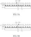
- FIG. 5A and FIG. 5B are cross-sectional views showing first signals emitted by one of the electronic modules and sensed by sensing elements according to one embodiment of the present disclosure, wherein the electronic elements 121 in the enabled state are present with filling patterns, and the electronic elements 121 in the disabled state are present with blank.
- At least two of the electronic modules 12 are sensed by at least one of the sensing elements 13. More specifically, at least two first signals respectively emitted by at least two of the electronic modules 12 are sensed by at least one of the sensing elements 13.
- the first signal may comprise light, heat, electromagnetic wave, radio frequency wave, etc.
- the sensing elements 13 can be photo sensors, thermal sensors, electromagnetic wave sensors, radio frequency wave sensors or a combination thereof.
- the electronic element 121a is in the enabled state and the electronic element 121b is in the disabled state, and the first signal emitted by the electronic element 121a of the electronic modules 12 disposed on the left side of the sensing element 13 can be sensed by the sensing element 13.
- the electronic element 121b is in the enabled state and the electronic element 121a is in the disabled state, and the first signal emitted by the electronic element 121b of the electronic modules 12 disposed on the right side of the sensing element 13 can be sensed by the sensing element 13.
- the signals emitted by the electronic element 121a and the signal emitted by the electronic element 121b may be identical or different.
- the sensing element 13 After the sensing element 13 receive the first signals emitted by the electronic elements 121a or 121b, the sensing element 13 can output at least one second signal according to the first signals. Then, the controller 14 (as shown in FIG. 1 ) can calibrate the electronic modules 12, in which the electronic elements 121a, 121b are comprised therein, according to the at least one second signal.
- the electronic elements 121 are light emitting diodes, antenna units or a combination thereof.
- the electronic elements 121 are light emitting diodes.
- the light emitting diodes capable of using in the electronic device of the present embodiment can be organic light-emitting diodes (OLED), normal light-emitting diodes (normal LEDs), mini light-emitting diodes (mini-LEDs), micro light-emitting diodes (micro-LEDs), or quantum-dot light-emitting diodes (QLEDs or QD-LEDs).
- the light emitting diode can emit visible light, laser, infrared, or ultraviolet (UV) light, but the present disclosure is not limited thereto.
- the electronic device of the present embodiment is a tiled LED display device.
- the tiled LED display device is constituted by electronic modules 12, and the properties (such as electrical impedance, hues of LEDs, etc.) of each electronic module 12 may be different, resulting in that the image displayed on the tiled LED display device is non-uniform.
- the first signals emitted by the electronic elements 121a, 121b of different electronic modules 12 can be sensed by the sensing element 13, so the non-uniformity caused by the difference between the properties of the electronic modules 12 corresponding to the electronic elements 121a, 121b can be detected by the sensing element 13.
- the controller 14 can calibrate the outputs of the electronic modules 12 corresponding to first signals of the electronic elements 121a, 121b to solve the problem of non-uniform image.
- the sensing element 13 by disposing the sensing element 13 in the tiled display device, there is no need to dispose additional IC chips corresponding to each electronic module 12, and the cost of the tiled display device can be reduced.
- the first signals are sequentially emitted by the electronic modules 12 where the electronic elements 121a, 121b are disposed. In other embodiment, the first signals can be simultaneously emitted by the electronic modules 12.
- FIG. 6A and FIG. 6B are top views showing first signals sequentially emitted by electronic modules according to different embodiments of the present disclosure, wherein the electronic elements 121 in the enabled state are present with filling patterns, and the electronic elements 121 in the disabled state are present with blank.
- the electronic elements 121 of one electronic module 12(a) adjacent to the sensing elements 13 are in the enabled state first, and the sensing elements 13 can sense the first signals emitted from the electronic elements 121 of the electronic module 12(a) in the enabled state.
- the electronic elements 121 of another electronic module 12(b) adjacent to the sensing elements 13 are in the enabled state, and the sensing elements 13 can sense the first signals emitted from the electronic elements 121 of the electronic module 12(b) in the enabled state.
- the sensing elements 13 can sense the first signals emitted by these electronic elements 121 of the electronic modules 12(a), 12(b) in the enabled state.
- FIG. 6A and FIG. 6B show the examples that the first signals are sequentially emitted by the electronic elements 121 of the electronic modules 12(a), 12(b) and the sensing elements 13 sense the first signals emitted by the electronic modules 12(a), 12(b) in the enabled state.
- the present disclosure is not limited thereto. The number or the arrangement the electronic elements 121 in the enabled state can be adjusted according to the actual demand.
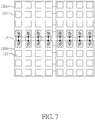
- FIG. 7 is a top view showing first signals simultaneously emitted by electronic modules according to one embodiment of the present disclosure, wherein the electronic elements 121 in the enabled state are present with filling patterns, and the electronic elements 121 in the disabled state are present with blank. As shown in FIG. 7 , all the electronic elements 121 of the electronic modules 12(a), 12(b) adjacent to the sensing elements 13 are simultaneously in the enabled state, and the sensing elements 13 can sense the first signals emitted by the electronic elements 121 of the electronic modules 12(a), 12(b) in the enabled state.
- FIG. 7 is a top view showing first signals simultaneously emitted by electronic modules according to one embodiment of the present disclosure, wherein the electronic elements 121 in the enabled state are present with filling patterns, and the electronic elements 121 in the disabled state are present with blank.
- all the electronic elements 121 of the electronic modules 12(a), 12(b) adjacent to the sensing elements 13 are simultaneously in the enabled state, and the sensing elements 13 can sense the first signals emitted by the electronic elements 121 of
- the present disclosure is not limited thereto.
- the number or the arrangement the electronic elements 121 in the enabled state can be adjusted according to the actual demand.
- FIG. 8A to FIG. 8F are top views of electronic devices according to different embodiments of the present disclosure.
- the electronic modules 12 can be arranged in an array. In other embodiments of the present disclosure, the electronic modules 12 may not be arranged in an array.
- the sensing elements 13 are disposed between at least two adjacent electronic modules 12 so that the sensing elements 13 can sense the signals from the electronic modules 12, the arrangement of the electronic modules 12 is not limited to those shown in FIG. 8A to FIG. 8F and can be adjust according to the actual demand.
- the electronic modules 12 have rectangle shapes. As shown in FIG. 8B , the electronic modules 12 have hexagon shapes. However, the present disclosure is not limited thereto, and the electronic modules 12 may have other shapes.
- the electronic device may further comprise at least one connector 16 connecting two of the electronic modules 12.
- the connector 16 may be a circuit board electrically connecting to the electronic modules 12.
- the connector 16 may be a connecting substrate which physically connect to but does not electrically connect to the electronic modules 12.
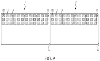
- FIG. 9 is a perspective view of an electronic system according to one embodiment of the present disclosure.
- the electronic system of the present embodiment comprises at least two electronic devices 1, 2, so the electronic system of the present embodiment is a tiled electronic system.
- the electronic device 1, 2 are similar to those shown in FIG. 1 , except that the electronic devices 1, 2 may further comprise additional sensing elements 13 disposed near the edges 1a, 2a of the electronic devices 1, 2.
- the sensing elements 13 disposed near the edge 1a of the electronic device 1 can detect the electronic modules 12 of the electronic devices 1, 2.
- the electronic device made as described in any of the embodiments of the present disclosure is a display device
- the electronic device can be applied to any electronic devices that need a display screen, such as displays, mobile phones, laptops, video cameras, still cameras, music players, mobile navigators, TV sets, public information displays, and other electronic devices that display images.
- the tiled electronic system made as described in any of the embodiments of the present disclosure is a tiled display system
- the tiled electronic system can be applied to any electronic devices that need to display large images, such as video walls, and advertising boards.
Landscapes
- Engineering & Computer Science (AREA)
- Physics & Mathematics (AREA)
- General Physics & Mathematics (AREA)
- Theoretical Computer Science (AREA)
- Computer Hardware Design (AREA)
- Multimedia (AREA)
- Photometry And Measurement Of Optical Pulse Characteristics (AREA)
- Devices For Indicating Variable Information By Combining Individual Elements (AREA)
- Semiconductor Integrated Circuits (AREA)
Abstract
Description
- The present disclosure relates to an electronic device. More specifically, the present disclosure relates to an electronic device comprising tiled electronic modules.
- With the continuous advancement of technologies related to display devices, the applications of the display devices are not limited to monitors, mobile phones, laptops, televisions, etc. Nowadays, tiled display device or tiled display systems are developed to extend the applications of the display devices to video walls, advertising boards, and other electronic devices for displaying large images.
- However, the tiled display device or the tiled display system may suffer from the problem that the properties of the electronic modules comprised therein are different, resulting in that the whole image displayed thereon is non-uniform.
- It is an object of the present invention to provide an electronic device, particularly a tiled display device or tiled display system, which is configured to display more uniform images.
- This problem is solved by an electronic device as claimed by
claim 1 and 11, respectively. Further advantageous embodiments are the subject-matter of the dependent claims. - The present disclosure provides an electronic device, which comprises: a substrate; a plurality of sensing elements disposed on the substrate; and a plurality of electronic modules disposed on the substrate, each electronic module comprising a plurality of electronic elements, wherein the plurality of electronic modules are arranged in a manner to expose the plurality of sensing elements.
- The present disclosure further provides another electronic device, which comprises: a substrate; a plurality of sensing elements disposed on the substrate; and a plurality of electronic modules disposed on the substrate, each electronic module comprising a plurality of electronic elements, wherein at least two of the electronic modules are sensed by at least one of the sensing elements.
- The present disclosure also provides another electronic device, which comprises: a substrate; a plurality of sensing elements disposed on the substrate; and a plurality of electronic modules disposed on the substrate; wherein at least one of the plurality of electronic modules comprises a plurality of electronic elements, and the plurality of electronic modules are arranged in a manner to expose the plurality of sensing elements.
- Other novel features of the disclosure will become more apparent from the following detailed description when taken in conjunction with the accompanying drawings.
-
-
FIG. 1 is a top view of an electronic device according to one embodiment of the present disclosure. -
FIG. 2A and FIG. 2B are cross-sectional views of electronic devices according to different embodiments of the present disclosure. -
FIG. 3A and FIG. 3B are top views showing the relationships between electronic modules and sensing elements according to different aspects of the present disclosure. -
FIG. 4A to FIG. 4D are cross-sectional views of sensing elements according to different aspects of the present disclosure. -
FIG. 5A and FIG. 5B are cross-sectional views showing first signals emitted by one of the electronic modules and sensed by sensing elements according to one embodiment of the present disclosure. -
FIG. 6A andFIG. 6B are top views showing first signals sequentially emitted by electronic modules according to different embodiments of the present disclosure. -
FIG. 7 is a top view showing first signals simultaneously emitted by electronic modules according to one embodiment of the present disclosure. -
FIG. 8A to FIG. 8F are top views of electronic devices according to different embodiments of the present disclosure. -
FIG. 9 is a perspective view of an electronic system according to one embodiment of the present disclosure. - The following embodiments when read with the accompanying drawings are made to clearly exhibit the above-mentioned and other technical contents, features and/or effects of the present disclosure. Through the exposition by means of the specific embodiments, people would further understand the technical means and effects the present disclosure adopts to achieve the above-indicated objectives. Moreover, as the contents disclosed herein should be readily understood and can be implemented by a person skilled in the art, all equivalent changes or modifications which do not depart from the concept of the present disclosure should be encompassed by the appended claims.
- Furthermore, the ordinals recited in the specification and the claims such as "first", "second" and so on are intended only to describe the elements claimed and imply or represent neither that the claimed elements have any proceeding ordinals, nor that sequence between one claimed element and another claimed element or between steps of a manufacturing method. The use of these ordinals is merely to differentiate one claimed element having a certain designation from another claimed element having the same designation.
- Furthermore, the terms recited in the specification and the claims such as "above", "over", or "on" are intended not only directly contact with the other element, but also intended indirectly contact with the other element. Similarly, the terms recited in the specification and the claims such as "below", or "under" are intended not only directly contact with the other element but also intended indirectly contact with the other element.
- Furthermore, the terms recited in the specification and the claims such as "connect" is intended not only directly connect with other element, but also intended indirectly connect and electrically connect with other element.
- Furthermore, when a value is in a range from a first value to a second value, the value can be the first value, the second value, or another value between the first value and the second value.
- Furthermore, the terms "about", "nearly", "almost", "approximately", or "substantially" are usually expressed within 20% of a given value or range, or within 10%, or within 5%, or within 3%, or within 2%, or within 1%, or within 0.5%. The quantity given here is an approximate quantity, that is, in the absence of specific descriptions of "about", "nearly", "almost", "approximately", or "substantially", the meaning of "about", "nearly", "almost", "approximately", or "substantially" may still be implied.
- In addition, the features in different embodiments of the present disclosure can be mixed to form another embodiment.
-
FIG. 1 is a top view of an electronic device according to one embodiment of the present disclosure. The electronic device of the present embodiment comprises: asubstrate 11; a plurality ofsensing elements 13 disposed on thesubstrate 11; and a plurality ofelectronic modules 12 disposed on thesubstrate 11, wherein each of theelectronic modules 12 comprises a plurality ofelectronic elements 121. In some other embodiments, at least oneelectronic module 12 comprises a plurality ofelectronic elements 121. In addition, the electronic device of the present embodiment may further comprise acontroller 14 electrically connected to thesubstrate 11. Herein, thecontroller 14 is electrically connected to thesubstrate 11 via acircuit board 15. In addition, thecontroller 14 can be a timing controller (T-con controller), but the present disclosure is not limited thereto. - In the present embodiment, the
electronic modules 12 are disposed on thesubstrate 11 and arranged in juxtaposition to form a tiled electronic device. InFIG. 1 , not all theelectronic modules 12 but only fourelectronic modules 12 are shown. However, the present disclosure is not limited thereto. The number and the arrangement of theelectronic modules 12 can be adjusted according to the actual demand. In addition, inFIG. 1 , each of theelectronic modules 12 comprises nineelectronic elements 121, but the present disclosure is not limited thereto. The number and the arrangement of theelectronic elements 121 can be adjusted according to the actual demand. -
FIG. 2A is a cross-sectional view of the electronic device of the present embodiment along the line I-I' indicated inFIG. 1 . Thesubstrate 11 used in the electronic device of the present embodiment is a driving substrate with acircuit layer 111 formed thereon, and theelectronic modules 12 are electrically connected to thecircuit layer 111 on thesubstrate 11 throughconductive elements 123. Theelectronic modules 12 used in the electronic device of the present embodiment may respectively comprise: afirst substrate 122; and a plurality ofelectronic elements 121 disposed on thefirst substrate 122. Herein, thesubstrate 11 and thefirst substrate 122 may respectively comprise a printed circuit board (PCB), a quartz substrate, a glass substrate, a wafer, a sapphire substrate, or etc. Alternatively, thesubstrate 11 and thefirst substrate 122 may also respectively comprise a flexible substrate or a film, and the material of which can comprise polycarbonate (PC), polyimide (PI), polypropylene (PP), polyethylene terephthalate (PET), other plastic or polymer materials, or the combination thereof. When the flexible substrate or the film is used, the electronic device can be a flexible electronic device. However, the present disclosure is not limited thereto. - As shown in
FIG. 2A , theelectronic modules 12 are electrically connected to thecircuit layer 111 on thesubstrate 11 throughconductive elements 123. Theconductive elements 123 can respectively be a solder bump, a metal pillar, or a medium including conductive particles. Theconductive elements 123 may respectively comprise Ag, Al, Ni, Cr, Cu, Au, Pd, Pt, Sn, W, Rh, Jr, Ru, Mg, Zn, an alloy thereof, or a combination thereof, but the present disclosure is not limited to. Alternatively, theconductive elements 123 can be formed by using conductive paste such as Ag paste or an anisotropic conductive film (ACF), but the present disclosure is not limited thereto. - As show in
FIG. 1 and FIG. 2A , the electronic device of the present embodiment comprises thesensing elements 13 disposed on thesubstrate 11, and theelectronic modules 12 are arranged in a manner to expose thesensing elements 13. In the present disclosure, the term "theelectronic modules 12 are arranged in a manner to expose thesensing elements 13" refers to the situation that signals emitted by theelectronic modules 12 can be sensed by thesensing elements 13 no matter whether or not thesensing elements 13 are overlapped with theelectronic modules 12 in the normal direction Z of thesubstrate 11. Thus, in the situations that thesensing elements 13 are completely overlapped, are partially overlapped, or are not overlapped with theelectronic modules 12 in the normal direction Z of thesubstrate 11, thesensing elements 13 can be considered to be exposed from theelectronic modules 12 when the signals emitted by theelectronic modules 12 can be sensed by thesensing elements 13. - Further, in the present disclosure, the term "signals emitted by the electronic modules can be sensed by the sensing element" or "the electronic modules are sensed by the sensing element" means the signals sensed by the
sensing element 13 are emitted by one or moreelectronic elements 121 disposed on theelectronic modules 12. More specifically, thesensing element 13 can receive the dedicated signals emitted by one or moreelectronic elements 121, or detect the strength of the outputs (such as light or heat) emitted by one or moreelectronic elements 121. -
FIG. 3A is a top view showing the relationship betweenelectronic modules 12 andsensing elements 13 of the present embodiment, which are enlarged views of a part of the electronic device shown inFIG. 1 . More specifically, as shown inFIG. 1, FIG. 2A andFIG. 3A , thesensing element 13 comprises asemiconductor layer 131, and theelectronic modules 12 are arranged in a manner to expose thesemiconductor layer 131 of thesensing element 13. In the present disclosure, the term "theelectronic modules 12 arranged in a manner to expose thesemiconductor layer 131 of thesensing element 13" refers to the situation that signals emitted by theelectronic modules 12 can be sensed by thesemiconductor layer 131 of thesensing elements 13 no matter whether or not thesemiconductor layer 131 of thesensing elements 13 are overlapped with theelectronic modules 12 in the normal direction Z of thesubstrate 11. Thus, in the situations that thesemiconductor layer 131 of thesensing elements 13 are completely overlapped, are partially overlapped, or are not overlapped with theelectronic modules 12 in the normal direction Z of thesubstrate 11, thesemiconductor layer 131 of thesensing elements 13 can be considered to be exposed from theelectronic modules 12 when the signals emitted by theelectronic modules 12 can be sensed by thesensing elements 13. -
FIG. 2A andFIG. 3A show that thesensing element 13, especially thesemiconductor layer 131 is not overlapped with theelectronic modules 12 in the normal direction Z of thesubstrate 11. In another embodiment of the present disclosure, the gaps between two adjacentelectronic modules 12 shown inFIG. 2B andFIG. 3B are narrower than the gap between two adjacentelectronic modules 12 shown inFIG. 2A andFIG. 3A , and thesensing element 13, especially thesemiconductor layer 131, is partially overlapped with theelectronic modules 12 in the normal direction Z of thesubstrate 11. Herein, theelectronic modules 12 may comprise other elements (for example, a reflective element) capable of introducing the signals emitted by theelectronic modules 12 into thesensing element 13, so thesensing element 13, especially thesemiconductor layer 131, can detect the signals. - In further another embodiment of the present disclosure, even not shown in the figure, the
sensing elements 13 are not disposed at the gap between two adjacentelectronic modules 12 but may be disposed under theelectronic modules 12 and near the gap, and theelectronic modules 12 may comprise other elements (for example, a reflective element) capable of introducing the signals emitted by theelectronic modules 12 into thesensing elements 13, so thesensing elements 13 can detect the signals. Thus, even though thesensing elements 13 are disposed under theelectronic modules 12 and are completely overlapped with theelectronic modules 12 in the normal direction Z of thesubstrate 11, thesensing elements 13, especially the semiconductor layers 131, still can sense the signals emitted by theelectronic modules 12. - In one embodiment of the present embodiment, other optical elements such as micro-lenses may be disposed on the
sensing elements 13 to facilitate thesensing elements 13 sensing the signals emitted by theelectronic modules 12. - In the electronic device of the present embodiment, the
electronic elements 121 are light emitting diodes, antenna units or a combination thereof. In one embodiment of the present disclosure, theelectronic elements 121 are light emitting diodes. Herein, the light emitting diodes capable of using in the electronic device of the present embodiment can be organic light-emitting diodes (OLED), normal light-emitting diodes (normal LEDs), mini light-emitting diodes (mini-LEDs), micro light-emitting diodes (micro-LEDs), or quantum-dot light-emitting diodes (QLEDs or QD-LEDs). In some embodiments of the present disclosure, the light emitting diode can emit visible light, laser, infrared, or ultraviolet (UV) light, but the present disclosure is not limited thereto. - As shown in
FIG. 3A and FIG. 3B , thesemiconductor layer 131 has a first area Al, thesemiconductor layer 131 has a second area A2 being exposed by theelectronic modules 12, and a ratio of the second area A2 to the first area A1 is in a range from 1/3 to 1 (1/3≦A2/A1≦1). More specifically, thesemiconductor layer 131 has a first area A1, at least a part of thesemiconductor layer 131 not overlapped with theelectronic modules 12 in a normal direction Z of the substrate 11 (as shown inFIG. 1 ) has a second area A2, and a ratio of the second area A2 to the first area A1 is in a range from 1/3 to 1 (1/3≤A2/A1≤ 1). In the aspect shown inFIG. 3A , thesemiconductor layer 131 are not overlapped with theelectronic modules 12 in a normal direction Z of the substrate 11 (as shown inFIG. 1 ), so the ratio of the second area A2 to the first area A1 is 1. In the aspect shown inFIG. 3B , a part of thesemiconductor layer 131 are overlapped with theelectronic modules 12 in the normal direction Z, so the ratio of the second area A2 to the first area A1 is less than 1 but equal to or greater than 1/3. - As shown in
FIG. 3A and FIG. 3B , two adjacentelectronic modules 12 are separated from each other in a first direction X to expose thesensing element 13, thesemiconductor layer 131 of thesensing element 13 has a first length L1 in the first direction X and a second length L2 in a second direction Y different from the first direction X, and the first length L1 is less than the second length L2. In some embodiments of the disclosure, the first direction X is perpendicular to the second direction Y. When the second length L2 increases, the first area A1 of thesemiconductor layer 131 can be increased. Thus, the sensitivity or accuracy of thesensing element 13 can be enhanced. -
FIG. 4A to FIG. 4D are cross-sectional views of sensing elements according to different aspects of the present disclosure. As shown inFIG. 4A , a first insulatinglayer 112 is disposed on thesubstrate 11, a driving semiconductor layer 131' is disposed on the first insulatinglayer 112, agate insulating layer 113 is disposed on the driving semiconductor layer 131', a first gate electrode 134' is disposed on thegate insulating layer 113, a thirdinsulating layer 114 is disposed on the first gate electrode 134', asemiconductor layer 131 is disposed on the third insulatinglayer 114, a fourth insulatinglayer 115 is disposed on thesemiconductor layer 131, afirst electrode 132, asecond electrode 133, a third electrode 132' and a fourth electrode 133' are disposed on the fourth insulatinglayer 115, and aplaner layer 116 is disposed on thefirst electrode 132, thesecond electrode 133, the third electrode 132' and the fourth electrode 133'. The driving semiconductor layer 131', the first gate electrode 134', the third electrode 132' and the fourth electrode 133' constitute a transistor TFT which is comprised in the circuit layer 111 (as shown inFIG. 2A ). Herein, the transistor is a top gate transistor, and the transistor can be a bottom gate transistor in another embodiment of the present disclosure. In addition, thesensing element 13 is a PIN type sensing element, but the present disclosure is not limited thereto. Thesensing element 13 comprises: thesemiconductor layer 131; thefirst electrode 132 electrically connected to thesemiconductor layer 131; and thesecond electrode 133 electrically connected to thesemiconductor layer 131. More specifically, thesemiconductor layer 131 comprises afirst semiconductor layer 131a, asecond semiconductor layer 131b and athird semiconductor layer 131c sequentially laminated on thesubstrate 11. One of thefirst semiconductor layer 131a and thethird semiconductor layer 131c is a p-doped semiconductor layer, the other one is an n-doped semiconductor layer, and thesecond semiconductor layer 131b is an intrinsic semiconductor layer (also called as a depletion layer). Thefirst electrode 132 is electrically connected to the fourth electrode 133', so the transistor TFT can drive thesensing element 13. - The structure shown in
FIG. 4B is similar to that shown inFIG. 4A , except for the structure of thesensing element 13. InFIG. 4A , a part of thesecond semiconductor layer 131b and a part of thethird semiconductor layer 131c are disposed on the third insulatinglayer 114. InFIG. 4B , thesecond semiconductor layer 131b is only disposed on thefirst semiconductor layer 131a, and thethird semiconductor layer 131c is only disposed on thesecond semiconductor layer 131b. - In the present disclosure, the first area A1 and the second area A2 indicated in
FIG. 3A and FIG. 3B are defined by the area of theoverall semiconductor layer 131 including thefirst semiconductor layer 131a, thesecond semiconductor layer 131b and thethird semiconductor layer 131c shown inFIG. 4A and FIG. 4B . - As shown in
FIG. 4C , a first insulatinglayer 112 is disposed on thesubstrate 11, a driving semiconductor layer 131' is disposed on the first insulatinglayer 112, agate insulating layer 113 is disposed on the driving semiconductor layer 131', a first gate electrode 134' and asecond gate electrode 134 are disposed on thegate insulating layer 113, a thirdinsulating layer 114 is disposed on the first gate electrode 134' and thesecond gate electrode 134, asemiconductor layer 131 is disposed on the third insulatinglayer 114, a fourth insulatinglayer 115 is disposed on thesemiconductor layer 131, afirst electrode 132, asecond electrode 133, a third electrode 132' and a fourth electrode 133' are disposed on the fourth insulatinglayer 115, and aplaner layer 116 is disposed on thefirst electrode 132, thesecond electrode 133, the third electrode 132' and the fourth electrode 133'. Thesensing element 13 is a TFT type sensing element, which comprises: thesecond gate electrode 134; thesemiconductor layer 131 corresponding to thesecond gate electrode 134; thefirst electrode 132 electrically connected to thesemiconductor layer 131; and thesecond electrode 133 electrically connected to thesemiconductor layer 131. Similarly, thefirst electrode 132 is electrically connected to the fourth electrode 133', so the transistor TFT can drive thesensing element 13. - The structure shown in
FIG. 4D is similar to that shown inFIG. 4C , except that the transistor TFT shown inFIG. 4D is a bottom gate transistor. - As shown in
FIG. 4A to FIG. 4D , the first insulatinglayer 112, thegate insulating layer 113, the third insulatinglayer 114, the fourth insulatinglayer 115 and theplaner layer 116 may respectively comprise silicon oxide, silicon oxynitride, silicon nitride, aluminum oxide, resin, polymer, photoresist, or a combination thereof. The first gate electrode 134', thesecond gate electrode 134, thefirst electrode 132, thesecond electrode 133, the third electrode 132' and the fourth electrode 133' may respectively comprise Cu, Al, Mo, W, Au, Cr, Ni, Pt, Ti, alloy thereof, other suitable metal, a combination thereof, or other conductive material with good conductivity or small resistance. Thefirst semiconductor layer 131a, thesecond semiconductor layer 131b, thethird semiconductor layer 131c, the driving semiconductor layer 131' or thesemiconductor layer 131 may comprise amorphous silicon, polycrystalline-silicon, or metal oxide such as IGZO (indium gallium zinc oxide), AIZO (aluminum indium zinc oxide), HIZO (hafnium indium zinc oxide), ITZO (indium tin zinc oxide), IGZTO (indium gallium zinc tin oxide), or IGTO (indium gallium tin oxide). - The
sensing elements 13 shown inFIG. 4A to FIG. 4D can be used alone or in combination in the electronic device of the present disclosure. However, the present disclosure is not limited thereto, and other type of sensing elements or other type of driving elements for driving the sensing element may also be used in the electronic device of the present disclosure. - Herein, the
sensing elements 13 can be formed together with thecircuit layer 111 shown inFIG. 2A and FIG. 2B , so there is no need to form thesensing elements 13 by another manufacturing process or to additionally dispose thesensing elements 13 on thesubstrate 11. Thus, the cost for forming thesensing elements 13 can be reduced. But in another embodiment of the present disclosure, at least one of thesensing elements 13 are externally disposed on thesubstrate 11, and electrically connect to thecircuit layer 111 which is shown inFIG. 2A and FIG. 2B . When thesensing element 13 is out of function, theexternal sensing element 13 can be replaced more easily. - Hereinafter, the functions of the
sensing elements 13 are described in detail.FIG. 5A and FIG. 5B are cross-sectional views showing first signals emitted by one of the electronic modules and sensed by sensing elements according to one embodiment of the present disclosure, wherein theelectronic elements 121 in the enabled state are present with filling patterns, and theelectronic elements 121 in the disabled state are present with blank. - As shown in
FIG. 5A and FIG. 5B , at least two of theelectronic modules 12 are sensed by at least one of thesensing elements 13. More specifically, at least two first signals respectively emitted by at least two of theelectronic modules 12 are sensed by at least one of thesensing elements 13. In the present disclosure, examples of the first signal may comprise light, heat, electromagnetic wave, radio frequency wave, etc. Thus, thesensing elements 13 can be photo sensors, thermal sensors, electromagnetic wave sensors, radio frequency wave sensors or a combination thereof. - In the present embodiment, as shown in
FIG. 5A , theelectronic element 121a is in the enabled state and theelectronic element 121b is in the disabled state, and the first signal emitted by theelectronic element 121a of theelectronic modules 12 disposed on the left side of thesensing element 13 can be sensed by thesensing element 13. Then, as shown inFIG. 5B , theelectronic element 121b is in the enabled state and theelectronic element 121a is in the disabled state, and the first signal emitted by theelectronic element 121b of theelectronic modules 12 disposed on the right side of thesensing element 13 can be sensed by thesensing element 13. It should be noted that the signals emitted by theelectronic element 121a and the signal emitted by theelectronic element 121b may be identical or different. - After the
sensing element 13 receive the first signals emitted by theelectronic elements sensing element 13 can output at least one second signal according to the first signals. Then, the controller 14 (as shown inFIG. 1 ) can calibrate theelectronic modules 12, in which theelectronic elements - In the electronic device of the present embodiment, the
electronic elements 121 are light emitting diodes, antenna units or a combination thereof. In one embodiment of the present disclosure, theelectronic elements 121 are light emitting diodes. Herein, the light emitting diodes capable of using in the electronic device of the present embodiment can be organic light-emitting diodes (OLED), normal light-emitting diodes (normal LEDs), mini light-emitting diodes (mini-LEDs), micro light-emitting diodes (micro-LEDs), or quantum-dot light-emitting diodes (QLEDs or QD-LEDs). In some embodiments of the present disclosure, the light emitting diode can emit visible light, laser, infrared, or ultraviolet (UV) light, but the present disclosure is not limited thereto. - When the
electronic elements 121 are light emitting diodes, the electronic device of the present embodiment is a tiled LED display device. The tiled LED display device is constituted byelectronic modules 12, and the properties (such as electrical impedance, hues of LEDs, etc.) of eachelectronic module 12 may be different, resulting in that the image displayed on the tiled LED display device is non-uniform. In the present embodiment, as shown inFIG. 5A and FIG. 5B , the first signals emitted by theelectronic elements electronic modules 12 can be sensed by thesensing element 13, so the non-uniformity caused by the difference between the properties of theelectronic modules 12 corresponding to theelectronic elements sensing element 13. When thesensing element 13 receives the first signals from theelectronic elements FIG. 1 ), thecontroller 14 can calibrate the outputs of theelectronic modules 12 corresponding to first signals of theelectronic elements sensing element 13 in the tiled display device, there is no need to dispose additional IC chips corresponding to eachelectronic module 12, and the cost of the tiled display device can be reduced. - As shown in
FIG. 5A and FIG. 5B , the first signals are sequentially emitted by theelectronic modules 12 where theelectronic elements electronic modules 12. -
FIG. 6A andFIG. 6B are top views showing first signals sequentially emitted by electronic modules according to different embodiments of the present disclosure, wherein theelectronic elements 121 in the enabled state are present with filling patterns, and theelectronic elements 121 in the disabled state are present with blank. As shown inFIG. 6A , theelectronic elements 121 of one electronic module 12(a) adjacent to thesensing elements 13 are in the enabled state first, and thesensing elements 13 can sense the first signals emitted from theelectronic elements 121 of the electronic module 12(a) in the enabled state. Next, theelectronic elements 121 of another electronic module 12(b) adjacent to thesensing elements 13 are in the enabled state, and thesensing elements 13 can sense the first signals emitted from theelectronic elements 121 of the electronic module 12(b) in the enabled state. In another embodiment of the present disclosure, as shown inFIG. 6B , a portion of theelectronic elements 121 of the electronic modules 12(a), 12(b) adjacent to thesensing elements 13 are in the enabled state first, and thesensing elements 13 can sense the first signals emitted by theseelectronic elements 121 of the electronic modules 12(a), 12(b) in the enabled state. Next, another portion of theelectronic elements 121 of the electronic modules 12(a), 12(b) adjacent to thesensing elements 13 are in the enabled state, and thesensing elements 13 can sense the first signals emitted by the electronic modules 12(a), 12(b) in the enabled state.FIG. 6A andFIG. 6B show the examples that the first signals are sequentially emitted by theelectronic elements 121 of the electronic modules 12(a), 12(b) and thesensing elements 13 sense the first signals emitted by the electronic modules 12(a), 12(b) in the enabled state. However, the present disclosure is not limited thereto. The number or the arrangement theelectronic elements 121 in the enabled state can be adjusted according to the actual demand. -
FIG. 7 is a top view showing first signals simultaneously emitted by electronic modules according to one embodiment of the present disclosure, wherein theelectronic elements 121 in the enabled state are present with filling patterns, and theelectronic elements 121 in the disabled state are present with blank. As shown inFIG. 7 , all theelectronic elements 121 of the electronic modules 12(a), 12(b) adjacent to thesensing elements 13 are simultaneously in the enabled state, and thesensing elements 13 can sense the first signals emitted by theelectronic elements 121 of the electronic modules 12(a), 12(b) in the enabled state.FIG. 7 shows the example that the first signals are simultaneously emitted by theelectronic elements electronic modules 12 and thesensing elements 13 sense the first signals emitted by theelectronic elements 121 of the electronic modules 12(a), 12(b) in the enabled state. However, the present disclosure is not limited thereto. The number or the arrangement theelectronic elements 121 in the enabled state can be adjusted according to the actual demand. -
FIG. 8A to FIG. 8F are top views of electronic devices according to different embodiments of the present disclosure. In some embodiments of the present disclosure, theelectronic modules 12 can be arranged in an array. In other embodiments of the present disclosure, theelectronic modules 12 may not be arranged in an array. However, as long as thesensing elements 13 are disposed between at least two adjacentelectronic modules 12 so that thesensing elements 13 can sense the signals from theelectronic modules 12, the arrangement of theelectronic modules 12 is not limited to those shown inFIG. 8A to FIG. 8F and can be adjust according to the actual demand. - In addition, as shown in
FIG. 8A, and FIG. 8C toFIG. 8F , theelectronic modules 12 have rectangle shapes. As shown inFIG. 8B , theelectronic modules 12 have hexagon shapes. However, the present disclosure is not limited thereto, and theelectronic modules 12 may have other shapes. - Furthermore, as shown in
FIG. 8E and FIG. 8F , the electronic device may further comprise at least oneconnector 16 connecting two of theelectronic modules 12. In one embodiment of the present disclosure, theconnector 16 may be a circuit board electrically connecting to theelectronic modules 12. In another embodiment of the present disclosure, theconnector 16 may be a connecting substrate which physically connect to but does not electrically connect to theelectronic modules 12. -
FIG. 9 is a perspective view of an electronic system according to one embodiment of the present disclosure. The electronic system of the present embodiment comprises at least twoelectronic devices 1, 2, so the electronic system of the present embodiment is a tiled electronic system. Theelectronic device 1, 2 are similar to those shown inFIG. 1 , except that theelectronic devices 1, 2 may further compriseadditional sensing elements 13 disposed near theedges 1a, 2a of theelectronic devices 1, 2. Thus, thesensing elements 13 disposed near the edge 1a of the electronic device 1 can detect theelectronic modules 12 of theelectronic devices 1, 2. - When the electronic device made as described in any of the embodiments of the present disclosure is a display device, the electronic device can be applied to any electronic devices that need a display screen, such as displays, mobile phones, laptops, video cameras, still cameras, music players, mobile navigators, TV sets, public information displays, and other electronic devices that display images. When the tiled electronic system made as described in any of the embodiments of the present disclosure is a tiled display system, the tiled electronic system can be applied to any electronic devices that need to display large images, such as video walls, and advertising boards.
- Although the present disclosure has been explained in relationship to its embodiment, it is to be understood that many other possible modifications and variations can be made without departing from the spirit and scope of the disclosure as hereinafter claimed.
Claims (15)
- An electronic device, comprising:a substrate (11);a plurality of sensing elements (13) disposed on the substrate (11); anda plurality of electronic modules (12) disposed on the substrate (11), each electronic module (12) comprising a plurality of electronic elements (121),wherein the plurality of electronic modules (12) are arranged in a manner to expose the plurality of sensing elements (13).
- The electronic device of claim 1, wherein at least two of the electronic modules (12) are sensed by at least one of the sensing elements (13).
- The electronic device of claim 1 or 2, wherein at least two signals respectively emitted by at least two of the electronic modules (12) are sensed by at least one of the sensing elements (13).
- The electronic device of claim 1, 2 or 3, further comprising a controller (14), wherein the at least one of the sensing elements (13) outputs at least one second signal according to the first signals, and the controller (14) calibrates the electronic modules (12) according to the at least one second signals.
- The electronic device of any one of claims 1 to 4, wherein each sensing element (13) comprises a semiconductor layer (131), and the plurality of electronic modules (12) are arranged in a manner to expose the semiconductor layers (131) of the plurality of sensing elements (13).
- The electronic device of claim 5, wherein one of the semiconductor layers (131) has a first area (A1), the one of the semiconductor layers (131) has a second area (A2) being exposed by the plurality of sensing elements (13), and a ratio of the second area (A2) to the first area (A1) is in a range from 1/3 to 1.
- The electronic device of any one of claims 1 to 4, wherein two of the plurality of electronic modules (12) are separated from each other in a first direction (X) to expose one of the plurality of sensing elements (13), the sensing element (13) comprises a semiconductor layer (131) having a first length (L1) in the first direction (X) and a second length (L2) in a second direction (Y) perpendicular to the first direction (X), and the first length (L1) is less than the second length (L2).
- The electronic device of any one of claims 1 to 7, wherein one of the plurality of sensing elements (13) is a photo sensor, a thermal sensor or a RF wave sensor.
- The electronic device of any one of claims 1 to 8, wherein the plurality of electronic modules (12) are arranged in juxtaposition.
- The electronic device of any one of claims 1 to 8, further comprising at least one connector (16) connecting two of the electronic modules (12).
- An electronic device, comprising:a substrate (11);a plurality of sensing elements (13) disposed on the substrate (11); anda plurality of electronic modules (12) disposed on the substrate (11), each electronic module (12) comprising a plurality of electronic elements (121),wherein at least two of the electronic modules (12) are sensed by at least one of the sensing elements (13).
- The electronic device of claim 11, wherein at least two first signals respectively emitted by the electronic modules (12) are received by the sensing element (13).
- The electronic device of claim 11 or 12, wherein the sensing element (13) outputs at least one second signal according to the first signals.
- The electronic device of claim 13, further comprising a controller (14) calibrating the electronic modules (12) according to the at least one second signal.
- The electronic device of any one of claims 1 to 14, wherein the at least two of the electronic modules (12) emit the first signals sequentially or simultaneously, and the first signals are received by the sensing element (13) sequentially or simultaneously.
Applications Claiming Priority (1)
| Application Number | Priority Date | Filing Date | Title |
|---|---|---|---|
| US16/234,093 US10985148B2 (en) | 2018-12-27 | 2018-12-27 | Electronic device |
Publications (2)
| Publication Number | Publication Date |
|---|---|
| EP3675097A1 true EP3675097A1 (en) | 2020-07-01 |
| EP3675097B1 EP3675097B1 (en) | 2023-09-27 |
Family
ID=68771464
Family Applications (1)
| Application Number | Title | Priority Date | Filing Date |
|---|---|---|---|
| EP19213475.7A Active EP3675097B1 (en) | 2018-12-27 | 2019-12-04 | Electronic device |
Country Status (4)
| Country | Link |
|---|---|
| US (1) | US10985148B2 (en) |
| EP (1) | EP3675097B1 (en) |
| KR (1) | KR102908624B1 (en) |
| CN (1) | CN111384042A (en) |
Families Citing this family (5)
| Publication number | Priority date | Publication date | Assignee | Title |
|---|---|---|---|---|
| EP3588478B1 (en) * | 2018-06-29 | 2022-03-23 | GIO Optoelectronics Corp. | Electronic device |
| EP3608964B1 (en) * | 2018-08-08 | 2022-05-11 | LG Display Co., Ltd. | Stretchable display device |
| KR102664207B1 (en) | 2018-10-08 | 2024-05-07 | 엘지디스플레이 주식회사 | Stretchable display device and manufacturing method the same |
| TWI722405B (en) * | 2019-03-28 | 2021-03-21 | 佳世達科技股份有限公司 | Display pannel |
| CN114138061B (en) * | 2020-09-03 | 2024-11-01 | 财团法人工业技术研究院 | Electronic device |
Citations (3)
| Publication number | Priority date | Publication date | Assignee | Title |
|---|---|---|---|---|
| US20150022754A1 (en) * | 2013-07-19 | 2015-01-22 | Google Inc. | Configurations for tileable display apparatus with multiple pixel arrays |
| WO2017096938A1 (en) * | 2015-12-11 | 2017-06-15 | Boe Technology Group Co., Ltd. | Display device and method for using the same |
| CN108649059A (en) * | 2018-05-14 | 2018-10-12 | 京东方科技集团股份有限公司 | A kind of array substrate, display device and its driving method |
Family Cites Families (15)
| Publication number | Priority date | Publication date | Assignee | Title |
|---|---|---|---|---|
| US6611241B1 (en) * | 1997-12-02 | 2003-08-26 | Sarnoff Corporation | Modular display system |
| US7926300B2 (en) * | 2005-11-18 | 2011-04-19 | Cree, Inc. | Adaptive adjustment of light output of solid state lighting panels |
| KR20090082233A (en) * | 2006-10-20 | 2009-07-29 | 코닌클리즈케 필립스 일렉트로닉스 엔.브이. | Organic light emitting diode device |
| TR200705747A2 (en) * | 2007-08-17 | 2009-03-23 | Vestel Elektroni̇k San. Ve Ti̇c. A.Ş. | Automatic adjustment of backlight and pixel brightness on display panels |
| US8896505B2 (en) * | 2009-06-12 | 2014-11-25 | Global Oled Technology Llc | Display with pixel arrangement |
| KR101333783B1 (en) * | 2009-11-10 | 2013-11-29 | 삼성디스플레이 주식회사 | Organic light emitting diode display and method for manufacturing the same |
| US9064451B2 (en) | 2012-02-01 | 2015-06-23 | Apple Inc. | Organic light emitting diode display having photodiodes |
| US9591726B2 (en) * | 2013-07-02 | 2017-03-07 | Xicato, Inc. | LED-based lighting control network communication |
| US9059337B1 (en) * | 2013-12-24 | 2015-06-16 | Christie Digital Systems Usa, Inc. | Method, system and apparatus for dynamically monitoring and calibrating display tiles |
| US9277618B2 (en) * | 2014-06-27 | 2016-03-01 | Bridgelux, Inc. | Monolithic LED chip in an integrated control module with active circuitry |
| CA2989812C (en) * | 2015-06-26 | 2023-09-26 | Kenall Manufacturing Company | Method of providing doses of light sufficient to deactivate dangerous pathogens throughout a volumetric space over a period of time |
| US11282449B2 (en) | 2016-09-22 | 2022-03-22 | Apple Inc. | Display panel adjustment from temperature prediction |
| KR102581190B1 (en) | 2016-12-14 | 2023-09-21 | 삼성전자주식회사 | Display apparatus and seam correction method thereof |
| CN107146572A (en) | 2017-07-13 | 2017-09-08 | 深圳市洲明科技股份有限公司 | Display screen bearing calibration and its system, computer-readable recording medium |
| KR102604362B1 (en) * | 2018-09-28 | 2023-11-21 | 엘지디스플레이 주식회사 | Sensor package module and organic light emitting display having the same |
-
2018
- 2018-12-27 US US16/234,093 patent/US10985148B2/en active Active
-
2019
- 2019-11-27 KR KR1020190153870A patent/KR102908624B1/en active Active
- 2019-12-02 CN CN201911217077.3A patent/CN111384042A/en active Pending
- 2019-12-04 EP EP19213475.7A patent/EP3675097B1/en active Active
Patent Citations (3)
| Publication number | Priority date | Publication date | Assignee | Title |
|---|---|---|---|---|
| US20150022754A1 (en) * | 2013-07-19 | 2015-01-22 | Google Inc. | Configurations for tileable display apparatus with multiple pixel arrays |
| WO2017096938A1 (en) * | 2015-12-11 | 2017-06-15 | Boe Technology Group Co., Ltd. | Display device and method for using the same |
| CN108649059A (en) * | 2018-05-14 | 2018-10-12 | 京东方科技集团股份有限公司 | A kind of array substrate, display device and its driving method |
Also Published As
| Publication number | Publication date |
|---|---|
| CN111384042A (en) | 2020-07-07 |
| EP3675097B1 (en) | 2023-09-27 |
| KR102908624B1 (en) | 2026-01-06 |
| US20200212021A1 (en) | 2020-07-02 |
| KR20200083212A (en) | 2020-07-08 |
| US10985148B2 (en) | 2021-04-20 |
Similar Documents
| Publication | Publication Date | Title |
|---|---|---|
| EP3675097B1 (en) | Electronic device | |
| US10993347B2 (en) | Electronic device and tiled electronic system comprising the same | |
| US20210391313A1 (en) | Electronic device | |
| US11163392B2 (en) | Display device | |
| US20140048828A1 (en) | Led display panel and led display apparatus | |
| EP3961718B1 (en) | Display device | |
| US12038656B2 (en) | Display device | |
| US9313889B2 (en) | Display apparatus | |
| CN118173573A (en) | Display device | |
| US11852930B2 (en) | Display device | |
| KR100686345B1 (en) | Flat panel display device and manufacturing method | |
| CN100507655C (en) | Liquid crystal display and manufacturing method thereof | |
| US20210359049A1 (en) | Display device | |
| US11522037B2 (en) | Display panel including pads on side surface thereof adjacent connection lines having reduced widths | |
| US20090073098A1 (en) | Display module with identification circuit on panel | |
| US20260033109A1 (en) | Display device | |
| CN113421908B (en) | Display panel and manufacturing method thereof, and display device | |
| US20250133923A1 (en) | Organic light emitting displaying apparatus | |
| US20260033057A1 (en) | Display Apparatus | |
| US20260026165A1 (en) | Display device | |
| US20260082750A1 (en) | Display apparatus | |
| US20260029876A1 (en) | Display Device | |
| US20260026153A1 (en) | Display Device | |
| CN118575290A (en) | Display device | |
| GB2700939A (en) | Display device |
Legal Events
| Date | Code | Title | Description |
|---|---|---|---|
| PUAI | Public reference made under article 153(3) epc to a published international application that has entered the european phase |
Free format text: ORIGINAL CODE: 0009012 |
|
| STAA | Information on the status of an ep patent application or granted ep patent |
Free format text: STATUS: THE APPLICATION HAS BEEN PUBLISHED |
|
| AK | Designated contracting states |
Kind code of ref document: A1 Designated state(s): AL AT BE BG CH CY CZ DE DK EE ES FI FR GB GR HR HU IE IS IT LI LT LU LV MC MK MT NL NO PL PT RO RS SE SI SK SM TR |
|
| AX | Request for extension of the european patent |
Extension state: BA ME |
|
| STAA | Information on the status of an ep patent application or granted ep patent |
Free format text: STATUS: REQUEST FOR EXAMINATION WAS MADE |
|
| 17P | Request for examination filed |
Effective date: 20201230 |
|
| RBV | Designated contracting states (corrected) |
Designated state(s): AL AT BE BG CH CY CZ DE DK EE ES FI FR GB GR HR HU IE IS IT LI LT LU LV MC MK MT NL NO PL PT RO RS SE SI SK SM TR |
|
| STAA | Information on the status of an ep patent application or granted ep patent |
Free format text: STATUS: EXAMINATION IS IN PROGRESS |
|
| 17Q | First examination report despatched |
Effective date: 20220314 |
|
| RIC1 | Information provided on ipc code assigned before grant |
Ipc: G09G 3/20 20060101AFI20230314BHEP |
|
| GRAP | Despatch of communication of intention to grant a patent |
Free format text: ORIGINAL CODE: EPIDOSNIGR1 |
|
| STAA | Information on the status of an ep patent application or granted ep patent |
Free format text: STATUS: GRANT OF PATENT IS INTENDED |
|
| INTG | Intention to grant announced |
Effective date: 20230428 |
|
| GRAS | Grant fee paid |
Free format text: ORIGINAL CODE: EPIDOSNIGR3 |
|
| GRAA | (expected) grant |
Free format text: ORIGINAL CODE: 0009210 |
|
| STAA | Information on the status of an ep patent application or granted ep patent |
Free format text: STATUS: THE PATENT HAS BEEN GRANTED |
|
| AK | Designated contracting states |
Kind code of ref document: B1 Designated state(s): AL AT BE BG CH CY CZ DE DK EE ES FI FR GB GR HR HU IE IS IT LI LT LU LV MC MK MT NL NO PL PT RO RS SE SI SK SM TR |
|
| REG | Reference to a national code |
Ref country code: GB Ref legal event code: FG4D |
|
| REG | Reference to a national code |
Ref country code: CH Ref legal event code: EP |
|
| REG | Reference to a national code |
Ref country code: DE Ref legal event code: R096 Ref document number: 602019038121 Country of ref document: DE |
|
| REG | Reference to a national code |
Ref country code: IE Ref legal event code: FG4D |
|
| REG | Reference to a national code |
Ref country code: LT Ref legal event code: MG9D |
|
| PG25 | Lapsed in a contracting state [announced via postgrant information from national office to epo] |
Ref country code: GR Free format text: LAPSE BECAUSE OF FAILURE TO SUBMIT A TRANSLATION OF THE DESCRIPTION OR TO PAY THE FEE WITHIN THE PRESCRIBED TIME-LIMIT Effective date: 20231228 |
|
| PG25 | Lapsed in a contracting state [announced via postgrant information from national office to epo] |
Ref country code: SE Free format text: LAPSE BECAUSE OF FAILURE TO SUBMIT A TRANSLATION OF THE DESCRIPTION OR TO PAY THE FEE WITHIN THE PRESCRIBED TIME-LIMIT Effective date: 20230927 Ref country code: RS Free format text: LAPSE BECAUSE OF FAILURE TO SUBMIT A TRANSLATION OF THE DESCRIPTION OR TO PAY THE FEE WITHIN THE PRESCRIBED TIME-LIMIT Effective date: 20230927 Ref country code: NO Free format text: LAPSE BECAUSE OF FAILURE TO SUBMIT A TRANSLATION OF THE DESCRIPTION OR TO PAY THE FEE WITHIN THE PRESCRIBED TIME-LIMIT Effective date: 20231227 Ref country code: LV Free format text: LAPSE BECAUSE OF FAILURE TO SUBMIT A TRANSLATION OF THE DESCRIPTION OR TO PAY THE FEE WITHIN THE PRESCRIBED TIME-LIMIT Effective date: 20230927 Ref country code: LT Free format text: LAPSE BECAUSE OF FAILURE TO SUBMIT A TRANSLATION OF THE DESCRIPTION OR TO PAY THE FEE WITHIN THE PRESCRIBED TIME-LIMIT Effective date: 20230927 Ref country code: HR Free format text: LAPSE BECAUSE OF FAILURE TO SUBMIT A TRANSLATION OF THE DESCRIPTION OR TO PAY THE FEE WITHIN THE PRESCRIBED TIME-LIMIT Effective date: 20230927 Ref country code: GR Free format text: LAPSE BECAUSE OF FAILURE TO SUBMIT A TRANSLATION OF THE DESCRIPTION OR TO PAY THE FEE WITHIN THE PRESCRIBED TIME-LIMIT Effective date: 20231228 Ref country code: FI Free format text: LAPSE BECAUSE OF FAILURE TO SUBMIT A TRANSLATION OF THE DESCRIPTION OR TO PAY THE FEE WITHIN THE PRESCRIBED TIME-LIMIT Effective date: 20230927 |
|
| REG | Reference to a national code |
Ref country code: NL Ref legal event code: MP Effective date: 20230927 |
|
| REG | Reference to a national code |
Ref country code: AT Ref legal event code: MK05 Ref document number: 1616219 Country of ref document: AT Kind code of ref document: T Effective date: 20230927 |
|
| PG25 | Lapsed in a contracting state [announced via postgrant information from national office to epo] |
Ref country code: NL Free format text: LAPSE BECAUSE OF FAILURE TO SUBMIT A TRANSLATION OF THE DESCRIPTION OR TO PAY THE FEE WITHIN THE PRESCRIBED TIME-LIMIT Effective date: 20230927 |
|
| PG25 | Lapsed in a contracting state [announced via postgrant information from national office to epo] |
Ref country code: IS Free format text: LAPSE BECAUSE OF FAILURE TO SUBMIT A TRANSLATION OF THE DESCRIPTION OR TO PAY THE FEE WITHIN THE PRESCRIBED TIME-LIMIT Effective date: 20240127 |
|
| PG25 | Lapsed in a contracting state [announced via postgrant information from national office to epo] |
Ref country code: AT Free format text: LAPSE BECAUSE OF FAILURE TO SUBMIT A TRANSLATION OF THE DESCRIPTION OR TO PAY THE FEE WITHIN THE PRESCRIBED TIME-LIMIT Effective date: 20230927 |
|
| PG25 | Lapsed in a contracting state [announced via postgrant information from national office to epo] |
Ref country code: ES Free format text: LAPSE BECAUSE OF FAILURE TO SUBMIT A TRANSLATION OF THE DESCRIPTION OR TO PAY THE FEE WITHIN THE PRESCRIBED TIME-LIMIT Effective date: 20230927 |
|
| PG25 | Lapsed in a contracting state [announced via postgrant information from national office to epo] |
Ref country code: SM Free format text: LAPSE BECAUSE OF FAILURE TO SUBMIT A TRANSLATION OF THE DESCRIPTION OR TO PAY THE FEE WITHIN THE PRESCRIBED TIME-LIMIT Effective date: 20230927 Ref country code: RO Free format text: LAPSE BECAUSE OF FAILURE TO SUBMIT A TRANSLATION OF THE DESCRIPTION OR TO PAY THE FEE WITHIN THE PRESCRIBED TIME-LIMIT Effective date: 20230927 Ref country code: IS Free format text: LAPSE BECAUSE OF FAILURE TO SUBMIT A TRANSLATION OF THE DESCRIPTION OR TO PAY THE FEE WITHIN THE PRESCRIBED TIME-LIMIT Effective date: 20240127 Ref country code: ES Free format text: LAPSE BECAUSE OF FAILURE TO SUBMIT A TRANSLATION OF THE DESCRIPTION OR TO PAY THE FEE WITHIN THE PRESCRIBED TIME-LIMIT Effective date: 20230927 Ref country code: EE Free format text: LAPSE BECAUSE OF FAILURE TO SUBMIT A TRANSLATION OF THE DESCRIPTION OR TO PAY THE FEE WITHIN THE PRESCRIBED TIME-LIMIT Effective date: 20230927 Ref country code: CZ Free format text: LAPSE BECAUSE OF FAILURE TO SUBMIT A TRANSLATION OF THE DESCRIPTION OR TO PAY THE FEE WITHIN THE PRESCRIBED TIME-LIMIT Effective date: 20230927 Ref country code: AT Free format text: LAPSE BECAUSE OF FAILURE TO SUBMIT A TRANSLATION OF THE DESCRIPTION OR TO PAY THE FEE WITHIN THE PRESCRIBED TIME-LIMIT Effective date: 20230927 Ref country code: PT Free format text: LAPSE BECAUSE OF FAILURE TO SUBMIT A TRANSLATION OF THE DESCRIPTION OR TO PAY THE FEE WITHIN THE PRESCRIBED TIME-LIMIT Effective date: 20240129 Ref country code: SK Free format text: LAPSE BECAUSE OF FAILURE TO SUBMIT A TRANSLATION OF THE DESCRIPTION OR TO PAY THE FEE WITHIN THE PRESCRIBED TIME-LIMIT Effective date: 20230927 |
|
| PG25 | Lapsed in a contracting state [announced via postgrant information from national office to epo] |
Ref country code: PL Free format text: LAPSE BECAUSE OF FAILURE TO SUBMIT A TRANSLATION OF THE DESCRIPTION OR TO PAY THE FEE WITHIN THE PRESCRIBED TIME-LIMIT Effective date: 20230927 Ref country code: IT Free format text: LAPSE BECAUSE OF FAILURE TO SUBMIT A TRANSLATION OF THE DESCRIPTION OR TO PAY THE FEE WITHIN THE PRESCRIBED TIME-LIMIT Effective date: 20230927 |
|
| REG | Reference to a national code |
Ref country code: DE Ref legal event code: R097 Ref document number: 602019038121 Country of ref document: DE |
|
| PG25 | Lapsed in a contracting state [announced via postgrant information from national office to epo] |
Ref country code: DK Free format text: LAPSE BECAUSE OF FAILURE TO SUBMIT A TRANSLATION OF THE DESCRIPTION OR TO PAY THE FEE WITHIN THE PRESCRIBED TIME-LIMIT Effective date: 20230927 |
|
| PG25 | Lapsed in a contracting state [announced via postgrant information from national office to epo] |
Ref country code: DK Free format text: LAPSE BECAUSE OF FAILURE TO SUBMIT A TRANSLATION OF THE DESCRIPTION OR TO PAY THE FEE WITHIN THE PRESCRIBED TIME-LIMIT Effective date: 20230927 |
|
| REG | Reference to a national code |
Ref country code: CH Ref legal event code: PL |
|
| PLBE | No opposition filed within time limit |
Free format text: ORIGINAL CODE: 0009261 |
|
| STAA | Information on the status of an ep patent application or granted ep patent |
Free format text: STATUS: NO OPPOSITION FILED WITHIN TIME LIMIT |
|
| PG25 | Lapsed in a contracting state [announced via postgrant information from national office to epo] |
Ref country code: LU Free format text: LAPSE BECAUSE OF NON-PAYMENT OF DUE FEES Effective date: 20231204 |
|
| PG25 | Lapsed in a contracting state [announced via postgrant information from national office to epo] |
Ref country code: MC Free format text: LAPSE BECAUSE OF FAILURE TO SUBMIT A TRANSLATION OF THE DESCRIPTION OR TO PAY THE FEE WITHIN THE PRESCRIBED TIME-LIMIT Effective date: 20230927 |
|
| REG | Reference to a national code |
Ref country code: BE Ref legal event code: MM Effective date: 20231231 |
|
| PG25 | Lapsed in a contracting state [announced via postgrant information from national office to epo] |
Ref country code: MC Free format text: LAPSE BECAUSE OF FAILURE TO SUBMIT A TRANSLATION OF THE DESCRIPTION OR TO PAY THE FEE WITHIN THE PRESCRIBED TIME-LIMIT Effective date: 20230927 Ref country code: LU Free format text: LAPSE BECAUSE OF NON-PAYMENT OF DUE FEES Effective date: 20231204 |
|
| 26N | No opposition filed |
Effective date: 20240628 |
|
| REG | Reference to a national code |
Ref country code: IE Ref legal event code: MM4A |
|
| PG25 | Lapsed in a contracting state [announced via postgrant information from national office to epo] |
Ref country code: IE Free format text: LAPSE BECAUSE OF NON-PAYMENT OF DUE FEES Effective date: 20231204 |
|
| PG25 | Lapsed in a contracting state [announced via postgrant information from national office to epo] |
Ref country code: BE Free format text: LAPSE BECAUSE OF NON-PAYMENT OF DUE FEES Effective date: 20231231 |
|
| PG25 | Lapsed in a contracting state [announced via postgrant information from national office to epo] |
Ref country code: CH Free format text: LAPSE BECAUSE OF NON-PAYMENT OF DUE FEES Effective date: 20231231 |
|
| PG25 | Lapsed in a contracting state [announced via postgrant information from national office to epo] |
Ref country code: SI Free format text: LAPSE BECAUSE OF FAILURE TO SUBMIT A TRANSLATION OF THE DESCRIPTION OR TO PAY THE FEE WITHIN THE PRESCRIBED TIME-LIMIT Effective date: 20230927 |
|
| PG25 | Lapsed in a contracting state [announced via postgrant information from national office to epo] |
Ref country code: SI Free format text: LAPSE BECAUSE OF FAILURE TO SUBMIT A TRANSLATION OF THE DESCRIPTION OR TO PAY THE FEE WITHIN THE PRESCRIBED TIME-LIMIT Effective date: 20230927 Ref country code: IE Free format text: LAPSE BECAUSE OF NON-PAYMENT OF DUE FEES Effective date: 20231204 Ref country code: CH Free format text: LAPSE BECAUSE OF NON-PAYMENT OF DUE FEES Effective date: 20231231 Ref country code: BE Free format text: LAPSE BECAUSE OF NON-PAYMENT OF DUE FEES Effective date: 20231231 |
|
| PG25 | Lapsed in a contracting state [announced via postgrant information from national office to epo] |
Ref country code: BG Free format text: LAPSE BECAUSE OF FAILURE TO SUBMIT A TRANSLATION OF THE DESCRIPTION OR TO PAY THE FEE WITHIN THE PRESCRIBED TIME-LIMIT Effective date: 20230927 |
|
| PG25 | Lapsed in a contracting state [announced via postgrant information from national office to epo] |
Ref country code: BG Free format text: LAPSE BECAUSE OF FAILURE TO SUBMIT A TRANSLATION OF THE DESCRIPTION OR TO PAY THE FEE WITHIN THE PRESCRIBED TIME-LIMIT Effective date: 20230927 |
|
| PG25 | Lapsed in a contracting state [announced via postgrant information from national office to epo] |
Ref country code: CY Free format text: LAPSE BECAUSE OF FAILURE TO SUBMIT A TRANSLATION OF THE DESCRIPTION OR TO PAY THE FEE WITHIN THE PRESCRIBED TIME-LIMIT; INVALID AB INITIO Effective date: 20191204 |
|
| PG25 | Lapsed in a contracting state [announced via postgrant information from national office to epo] |
Ref country code: HU Free format text: LAPSE BECAUSE OF FAILURE TO SUBMIT A TRANSLATION OF THE DESCRIPTION OR TO PAY THE FEE WITHIN THE PRESCRIBED TIME-LIMIT; INVALID AB INITIO Effective date: 20191204 |
|
| PG25 | Lapsed in a contracting state [announced via postgrant information from national office to epo] |
Ref country code: TR Free format text: LAPSE BECAUSE OF FAILURE TO SUBMIT A TRANSLATION OF THE DESCRIPTION OR TO PAY THE FEE WITHIN THE PRESCRIBED TIME-LIMIT Effective date: 20230927 |
|
| PGFP | Annual fee paid to national office [announced via postgrant information from national office to epo] |
Ref country code: DE Payment date: 20251119 Year of fee payment: 7 |
|
| PGFP | Annual fee paid to national office [announced via postgrant information from national office to epo] |
Ref country code: GB Payment date: 20251120 Year of fee payment: 7 |
|
| PGFP | Annual fee paid to national office [announced via postgrant information from national office to epo] |
Ref country code: FR Payment date: 20251124 Year of fee payment: 7 |