EP3674966A1 - Display apparatus, and display panel and manufacturing method and drive method therefor - Google Patents
Display apparatus, and display panel and manufacturing method and drive method therefor Download PDFInfo
- Publication number
- EP3674966A1 EP3674966A1 EP18847487.8A EP18847487A EP3674966A1 EP 3674966 A1 EP3674966 A1 EP 3674966A1 EP 18847487 A EP18847487 A EP 18847487A EP 3674966 A1 EP3674966 A1 EP 3674966A1
- Authority
- EP
- European Patent Office
- Prior art keywords
- area
- fingerprint
- substrate
- light emitting
- display panel
- Prior art date
- Legal status (The legal status is an assumption and is not a legal conclusion. Google has not performed a legal analysis and makes no representation as to the accuracy of the status listed.)
- Granted
Links
Images
Classifications
-
- G—PHYSICS
- G06—COMPUTING OR CALCULATING; COUNTING
- G06F—ELECTRIC DIGITAL DATA PROCESSING
- G06F21/00—Security arrangements for protecting computers, components thereof, programs or data against unauthorised activity
- G06F21/30—Authentication, i.e. establishing the identity or authorisation of security principals
- G06F21/31—User authentication
- G06F21/32—User authentication using biometric data, e.g. fingerprints, iris scans or voiceprints
-
- G—PHYSICS
- G06—COMPUTING OR CALCULATING; COUNTING
- G06V—IMAGE OR VIDEO RECOGNITION OR UNDERSTANDING
- G06V40/00—Recognition of biometric, human-related or animal-related patterns in image or video data
- G06V40/10—Human or animal bodies, e.g. vehicle occupants or pedestrians; Body parts, e.g. hands
- G06V40/12—Fingerprints or palmprints
- G06V40/13—Sensors therefor
-
- H—ELECTRICITY
- H10—SEMICONDUCTOR DEVICES; ELECTRIC SOLID-STATE DEVICES NOT OTHERWISE PROVIDED FOR
- H10K—ORGANIC ELECTRIC SOLID-STATE DEVICES
- H10K59/00—Integrated devices, or assemblies of multiple devices, comprising at least one organic light-emitting element covered by group H10K50/00
- H10K59/40—OLEDs integrated with touch screens
-
- H—ELECTRICITY
- H10—SEMICONDUCTOR DEVICES; ELECTRIC SOLID-STATE DEVICES NOT OTHERWISE PROVIDED FOR
- H10K—ORGANIC ELECTRIC SOLID-STATE DEVICES
- H10K59/00—Integrated devices, or assemblies of multiple devices, comprising at least one organic light-emitting element covered by group H10K50/00
- H10K59/60—OLEDs integrated with inorganic light-sensitive elements, e.g. with inorganic solar cells or inorganic photodiodes
- H10K59/65—OLEDs integrated with inorganic image sensors
-
- Y—GENERAL TAGGING OF NEW TECHNOLOGICAL DEVELOPMENTS; GENERAL TAGGING OF CROSS-SECTIONAL TECHNOLOGIES SPANNING OVER SEVERAL SECTIONS OF THE IPC; TECHNICAL SUBJECTS COVERED BY FORMER USPC CROSS-REFERENCE ART COLLECTIONS [XRACs] AND DIGESTS
- Y02—TECHNOLOGIES OR APPLICATIONS FOR MITIGATION OR ADAPTATION AGAINST CLIMATE CHANGE
- Y02E—REDUCTION OF GREENHOUSE GAS [GHG] EMISSIONS, RELATED TO ENERGY GENERATION, TRANSMISSION OR DISTRIBUTION
- Y02E10/00—Energy generation through renewable energy sources
- Y02E10/50—Photovoltaic [PV] energy
- Y02E10/549—Organic PV cells
Definitions
- the present disclosure relates to the field of display technology, and more particularly to a display device, a display panel, a manufacturing method thereof, and a driving method thereof.
- fingerprint recognition technology has been widely used in various smart terminals. Since the fingerprint recognition function provides more convenience and security for people to operate smart terminals, it has gradually become an indispensable function in various intelligent terminals.
- the fingerprint recognition area is disposed at the lower part or the rear part of the display area.
- the fingerprint recognition area is provided with a fingerprint recognition sensor, and the fingerprint recognition sensor is connected with an external fingerprint recognition circuit.
- the fingerprint recognition sensor sends the collected fingerprint information to the fingerprint recognition circuit, and the fingerprint recognition circuit processes the fingerprint information to implement the fingerprint recognition function.
- a display panel including:
- the light emitting unit includes a plurality of the sub-pixels.
- the photic hole includes a transparent area distributed around a periphery of an area where the sub-pixels are disposed in the display area.
- the fingerprint imaging area includes a photoelectric conversion unit, and photoelectric conversion unit includes polysilicon, amorphous silicon or indium gallium zinc oxide.
- the fingerprint recognition circuit is disposed on a flexible circuit board.
- an area of the fingerprint imaging area is larger than or equal to an area of the fingerprint sensing area.
- the light emitting unit is an organic light emitting diode unit or a quantum dot light emitting unit.
- each of a shape of the fingerprint sensing area and a shape of the fingerprint imaging area includes one of a circle, a rectangle, or an ellipse.
- a display device including any of the display panel described above.
- a manufacturing method of a display panel including:
- the photoelectric conversion unit and at least a part of the film layers of the thin film transistors are formed in the same patterning process.
- the light emitting unit includes a plurality of sub-pixels.
- the photic hole includes a transparent area distributed outside an area where the sub-pixels are disposed.
- a driving method of a display panel for driving any of the display panel described above, wherein the driving method includes:
- a fingerprint recognition substrate including:
- the fingerprint recognition substrate further includes a light emitting unit, wherein an optical signal emitted by the light emitting unit is received by the fingerprint imaging area through the photic hole after the optical signal is reflected by a fingerprint.
- the fingerprint imaging area includes a photoelectric conversion unit, and the photoelectric conversion unit includes polysilicon, amorphous silicon or indium gallium zinc oxide.
- the fingerprint recognition circuit is disposed on a flexible circuit board.
- an area of the fingerprint imaging area is larger than or equal to an area of the fingerprint sensing area.
- the light emitting unit is an organic light emitting diode unit or a quantum dot light emitting unit.
- each of a shape of the fingerprint sensing area and a shape of the fingerprint imaging area includes one or more of a circle, a rectangle, or an ellipse.
- a manufacturing method of a display panel including:
- the manufacturing method of a display panel further includes forming a light emitting unit, wherein an optical signal emitted by the light emitting unit is received by the fingerprint imaging area through the photic hole after the optical signal is reflected by a fingerprint.
- an area of the fingerprint imaging area is larger than or equal to an area of the fingerprint sensing area.
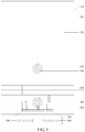
- the display panel may include a flexible substrate 110 including a bending area 104 and a first substrate area 102 and a second substrate area 106 respectively disposed at two sides of the bending area 104; a display area 120, disposed in the first substrate area 102 and including a plurality of sub-pixels and a fingerprint sensing area 130, the fingerprint sensing area 130 including a photic hole 140 and a light-emitting unit; a fingerprint imaging area 160 disposed in the second substrate area 106, and aligned with the fingerprint sensing area 130 after the bending area 104 is bent, and configured to receive an optical signal emitted by the light emitting unit, reflected by a fingerprint and passing through the photic hole 140, and convert the optical signal into an electrical signal; and a fingerprint recognition circuit 180 coupled to the fingerprint sensing area 160 and configured to generate a corresponding fingerprint image signal based on the electrical signal output by the fingerprint imaging area 160.
- the display area including the fingerprint sensing area and the fingerprint imaging area are disposed on the same flexible substrate, and the fingerprint imaging area can be made aligned with the fingerprint sensing area after the bending area is bent, which can increase the integration degree of the display panel and make the display panel lighter and thinner.
- the fingerprint imaging area can be made aligned with the fingerprint sensing area after the bending area is bent, which can increase the integration degree of the display panel and make the display panel lighter and thinner.
- by converting an optical signal reflected by a fingerprint and passing through the hole into an electrical signal in the fingerprint imaging area, and processing the electrical signal to form a fingerprint image signal by the fingerprint recognition circuit it can implement fingerprint recognition based on the principle of pinhole imaging.
- the manufacturing process can be simplified and the manufacturing cost can be reduced.
- the flexible substrate 110 is a transparent flexible substrate, and the flexible substrate 110 includes a bending area 104 and a first substrate area 102 above the bending area 104 and a second substrate area 106 below the bending area 104 respectively.
- a display area 120 is disposed on the first substrate area 102.
- the display area 120 includes a plurality of sub-pixels for displaying.
- a fingerprint sensing area 130 is further disposed in the display area 120.
- the fingerprint sensing area 130 includes a plurality of photic holes 140 and a light emitting unit, and the light emitting unit is configured to provide a light source for fingerprint recognition.
- the plurality of photic holes 140 may not actually through holes penetrating the transparent flexible substrate, but may represent transparent areas or blank areas in which the light rays can pass freely in the fingerprint sensing area 130, that is, the photic holes 140 are transparent areas distributed outside the area where the sub-pixels are disposed.
- the purpose of providing the photic holes 140 is to utilize the principle of pinhole imaging to implement imaging. Since the aperture of the photic hole 140 is small, the image information collected through the photic hole 140 is relatively large, and the photic holes 140 do not affect the normal display of the display area.
- the light emitting unit of the fingerprint sensing area 130 may also be an OLED or a QLED correspondingly, but the exemplary embodiment of the present disclosure is not limited thereto, and the light emitting unit in the fingerprint sensing area 130 may also be other suitable light sources, such as a point light source specially arranged in the display panel, which is also within the scope of the present disclosure.
- the fingerprint imaging area 160 is disposed on the second substrate area 106 below the bending area 104 and can be aligned with the fingerprint sensing area 130 after the bending area 104 is bent.
- the fingerprint imaging area 160 includes a plurality of photoelectric conversion units configured to receive an optical signal emitted by the light emitting unit, reflected by a fingerprint and passing through the photic hole 140 and convert the optical signal into an electrical signal.
- the second substrate area 106 is also connected (e.g., electrically connected) to the flexible circuit board 170, and the flexible circuit board 170 is provided with a fingerprint recognition circuit 180 and a display driving circuit 190.
- the fingerprint recognition circuit 180 is connected (e.g., electrically connected) to the fingerprint sensing area 160 and configured to generate a corresponding fingerprint image signal based on the electrical signal output by the fingerprint imaging area 160.
- the display driving circuit 190 is connected (e.g., electrically connected) to the display area 120, and configured to drive a plurality of sub-pixels in the display area 120 for display. As shown in FIG. 1 , the circuit lines of the display area 120 are connected (e.g., electrically connected) to the flexible circuit board 170 and the display driving circuit 190 bypassing the fingerprint imaging area 160.
- each of the shape of the fingerprint sensing area 130 and the shape of the fingerprint imaging area 160 shown in FIG. 1 is circular, but the exemplary embodiment of the present disclosure is not limited thereto.
- the shape of the fingerprint sensing area 130 and the shape of the fingerprint imaging area 160 may also be a shape such as a rectangle or an ellipse, which is not specifically limited in the present disclosure.
- the bending area 104 can be bent along a dashed line in the middle of the bending area 104.
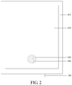
- FIG. 2 illustrates a front view of the display panel after the bending area 104 is bent. In FIG. 2 , the fingerprint imaging area 160 is disposed rearward of and aligned with the fingerprint sensing area 130.
- the fingerprint sensing area 130 may coincide with the fingerprint imaging area 160.
- the area of the fingerprint imaging area 160 may be provided as larger than the area of the fingerprint sensing area 130. That is, the area of the fingerprint imaging area 160 is larger than or equal to the area of the fingerprint sensing area 130.
- the first substrate area 102 and the second substrate area 106 are connected to each other via the bending area 104, and the fingerprint sensing area 130 is made aligned with the fingerprint imaging area 160 when the bending area 104 is bent.
- the present disclosure is not limited thereto, and in other embodiments of the present disclosure, the bending area 104 may be omitted.
- the first substrate area 102 and the second substrate area 106 may be divided into separate substrates along a dashed line in the middle of the bending area 104, and the two separate substrates may be overlapped to make the fingerprint sensing area 130 aligned with the fingerprint imaging area 160.
- the first substrate area 102 and the second substrate area 106 may also be fabricated separately, and the separately fabricated substrates may be overlapped to make the fingerprint sensing area 130 aligned with the fingerprint imaging area 160.
- the first substrate area 102 and the second substrate area 106 may be connected to each other through a FPC (flexible circuit board), vias, connection terminals, and the like.
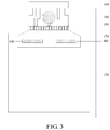
- FIG. 3 illustrates a schematic rear view of the display panel after the first substrate area 102 and the second substrate area 106 are bent.
- fingerprint imaging area 160 is formed in the second substrate area 106 of the flexible substrate.
- the fingerprint imaging area 160 may be formed by exposure development etching together with the plurality of sub-pixels of the display area 120.
- the fingerprint imaging area 160 includes a plurality of tiny photoelectric conversion units.
- the photoelectric conversion units are disposed corresponding to the photic holes 140 in the fingerprint sensing area 130 and configured to collect optical signals that pass through the photic holes 140 after being reflected by a fingerprint.
- the photoelectric conversion unit can convert the collected optical signal into an electrical signal and output the electrical signal to the fingerprint recognition circuit 180.
- the circuit lines of the photoelectric conversion units of the fingerprint imaging area 160 are connected to the flexible circuit board 170 and the fingerprint recognition circuit 180.
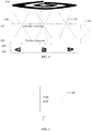
- FIG. 4 illustrates a stacked structure diagram of the fingerprint sensing area 130 and the fingerprint imaging area 140 according to an exemplary embodiment of the present disclosure.
- a plurality of sub-pixels 420 are formed above the fingerprint sensing area 130 on the first substrate area 102.
- the plurality of sub-pixels 420 may be active light emitting units such as OLEDs or QLEDs. That is, the plurality of sub-pixels 420 may be used as a light source for fingerprint recognition.
- Blank areas between the plurality of sub-pixels 420 may be formed as the photic holes 140, and each of the photic holes 140 is disposed corresponding to one of the plurality of photoelectric conversion units 430 below the second substrate area 106 to form a fingerprint information collecting module.
- the plurality of photoelectric conversion units 430 and the plurality of sub-pixels 420 may be molded together on the flexible substrate. That is, at least a part of the film layers of the photoelectric conversion units 430 and the sub-pixels 420 may be formed in the same patterning process. Therefore, after the bending area 104 is bent, the photoelectric conversion units 430 are disposed below the flexible substrate.
- the light emitted by the plurality of sub-pixels 420 is reflected by a fingerprint 410, and is irradiated onto the photoelectric conversion units 430 through the photic holes 140.
- the photoelectric conversion unit 430 converts the optical signal including the fingerprint information based on the pinhole imaging into an electrical signal.
- the electrical signal is subject to image synthesis processing 440 by the fingerprint recognition circuit 180 to synthesize the images of the respective photic holes 140 into fingerprint image information.
- the image synthesis processing 440 the three-part image signal including the partial fingerprint information formed by the three photic holes 140 is processed, to synthesis the three pieces of partial fingerprint information to form a fingerprint image signal corresponding to the fingerprint 410.
- FIG. 5 illustrates a schematic diagram of a photoelectric conversion principle according to the present exemplary embodiment.
- the photoelectric characteristics of photons that increase the semiconductor mobility that is, the excitation of photons causing the current of the photoelectric conversion unit 430 to change is utilized.
- the current change is fed back to the fingerprint recognition circuit 180.
- the fingerprint recognition circuit 180 performs the image synthesis processing 440 on the electrical signal from each photoelectric conversion unit 430 which corresponds to the optical signal, to form a fingerprint image signal corresponding to the fingerprint 410 for fingerprint recognition.
- the material of the photoelectric conversion unit includes a material such as a P-Si semiconductor, an a-Si semiconductor, or an IGZO semiconductor, which is not specifically limited in the present disclosure.
- a manufacturing method of a display panel is also provided.
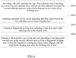
- the manufacturing method of a display panel may include the following steps S610-S640.
- Step S610 a flexible substrate having a first substrate area, a bending area, and a second substrate area is provided, wherein the first substrate area and the second substrate area are respectively disposed at two sides of the bending area.
- Step S620 a plurality of sub-pixels including thin film transistors are formed in the first substrate area to form a display area.
- Step S630 a fingerprint sensing area including a photic hole and a light emitting unit is formed in the display area.
- Step S640 a photoelectric conversion unit corresponding to the fingerprint sensing area is formed in the second substrate area to form a fingerprint imaging area, so that the fingerprint sensing area is aligned with the fingerprint imaging area after the bending area is bent.
- the photoelectric conversion units and at least a part of the film layers of the thin film transistors are formed in the same patterning process.
- the first substrate area 102 and the second substrate area 106 are connected to each other via the bending area 104, and the fingerprint sensing area 130 is made aligned with the fingerprint imaging area 160 when the bending area 104 is bent.
- the present disclosure is not limited thereto, and in other embodiments of the present disclosure, the bending area 104 may be omitted.
- the first substrate area 102 and the second substrate area 106 may be divided into separate substrates along a dashed line in the middle of the bending area 104, and the two separate substrates may be overlapped to make the fingerprint sensing area 130 aligned with the fingerprint imaging area 160.
- the first substrate area 102 and the second substrate area 106 may also be fabricated separately, and the separately fabricated substrates may be overlapped to make the fingerprint sensing area 130 aligned with the fingerprint imaging area 160.
- the first substrate area 102 and the second substrate area 106 may be connected to each other through a FPC (flexible circuit board), vias, connection terminals, and the like.
- the display area including the fingerprint sensing area and the fingerprint imaging area are disposed on the same flexible substrate, and the fingerprint imaging area can be made aligned with the fingerprint sensing area after the bending area is bent, which can increase the integration degree of the display panel and make the display panel lighter and thinner.
- the manufacturing process can be simplified and the manufacturing cost can be reduced.
- the photoelectric conversion units and at least a part of the film layers of the thin film transistors are formed in the same patterning process, which may include: a semiconductor material layer of the photoelectric conversion unit and a partial film layer of the thin film transistor of the display, such as an active layer are formed in the same patterning process.
- a semiconductor material layer of the photoelectric conversion unit is P-Si (polycrystalline-Si, polysilicon)
- the thin film transistor of the display area is a P-Si TFT (Thin Film Transistor)
- the P-Si film layer of the photoelectric conversion unit can be formed in the same patterning process as the active layer of the P-Si TFT.
- the a-Si film layer of the photoelectric conversion unit can be formed in the same patterning process as the a-Si film layer of the a-Si TFT.
- the material of the photoelectric conversion unit is IGZO (Indium Gallium Zinc Oxide)
- the thin film transistor of the display area is an IGZO TFT
- the IGZO film layer of the photoelectric conversion unit can be formed in the same patterning process as the IGZO layer of the IGZO TFT.
- other film layers of the photoelectric conversion unit such as metal layers, can also be formed in the same patterning process as the metal layers in the thin film transistor, which are all within the scope of the present disclosure.
- the light emitting unit includes a plurality of the sub-pixels.
- the photic hole includes a transparent area distributed outside the area where the sub-pixels are disposed.
- the material of the photoelectric conversion unit includes a P-Si semiconductor, an a-Si semiconductor, or an IGZO semiconductor.
- the area of the fingerprint imaging area is larger than or equal to the area of the fingerprint sensing area.
- the light emitting unit is an OLED unit or a QLED unit.
- a driving method of a display panel is further provided for driving the display panel in the above exemplary embodiments, and the driving method may include:
- the display device including the display panel according to the above embodiments. Since the display device in the exemplary embodiment of the present disclosure employs the above display panel, it has at least all the advantages corresponding to the display panel.
- the display device may be: an OLED display device, a mobile phone, a tablet computer, a television, a display, a notebook computer, a digital camera, and the like, or any product or component having a display function, which is not specifically limited by the present disclosure.
Landscapes
- Engineering & Computer Science (AREA)
- Theoretical Computer Science (AREA)
- Physics & Mathematics (AREA)
- General Physics & Mathematics (AREA)
- Computer Security & Cryptography (AREA)
- Multimedia (AREA)
- Human Computer Interaction (AREA)
- Computer Hardware Design (AREA)
- Software Systems (AREA)
- General Engineering & Computer Science (AREA)
- Devices For Indicating Variable Information By Combining Individual Elements (AREA)
- Electroluminescent Light Sources (AREA)
- Image Input (AREA)
Abstract
Description
- The present application claims priority of Chinese patent application No.
201710743103.0, filed on August 25, 2017 - The present disclosure relates to the field of display technology, and more particularly to a display device, a display panel, a manufacturing method thereof, and a driving method thereof.
- At present, fingerprint recognition technology has been widely used in various smart terminals. Since the fingerprint recognition function provides more convenience and security for people to operate smart terminals, it has gradually become an indispensable function in various intelligent terminals.
- In the existing display technology scheme for integrated fingerprint recognition, the fingerprint recognition area is disposed at the lower part or the rear part of the display area. The fingerprint recognition area is provided with a fingerprint recognition sensor, and the fingerprint recognition sensor is connected with an external fingerprint recognition circuit. When the finger touches in the fingerprint recognition area, the fingerprint recognition sensor sends the collected fingerprint information to the fingerprint recognition circuit, and the fingerprint recognition circuit processes the fingerprint information to implement the fingerprint recognition function.
- It should be noted that the information disclosed in the Background section above is only for enhancement of understanding of the background of the present disclosure, and thus may include information that does not constitute prior art known to those of ordinary skill in the art.
- According to one aspect of the present disclosure, there is provided a display panel, including:
- a flexible substrate including a bending area and a first substrate area and a second substrate area respectively disposed on two sides of the bending area;
- a display area disposed in the first substrate area and includes a plurality of sub-pixels and a fingerprint sensing area, the fingerprint sensing area including a photic hole and a light-emitting unit;
- a fingerprint imaging area disposed in the second substrate area and capable of being aligned with the fingerprint sensing area after the bending area is bent, and configured to receive an optical signal emitted by the light emitting unit, reflected by a fingerprint and passing through the photic hole, and convert the optical signal to an electrical signal; and
- a fingerprint recognition circuit connected to the fingerprint sensing area and configured to generate a corresponding fingerprint image signal based on the electrical signal output by the fingerprint imaging area.
- In an exemplary embodiment of the present disclosure, the light emitting unit includes a plurality of the sub-pixels.
- In an exemplary embodiment of the present disclosure, the photic hole includes a transparent area distributed around a periphery of an area where the sub-pixels are disposed in the display area.
- In an exemplary embodiment of the present disclosure, the fingerprint imaging area includes a photoelectric conversion unit, and photoelectric conversion unit includes polysilicon, amorphous silicon or indium gallium zinc oxide.
- In an exemplary embodiment of the present disclosure, the fingerprint recognition circuit is disposed on a flexible circuit board.
- In an exemplary embodiment of the present disclosure, an area of the fingerprint imaging area is larger than or equal to an area of the fingerprint sensing area.
- In an exemplary embodiment of the present disclosure, the light emitting unit is an organic light emitting diode unit or a quantum dot light emitting unit.
- In an exemplary embodiment of the present disclosure, each of a shape of the fingerprint sensing area and a shape of the fingerprint imaging area includes one of a circle, a rectangle, or an ellipse.
- According to one aspect of the present disclosure, there is provided a display device including any of the display panel described above.
- According to one aspect of the present disclosure, there is provided a manufacturing method of a display panel, including:
- providing a flexible substrate having a first substrate area, a bending area, and a second substrate area, wherein the first substrate area and the second substrate area are respectively disposed at two sides of the bending area;
- forming a plurality of sub-pixels including thin film transistors in the first substrate area to form a display area;
- forming a fingerprint sensing area including a photic hole and a light emitting unit in the display area; and
- forming a photoelectric conversion unit corresponding to the fingerprint sensing area in the second substrate area to form a fingerprint imaging area, so that the fingerprint sensing area is aligned with the fingerprint imaging area after the bending area is bent.
- In an exemplary embodiment of the present disclosure, the photoelectric conversion unit and at least a part of the film layers of the thin film transistors are formed in the same patterning process.
- In an exemplary embodiment of the present disclosure, the light emitting unit includes a plurality of sub-pixels.
- In an exemplary embodiment of the present disclosure, the photic hole includes a transparent area distributed outside an area where the sub-pixels are disposed.
- According to one aspect of the present disclosure, there is provided a driving method of a display panel, for driving any of the display panel described above, wherein the driving method includes:
- providing a driving signal to the light emitting unit to drive the light emitting unit to emit light;
- receiving, by the fingerprint imaging area, an optical signal emitted by the light emitting unit, reflected by a fingerprint and passing through the photic hole, and converting the optical signal into an electrical signal; and
- generating a corresponding fingerprint image signal by the fingerprint recognition circuit based on the electrical signal.
- According to one aspect of the present disclosure, there is provided a fingerprint recognition substrate including:
- a substrate including a bending area and a first substrate area and a second substrate area respectively disposed at two sides of the bending area;
- a fingerprint sensing area disposed in the first substrate area, the fingerprint sensing area including a photic hole; and
- a fingerprint imaging area, disposed in the second substrate area,
- wherein after the bending area is bent, an orthographic projection of the fingerprint sensing area on the second substrate area at least partially overlaps with the fingerprint imaging area, and the fingerprint imaging area is configured to receive an optical signal reflected by a fingerprint and passing through the photic hole, and convert the optical signal into an electrical signal.
- In an exemplary embodiment of the present disclosure, the fingerprint recognition substrate further includes a light emitting unit, wherein an optical signal emitted by the light emitting unit is received by the fingerprint imaging area through the photic hole after the optical signal is reflected by a fingerprint.
- In an exemplary embodiment of the present disclosure, the fingerprint imaging area includes a photoelectric conversion unit, and the photoelectric conversion unit includes polysilicon, amorphous silicon or indium gallium zinc oxide.
- In an exemplary embodiment of the present disclosure, the fingerprint recognition circuit is disposed on a flexible circuit board.
- In an exemplary embodiment of the present disclosure, an area of the fingerprint imaging area is larger than or equal to an area of the fingerprint sensing area.
- In an exemplary embodiment of the present disclosure, the light emitting unit is an organic light emitting diode unit or a quantum dot light emitting unit.
- In an exemplary embodiment of the present disclosure, each of a shape of the fingerprint sensing area and a shape of the fingerprint imaging area includes one or more of a circle, a rectangle, or an ellipse.
- According to one aspect of the present disclosure, there is provided a manufacturing method of a display panel, including:
- providing a flexible substrate having a first substrate area, a bending area, and a second substrate area, wherein the first substrate area and the second substrate area are respectively located at two sides of the bending area;
- forming a fingerprint sensing area including a photic hole in the first substrate area;
- forming a fingerprint imaging area in the second substrate area, such that after the bending area is bent, an orthographic projection of the fingerprint sensing area on the second substrate area at least partially overlaps the fingerprint imaging area,
- wherein the fingerprint imaging area is configured to receive an optical signal through the photic hole after the optical signal is reflected by a fingerprint, and convert the optical signal into an electrical signal.
- In an exemplary embodiment of the present disclosure, the manufacturing method of a display panel further includes forming a light emitting unit, wherein an optical signal emitted by the light emitting unit is received by the fingerprint imaging area through the photic hole after the optical signal is reflected by a fingerprint.
- In an exemplary embodiment of the present disclosure, an area of the fingerprint imaging area is larger than or equal to an area of the fingerprint sensing area.
- It should be understood that the above general description and the following detailed description are intended to be illustrative and not restrictive.
- The accompanying drawings, which are incorporated in and constitute a part of this specification, illustrate embodiments consistent with the present disclosure and, together with the description, serve to explain the principles of the present disclosure. It is apparent that the drawings in the following description are only some of the embodiments of the present disclosure, and other drawings may be obtained by those skilled in the art from these drawings without paying creative effort.
-
FIG. 1 illustrates a schematic diagram of a display panel according to an exemplary embodiment of the present disclosure; -
FIG. 2 illustrates a front view of the display panel shown inFIG. 1 after being bent; -
FIG. 3 illustrates a schematic rear view of the display panel shown inFIG. 1 after being bent; -
FIG. 4 illustrates a schematic structural diagram of a fingerprint sensing area and a fingerprint imaging area according to an illustrative example of the present disclosure; -
FIG. 5 illustrates a schematic diagram of a principle of a photoelectric conversion unit according to an exemplary embodiment of the present disclosure; and -
FIG. 6 illustrates a flow chart of a manufacturing method of a display panel according to an exemplary embodiment of the present disclosure. - Exemplary embodiments will now be described more fully with reference to the accompanying drawings. However, the exemplary embodiments can be embodied in a variety of forms and should not be construed as being limited to the examples set forth herein; rather, these embodiments are provided to make the present disclosure to be more complete and thorough, to fully convey the concept of the exemplary embodiments to those skilled in the art. The described features, structures, or characteristics may be combined in any suitable manner in one or more embodiments. In the following description, numerous specific details are set forth to provide a thorough understanding of the embodiments of the present disclosure. However, one skilled in the art will appreciate that one or more of the specific details may be omitted or other methods, components, devices, steps, etc. may be employed. In other instances, well-known technical solutions are not shown or described in detail to avoid obscuring aspects of the present disclosure.
- In addition, the drawings are merely schematic representations of the present disclosure and are not necessarily drawn to scale. The same reference numerals in the drawings denote the same or similar parts, and the repeated description thereof will be omitted. Some of the block diagrams shown in the figures are functional entities and do not necessarily have to correspond to physically or logically separate entities. These functional entities may be implemented in software, or implemented in one or more hardware modules or integrated circuits, or implemented in different network and/or processor devices and/or microcontroller devices.
- In an exemplary embodiment of the present disclosure, a display panel is first provided. Referring to
FIG. 1 , the display panel may include aflexible substrate 110 including abending area 104 and afirst substrate area 102 and asecond substrate area 106 respectively disposed at two sides of thebending area 104; adisplay area 120, disposed in thefirst substrate area 102 and including a plurality of sub-pixels and afingerprint sensing area 130, thefingerprint sensing area 130 including aphotic hole 140 and a light-emitting unit; afingerprint imaging area 160 disposed in thesecond substrate area 106, and aligned with thefingerprint sensing area 130 after thebending area 104 is bent, and configured to receive an optical signal emitted by the light emitting unit, reflected by a fingerprint and passing through thephotic hole 140, and convert the optical signal into an electrical signal; and afingerprint recognition circuit 180 coupled to thefingerprint sensing area 160 and configured to generate a corresponding fingerprint image signal based on the electrical signal output by thefingerprint imaging area 160. - In the display panel according to the exemplary embodiment of the present disclosure, on the one hand, the display area including the fingerprint sensing area and the fingerprint imaging area are disposed on the same flexible substrate, and the fingerprint imaging area can be made aligned with the fingerprint sensing area after the bending area is bent, which can increase the integration degree of the display panel and make the display panel lighter and thinner. On the other hand, by converting an optical signal reflected by a fingerprint and passing through the hole into an electrical signal in the fingerprint imaging area, and processing the electrical signal to form a fingerprint image signal by the fingerprint recognition circuit, it can implement fingerprint recognition based on the principle of pinhole imaging. On yet another hand, since at least part of the film layers of the display area and the fingerprint imaging area can be formed in the same patterning process, the manufacturing process can be simplified and the manufacturing cost can be reduced.
- Hereinafter, the display panel in the exemplary embodiment of the present disclosure will be described in detail.
- Referring to
FIG. 1 , in the exemplary embodiment of the present disclosure, theflexible substrate 110 is a transparent flexible substrate, and theflexible substrate 110 includes abending area 104 and afirst substrate area 102 above the bendingarea 104 and asecond substrate area 106 below the bendingarea 104 respectively. Adisplay area 120 is disposed on thefirst substrate area 102. Thedisplay area 120 includes a plurality of sub-pixels for displaying. Afingerprint sensing area 130 is further disposed in thedisplay area 120. Thefingerprint sensing area 130 includes a plurality ofphotic holes 140 and a light emitting unit, and the light emitting unit is configured to provide a light source for fingerprint recognition. The plurality ofphotic holes 140 may not actually through holes penetrating the transparent flexible substrate, but may represent transparent areas or blank areas in which the light rays can pass freely in thefingerprint sensing area 130, that is, thephotic holes 140 are transparent areas distributed outside the area where the sub-pixels are disposed. The purpose of providing thephotic holes 140 is to utilize the principle of pinhole imaging to implement imaging. Since the aperture of thephotic hole 140 is small, the image information collected through thephotic hole 140 is relatively large, and thephotic holes 140 do not affect the normal display of the display area. - It should be noted that, in an exemplary embodiment of the present disclosure, when the plurality of sub-pixels are Organic Light-Emitting Diodes (OLEDs) or Quantum Dot Light Emitting Diodes (QLEDs), the light emitting unit of the
fingerprint sensing area 130 may also be an OLED or a QLED correspondingly, but the exemplary embodiment of the present disclosure is not limited thereto, and the light emitting unit in thefingerprint sensing area 130 may also be other suitable light sources, such as a point light source specially arranged in the display panel, which is also within the scope of the present disclosure. - Still referring to
FIG. 1 , thefingerprint imaging area 160 is disposed on thesecond substrate area 106 below the bendingarea 104 and can be aligned with thefingerprint sensing area 130 after thebending area 104 is bent. Thefingerprint imaging area 160 includes a plurality of photoelectric conversion units configured to receive an optical signal emitted by the light emitting unit, reflected by a fingerprint and passing through thephotic hole 140 and convert the optical signal into an electrical signal. In addition, thesecond substrate area 106 is also connected (e.g., electrically connected) to theflexible circuit board 170, and theflexible circuit board 170 is provided with afingerprint recognition circuit 180 and adisplay driving circuit 190. Thefingerprint recognition circuit 180 is connected (e.g., electrically connected) to thefingerprint sensing area 160 and configured to generate a corresponding fingerprint image signal based on the electrical signal output by thefingerprint imaging area 160. Thedisplay driving circuit 190 is connected (e.g., electrically connected) to thedisplay area 120, and configured to drive a plurality of sub-pixels in thedisplay area 120 for display. As shown inFIG. 1 , the circuit lines of thedisplay area 120 are connected (e.g., electrically connected) to theflexible circuit board 170 and thedisplay driving circuit 190 bypassing thefingerprint imaging area 160. - It should be noted that, in an exemplary embodiment of the exemplary embodiment, each of the shape of the
fingerprint sensing area 130 and the shape of thefingerprint imaging area 160 shown inFIG. 1 is circular, but the exemplary embodiment of the present disclosure is not limited thereto. For example, the shape of thefingerprint sensing area 130 and the shape of thefingerprint imaging area 160 may also be a shape such as a rectangle or an ellipse, which is not specifically limited in the present disclosure. Further, the bendingarea 104 can be bent along a dashed line in the middle of thebending area 104.FIG. 2 illustrates a front view of the display panel after thebending area 104 is bent. InFIG. 2 , thefingerprint imaging area 160 is disposed rearward of and aligned with thefingerprint sensing area 130. In an exemplary embodiment of the present disclosure, after thebending area 104 is bent, thefingerprint sensing area 130 may coincide with thefingerprint imaging area 160. In particular, in order to ensure that thefingerprint imaging area 160 can completely receive the light passing through the photic holes in thefingerprint sensing area 130, the area of thefingerprint imaging area 160 may be provided as larger than the area of thefingerprint sensing area 130. That is, the area of thefingerprint imaging area 160 is larger than or equal to the area of thefingerprint sensing area 130. - In addition, it should also be understood that in the embodiment, the
first substrate area 102 and thesecond substrate area 106 are connected to each other via thebending area 104, and thefingerprint sensing area 130 is made aligned with thefingerprint imaging area 160 when thebending area 104 is bent. However, the present disclosure is not limited thereto, and in other embodiments of the present disclosure, the bendingarea 104 may be omitted. For example, in one embodiment, thefirst substrate area 102 and thesecond substrate area 106 may be divided into separate substrates along a dashed line in the middle of thebending area 104, and the two separate substrates may be overlapped to make thefingerprint sensing area 130 aligned with thefingerprint imaging area 160. In other embodiments of the present disclosure, thefirst substrate area 102 and thesecond substrate area 106 may also be fabricated separately, and the separately fabricated substrates may be overlapped to make thefingerprint sensing area 130 aligned with thefingerprint imaging area 160. In the case where thefirst substrate area 102 and thesecond substrate area 106 are separate substrates, thefirst substrate area 102 and thesecond substrate area 106 may be connected to each other through a FPC (flexible circuit board), vias, connection terminals, and the like. -
FIG. 3 illustrates a schematic rear view of the display panel after thefirst substrate area 102 and thesecond substrate area 106 are bent. InFIG. 3 ,fingerprint imaging area 160 is formed in thesecond substrate area 106 of the flexible substrate. Thefingerprint imaging area 160 may be formed by exposure development etching together with the plurality of sub-pixels of thedisplay area 120. Thefingerprint imaging area 160 includes a plurality of tiny photoelectric conversion units. The photoelectric conversion units are disposed corresponding to thephotic holes 140 in thefingerprint sensing area 130 and configured to collect optical signals that pass through thephotic holes 140 after being reflected by a fingerprint. The photoelectric conversion unit can convert the collected optical signal into an electrical signal and output the electrical signal to thefingerprint recognition circuit 180. The circuit lines of the photoelectric conversion units of thefingerprint imaging area 160 are connected to theflexible circuit board 170 and thefingerprint recognition circuit 180. - Further,
FIG. 4 illustrates a stacked structure diagram of thefingerprint sensing area 130 and thefingerprint imaging area 140 according to an exemplary embodiment of the present disclosure. InFIG. 4 , a plurality ofsub-pixels 420 are formed above thefingerprint sensing area 130 on thefirst substrate area 102. The plurality ofsub-pixels 420 may be active light emitting units such as OLEDs or QLEDs. That is, the plurality ofsub-pixels 420 may be used as a light source for fingerprint recognition. Blank areas between the plurality ofsub-pixels 420 may be formed as thephotic holes 140, and each of thephotic holes 140 is disposed corresponding to one of the plurality ofphotoelectric conversion units 430 below thesecond substrate area 106 to form a fingerprint information collecting module. The plurality ofphotoelectric conversion units 430 and the plurality ofsub-pixels 420 may be molded together on the flexible substrate. That is, at least a part of the film layers of thephotoelectric conversion units 430 and the sub-pixels 420 may be formed in the same patterning process. Therefore, after thebending area 104 is bent, thephotoelectric conversion units 430 are disposed below the flexible substrate. - Still referring to
FIG. 4 , the light emitted by the plurality ofsub-pixels 420 is reflected by afingerprint 410, and is irradiated onto thephotoelectric conversion units 430 through thephotic holes 140. Thephotoelectric conversion unit 430 converts the optical signal including the fingerprint information based on the pinhole imaging into an electrical signal. Then, the electrical signal is subject toimage synthesis processing 440 by thefingerprint recognition circuit 180 to synthesize the images of the respectivephotic holes 140 into fingerprint image information. Taking the three-part fingerprint image collected from the three photic holes inFIG. 4 as an example, in theimage synthesis processing 440, the three-part image signal including the partial fingerprint information formed by the threephotic holes 140 is processed, to synthesis the three pieces of partial fingerprint information to form a fingerprint image signal corresponding to thefingerprint 410. -
FIG. 5 illustrates a schematic diagram of a photoelectric conversion principle according to the present exemplary embodiment. As shown inFIG. 5 , the photoelectric characteristics of photons that increase the semiconductor mobility, that is, the excitation of photons causing the current of thephotoelectric conversion unit 430 to change is utilized. The current change is fed back to thefingerprint recognition circuit 180. Thefingerprint recognition circuit 180 performs theimage synthesis processing 440 on the electrical signal from eachphotoelectric conversion unit 430 which corresponds to the optical signal, to form a fingerprint image signal corresponding to thefingerprint 410 for fingerprint recognition. In an exemplary embodiment of the present disclosure, the material of the photoelectric conversion unit includes a material such as a P-Si semiconductor, an a-Si semiconductor, or an IGZO semiconductor, which is not specifically limited in the present disclosure. - Further, in another exemplary embodiment of the present disclosure, a manufacturing method of a display panel is also provided. Referring to
FIG. 6 , the manufacturing method of a display panel may include the following steps S610-S640. - In Step S610, a flexible substrate having a first substrate area, a bending area, and a second substrate area is provided, wherein the first substrate area and the second substrate area are respectively disposed at two sides of the bending area.
- In Step S620, a plurality of sub-pixels including thin film transistors are formed in the first substrate area to form a display area.
- In Step S630, a fingerprint sensing area including a photic hole and a light emitting unit is formed in the display area.
- In Step S640, a photoelectric conversion unit corresponding to the fingerprint sensing area is formed in the second substrate area to form a fingerprint imaging area, so that the fingerprint sensing area is aligned with the fingerprint imaging area after the bending area is bent.
- In the embodiment, the photoelectric conversion units and at least a part of the film layers of the thin film transistors are formed in the same patterning process.
- In addition, it should also be understood that in the present embodiment, the
first substrate area 102 and thesecond substrate area 106 are connected to each other via thebending area 104, and thefingerprint sensing area 130 is made aligned with thefingerprint imaging area 160 when thebending area 104 is bent. However, the present disclosure is not limited thereto, and in other embodiments of the present disclosure, the bendingarea 104 may be omitted. For example, in one embodiment, thefirst substrate area 102 and thesecond substrate area 106 may be divided into separate substrates along a dashed line in the middle of thebending area 104, and the two separate substrates may be overlapped to make thefingerprint sensing area 130 aligned with thefingerprint imaging area 160. In other embodiments of the present disclosure, thefirst substrate area 102 and thesecond substrate area 106 may also be fabricated separately, and the separately fabricated substrates may be overlapped to make thefingerprint sensing area 130 aligned with thefingerprint imaging area 160. In the case where thefirst substrate area 102 and thesecond substrate area 106 are separate substrates, thefirst substrate area 102 and thesecond substrate area 106 may be connected to each other through a FPC (flexible circuit board), vias, connection terminals, and the like. - In the manufacturing method of a display panel according to the exemplary embodiment of the present disclosure, on the one hand, the display area including the fingerprint sensing area and the fingerprint imaging area are disposed on the same flexible substrate, and the fingerprint imaging area can be made aligned with the fingerprint sensing area after the bending area is bent, which can increase the integration degree of the display panel and make the display panel lighter and thinner. On the other hand, since at least part of the film layers of the thin film transistors and the photoelectric conversion units can be formed in the same patterning process, the manufacturing process can be simplified and the manufacturing cost can be reduced.
- In an exemplary embodiment of the present disclosure, the photoelectric conversion units and at least a part of the film layers of the thin film transistors are formed in the same patterning process, which may include: a semiconductor material layer of the photoelectric conversion unit and a partial film layer of the thin film transistor of the display, such as an active layer are formed in the same patterning process. For example, when the material of the photoelectric conversion unit is P-Si (polycrystalline-Si, polysilicon), and the thin film transistor of the display area is a P-Si TFT (Thin Film Transistor), the P-Si film layer of the photoelectric conversion unit can be formed in the same patterning process as the active layer of the P-Si TFT. When the material of the photoelectric conversion unit is a-Si (amorphous- Si, amorphous silicon), and the thin film transistor of the display area is an a-Si TFT, the a-Si film layer of the photoelectric conversion unit can be formed in the same patterning process as the a-Si film layer of the a-Si TFT. When the material of the photoelectric conversion unit is IGZO (Indium Gallium Zinc Oxide), and the thin film transistor of the display area is an IGZO TFT, the IGZO film layer of the photoelectric conversion unit can be formed in the same patterning process as the IGZO layer of the IGZO TFT. However, those skilled in the art will readily understand that other film layers of the photoelectric conversion unit, such as metal layers, can also be formed in the same patterning process as the metal layers in the thin film transistor, which are all within the scope of the present disclosure.
- Further, in an exemplary embodiment of the present disclosure, the light emitting unit includes a plurality of the sub-pixels.
- Further, in an exemplary embodiment of the present disclosure, the photic hole includes a transparent area distributed outside the area where the sub-pixels are disposed.
- Further, in an exemplary embodiment of the present disclosure, the material of the photoelectric conversion unit includes a P-Si semiconductor, an a-Si semiconductor, or an IGZO semiconductor.
- Further, in an exemplary embodiment of the present disclosure, the area of the fingerprint imaging area is larger than or equal to the area of the fingerprint sensing area.
- Further, in an exemplary embodiment of the present disclosure, the light emitting unit is an OLED unit or a QLED unit.
- In addition, in an exemplary embodiment of the present disclosure, a driving method of a display panel is further provided for driving the display panel in the above exemplary embodiments, and the driving method may include:
- providing a driving signal to the light emitting unit to drive the light emitting unit to emit light;
- receiving, by the fingerprint imaging area, an optical signal emitted by the light emitting unit, reflected by a fingerprint and passing through the photic hole, and converting the optical signal into an electrical signal; and
- generating a corresponding fingerprint image signal by the fingerprint recognition circuit based on the electrical signal.
- Since the specific implementation of the steps of the driving method has been described in detail in the description of the display panel in the above exemplary embodiments, it will not be repeated herein.
- Further, in an exemplary embodiment of the present disclosure, there is further provided a display device including the display panel according to the above embodiments. Since the display device in the exemplary embodiment of the present disclosure employs the above display panel, it has at least all the advantages corresponding to the display panel. In an exemplary embodiment, the display device may be: an OLED display device, a mobile phone, a tablet computer, a television, a display, a notebook computer, a digital camera, and the like, or any product or component having a display function, which is not specifically limited by the present disclosure.
- Other embodiments of the disclosure will be apparent to those skilled in the art from consideration of the specification and practice of the disclosure disclosed here. This application is intended to cover any variations, uses, or adaptations of the disclosure following the general principles thereof and including such departures from the present disclosure as come within known or customary practice in the art. It is intended that the specification and examples be considered as exemplary only, with a true scope and spirit of the disclosure being indicated by the appended claims.
- It will be appreciated that the present disclosure is not limited to the exact construction that has been described above and illustrated in the accompanying drawings, and that various modifications and changes can be made without departing from the scope thereof. It is intended that the scope of the disclosure only be limited by the appended claims.
Claims (20)
- A display panel, comprising:a flexible substrate comprising a bending area and a first substrate area and a second substrate area respectively disposed on two sides of the bending area;a display area disposed in the first substrate area and comprises a plurality of sub-pixels and a fingerprint sensing area, the fingerprint sensing area comprising a photic hole and a light-emitting unit;a fingerprint imaging area disposed in the second substrate area and capable of being aligned with the fingerprint sensing area after the bending area is bent, and configured to receive an optical signal emitted by the light emitting unit, reflected by a fingerprint and passing through the photic hole, and convert the optical signal to an electrical signal; anda fingerprint recognition circuit connected to the fingerprint sensing area and configured to generate a corresponding fingerprint image signal based on the electrical signal output by the fingerprint imaging area.
- The display panel according to claim 1, wherein the light emitting unit comprises a plurality of the sub-pixels.
- The display panel according to claim 1, wherein the photic hole comprises a transparent area distributed around a periphery of an area where the sub-pixels are disposed in the display area.
- The display panel according to claim 1, wherein the fingerprint imaging area comprises a photoelectric conversion unit, and the photoelectric conversion unit comprises polysilicon, amorphous silicon or indium gallium zinc oxide.
- The display panel according to claim 1, wherein the fingerprint recognition circuit is disposed on a flexible circuit board.
- The display panel according to any one of claims 1 to 5, wherein an area of the fingerprint imaging area is larger than or equal to an area of the fingerprint sensing area.
- The display panel according to claim 6, wherein the light emitting unit is an organic light emitting diode unit or a quantum dot light emitting unit.
- The display panel according to claim 6, wherein each of a shape of the fingerprint sensing area and a shape of the fingerprint imaging area comprises one or more of a circle, a rectangle, or an ellipse.
- A display device comprising the display panel according to any one of claims 1 to 8.
- A driving method of a display panel, for driving the display panel according to any one of claims 1 to 8, wherein the driving method comprises:providing a driving signal to the light emitting unit to drive the light emitting unit to emit light;receiving, by the fingerprint imaging area, an optical signal emitted by the light emitting unit, reflected by a fingerprint and passing through the photic hole, and converting the optical signal into an electrical signal; andgenerating a corresponding fingerprint image signal by the fingerprint recognition circuit based on the electrical signal.
- A fingerprint recognition substrate comprising:a substrate comprising a bending area and a first substrate area and a second substrate area respectively disposed at two sides of the bending area;a fingerprint sensing area disposed in the first substrate area, the fingerprint sensing area comprising a photic hole; anda fingerprint imaging area, disposed in the second substrate area,wherein after the bending area is bent, an orthographic projection of the fingerprint sensing area on the second substrate area at least partially overlaps with the fingerprint imaging area, and the fingerprint imaging area is configured to receive an optical signal reflected by a fingerprint and passing through the photic hole, and convert the optical signal into an electrical signal.
- The fingerprint recognition substrate according to claim 11, further comprising a light emitting unit, wherein an optical signal emitted by the light emitting unit is received by the fingerprint imaging area through the photic hole after the optical signal is reflected by a fingerprint.
- The fingerprint recognition substrate according to claim 11, wherein the fingerprint imaging area comprises a photoelectric conversion unit, and the photoelectric conversion unit comprises polysilicon, amorphous silicon or indium gallium zinc oxide.
- The fingerprint recognition substrate according to claim 11, wherein the fingerprint recognition circuit is disposed on a flexible circuit board.
- The fingerprint recognition substrate according to any one of claims 11 to 14, wherein an area of the fingerprint imaging area is larger than or equal to an area of the fingerprint sensing area.
- The fingerprint recognition substrate according to claim 15, wherein the light emitting unit is an organic light emitting diode unit or a quantum dot light emitting unit.
- The fingerprint recognition substrate according to claim 15, wherein each of a shape of the fingerprint sensing area and a shape of the fingerprint imaging area comprises one or more of a circle, a rectangle, or an ellipse.
- A manufacturing method of a display panel, comprising:providing a flexible substrate having a first substrate area, a bending area, and a second substrate area, wherein the first substrate area and the second substrate area are respectively located at two sides of the bending area;forming a fingerprint sensing area comprising a photic hole in the first substrate area;forming a fingerprint imaging area in the second substrate area, such that after the bending area is bent, an orthographic projection of the fingerprint sensing area on the second substrate area at least partially overlaps the fingerprint imaging area,wherein the fingerprint imaging area is configured to receive an optical signal through the photic hole after the optical signal is reflected by a fingerprint, and convert the optical signal into an electrical signal.
- The manufacturing method of a display panel according to claim 18, further comprising forming a light emitting unit, wherein an optical signal emitted by the light emitting unit is received by the fingerprint imaging area through the photic hole after the optical signal is reflected by a fingerprint.
- The manufacturing method of a display panel according to claim 18, wherein an area of the fingerprint imaging area is larger than or equal to an area of the fingerprint sensing area.
Applications Claiming Priority (2)
| Application Number | Priority Date | Filing Date | Title |
|---|---|---|---|
| CN201710743103.0A CN109426774B (en) | 2017-08-25 | 2017-08-25 | Display device, display panel, manufacturing method of display panel and driving method of display panel |
| PCT/CN2018/099995 WO2019037609A1 (en) | 2017-08-25 | 2018-08-10 | Display apparatus, and display panel and manufacturing method and drive method therefor |
Publications (3)
| Publication Number | Publication Date |
|---|---|
| EP3674966A1 true EP3674966A1 (en) | 2020-07-01 |
| EP3674966A4 EP3674966A4 (en) | 2021-05-26 |
| EP3674966B1 EP3674966B1 (en) | 2023-12-20 |
Family
ID=65438413
Family Applications (1)
| Application Number | Title | Priority Date | Filing Date |
|---|---|---|---|
| EP18847487.8A Active EP3674966B1 (en) | 2017-08-25 | 2018-08-10 | Display apparatus, and display panel and manufacturing method and drive method therefor |
Country Status (4)
| Country | Link |
|---|---|
| US (1) | US10915723B2 (en) |
| EP (1) | EP3674966B1 (en) |
| CN (1) | CN109426774B (en) |
| WO (1) | WO2019037609A1 (en) |
Families Citing this family (15)
| Publication number | Priority date | Publication date | Assignee | Title |
|---|---|---|---|---|
| CN108416280B (en) * | 2018-02-26 | 2021-09-17 | 厦门天马微电子有限公司 | Display module and display device |
| CN109638046B (en) * | 2018-12-07 | 2020-10-16 | 武汉华星光电半导体显示技术有限公司 | OLED display device with under-screen fingerprint recognition |
| JP7320970B2 (en) | 2019-03-28 | 2023-08-04 | 株式会社ジャパンディスプレイ | Display device |
| CN110136595A (en) * | 2019-05-17 | 2019-08-16 | 上海九山电子科技有限公司 | A kind of display panel and preparation method thereof, display device |
| CN110276312B (en) * | 2019-06-25 | 2021-08-13 | 上海天马有机发光显示技术有限公司 | A display panel and display device |
| CN110415612B (en) * | 2019-08-05 | 2022-07-08 | 京东方科技集团股份有限公司 | Display panel, electronic apparatus, and imaging method of display panel |
| US11281883B2 (en) | 2019-09-23 | 2022-03-22 | Novatek Microelectronics Corp. | Electronic circuit having fingerprint sensing function and method for sensing fingerprint image |
| CN110600523B (en) * | 2019-09-27 | 2021-08-03 | 武汉华星光电半导体显示技术有限公司 | A display panel and display device |
| CN110867165B (en) * | 2019-11-29 | 2021-10-15 | 厦门天马微电子有限公司 | Display panel and display device |
| TWI724723B (en) * | 2019-12-31 | 2021-04-11 | 義隆電子股份有限公司 | Fingerprint sensing device |
| KR102893632B1 (en) * | 2020-03-18 | 2025-12-01 | 삼성디스플레이 주식회사 | Display device |
| KR102970953B1 (en) * | 2020-08-12 | 2026-05-29 | 삼성디스플레이 주식회사 | Display device and method for driving the same |
| KR20220034265A (en) * | 2020-08-19 | 2022-03-18 | 삼성디스플레이 주식회사 | Display device and method of detecting fingerprint using the same |
| TWI764649B (en) * | 2021-03-26 | 2022-05-11 | 義隆電子股份有限公司 | Button module with vibration feedback and fingerprint sensing, fingerprint sensing module for the same, and control method for the same |
| CN113553944B (en) * | 2021-07-21 | 2024-09-13 | 京东方科技集团股份有限公司 | Display panel and display device |
Family Cites Families (10)
| Publication number | Priority date | Publication date | Assignee | Title |
|---|---|---|---|---|
| JP4743579B2 (en) * | 2004-06-01 | 2011-08-10 | カシオ計算機株式会社 | Image reading device |
| US8736587B2 (en) * | 2008-07-10 | 2014-05-27 | Semiconductor Energy Laboratory Co., Ltd. | Semiconductor device |
| CN104036172B (en) * | 2014-07-02 | 2017-08-08 | 南昌欧菲生物识别技术有限公司 | Fingerprint recognition detection components and its electronic installation |
| CN105786102A (en) * | 2014-12-26 | 2016-07-20 | 上海箩箕技术有限公司 | Mobile terminal with fingerprint recognition system |
| US10181070B2 (en) * | 2015-02-02 | 2019-01-15 | Synaptics Incorporated | Low profile illumination in an optical fingerprint sensor |
| KR102533171B1 (en) * | 2016-03-11 | 2023-05-18 | 삼성디스플레이 주식회사 | Flexible display device |
| CN106845451A (en) * | 2017-02-23 | 2017-06-13 | 上海理鑫光学科技有限公司 | A kind of optical system of fingerprint imaging |
| CN106847872B (en) * | 2017-03-24 | 2020-03-20 | 京东方科技集团股份有限公司 | Display device |
| KR102295068B1 (en) * | 2017-03-31 | 2021-08-31 | 삼성디스플레이 주식회사 | Display device and method of driving the display device |
| KR102452251B1 (en) * | 2017-08-04 | 2022-10-11 | 삼성디스플레이 주식회사 | Display apparatus |
-
2017
- 2017-08-25 CN CN201710743103.0A patent/CN109426774B/en active Active
-
2018
- 2018-08-10 EP EP18847487.8A patent/EP3674966B1/en active Active
- 2018-08-10 US US16/332,508 patent/US10915723B2/en active Active
- 2018-08-10 WO PCT/CN2018/099995 patent/WO2019037609A1/en not_active Ceased
Also Published As
| Publication number | Publication date |
|---|---|
| EP3674966A4 (en) | 2021-05-26 |
| WO2019037609A1 (en) | 2019-02-28 |
| US10915723B2 (en) | 2021-02-09 |
| CN109426774B (en) | 2022-05-03 |
| CN109426774A (en) | 2019-03-05 |
| US20190266379A1 (en) | 2019-08-29 |
| EP3674966B1 (en) | 2023-12-20 |
Similar Documents
| Publication | Publication Date | Title |
|---|---|---|
| EP3674966B1 (en) | Display apparatus, and display panel and manufacturing method and drive method therefor | |
| JP7128319B2 (en) | touch panel | |
| US11036958B2 (en) | Light emitting display panel and manufacture method thereof, display device | |
| US11009747B2 (en) | Backlight module and display device | |
| US11437358B2 (en) | Organic light emitting diode display device and method of manufacturing thereof | |
| CN108615019A (en) | A kind of display panel and display device | |
| CN112242427B (en) | Display devices | |
| US20210233962A1 (en) | Display Panel, Manufacturing Method Thereof, and Display Device | |
| CN105118840B (en) | Non-visible light flat-panel detector and preparation method thereof, image documentation equipment | |
| CN112054017B (en) | Display panel, preparation method and display device | |
| CN207800041U (en) | Display base plate and display device | |
| CN114093268B (en) | Curved display substrate, driving method and device thereof | |
| KR102949045B1 (en) | display panel and electric apparatus | |
| US10803279B2 (en) | Photosensitive component, display device and fingerprint identification method | |
| JP2025061191A (en) | Display device | |
| CN111653590B (en) | Display module assembly, display screen assembly and electronic equipment | |
| US20260114142A1 (en) | Display panel and electronic device | |
| CN120089064B (en) | Display module, method for manufacturing display module, and display device | |
| CN218831215U (en) | Display device | |
| KR20200115886A (en) | Display device | |
| US20260076073A1 (en) | Method of manufacturing display panel, display panel manufactured by using the method, and electronic apparatus including the display panel | |
| KR20240115966A (en) | Display device | |
| KR20260039871A (en) | Display panel and electronic apparatus comprising the same | |
| CN121646159A (en) | Display panel and electronic device comprising same |
Legal Events
| Date | Code | Title | Description |
|---|---|---|---|
| STAA | Information on the status of an ep patent application or granted ep patent |
Free format text: STATUS: THE INTERNATIONAL PUBLICATION HAS BEEN MADE |
|
| PUAI | Public reference made under article 153(3) epc to a published international application that has entered the european phase |
Free format text: ORIGINAL CODE: 0009012 |
|
| STAA | Information on the status of an ep patent application or granted ep patent |
Free format text: STATUS: REQUEST FOR EXAMINATION WAS MADE |
|
| 17P | Request for examination filed |
Effective date: 20190311 |
|
| AK | Designated contracting states |
Kind code of ref document: A1 Designated state(s): AL AT BE BG CH CY CZ DE DK EE ES FI FR GB GR HR HU IE IS IT LI LT LU LV MC MK MT NL NO PL PT RO RS SE SI SK SM TR |
|
| AX | Request for extension of the european patent |
Extension state: BA ME |
|
| DAV | Request for validation of the european patent (deleted) | ||
| DAX | Request for extension of the european patent (deleted) | ||
| A4 | Supplementary search report drawn up and despatched |
Effective date: 20210426 |
|
| RIC1 | Information provided on ipc code assigned before grant |
Ipc: G06K 9/00 20060101AFI20210420BHEP |
|
| STAA | Information on the status of an ep patent application or granted ep patent |
Free format text: STATUS: EXAMINATION IS IN PROGRESS |
|
| 17Q | First examination report despatched |
Effective date: 20220420 |
|
| REG | Reference to a national code |
Ref country code: DE Ref legal event code: R079 Free format text: PREVIOUS MAIN CLASS: G06K0009000000 Ipc: G06V0040130000 Ref document number: 602018063009 Country of ref document: DE |
|
| GRAP | Despatch of communication of intention to grant a patent |
Free format text: ORIGINAL CODE: EPIDOSNIGR1 |
|
| STAA | Information on the status of an ep patent application or granted ep patent |
Free format text: STATUS: GRANT OF PATENT IS INTENDED |
|
| RIC1 | Information provided on ipc code assigned before grant |
Ipc: G06V 40/13 20220101AFI20230803BHEP |
|
| INTG | Intention to grant announced |
Effective date: 20230830 |
|
| GRAS | Grant fee paid |
Free format text: ORIGINAL CODE: EPIDOSNIGR3 |
|
| GRAA | (expected) grant |
Free format text: ORIGINAL CODE: 0009210 |
|
| STAA | Information on the status of an ep patent application or granted ep patent |
Free format text: STATUS: THE PATENT HAS BEEN GRANTED |
|
| AK | Designated contracting states |
Kind code of ref document: B1 Designated state(s): AL AT BE BG CH CY CZ DE DK EE ES FI FR GB GR HR HU IE IS IT LI LT LU LV MC MK MT NL NO PL PT RO RS SE SI SK SM TR |
|
| REG | Reference to a national code |
Ref country code: GB Ref legal event code: FG4D |
|
| REG | Reference to a national code |
Ref country code: DE Ref legal event code: R096 Ref document number: 602018063009 Country of ref document: DE |
|
| REG | Reference to a national code |
Ref country code: CH Ref legal event code: EP |
|
| REG | Reference to a national code |
Ref country code: IE Ref legal event code: FG4D |
|
| PG25 | Lapsed in a contracting state [announced via postgrant information from national office to epo] |
Ref country code: GR Free format text: LAPSE BECAUSE OF FAILURE TO SUBMIT A TRANSLATION OF THE DESCRIPTION OR TO PAY THE FEE WITHIN THE PRESCRIBED TIME-LIMIT Effective date: 20240321 |
|
| REG | Reference to a national code |
Ref country code: LT Ref legal event code: MG9D |
|
| PG25 | Lapsed in a contracting state [announced via postgrant information from national office to epo] |
Ref country code: LT Free format text: LAPSE BECAUSE OF FAILURE TO SUBMIT A TRANSLATION OF THE DESCRIPTION OR TO PAY THE FEE WITHIN THE PRESCRIBED TIME-LIMIT Effective date: 20231220 |
|
| REG | Reference to a national code |
Ref country code: NL Ref legal event code: MP Effective date: 20231220 |
|
| PG25 | Lapsed in a contracting state [announced via postgrant information from national office to epo] |
Ref country code: ES Free format text: LAPSE BECAUSE OF FAILURE TO SUBMIT A TRANSLATION OF THE DESCRIPTION OR TO PAY THE FEE WITHIN THE PRESCRIBED TIME-LIMIT Effective date: 20231220 |
|
| PG25 | Lapsed in a contracting state [announced via postgrant information from national office to epo] |
Ref country code: LT Free format text: LAPSE BECAUSE OF FAILURE TO SUBMIT A TRANSLATION OF THE DESCRIPTION OR TO PAY THE FEE WITHIN THE PRESCRIBED TIME-LIMIT Effective date: 20231220 Ref country code: GR Free format text: LAPSE BECAUSE OF FAILURE TO SUBMIT A TRANSLATION OF THE DESCRIPTION OR TO PAY THE FEE WITHIN THE PRESCRIBED TIME-LIMIT Effective date: 20240321 Ref country code: FI Free format text: LAPSE BECAUSE OF FAILURE TO SUBMIT A TRANSLATION OF THE DESCRIPTION OR TO PAY THE FEE WITHIN THE PRESCRIBED TIME-LIMIT Effective date: 20231220 Ref country code: ES Free format text: LAPSE BECAUSE OF FAILURE TO SUBMIT A TRANSLATION OF THE DESCRIPTION OR TO PAY THE FEE WITHIN THE PRESCRIBED TIME-LIMIT Effective date: 20231220 Ref country code: BG Free format text: LAPSE BECAUSE OF FAILURE TO SUBMIT A TRANSLATION OF THE DESCRIPTION OR TO PAY THE FEE WITHIN THE PRESCRIBED TIME-LIMIT Effective date: 20240320 |
|
| REG | Reference to a national code |
Ref country code: AT Ref legal event code: MK05 Ref document number: 1643132 Country of ref document: AT Kind code of ref document: T Effective date: 20231220 |
|
| PG25 | Lapsed in a contracting state [announced via postgrant information from national office to epo] |
Ref country code: NL Free format text: LAPSE BECAUSE OF FAILURE TO SUBMIT A TRANSLATION OF THE DESCRIPTION OR TO PAY THE FEE WITHIN THE PRESCRIBED TIME-LIMIT Effective date: 20231220 |
|
| PG25 | Lapsed in a contracting state [announced via postgrant information from national office to epo] |
Ref country code: SE Free format text: LAPSE BECAUSE OF FAILURE TO SUBMIT A TRANSLATION OF THE DESCRIPTION OR TO PAY THE FEE WITHIN THE PRESCRIBED TIME-LIMIT Effective date: 20231220 Ref country code: RS Free format text: LAPSE BECAUSE OF FAILURE TO SUBMIT A TRANSLATION OF THE DESCRIPTION OR TO PAY THE FEE WITHIN THE PRESCRIBED TIME-LIMIT Effective date: 20231220 Ref country code: NO Free format text: LAPSE BECAUSE OF FAILURE TO SUBMIT A TRANSLATION OF THE DESCRIPTION OR TO PAY THE FEE WITHIN THE PRESCRIBED TIME-LIMIT Effective date: 20240320 Ref country code: NL Free format text: LAPSE BECAUSE OF FAILURE TO SUBMIT A TRANSLATION OF THE DESCRIPTION OR TO PAY THE FEE WITHIN THE PRESCRIBED TIME-LIMIT Effective date: 20231220 Ref country code: LV Free format text: LAPSE BECAUSE OF FAILURE TO SUBMIT A TRANSLATION OF THE DESCRIPTION OR TO PAY THE FEE WITHIN THE PRESCRIBED TIME-LIMIT Effective date: 20231220 Ref country code: HR Free format text: LAPSE BECAUSE OF FAILURE TO SUBMIT A TRANSLATION OF THE DESCRIPTION OR TO PAY THE FEE WITHIN THE PRESCRIBED TIME-LIMIT Effective date: 20231220 |
|
| PG25 | Lapsed in a contracting state [announced via postgrant information from national office to epo] |
Ref country code: IS Free format text: LAPSE BECAUSE OF FAILURE TO SUBMIT A TRANSLATION OF THE DESCRIPTION OR TO PAY THE FEE WITHIN THE PRESCRIBED TIME-LIMIT Effective date: 20240420 |
|
| PG25 | Lapsed in a contracting state [announced via postgrant information from national office to epo] |
Ref country code: AT Free format text: LAPSE BECAUSE OF FAILURE TO SUBMIT A TRANSLATION OF THE DESCRIPTION OR TO PAY THE FEE WITHIN THE PRESCRIBED TIME-LIMIT Effective date: 20231220 Ref country code: CZ Free format text: LAPSE BECAUSE OF FAILURE TO SUBMIT A TRANSLATION OF THE DESCRIPTION OR TO PAY THE FEE WITHIN THE PRESCRIBED TIME-LIMIT Effective date: 20231220 |
|
| PG25 | Lapsed in a contracting state [announced via postgrant information from national office to epo] |
Ref country code: SK Free format text: LAPSE BECAUSE OF FAILURE TO SUBMIT A TRANSLATION OF THE DESCRIPTION OR TO PAY THE FEE WITHIN THE PRESCRIBED TIME-LIMIT Effective date: 20231220 |
|
| PG25 | Lapsed in a contracting state [announced via postgrant information from national office to epo] |
Ref country code: SM Free format text: LAPSE BECAUSE OF FAILURE TO SUBMIT A TRANSLATION OF THE DESCRIPTION OR TO PAY THE FEE WITHIN THE PRESCRIBED TIME-LIMIT Effective date: 20231220 Ref country code: SK Free format text: LAPSE BECAUSE OF FAILURE TO SUBMIT A TRANSLATION OF THE DESCRIPTION OR TO PAY THE FEE WITHIN THE PRESCRIBED TIME-LIMIT Effective date: 20231220 Ref country code: RO Free format text: LAPSE BECAUSE OF FAILURE TO SUBMIT A TRANSLATION OF THE DESCRIPTION OR TO PAY THE FEE WITHIN THE PRESCRIBED TIME-LIMIT Effective date: 20231220 Ref country code: IT Free format text: LAPSE BECAUSE OF FAILURE TO SUBMIT A TRANSLATION OF THE DESCRIPTION OR TO PAY THE FEE WITHIN THE PRESCRIBED TIME-LIMIT Effective date: 20231220 Ref country code: IS Free format text: LAPSE BECAUSE OF FAILURE TO SUBMIT A TRANSLATION OF THE DESCRIPTION OR TO PAY THE FEE WITHIN THE PRESCRIBED TIME-LIMIT Effective date: 20240420 Ref country code: EE Free format text: LAPSE BECAUSE OF FAILURE TO SUBMIT A TRANSLATION OF THE DESCRIPTION OR TO PAY THE FEE WITHIN THE PRESCRIBED TIME-LIMIT Effective date: 20231220 Ref country code: CZ Free format text: LAPSE BECAUSE OF FAILURE TO SUBMIT A TRANSLATION OF THE DESCRIPTION OR TO PAY THE FEE WITHIN THE PRESCRIBED TIME-LIMIT Effective date: 20231220 Ref country code: AT Free format text: LAPSE BECAUSE OF FAILURE TO SUBMIT A TRANSLATION OF THE DESCRIPTION OR TO PAY THE FEE WITHIN THE PRESCRIBED TIME-LIMIT Effective date: 20231220 |
|
| PG25 | Lapsed in a contracting state [announced via postgrant information from national office to epo] |
Ref country code: PL Free format text: LAPSE BECAUSE OF FAILURE TO SUBMIT A TRANSLATION OF THE DESCRIPTION OR TO PAY THE FEE WITHIN THE PRESCRIBED TIME-LIMIT Effective date: 20231220 Ref country code: PT Free format text: LAPSE BECAUSE OF FAILURE TO SUBMIT A TRANSLATION OF THE DESCRIPTION OR TO PAY THE FEE WITHIN THE PRESCRIBED TIME-LIMIT Effective date: 20240422 |
|
| PG25 | Lapsed in a contracting state [announced via postgrant information from national office to epo] |
Ref country code: PT Free format text: LAPSE BECAUSE OF FAILURE TO SUBMIT A TRANSLATION OF THE DESCRIPTION OR TO PAY THE FEE WITHIN THE PRESCRIBED TIME-LIMIT Effective date: 20240422 Ref country code: PL Free format text: LAPSE BECAUSE OF FAILURE TO SUBMIT A TRANSLATION OF THE DESCRIPTION OR TO PAY THE FEE WITHIN THE PRESCRIBED TIME-LIMIT Effective date: 20231220 |
|
| REG | Reference to a national code |
Ref country code: DE Ref legal event code: R097 Ref document number: 602018063009 Country of ref document: DE |
|
| PG25 | Lapsed in a contracting state [announced via postgrant information from national office to epo] |
Ref country code: DK Free format text: LAPSE BECAUSE OF FAILURE TO SUBMIT A TRANSLATION OF THE DESCRIPTION OR TO PAY THE FEE WITHIN THE PRESCRIBED TIME-LIMIT Effective date: 20231220 |
|
| PLBE | No opposition filed within time limit |
Free format text: ORIGINAL CODE: 0009261 |
|
| STAA | Information on the status of an ep patent application or granted ep patent |
Free format text: STATUS: NO OPPOSITION FILED WITHIN TIME LIMIT |
|
| PG25 | Lapsed in a contracting state [announced via postgrant information from national office to epo] |
Ref country code: SI Free format text: LAPSE BECAUSE OF FAILURE TO SUBMIT A TRANSLATION OF THE DESCRIPTION OR TO PAY THE FEE WITHIN THE PRESCRIBED TIME-LIMIT Effective date: 20231220 |
|
| PG25 | Lapsed in a contracting state [announced via postgrant information from national office to epo] |
Ref country code: SI Free format text: LAPSE BECAUSE OF FAILURE TO SUBMIT A TRANSLATION OF THE DESCRIPTION OR TO PAY THE FEE WITHIN THE PRESCRIBED TIME-LIMIT Effective date: 20231220 Ref country code: DK Free format text: LAPSE BECAUSE OF FAILURE TO SUBMIT A TRANSLATION OF THE DESCRIPTION OR TO PAY THE FEE WITHIN THE PRESCRIBED TIME-LIMIT Effective date: 20231220 |
|
| 26N | No opposition filed |
Effective date: 20240923 |
|
| REG | Reference to a national code |
Ref country code: CH Ref legal event code: PL |
|
| PG25 | Lapsed in a contracting state [announced via postgrant information from national office to epo] |
Ref country code: LU Free format text: LAPSE BECAUSE OF NON-PAYMENT OF DUE FEES Effective date: 20240810 |
|
| GBPC | Gb: european patent ceased through non-payment of renewal fee |
Effective date: 20240810 |
|
| PG25 | Lapsed in a contracting state [announced via postgrant information from national office to epo] |
Ref country code: CH Free format text: LAPSE BECAUSE OF NON-PAYMENT OF DUE FEES Effective date: 20240831 Ref country code: MC Free format text: LAPSE BECAUSE OF FAILURE TO SUBMIT A TRANSLATION OF THE DESCRIPTION OR TO PAY THE FEE WITHIN THE PRESCRIBED TIME-LIMIT Effective date: 20231220 |
|
| REG | Reference to a national code |
Ref country code: BE Ref legal event code: MM Effective date: 20240831 |
|
| PG25 | Lapsed in a contracting state [announced via postgrant information from national office to epo] |
Ref country code: GB Free format text: LAPSE BECAUSE OF NON-PAYMENT OF DUE FEES Effective date: 20240810 |
|
| PG25 | Lapsed in a contracting state [announced via postgrant information from national office to epo] |
Ref country code: BE Free format text: LAPSE BECAUSE OF NON-PAYMENT OF DUE FEES Effective date: 20240831 |
|
| PG25 | Lapsed in a contracting state [announced via postgrant information from national office to epo] |
Ref country code: FR Free format text: LAPSE BECAUSE OF NON-PAYMENT OF DUE FEES Effective date: 20240831 |
|
| PG25 | Lapsed in a contracting state [announced via postgrant information from national office to epo] |
Ref country code: IE Free format text: LAPSE BECAUSE OF NON-PAYMENT OF DUE FEES Effective date: 20240810 |
|
| PGFP | Annual fee paid to national office [announced via postgrant information from national office to epo] |
Ref country code: DE Payment date: 20250820 Year of fee payment: 8 |
|
| PG25 | Lapsed in a contracting state [announced via postgrant information from national office to epo] |
Ref country code: CY Free format text: LAPSE BECAUSE OF FAILURE TO SUBMIT A TRANSLATION OF THE DESCRIPTION OR TO PAY THE FEE WITHIN THE PRESCRIBED TIME-LIMIT; INVALID AB INITIO Effective date: 20180810 |
|
| PG25 | Lapsed in a contracting state [announced via postgrant information from national office to epo] |
Ref country code: HU Free format text: LAPSE BECAUSE OF FAILURE TO SUBMIT A TRANSLATION OF THE DESCRIPTION OR TO PAY THE FEE WITHIN THE PRESCRIBED TIME-LIMIT; INVALID AB INITIO Effective date: 20180810 |
|
| PG25 | Lapsed in a contracting state [announced via postgrant information from national office to epo] |
Ref country code: TR Free format text: LAPSE BECAUSE OF FAILURE TO SUBMIT A TRANSLATION OF THE DESCRIPTION OR TO PAY THE FEE WITHIN THE PRESCRIBED TIME-LIMIT Effective date: 20231220 |