EP3673553B1 - Akkumulatoranordnung mit verbesserter symmetrierung - Google Patents
Akkumulatoranordnung mit verbesserter symmetrierung Download PDFInfo
- Publication number
- EP3673553B1 EP3673553B1 EP18746691.7A EP18746691A EP3673553B1 EP 3673553 B1 EP3673553 B1 EP 3673553B1 EP 18746691 A EP18746691 A EP 18746691A EP 3673553 B1 EP3673553 B1 EP 3673553B1
- Authority
- EP
- European Patent Office
- Prior art keywords
- rechargeable battery
- terminal
- battery unit
- differential amplifier
- accumulator
- Prior art date
- Legal status (The legal status is an assumption and is not a legal conclusion. Google has not performed a legal analysis and makes no representation as to the accuracy of the status listed.)
- Active
Links
Images


Classifications
-
- H—ELECTRICITY
- H02—GENERATION; CONVERSION OR DISTRIBUTION OF ELECTRIC POWER
- H02J—ELECTRIC POWER NETWORKS; CIRCUIT ARRANGEMENTS OR SYSTEMS FOR SUPPLYING OR DISTRIBUTING ELECTRIC POWER; SYSTEMS FOR STORING ELECTRIC ENERGY
- H02J7/00—Circuit arrangements for charging or discharging batteries or for supplying loads from batteries
- H02J7/02—Circuit arrangements for charging or discharging batteries or for supplying loads from batteries for charging batteries from AC mains by converters
- H02J7/04—Regulation of charging current or voltage
-
- B—PERFORMING OPERATIONS; TRANSPORTING
- B60—VEHICLES IN GENERAL
- B60L—PROPULSION OF ELECTRICALLY-PROPELLED VEHICLES; SUPPLYING ELECTRIC POWER FOR AUXILIARY EQUIPMENT OF ELECTRICALLY-PROPELLED VEHICLES; ELECTRODYNAMIC BRAKE SYSTEMS FOR VEHICLES IN GENERAL; MAGNETIC SUSPENSION OR LEVITATION FOR VEHICLES; MONITORING OPERATING VARIABLES OF ELECTRICALLY-PROPELLED VEHICLES; ELECTRIC SAFETY DEVICES FOR ELECTRICALLY-PROPELLED VEHICLES
- B60L50/00—Electric propulsion with power supplied within the vehicle
- B60L50/50—Electric propulsion with power supplied within the vehicle using propulsion power supplied by batteries or fuel cells
- B60L50/60—Electric propulsion with power supplied within the vehicle using propulsion power supplied by batteries or fuel cells using power supplied by batteries
- B60L50/66—Arrangements of batteries
-
- B—PERFORMING OPERATIONS; TRANSPORTING
- B60—VEHICLES IN GENERAL
- B60L—PROPULSION OF ELECTRICALLY-PROPELLED VEHICLES; SUPPLYING ELECTRIC POWER FOR AUXILIARY EQUIPMENT OF ELECTRICALLY-PROPELLED VEHICLES; ELECTRODYNAMIC BRAKE SYSTEMS FOR VEHICLES IN GENERAL; MAGNETIC SUSPENSION OR LEVITATION FOR VEHICLES; MONITORING OPERATING VARIABLES OF ELECTRICALLY-PROPELLED VEHICLES; ELECTRIC SAFETY DEVICES FOR ELECTRICALLY-PROPELLED VEHICLES
- B60L53/00—Methods of charging batteries, specially adapted for electric vehicles; Charging stations or on-board charging equipment therefor; Exchange of energy storage elements in electric vehicles
- B60L53/10—Methods of charging batteries, specially adapted for electric vehicles; Charging stations or on-board charging equipment therefor; Exchange of energy storage elements in electric vehicles characterised by the energy transfer between the charging station and the vehicle
-
- H—ELECTRICITY
- H01—ELECTRIC ELEMENTS
- H01M—PROCESSES OR MEANS, e.g. BATTERIES, FOR THE DIRECT CONVERSION OF CHEMICAL ENERGY INTO ELECTRICAL ENERGY
- H01M10/00—Secondary cells; Manufacture thereof
- H01M10/42—Methods or arrangements for servicing or maintenance of secondary cells or secondary half-cells
- H01M10/425—Structural combination with electronic components, e.g. electronic circuits integrated to the outside of the casing
-
- H—ELECTRICITY
- H01—ELECTRIC ELEMENTS
- H01M—PROCESSES OR MEANS, e.g. BATTERIES, FOR THE DIRECT CONVERSION OF CHEMICAL ENERGY INTO ELECTRICAL ENERGY
- H01M10/00—Secondary cells; Manufacture thereof
- H01M10/42—Methods or arrangements for servicing or maintenance of secondary cells or secondary half-cells
- H01M10/44—Methods for charging or discharging
- H01M10/441—Methods for charging or discharging for several batteries or cells simultaneously or sequentially
-
- H—ELECTRICITY
- H02—GENERATION; CONVERSION OR DISTRIBUTION OF ELECTRIC POWER
- H02J—ELECTRIC POWER NETWORKS; CIRCUIT ARRANGEMENTS OR SYSTEMS FOR SUPPLYING OR DISTRIBUTING ELECTRIC POWER; SYSTEMS FOR STORING ELECTRIC ENERGY
- H02J7/00—Circuit arrangements for charging or discharging batteries or for supplying loads from batteries
- H02J7/50—Circuit arrangements for charging or discharging batteries or for supplying loads from batteries acting upon multiple batteries simultaneously or sequentially
- H02J7/52—Circuit arrangements for charging or discharging batteries or for supplying loads from batteries acting upon multiple batteries simultaneously or sequentially for charge balancing, e.g. equalisation of charge between batteries
- H02J7/54—Passive balancing, e.g. using resistors or parallel MOSFETs
-
- H—ELECTRICITY
- H01—ELECTRIC ELEMENTS
- H01M—PROCESSES OR MEANS, e.g. BATTERIES, FOR THE DIRECT CONVERSION OF CHEMICAL ENERGY INTO ELECTRICAL ENERGY
- H01M2220/00—Batteries for particular applications
- H01M2220/20—Batteries in motive systems, e.g. vehicle, ship, plane
-
- Y—GENERAL TAGGING OF NEW TECHNOLOGICAL DEVELOPMENTS; GENERAL TAGGING OF CROSS-SECTIONAL TECHNOLOGIES SPANNING OVER SEVERAL SECTIONS OF THE IPC; TECHNICAL SUBJECTS COVERED BY FORMER USPC CROSS-REFERENCE ART COLLECTIONS [XRACs] AND DIGESTS
- Y02—TECHNOLOGIES OR APPLICATIONS FOR MITIGATION OR ADAPTATION AGAINST CLIMATE CHANGE
- Y02E—REDUCTION OF GREENHOUSE GAS [GHG] EMISSIONS, RELATED TO ENERGY GENERATION, TRANSMISSION OR DISTRIBUTION
- Y02E60/00—Enabling technologies; Technologies with a potential or indirect contribution to GHG emissions mitigation
- Y02E60/10—Energy storage using batteries
-
- Y—GENERAL TAGGING OF NEW TECHNOLOGICAL DEVELOPMENTS; GENERAL TAGGING OF CROSS-SECTIONAL TECHNOLOGIES SPANNING OVER SEVERAL SECTIONS OF THE IPC; TECHNICAL SUBJECTS COVERED BY FORMER USPC CROSS-REFERENCE ART COLLECTIONS [XRACs] AND DIGESTS
- Y02—TECHNOLOGIES OR APPLICATIONS FOR MITIGATION OR ADAPTATION AGAINST CLIMATE CHANGE
- Y02T—CLIMATE CHANGE MITIGATION TECHNOLOGIES RELATED TO TRANSPORTATION
- Y02T10/00—Road transport of goods or passengers
- Y02T10/60—Other road transportation technologies with climate change mitigation effect
- Y02T10/70—Energy storage systems for electromobility, e.g. batteries
-
- Y—GENERAL TAGGING OF NEW TECHNOLOGICAL DEVELOPMENTS; GENERAL TAGGING OF CROSS-SECTIONAL TECHNOLOGIES SPANNING OVER SEVERAL SECTIONS OF THE IPC; TECHNICAL SUBJECTS COVERED BY FORMER USPC CROSS-REFERENCE ART COLLECTIONS [XRACs] AND DIGESTS
- Y02—TECHNOLOGIES OR APPLICATIONS FOR MITIGATION OR ADAPTATION AGAINST CLIMATE CHANGE
- Y02T—CLIMATE CHANGE MITIGATION TECHNOLOGIES RELATED TO TRANSPORTATION
- Y02T10/00—Road transport of goods or passengers
- Y02T10/60—Other road transportation technologies with climate change mitigation effect
- Y02T10/7072—Electromobility specific charging systems or methods for batteries, ultracapacitors, supercapacitors or double-layer capacitors
-
- Y—GENERAL TAGGING OF NEW TECHNOLOGICAL DEVELOPMENTS; GENERAL TAGGING OF CROSS-SECTIONAL TECHNOLOGIES SPANNING OVER SEVERAL SECTIONS OF THE IPC; TECHNICAL SUBJECTS COVERED BY FORMER USPC CROSS-REFERENCE ART COLLECTIONS [XRACs] AND DIGESTS
- Y02—TECHNOLOGIES OR APPLICATIONS FOR MITIGATION OR ADAPTATION AGAINST CLIMATE CHANGE
- Y02T—CLIMATE CHANGE MITIGATION TECHNOLOGIES RELATED TO TRANSPORTATION
- Y02T90/00—Enabling technologies or technologies with a potential or indirect contribution to GHG emissions mitigation
- Y02T90/10—Technologies relating to charging of electric vehicles
- Y02T90/14—Plug-in electric vehicles
Definitions
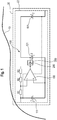
- the present invention relates to an accumulator arrangement according to the preamble of claim 1, an electric drive with an electric machine connected to such an accumulator arrangement according to claim 9 and a motor vehicle 10 having such an electric drive.
- So-called voltage balancing circuits have been developed in order to make the voltage that can be delivered thereby as uniform as possible in an accumulator arrangement that contains different accumulator units and thereby achieve the best possible performance.
- a circuit of this type is described which compares the battery units to be symmetrized - which can also include several battery cells - by means of a voltage follower circuit on a voltage divider (reference) connected in parallel.
- this circuit was made according to US 2014/0035360 A1 interconnected in such a way that it can also be scaled as required.
- the present invention is based on the object of specifying an accumulator arrangement in which the aforementioned problem of impaired energy efficiency is eliminated.
- a first embodiment of a storage battery arrangement 100 is shown.
- a first accumulator unit 111 and a second accumulator unit 121 as well as a third accumulator unit 131 are connected in series.
- a differential amplifier 150 designed as an operational amplifier is provided, the output of which is coupled to a second pole of the second accumulator unit 121, here the positive pole.
- a non-inverting input of the differential amplifier 150 is connected to the positive pole of the first accumulator unit 111.
- An inverting input of the differential amplifier 150 is connected to the first pole of the first accumulator unit 111, here the negative pole, via a first resistor R1.
- the non-inverting input of the differential amplifier 150 is connected to the output via a second resistor R2 and a resistor R0 of the differential amplifier 150 and connected to the positive pole of the second accumulator unit 121.
- the differential amplifier 150 operates as a voltage amplifier with a gain factor of 2 due to its wiring.
- a coupling element 200 which is designed here as a "simple" diode 210, is connected between the output of the differential amplifier 150 - behind the connection point of the feedback loop - and the second pole of the second accumulator unit 121.
- This diode 210 prevents the second accumulator unit 121 for balancing the entire accumulator arrangement 100 from being discharged, while on the other hand it enables the second accumulator unit 121 to be charged for balancing purposes.
- a higher energy efficiency is achieved as a result, since no energy contained in the second accumulator unit 121 is converted into heat by discharging and is thus lost.
- the wiring of the differential amplifier 150 is made in such a way that the gate voltage of the diode characteristic and the flow resistance of the diode are approximately to completely compensated.
- the design of R0 in the circuits can be done in such a way that the differential amplifier provides a voltage at the output which is composed of the voltage of the accumulator unit in the charged state and the lock voltage of the diode used.
- the flow resistance of the diode can also be approximately compensated by R1 and R2.
- the first pole of the first accumulator unit 111 and the second pole of the third accumulator unit 131 serve as a voltage supply or reference for the differential amplifier 150.
- the first accumulator unit 121 can be formed from a single accumulator cell or from a plurality of accumulator cells connected in series.
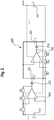
- a string of series-connected accumulator units 111, 121, 131, 141 and / or groups of accumulators can be completely balanced if all the accumulator units of the string are connected as in the cascaded arrangement of Fig. 2 which is a second embodiment of the accumulator assembly 200 according to the invention.
- the explanations made in connection with the first embodiment also apply to this second embodiment and to the further embodiments, unless stated otherwise or unless this is not prohibited by itself.
- Fig. 3 shows a third embodiment of the accumulator arrangement 300 according to the invention, which is essentially complementary to the first embodiment.
- a first accumulator unit 111 and a second accumulator unit 121 are connected in series.
- the output of the differential amplifier 150 is connected to the second, negative pole of the second accumulator unit 121.
- the non-inverting input of the differential amplifier 150 is connected to the negative pole of the first accumulator unit 111, and the inverting input of the differential amplifier 150 is coupled to a first, positive pole of the first accumulator unit 111 via a first resistor R1.
- the inverting input of the differential amplifier 150 is coupled to the output of the differential amplifier 150 or to the negative pole of the second accumulator unit 121 via a second resistor R2 and a resistor R0.
- a diode 210 is connected between the output of the differential amplifier 150 and the second connection of the second accumulator unit 121. This enables the diode 210 to perform the same function as in the first embodiment.
- the differential amplifier 150 has a gain of -1 due to its wiring.
- the value of the first resistor R1 and the value of the second resistor R2 are identical in this embodiment.
- the differential amplifier 150 and its wiring ensure that the same potential is applied to the connections of the first accumulator unit 111 and the second accumulator unit 121.
- the first accumulator unit 111 and the second accumulator unit 121 are symmetrical with respect to one another.
- the balancing ensures that a higher proportion of the charge in the accumulator units 111, 121 is available for power consumers connected to them.
- the fourth embodiment of the accumulator arrangement 400 shown here is possible to arrange a plurality of differential amplifiers 150 in cascade in order to symmetrize more than just two or three accumulator units 111, 121, 131.
- a transistor 220 is shown by way of example in this fourth embodiment. With appropriate wiring and control by a control device 230, shown only schematically, of this transistor 220, the transistor 220 can perform the same function as the diode 210 (or any other accumulator unit, to which it is assigned) offers. By means of suitable control, the extent to which the battery unit in question is discharged can be limited to a desired maximum limit. It goes without saying that such transistors 220 can also be used in place of the illustrated diodes 210 in all other embodiments.
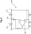
- a differential amplifier 150 is wired in such a way that it forms a voltage follower circuit for voltage balancing.
- a first accumulator unit 111 and a second accumulator unit 121 are connected in series.
- the output of the differential amplifier 150 is connected via a diode 210 to a point between the first, negative pole of the first accumulator unit 111 and the second, positive pole of the second accumulator unit 121.
- the non-inverting input of the differential amplifier 150 is connected to the negative pole of the second accumulator unit 121 via a first resistor R1 and a resistor R0 and is coupled to the positive pole of the first accumulator unit 111 via a second resistor R2.
- the inverting input of the differential amplifier 150 is connected to the output of the differential amplifier 150 and thus also connected to the point between the first, negative pole of the first accumulator unit 111 and the second, positive pole of the second accumulator unit 121.
- This voltage follower circuit has a gain of 1 due to its wiring. In this case, the voltages of the parallel voltage divider are impressed on the cells.
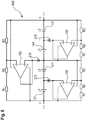
- Fig. 6 which represents an embodiment that does not fall under the present invention
- several differential amplifiers 150 can be provided in a battery arrangement 600 according to the invention analogously to the second and fourth embodiment and used in a cascade arrangement for several battery units 111, 121, 131, 141 .
- a diode can also be connected behind the negative feedback of the differential amplifier or operational amplifier and the gain can be matched to the diode characteristic using an additional resistor R0.
- This basic circuit can - based on the US 2014/0035360 A1 - in the in Fig.
Landscapes
- Engineering & Computer Science (AREA)
- Power Engineering (AREA)
- Manufacturing & Machinery (AREA)
- General Chemical & Material Sciences (AREA)
- Electrochemistry (AREA)
- Chemical Kinetics & Catalysis (AREA)
- Chemical & Material Sciences (AREA)
- Mechanical Engineering (AREA)
- Transportation (AREA)
- Sustainable Energy (AREA)
- Sustainable Development (AREA)
- Life Sciences & Earth Sciences (AREA)
- Microelectronics & Electronic Packaging (AREA)
- Charge And Discharge Circuits For Batteries Or The Like (AREA)
- Amplifiers (AREA)
Description
- Die vorliegende Erfindung betrifft eine Akkumulatoranordnung gemäß dem Oberbegriff des Anspruchs 1, einen elektrischen Antrieb mit einer an eine solche Akkumulatoranordnung angeschlossenen elektrischen Maschine gemäß Anspruch 9 sowie ein Kraftfahrzeug 10, welches einen derartigen elektrischen Antrieb aufweist.
- Um bei einer Akkumulatoranordnung, die verschiedene Akkumulatoreinheiten enthält, die hierdurch lieferbare Spannung möglichst gleichmäßig zu machen und dadurch eine möglichst gute Leistungsfähigkeit zu erzielen, wurden sogenannte Spannungssymmetrierschaltungen (häufig auch als battery cell balancing circuits bezeichnet) entwickelt. So ist beispielsweise in der
US 2005/0269989 A1 eine derartige Schaltung beschrieben, welche die zu symmetrierenden Akkumulatoreinheiten - die auch mehrere Akkumulatorzellen umfassen können - durch eine Spannungsfolgerschaltung an einem parallel geschalteten Spannungsteiler (Referenz) abgleicht. Ferner wurde diese Schaltung gemäßUS 2014/0035360 A1 so verschaltet, dass diese auch beliebig skalierbar wurde. - In der
DE 10 2016 207 555 A1 ist eine Akkumulatoranordnung gemäß dem Oberbegriff des Anspruchs 1 beschrieben, bei der als Referenz eine andere in Reihe verschaltete Zellspannung genutzt wird. Der Faktor der Zellspannung der "Vorgängerzelle" ist dabei -1, und der Faktor des "Nachfolgers" ist 2. Hierbei wird auf die zu symmetrierenden Akkumulatoreinheiten durch Laden und Entladen eingewirkt. Im Fall des Entladens wird Energie aus den Zellen bzw. Akkumulatoreinheiten in Wärme umgewandelt und damit gleichsam vernichtet. Dies beeinträchtigt die Energieeffizienz. Weitere Dokumente zum Stand der Technik sindUS 5 773 159 A undUS 2006/194102 A1 . - Der vorliegenden Erfindung liegt die Aufgabe zugrunde, eine Ackumulatoranordnung anzugeben, bei der das vorgenannte Problem der beeinträchtigten Energieeffizienz beseitigt ist.
- Diese Aufgabe wird gelöst mit einer Akkumulatoranordnung gemäß Anspruch 1. Vorteilhafte Weiterbildungen der Erfindung sind Gegenstand der abhängigen Ansprüche.
- Einige vorteilhafte Ausführungsformen der Erfindung werden nachfolgend anhand der Figuren beispielhaft erläutert.
- Es zeigen:
-
Fig. 1 eine erste Ausführungsform der erfindungsgemäßen Akkumulatoranordnung mit einem Differenzverstärker, der als Spannungssymmetrierer per nicht-invertierendem Verstärker beschaltet ist; -
Fig. 2 eine zweite Ausführungsform der erfindungsgemäßen Ackumulatoranordnung mit mehreren in Serie geschalteten Akkumulatoreinheiten und kaskadiert geschalteten Differenzverstärkern, die jeweils als Spannungssymmetrierer per nicht-invertierendem Verstärker beschaltet sind; -
Fig. 3 eine dritte Ausführungsform der erfindungsgemäßen Akkumulatoranordnung mit einem Differenzverstärker, der als Spannungssymmetrierer per invertierendem Verstärker beschaltet ist; -
Fig. 4 eine vierte Ausführungsform der erfindungsgemäßen Akkumulatoranordnung mit mehreren in Serie geschalteten Akkumulatoreinheiten und kaskadiert geschalteten Differenzverstärkern, die jeweils als Spannungssymmetrierer per invertierendem Verstärker beschaltet sind; -
Fig. 5 ein Beispiel, das nicht unter die vorliegende Erfindung fällt, mit einem Differenzverstärker, der als Spannungssymmetrierer per Spannungsfolgerschaltung beschaltet ist; und -
Fig. 6 ein Beispiel, das nicht unter die vorliegende Erfindung fällt, mit mehreren in Serie geschalteten Akkumulatoreinheiten und kaskadiert geschalteten Differenzverstärkern, die jeweils als Spannungssymmetrierer per Spannungsfolgerschaltung beschaltet sind. - In
Fig. 1 ist eine erste Ausführungsform einer erfindungsgemäßen Akkumulatoranordnung 100 dargestellt. Eine erste Akkumulatoreinheit 111 und eine zweite Akkumulatoreinheit 121 sowie eine dritte Akkumulatoreinheit 131 sind in Serie geschaltet. Es ist ein als Operationsverstärker ausgebildeter Differenzverstärker 150 vorgesehen, dessen Ausgang mit einem zweiten Pol der zweiten Akkumulatoreinheit 121, hier dem positiven Pol, gekoppelt ist. Ein nicht-invertierender Eingang des Differenzverstärkers 150 ist mit dem positiven Pol der ersten Akkumulatoreinheit 111 verbunden. Ein invertierender Eingang des Differenzverstärkers 150 ist über einen ersten Widerstand R1 mit dem ersten Pol der ersten Akkumulatoreinheit 111, hier dem negativen Pol, verbunden. Der nicht-invertierende Eingang des Differenzverstärkers 150 ist über einen zweiten Widerstand R2 sowie einen Widerstand R0 mit dem Ausgang des Differenzverstärkers 150 und mit dem positiven Pol der zweiten Akkumulatoreinheit 121 verbunden. Bei dieser ersten Ausführungsform arbeitet der Differenzverstärker 150 aufgrund seiner Beschaltung als Spannungsverstärker mit dem Verstärkungsfaktor 2. - Erfindungsgemäß ist zwischen den Ausgang des Differenzverstärkers 150 - hinter der Verbindungsstelle der Rückkopplungsschleife - und den zweiten Pol der zweiten Akkumulatoreinheit 121 ein Koppelglied 200, das hier als "einfache" Diode 210 ausgebildet ist, geschaltet. Diese Diode 210 verhindert, dass die zweite Akkumulatoreinheit 121 für die Symmetrierung der gesamten Akkumulatoranordnung 100 entladen wird, während sie andererseits ermöglicht, dass die zweite Akkumulatoreinheit 121 für die Zwecke des Symmetrierung geladen wird. Dadurch wird eine höhere Energieeffizienz erreicht, da keine in der zweiten Ackumulatoreinheit 121 enthaltene Energie durch Entladen in Wärme umgewandelt wird und damit verloren geht. Es bleibt zu erwähnen, dass auch eine andere Diode, wie beispielsweise eine Zener-Diode, statt der vorgenannten "einfachen" Diode 210 verwendet werden kann. Hierbei ist zu beachten, dass die Beschaltung des Differenzverstärkers 150 so vorgenommen ist, dass die Schleusenspannung der Diodenkennlinie und der Flusswiderstand der Diode annähernd bis vollständig kompensiert wird. Die Auslegung von R0 in den Schaltungen kann so erfolgen, dass der Differenzverstärker am Ausgang eine Spannung bereitstellt, welche sich aus der Spannung der Akkumulatoreinheit im geladenen Zustand und der Schleusenspannung der verwendeten Diode zusammensetzt. Der Flusswiderstand der Diode kann ebenfalls durch R1 und R2 annähernd kompensiert werden.
- Wie in
Fig. 1 dargestellt, dient der erste Pol der ersten Akkumulatoreinheit 111 sowie der zweite Pol der dritten Akkumulatoreinheit 131 als Spannungsversorgung bzw. Referenz für den Differenzverstärker 150. - Es versteht sich, dass bei dieser Ausführungsform die erste Ackumulatoreinheit 121 aus einer einzigen Akkumulatorzelle oder einer Mehrzahl von in Serie hintereinander geschalteten Akkumulatorzellen gebildet sein kann.
- Ferner kann sich ein Strang von in Serie geschalteten Akkumulatoreinheiten 111, 121, 131, 141 und/oder Akkumulatorgruppen vollständig symmetrieren, wenn alle Akkumulatoreinheiten des Stranges so geschaltet sind, wie es in der kaskadierten Anordnung von
Fig. 2 dargestellt ist, die eine zweite Ausführungsform der erfindungsgemäßen Ackumulatoranordnung 200 darstellt. Die im Zusammenhang mit der ersten Ausführungsform vorgenommenen Erläuterungen gelten auch für diese zweite Ausführungsform sowie für die weiteren Ausführungsformen, sofern nichts Gegenteiliges ausgeführt wird oder sofern sich dieses nicht von selbst verbietet. -
Fig. 3 zeigt eine dritte Ausführungsform der erfindungsgemäßen Akkumulatoranordnung 300, die im Wesentlichen komplementär zur ersten Ausführungsform ist. Eine erste Akkumulatoreinheit 111 und eine zweite Akkumulatoreinheit 121 sind in Serie geschaltet. Der Ausgang des Differenzverstärkers 150 ist an den zweiten, negativen Pol der zweiten Akkumulatoreinheit 121 angeschlossen. Der nicht-invertierende Eingang des Differenzverstärkers 150 ist an den negativen Pol der ersten Akkumulatoreinheit 111 angeschlossen, und der invertierende Eingang des Differenzverstärkers 150 ist über einen ersten Widerstand R1 mit einem ersten, positiven Pol der ersten Akkumulatoreinheit 111 gekoppelt. Außerdem ist der invertierende Eingang des Differenzverstärkers 150 über einen zweiten Widerstand R2 sowie einen Widerstand R0 mit dem Ausgang des Differenzverstärkers 150 bzw. mit dem negativen Pol der zweiten Akkumulatoreinheit 121 gekoppelt. - Mit umgekehrter Polung wie bei der ersten Ausführungsform ist hier eine Diode 210 zwischen den Ausgang des Differenzverstärkers 150 und den zweiten Anschluss der zweiten Akkumulatoreinheit 121 geschaltet. Dadurch kann die Diode 210 die gleiche Funktion wie bei der ersten Ausführungsform erfüllen.
- Bei dieser dritten Ausführungsform weist der Differenzverstärker 150 aufgrund seiner Beschaltung eine Verstärkung von -1 auf. Der Wert des ersten Widerstands R1 und der Wert des zweiten Widerstands R2 sind bei dieser Ausführungsform identisch.
- Durch den Differenzverstärker 150 und dessen Beschaltung wird erreicht, dass an den Anschlüssen der ersten Akkumulatoreinheit 111 und der zweiten Akkumulatoreinheit 121 das gleiche Potenzial anliegt. Folglich sind die erste Akkumulatoreinheit 111 und die zweite Akkumulatoreinheit 121 zueinander symmetriert. Wie bereits erwähnt, wird durch die Symmetrierung erreicht, dass ein höherer Anteil der Ladung in den Akkumulatoreinheiten 111, 121 für daran angeschlossene Stromverbraucher verfügbar ist.
- Ähnlich wie bei der in
Fig. 2 gezeigten zweiten Ausführungsform ist es auch bei einer inFig. 4 dargestellten vierten Ausführungsform der Akkumulatoranordnung 400 möglich, mehrere Differenzverstärker 150 kaskadiert anzuordnen, um mehr als nur zwei bzw. drei Akkumulatoreinheiten 111, 121, 131 zu symmetrieren. Als Alternative zur Verwendung der bei den ersten drei Ausführungsformen verwendeten Diode 210 ist bei dieser vierten Ausführungsform beispielhaft ein Transistor 220 dargestellt. Bei entsprechender Beschaltung und Ansteuerung durch eine lediglich schematisch dargestellte Ansteuereinrichtung 230 dieses Transistors 220 kann der Transistor 220 die gleiche Funktion ausführen wie die Diode 210. Darüber hinaus ist es möglich, den Transistor 220 so anzusteuern, dass er eine Möglichkeit der Entladung der zweiten Akkumulatoreinheit 121 (bzw. jedweder anderen Akkumulatoreinheit, der er zugeordnet ist) bietet. Durch geeignete Steuerung kann dabei das Maß der Entladung der betreffenden Akkumulatoreinheit auf eine gewünschte Höchstgrenze beschränkt werden. Es versteht sich, dass auch bei allen übrigen Ausführungsformen derartige Transistoren 220 anstelle der dargestellten Dioden 210 eingesetzt werden können. - In
Fig. 5 ist ein Ausführungsbeispiel, welches nicht unter die vorliegende Erfindung fällt, dargestellt. Ein Differenzverstärker 150 ist dabei so beschaltet, dass er eine Spannungsfolgerschaltung für die Spannungssymmetrierung bildet. Wiederum sind eine erste Akkumulatoreinheit 111 und eine zweite Akkumulatoreinheit 121 in Serie geschaltet. Der Ausgang des Differenzverstärkers 150 ist über eine Diode 210 mit einer Stelle zwischen dem ersten, negativen Pol der ersten Akkumulatoreinheit 111 und dem zweiten, positiven Pol der zweiten Akkumulatoreinheit 121 verbunden. Der nicht-invertierende Eingang des Differenzverstärkers 150 ist über einen ersten Widerstand R1 sowie einen Widerstand R0 an den negativen Pol der zweiten Akkumulatoreinheit 121 angeschlossen sowie über einen zweiten Widerstand R2 an den positiven Pol der ersten Akkumulatoreinheit 111 angekoppelt. Der invertierende Eingang des Differenzverstärkers 150 ist mit dem Ausgang des Differenzverstärkers 150 verbunden und damit ebenfalls mit der Stelle zwischen dem ersten, negativen Pol der ersten Akkumulatoreinheit 111 und dem zweiten, positiven Pol der zweiten Akkumulatoreinheit 121 verbunden. Diese Spannungsfolgerschaltung weist aufgrund ihrer Beschaltung eine Verstärkung von 1 auf. In diesem Fall werden die Spannungen des parallelen Spannungsteilers den Zellen aufgeprägt. - Gemäß Darstellung in
Fig. 6 , welche ein Ausführungsbeispiel darstellt, das nicht unter die vorliegende Erfindung fällt, können analog zu der zweiten und der vierten Ausführungsform mehrere Differenzverstärker 150 in einer erfindungsgemäßen Akkumulatoranordnung 600 vorgesehen und in einer Kaskaden-Anordnung für mehrere Akkumulatoreinheiten 111, 121, 131, 141 eingesetzt werden. In der aus der eingangs genanntenUS 2005/0269989 A1 bekannten Symmetrierschaltung kann ebenfalls eine Diode hinter der Gegenkopplung des Differenzverstärkers bzw. Operationsverstärkers geschalten und eine Anpassung der Verstärkung an die Diodenkennlinie über einen zusätzlichen Widerstand R0 vorgenommen werden. Diese Grundschaltung kann - in Anlehnung an dieUS 2014/0035360 A1 - in der inFig. 6 dargestellten Weise skaliert werden, so dass über Spannungsteiler im unteren Bereich durch Spannungsfolgerschaltungen jeweils Blöcke von zwei Zellen symmetriert werden. Zusätzlich symmetriert ein zweiter Spannungsteiler im oberen Bereich ebenfalls über eine Spannungsfolgerschaltung übergreifend die zwei Zellblöcke. - Es ist festzuhalten, dass die unter Bezug auf einzelne Ausführungsformen bzw. Varianten beschriebenen Merkmale der Erfindung, wie beispielsweise Art und Ausgestaltung des Koppelglieds sowie der einzelnen Widerstände sowie deren räumliche Anordnung, auch bei anderen Ausführungsformen vorhanden sein können, außer wenn es anders angegeben ist oder sich aus technischen Gründen von selbst verbietet.
Claims (8)
- Akkumulatoranordnung (100; 200; 300; 400; 500; 600), umfassend:eine erste Akkumulatoreinheit (111) mit einem ersten Anschluss und einem zweiten Anschluss;eine in Serie zur ersten Akkumulatoreinheit (111) geschaltete zweite Akkumulatoreinheit (121) mit einem ersten Anschluss und einem zweiten Anschluss; undeinen Differenzverstärker (150) mit einem invertierenden Eingang, einem nicht-invertierenden Eingang und einem Ausgang, an dem eine verstärkte Differenz zwischen dem Signal am invertierenden Eingang und dem Signal am nicht-invertierenden Eingang anliegt; wobei- der nicht-invertierende Eingang des Differenzverstärkers (150) mit dem zweiten Anschluss der ersten Akkumulatoreinheit (111) und dem ersten Anschluss der zweiten Akkumulatoreinheit (121) verbunden ist,- der invertierende Eingang des Differenzverstärkers (150) mit dem ersten Anschluss der ersten Akkumulatoreinheit (111) und mit dem zweiten Anschluss der zweiten Akkumulatoreinheit (121) gekoppelt ist, sowie- der Ausgang des Differenzverstärkers (150) an den zweiten Anschluss der zweiten Akkumulatoreinheit (121) angeschlossen ist;dadurch gekennzeichnet, dass zwischen den Ausgang des Differenzverstärkers (150) und den zweiten Anschluss der zweiten Akkumulatoreinheit (121) ein Koppelglied (200) mit zwei Lastanschlüssen geschaltet ist, welches das Aufladen der zweiten Akkumulatoreinheit (121) über das Koppelglied (200) ermöglicht, jedoch höchstens ein geringfügiges Entladen der zweiten Akkumulatoreinheit (121) in Richtung zum Ausgang des Differenzverstärkers (150) zulässt,wobei der erste Pol der ersten Akkumulatoreinheit (111) sowie der zweite Pol einer dritten in Serie geschalteten Akkumulatoreinheit (131) als Spannungsversorgung oder Referenz für den Differenzverstärker (150) dienen.
- Akkumulatoranordnung (100; 200; 300; 400; 500; 600) nach Anspruch 1,
dadurch gekennzeichnet, dass das Koppelglied (200) eine Diode (210) ist. - Akkumulatoranordnung (300) nach Anspruch 1,
dadurch gekennzeichnet, dass das Koppelglied (200) ein Transistor (220) ist, der so in einem Bereich steuerbar ist, dass die zweite Ackumulatoreinheit in Richtung zum Ausgang des Differenzverstärkers (150) hin überhaupt nicht oder bis zu einem bestimmten geringfügigen Maß entladbar ist. - Akkumulatoranordnung (300; 400) nach einem der Ansprüche 1 bis 3,
dadurch gekennzeichnet, dass der Differenzverstärker (150) so beschaltet ist, dass er als Spannungssymmetrierer per invertierendem Verstärker ausgestaltet ist. - Akkumulatoranordnung (200; 400; 600) nach einem der vorhergehenden Ansprüche,
dadurch gekennzeichnet, dass eine Mehrzahl von Differenzverstärkern (150) vorgesehen ist, die kaskadiert geschaltet sind. - Akkumulatoranordnung (100; 200; 300; 400; 500; 600) nach einem der vorhergehenden Ansprüche,
dadurch gekennzeichnet, dass die dritte Akkumulatoreinheit (131) mit einem ersten Anschluss und einem zweiten Anschluss vorgesehen ist, wobei deren zweiter Anschluss sowie der Versorgungsanschluss des Differenzverstärkers (150) an einen zweiten Pol der Spannungsversorgung angeschlossen ist, während der erste Anschluss der ersten Akkumulatoreinheit (121) sowie der Versorgungsanschluss des Differenzverstärkers (150) an einen ersten Pol der Spannungsversorgung angeschlossen ist. - Elektrischer Antrieb (20), mit einer elektrischen Maschine (22), die an der Akkumulatoranordnung (100; 200; 300; 400; 500; 600) gemäß einem der Ansprüche 1 bis 8 angeschlossen ist.
- Kraftfahrzeug (10), umfassend einen elektrischen Antrieb (20) gemäß Anspruch 7.
Applications Claiming Priority (2)
| Application Number | Priority Date | Filing Date | Title |
|---|---|---|---|
| DE102017214699.0A DE102017214699A1 (de) | 2017-08-23 | 2017-08-23 | Akkumulatoranordnung mit verbesserter Symmetrierung |
| PCT/EP2018/070370 WO2019038021A1 (de) | 2017-08-23 | 2018-07-27 | Akkumulatoranordnung mit verbesserter symmetrierung |
Publications (2)
| Publication Number | Publication Date |
|---|---|
| EP3673553A1 EP3673553A1 (de) | 2020-07-01 |
| EP3673553B1 true EP3673553B1 (de) | 2021-09-01 |
Family
ID=63042036
Family Applications (1)
| Application Number | Title | Priority Date | Filing Date |
|---|---|---|---|
| EP18746691.7A Active EP3673553B1 (de) | 2017-08-23 | 2018-07-27 | Akkumulatoranordnung mit verbesserter symmetrierung |
Country Status (5)
| Country | Link |
|---|---|
| US (1) | US11764600B2 (de) |
| EP (1) | EP3673553B1 (de) |
| CN (1) | CN110800186B (de) |
| DE (1) | DE102017214699A1 (de) |
| WO (1) | WO2019038021A1 (de) |
Families Citing this family (2)
| Publication number | Priority date | Publication date | Assignee | Title |
|---|---|---|---|---|
| DE102020100646B4 (de) | 2020-01-14 | 2021-08-05 | Bayerische Motoren Werke Aktiengesellschaft | Autonomer Batterie-Zellspannungssymmetrierer |
| US12487291B2 (en) | 2021-08-23 | 2025-12-02 | Chaojiong Zhang | System for determining battery parameters |
Family Cites Families (8)
| Publication number | Priority date | Publication date | Assignee | Title |
|---|---|---|---|---|
| JPH08223907A (ja) * | 1995-02-06 | 1996-08-30 | Internatl Business Mach Corp <Ibm> | 電源装置及び電源供給方法 |
| US5773159A (en) * | 1995-07-18 | 1998-06-30 | Beard; Paul | Multicell configuration for lithium cells or the like |
| AU2003900633A0 (en) * | 2003-02-13 | 2003-02-27 | Energy Storage Systems Pty Ltd | A resistive balance for an energy storage device |
| US20050077875A1 (en) * | 2003-10-14 | 2005-04-14 | Bohley Thomas K. | Battery cell balancing circuit |
| US20050269989A1 (en) | 2004-06-05 | 2005-12-08 | Geren Michael D | Cell balancing circuit |
| DE102011002452A1 (de) | 2011-01-05 | 2012-07-05 | Sb Limotive Company Ltd. | Batterie mit autonomem Cell-Balancing |
| US20170166078A1 (en) * | 2015-12-11 | 2017-06-15 | Ford Global Technologies, Llc | Battery charge equalization system |
| DE102016207555A1 (de) | 2016-05-02 | 2017-11-02 | Bayerische Motoren Werke Aktiengesellschaft | Akkumulatoranordnung mit einer verbesserten Symmetrierung |
-
2017
- 2017-08-23 DE DE102017214699.0A patent/DE102017214699A1/de not_active Withdrawn
-
2018
- 2018-07-27 WO PCT/EP2018/070370 patent/WO2019038021A1/de not_active Ceased
- 2018-07-27 CN CN201880041861.0A patent/CN110800186B/zh active Active
- 2018-07-27 EP EP18746691.7A patent/EP3673553B1/de active Active
-
2020
- 2020-01-21 US US16/748,013 patent/US11764600B2/en active Active
Also Published As
| Publication number | Publication date |
|---|---|
| WO2019038021A1 (de) | 2019-02-28 |
| DE102017214699A1 (de) | 2019-02-28 |
| EP3673553A1 (de) | 2020-07-01 |
| CN110800186B (zh) | 2023-07-14 |
| US11764600B2 (en) | 2023-09-19 |
| CN110800186A (zh) | 2020-02-14 |
| US20200161891A1 (en) | 2020-05-21 |
Similar Documents
| Publication | Publication Date | Title |
|---|---|---|
| EP2661786B1 (de) | Batterie mit autonomen cell-balancing | |
| EP2920599B1 (de) | Prüfanordnung für einen energiespeicher | |
| DE60132414T2 (de) | Universelles Batterieladegerät und Verfahren | |
| DE202011110740U1 (de) | Batterie mit mehreren Akkumulator-Zellen | |
| EP3600949B1 (de) | Zweispannungsbatterie | |
| DE102017208030B4 (de) | Bordnetz für ein Kraftfahrzeug zur Bereitstellung einer redundanten Energieversorgung für Sicherheitsverbraucher und Kraftfahrzeug | |
| DE102009028977A1 (de) | Batteriesystem | |
| EP2601721A2 (de) | Batteriesystem sowie verfahren zur ladung einer vielzahl von in reihe geschalteten batteriezellen | |
| EP2640593B1 (de) | Autonomes batterie-balancing | |
| EP2572429A2 (de) | Batterie-balancing mit reduziertem schaltungsaufwand | |
| EP3173280B1 (de) | Batterie, fahrzeug mit einer solchen batterie und verwendung einer solchen batterie | |
| EP3673553B1 (de) | Akkumulatoranordnung mit verbesserter symmetrierung | |
| DE102010029015A1 (de) | Induktives Batterie-Balancing mit reduziertem Schaltungsaufwand | |
| DE102006022394B4 (de) | Vorrichtung zum Ladungsabgleich einer Energiequelle mit mehreren Zellen | |
| EP2859366B1 (de) | Verfahren und vorrichtung zur ermittlung des innenwiderstandes von batteriezellen einer batterie | |
| EP3092148B1 (de) | Elektrochemischer speicherverbund | |
| DE102010011916A1 (de) | Batterie zur Speicherung von elektrischer Energie | |
| DE102012201359A1 (de) | Batteriesystem, Kraftfahrzeug mit einem solchen Batteriesystem sowie ein Verfahren zum Balancieren der Batteriezellen eines Batteriesystems | |
| WO2008092756A2 (de) | Batterie mit z-dioden-spannungsbegrenzungsschaltung | |
| DE102016007000A1 (de) | Vorladung über Transformator | |
| DE102012011604A1 (de) | Verfahren zum Betrieb einer Batterie für ein Fahrzeug sowie entsprechende Batterieanordnung und Fahrzeug | |
| DE102018206822A1 (de) | Elektrische Energiespeichervorrichtung, Verfahren und System zum Betreiben einer elektrischen Energiespeichervorrichtung sowie Fahrzeug | |
| WO2014023441A1 (de) | Batterie mit einer mehrzahl von parallel geschalteten batteriesträngen und verfahren zum betreiben der batterie | |
| DE102016207555A1 (de) | Akkumulatoranordnung mit einer verbesserten Symmetrierung | |
| DE102020100646B4 (de) | Autonomer Batterie-Zellspannungssymmetrierer |
Legal Events
| Date | Code | Title | Description |
|---|---|---|---|
| STAA | Information on the status of an ep patent application or granted ep patent |
Free format text: STATUS: UNKNOWN |
|
| STAA | Information on the status of an ep patent application or granted ep patent |
Free format text: STATUS: THE INTERNATIONAL PUBLICATION HAS BEEN MADE |
|
| PUAI | Public reference made under article 153(3) epc to a published international application that has entered the european phase |
Free format text: ORIGINAL CODE: 0009012 |
|
| STAA | Information on the status of an ep patent application or granted ep patent |
Free format text: STATUS: REQUEST FOR EXAMINATION WAS MADE |
|
| 17P | Request for examination filed |
Effective date: 20200211 |
|
| AK | Designated contracting states |
Kind code of ref document: A1 Designated state(s): AL AT BE BG CH CY CZ DE DK EE ES FI FR GB GR HR HU IE IS IT LI LT LU LV MC MK MT NL NO PL PT RO RS SE SI SK SM TR |
|
| AX | Request for extension of the european patent |
Extension state: BA ME |
|
| DAV | Request for validation of the european patent (deleted) | ||
| DAX | Request for extension of the european patent (deleted) | ||
| RIC1 | Information provided on ipc code assigned before grant |
Ipc: H01M 10/44 20060101ALI20210330BHEP Ipc: H01M 10/42 20060101ALI20210330BHEP Ipc: B60L 50/60 20190101ALI20210330BHEP Ipc: H02J 7/00 20060101AFI20210330BHEP |
|
| GRAP | Despatch of communication of intention to grant a patent |
Free format text: ORIGINAL CODE: EPIDOSNIGR1 |
|
| STAA | Information on the status of an ep patent application or granted ep patent |
Free format text: STATUS: GRANT OF PATENT IS INTENDED |
|
| INTG | Intention to grant announced |
Effective date: 20210514 |
|
| GRAS | Grant fee paid |
Free format text: ORIGINAL CODE: EPIDOSNIGR3 |
|
| GRAA | (expected) grant |
Free format text: ORIGINAL CODE: 0009210 |
|
| STAA | Information on the status of an ep patent application or granted ep patent |
Free format text: STATUS: THE PATENT HAS BEEN GRANTED |
|
| AK | Designated contracting states |
Kind code of ref document: B1 Designated state(s): AL AT BE BG CH CY CZ DE DK EE ES FI FR GB GR HR HU IE IS IT LI LT LU LV MC MK MT NL NO PL PT RO RS SE SI SK SM TR |
|
| REG | Reference to a national code |
Ref country code: GB Ref legal event code: FG4D Free format text: NOT ENGLISH |
|
| REG | Reference to a national code |
Ref country code: CH Ref legal event code: EP Ref country code: AT Ref legal event code: REF Ref document number: 1427242 Country of ref document: AT Kind code of ref document: T Effective date: 20210915 |
|
| REG | Reference to a national code |
Ref country code: DE Ref legal event code: R096 Ref document number: 502018006873 Country of ref document: DE |
|
| REG | Reference to a national code |
Ref country code: IE Ref legal event code: FG4D Free format text: LANGUAGE OF EP DOCUMENT: GERMAN |
|
| REG | Reference to a national code |
Ref country code: LT Ref legal event code: MG9D |
|
| REG | Reference to a national code |
Ref country code: NL Ref legal event code: MP Effective date: 20210901 |
|
| PG25 | Lapsed in a contracting state [announced via postgrant information from national office to epo] |
Ref country code: SE Free format text: LAPSE BECAUSE OF FAILURE TO SUBMIT A TRANSLATION OF THE DESCRIPTION OR TO PAY THE FEE WITHIN THE PRESCRIBED TIME-LIMIT Effective date: 20210901 Ref country code: RS Free format text: LAPSE BECAUSE OF FAILURE TO SUBMIT A TRANSLATION OF THE DESCRIPTION OR TO PAY THE FEE WITHIN THE PRESCRIBED TIME-LIMIT Effective date: 20210901 Ref country code: HR Free format text: LAPSE BECAUSE OF FAILURE TO SUBMIT A TRANSLATION OF THE DESCRIPTION OR TO PAY THE FEE WITHIN THE PRESCRIBED TIME-LIMIT Effective date: 20210901 Ref country code: ES Free format text: LAPSE BECAUSE OF FAILURE TO SUBMIT A TRANSLATION OF THE DESCRIPTION OR TO PAY THE FEE WITHIN THE PRESCRIBED TIME-LIMIT Effective date: 20210901 Ref country code: FI Free format text: LAPSE BECAUSE OF FAILURE TO SUBMIT A TRANSLATION OF THE DESCRIPTION OR TO PAY THE FEE WITHIN THE PRESCRIBED TIME-LIMIT Effective date: 20210901 Ref country code: NO Free format text: LAPSE BECAUSE OF FAILURE TO SUBMIT A TRANSLATION OF THE DESCRIPTION OR TO PAY THE FEE WITHIN THE PRESCRIBED TIME-LIMIT Effective date: 20211201 Ref country code: LT Free format text: LAPSE BECAUSE OF FAILURE TO SUBMIT A TRANSLATION OF THE DESCRIPTION OR TO PAY THE FEE WITHIN THE PRESCRIBED TIME-LIMIT Effective date: 20210901 Ref country code: BG Free format text: LAPSE BECAUSE OF FAILURE TO SUBMIT A TRANSLATION OF THE DESCRIPTION OR TO PAY THE FEE WITHIN THE PRESCRIBED TIME-LIMIT Effective date: 20211201 |
|
| PG25 | Lapsed in a contracting state [announced via postgrant information from national office to epo] |
Ref country code: PL Free format text: LAPSE BECAUSE OF FAILURE TO SUBMIT A TRANSLATION OF THE DESCRIPTION OR TO PAY THE FEE WITHIN THE PRESCRIBED TIME-LIMIT Effective date: 20210901 Ref country code: LV Free format text: LAPSE BECAUSE OF FAILURE TO SUBMIT A TRANSLATION OF THE DESCRIPTION OR TO PAY THE FEE WITHIN THE PRESCRIBED TIME-LIMIT Effective date: 20210901 Ref country code: GR Free format text: LAPSE BECAUSE OF FAILURE TO SUBMIT A TRANSLATION OF THE DESCRIPTION OR TO PAY THE FEE WITHIN THE PRESCRIBED TIME-LIMIT Effective date: 20211202 |
|
| PG25 | Lapsed in a contracting state [announced via postgrant information from national office to epo] |
Ref country code: IS Free format text: LAPSE BECAUSE OF FAILURE TO SUBMIT A TRANSLATION OF THE DESCRIPTION OR TO PAY THE FEE WITHIN THE PRESCRIBED TIME-LIMIT Effective date: 20220101 Ref country code: SM Free format text: LAPSE BECAUSE OF FAILURE TO SUBMIT A TRANSLATION OF THE DESCRIPTION OR TO PAY THE FEE WITHIN THE PRESCRIBED TIME-LIMIT Effective date: 20210901 Ref country code: SK Free format text: LAPSE BECAUSE OF FAILURE TO SUBMIT A TRANSLATION OF THE DESCRIPTION OR TO PAY THE FEE WITHIN THE PRESCRIBED TIME-LIMIT Effective date: 20210901 Ref country code: RO Free format text: LAPSE BECAUSE OF FAILURE TO SUBMIT A TRANSLATION OF THE DESCRIPTION OR TO PAY THE FEE WITHIN THE PRESCRIBED TIME-LIMIT Effective date: 20210901 Ref country code: PT Free format text: LAPSE BECAUSE OF FAILURE TO SUBMIT A TRANSLATION OF THE DESCRIPTION OR TO PAY THE FEE WITHIN THE PRESCRIBED TIME-LIMIT Effective date: 20220103 Ref country code: NL Free format text: LAPSE BECAUSE OF FAILURE TO SUBMIT A TRANSLATION OF THE DESCRIPTION OR TO PAY THE FEE WITHIN THE PRESCRIBED TIME-LIMIT Effective date: 20210901 Ref country code: EE Free format text: LAPSE BECAUSE OF FAILURE TO SUBMIT A TRANSLATION OF THE DESCRIPTION OR TO PAY THE FEE WITHIN THE PRESCRIBED TIME-LIMIT Effective date: 20210901 Ref country code: CZ Free format text: LAPSE BECAUSE OF FAILURE TO SUBMIT A TRANSLATION OF THE DESCRIPTION OR TO PAY THE FEE WITHIN THE PRESCRIBED TIME-LIMIT Effective date: 20210901 Ref country code: AL Free format text: LAPSE BECAUSE OF FAILURE TO SUBMIT A TRANSLATION OF THE DESCRIPTION OR TO PAY THE FEE WITHIN THE PRESCRIBED TIME-LIMIT Effective date: 20210901 |
|
| REG | Reference to a national code |
Ref country code: DE Ref legal event code: R097 Ref document number: 502018006873 Country of ref document: DE |
|
| PLBE | No opposition filed within time limit |
Free format text: ORIGINAL CODE: 0009261 |
|
| STAA | Information on the status of an ep patent application or granted ep patent |
Free format text: STATUS: NO OPPOSITION FILED WITHIN TIME LIMIT |
|
| PG25 | Lapsed in a contracting state [announced via postgrant information from national office to epo] |
Ref country code: IT Free format text: LAPSE BECAUSE OF FAILURE TO SUBMIT A TRANSLATION OF THE DESCRIPTION OR TO PAY THE FEE WITHIN THE PRESCRIBED TIME-LIMIT Effective date: 20210901 Ref country code: DK Free format text: LAPSE BECAUSE OF FAILURE TO SUBMIT A TRANSLATION OF THE DESCRIPTION OR TO PAY THE FEE WITHIN THE PRESCRIBED TIME-LIMIT Effective date: 20210901 |
|
| 26N | No opposition filed |
Effective date: 20220602 |
|
| PG25 | Lapsed in a contracting state [announced via postgrant information from national office to epo] |
Ref country code: SI Free format text: LAPSE BECAUSE OF FAILURE TO SUBMIT A TRANSLATION OF THE DESCRIPTION OR TO PAY THE FEE WITHIN THE PRESCRIBED TIME-LIMIT Effective date: 20210901 |
|
| PG25 | Lapsed in a contracting state [announced via postgrant information from national office to epo] |
Ref country code: MC Free format text: LAPSE BECAUSE OF FAILURE TO SUBMIT A TRANSLATION OF THE DESCRIPTION OR TO PAY THE FEE WITHIN THE PRESCRIBED TIME-LIMIT Effective date: 20210901 |
|
| REG | Reference to a national code |
Ref country code: CH Ref legal event code: PL |
|
| GBPC | Gb: european patent ceased through non-payment of renewal fee |
Effective date: 20220727 |
|
| REG | Reference to a national code |
Ref country code: BE Ref legal event code: MM Effective date: 20220731 |
|
| PG25 | Lapsed in a contracting state [announced via postgrant information from national office to epo] |
Ref country code: LU Free format text: LAPSE BECAUSE OF NON-PAYMENT OF DUE FEES Effective date: 20220727 Ref country code: LI Free format text: LAPSE BECAUSE OF NON-PAYMENT OF DUE FEES Effective date: 20220731 Ref country code: FR Free format text: LAPSE BECAUSE OF NON-PAYMENT OF DUE FEES Effective date: 20220731 Ref country code: CH Free format text: LAPSE BECAUSE OF NON-PAYMENT OF DUE FEES Effective date: 20220731 |
|
| PG25 | Lapsed in a contracting state [announced via postgrant information from national office to epo] |
Ref country code: GB Free format text: LAPSE BECAUSE OF NON-PAYMENT OF DUE FEES Effective date: 20220727 Ref country code: BE Free format text: LAPSE BECAUSE OF NON-PAYMENT OF DUE FEES Effective date: 20220731 |
|
| P01 | Opt-out of the competence of the unified patent court (upc) registered |
Effective date: 20230503 |
|
| PG25 | Lapsed in a contracting state [announced via postgrant information from national office to epo] |
Ref country code: IE Free format text: LAPSE BECAUSE OF NON-PAYMENT OF DUE FEES Effective date: 20220727 |
|
| PG25 | Lapsed in a contracting state [announced via postgrant information from national office to epo] |
Ref country code: MK Free format text: LAPSE BECAUSE OF FAILURE TO SUBMIT A TRANSLATION OF THE DESCRIPTION OR TO PAY THE FEE WITHIN THE PRESCRIBED TIME-LIMIT Effective date: 20210901 Ref country code: CY Free format text: LAPSE BECAUSE OF FAILURE TO SUBMIT A TRANSLATION OF THE DESCRIPTION OR TO PAY THE FEE WITHIN THE PRESCRIBED TIME-LIMIT Effective date: 20210901 |
|
| PG25 | Lapsed in a contracting state [announced via postgrant information from national office to epo] |
Ref country code: HU Free format text: LAPSE BECAUSE OF FAILURE TO SUBMIT A TRANSLATION OF THE DESCRIPTION OR TO PAY THE FEE WITHIN THE PRESCRIBED TIME-LIMIT; INVALID AB INITIO Effective date: 20180727 |
|
| PG25 | Lapsed in a contracting state [announced via postgrant information from national office to epo] |
Ref country code: TR Free format text: LAPSE BECAUSE OF FAILURE TO SUBMIT A TRANSLATION OF THE DESCRIPTION OR TO PAY THE FEE WITHIN THE PRESCRIBED TIME-LIMIT Effective date: 20210901 |
|
| REG | Reference to a national code |
Ref country code: AT Ref legal event code: MM01 Ref document number: 1427242 Country of ref document: AT Kind code of ref document: T Effective date: 20230727 |
|
| PG25 | Lapsed in a contracting state [announced via postgrant information from national office to epo] |
Ref country code: MT Free format text: LAPSE BECAUSE OF FAILURE TO SUBMIT A TRANSLATION OF THE DESCRIPTION OR TO PAY THE FEE WITHIN THE PRESCRIBED TIME-LIMIT Effective date: 20210901 |
|
| PG25 | Lapsed in a contracting state [announced via postgrant information from national office to epo] |
Ref country code: AT Free format text: LAPSE BECAUSE OF NON-PAYMENT OF DUE FEES Effective date: 20230727 |
|
| PG25 | Lapsed in a contracting state [announced via postgrant information from national office to epo] |
Ref country code: AT Free format text: LAPSE BECAUSE OF NON-PAYMENT OF DUE FEES Effective date: 20230727 |
|
| PGFP | Annual fee paid to national office [announced via postgrant information from national office to epo] |
Ref country code: DE Payment date: 20250702 Year of fee payment: 8 |
|
| PGFP | Annual fee paid to national office [announced via postgrant information from national office to epo] |
Ref country code: AT Payment date: 20260410 Year of fee payment: 5 |