EP3672082A1 - Sndr improvement through optimal dac element selection - Google Patents
Sndr improvement through optimal dac element selection Download PDFInfo
- Publication number
- EP3672082A1 EP3672082A1 EP19210477.6A EP19210477A EP3672082A1 EP 3672082 A1 EP3672082 A1 EP 3672082A1 EP 19210477 A EP19210477 A EP 19210477A EP 3672082 A1 EP3672082 A1 EP 3672082A1
- Authority
- EP
- European Patent Office
- Prior art keywords
- dac
- sndr
- unit elements
- optimal
- analog
- Prior art date
- Legal status (The legal status is an assumption and is not a legal conclusion. Google has not performed a legal analysis and makes no representation as to the accuracy of the status listed.)
- Granted
Links
Images



Classifications
-
- H—ELECTRICITY
- H03—ELECTRONIC CIRCUITRY
- H03M—CODING; DECODING; CODE CONVERSION IN GENERAL
- H03M3/00—Conversion of analogue values to or from differential modulation
- H03M3/30—Delta-sigma modulation
- H03M3/458—Analogue/digital converters using delta-sigma modulation as an intermediate step
- H03M3/464—Details of the digital/analogue conversion in the feedback path
-
- H—ELECTRICITY
- H03—ELECTRONIC CIRCUITRY
- H03M—CODING; DECODING; CODE CONVERSION IN GENERAL
- H03M3/00—Conversion of analogue values to or from differential modulation
- H03M3/30—Delta-sigma modulation
- H03M3/38—Calibration
- H03M3/386—Calibration over the full range of the converter, e.g. for correcting differential non-linearity
- H03M3/388—Calibration over the full range of the converter, e.g. for correcting differential non-linearity by storing corrected or correction values in one or more digital look-up tables
-
- H—ELECTRICITY
- H03—ELECTRONIC CIRCUITRY
- H03M—CODING; DECODING; CODE CONVERSION IN GENERAL
- H03M1/00—Analogue/digital conversion; Digital/analogue conversion
- H03M1/10—Calibration or testing
- H03M1/1009—Calibration
- H03M1/1033—Calibration over the full range of the converter, e.g. for correcting differential non-linearity
- H03M1/1038—Calibration over the full range of the converter, e.g. for correcting differential non-linearity by storing corrected or correction values in one or more digital look-up tables
-
- H—ELECTRICITY
- H03—ELECTRONIC CIRCUITRY
- H03M—CODING; DECODING; CODE CONVERSION IN GENERAL
- H03M3/00—Conversion of analogue values to or from differential modulation
- H03M3/30—Delta-sigma modulation
- H03M3/322—Continuously compensating for, or preventing, undesired influence of physical parameters
- H03M3/368—Continuously compensating for, or preventing, undesired influence of physical parameters of noise other than the quantisation noise already being shaped inherently by delta-sigma modulators
-
- H—ELECTRICITY
- H03—ELECTRONIC CIRCUITRY
- H03M—CODING; DECODING; CODE CONVERSION IN GENERAL
- H03M1/00—Analogue/digital conversion; Digital/analogue conversion
- H03M1/001—Analogue/digital/analogue conversion
-
- H—ELECTRICITY
- H03—ELECTRONIC CIRCUITRY
- H03M—CODING; DECODING; CODE CONVERSION IN GENERAL
- H03M1/00—Analogue/digital conversion; Digital/analogue conversion
- H03M1/06—Continuously compensating for, or preventing, undesired influence of physical parameters
-
- H—ELECTRICITY
- H03—ELECTRONIC CIRCUITRY
- H03M—CODING; DECODING; CODE CONVERSION IN GENERAL
- H03M1/00—Analogue/digital conversion; Digital/analogue conversion
- H03M1/10—Calibration or testing
- H03M1/1009—Calibration
-
- H—ELECTRICITY
- H03—ELECTRONIC CIRCUITRY
- H03M—CODING; DECODING; CODE CONVERSION IN GENERAL
- H03M1/00—Analogue/digital conversion; Digital/analogue conversion
- H03M1/12—Analogue/digital converters
-
- H—ELECTRICITY
- H03—ELECTRONIC CIRCUITRY
- H03M—CODING; DECODING; CODE CONVERSION IN GENERAL
- H03M1/00—Analogue/digital conversion; Digital/analogue conversion
- H03M1/66—Digital/analogue converters
-
- H—ELECTRICITY
- H03—ELECTRONIC CIRCUITRY
- H03M—CODING; DECODING; CODE CONVERSION IN GENERAL
- H03M3/00—Conversion of analogue values to or from differential modulation
- H03M3/30—Delta-sigma modulation
-
- H—ELECTRICITY
- H03—ELECTRONIC CIRCUITRY
- H03M—CODING; DECODING; CODE CONVERSION IN GENERAL
- H03M3/00—Conversion of analogue values to or from differential modulation
- H03M3/30—Delta-sigma modulation
- H03M3/39—Structural details of delta-sigma modulators, e.g. incremental delta-sigma modulators
- H03M3/412—Structural details of delta-sigma modulators, e.g. incremental delta-sigma modulators characterised by the number of quantisers and their type and resolution
- H03M3/422—Structural details of delta-sigma modulators, e.g. incremental delta-sigma modulators characterised by the number of quantisers and their type and resolution having one quantiser only
- H03M3/424—Structural details of delta-sigma modulators, e.g. incremental delta-sigma modulators characterised by the number of quantisers and their type and resolution having one quantiser only the quantiser being a multiple bit one
-
- H—ELECTRICITY
- H03—ELECTRONIC CIRCUITRY
- H03M—CODING; DECODING; CODE CONVERSION IN GENERAL
- H03M3/00—Conversion of analogue values to or from differential modulation
- H03M3/30—Delta-sigma modulation
- H03M3/458—Analogue/digital converters using delta-sigma modulation as an intermediate step
Definitions
- This disclosure relates generally to data conversion, and more specifically to improving the linearity of a Sigma-Delta Analog-to-Digital Converter (ADC).
- ADC Sigma-Delta Analog-to-Digital Converter
- a Sigma-Delta ADC encodes an analog signal into a digital output signal.
- the first step in converting the analog signal with the Sigma-Delta ADC is to form a "delta" or difference between the analog input and the digital output converted back to analog form by a Digital-to-Analog Converter (DAC).
- DAC Digital-to-Analog Converter
- Embodiments described herein provide for SNDR improvement by optimizing the linearity of a DAC in a Sigma-Delta ADC.
- the linearity of the DAC is improved by optimally selecting the order in which DAC unary current sources (e.g., elements) are selected to convert the time variant digital output of the ADC.
- the DAC output (e.g., an analog output) is comprised of the sum of the individual unit element currents, which each have a random offset current in which the cumulative offset current, and therefore the linearity, are minimized through optimal element ordering.
- Another option to reduce the DAC nonlinearity is to increase the size of the DAC elements to improve the matching between the elements. This approach increases area and power consumption, which is particularly undesirable for converters in an embedded design (e.g., on a monolithic integrated circuit).
- Embodiments described herein overcome the limitations of the aforementioned approaches requiring higher oversampling ratios for a given SNR, shaping or increasing the layout area.
- a series of analog to digital conversions with a Sigma-Delta ADC and observing the SNDR with a Fourier transform (e.g., a Fast Fourier Transform)
- an optimized ordering of the elements is determined to maximize the SNDR.
- Each conversion permutes the order of the DAC elements resulting in a different SNDR.
- the optimized ordering yielding the largest SNDR is then stored in a lookup table accessible by the DAC during data conversion operations with the Sigma-Delta ADC.
- FIG. 1 shows an embodiment 10 of a system for SNDR improvement though optimal DAC element selection in accordance with an example embodiment of the present disclosure.
- a summing circuit 12 subtracts a DAC output 14 from an analog input 16 to determine a delta value 18.
- the delta value 18 is filtered by a filter 20 to determine a filtered value 22.
- the filter 20 is a low pass filter.
- the filter 20 is a band pass filter.
- a multi-bit ADC converts the filtered value 22 into a multi-bit digital output 30 of width "N.”
- the ADC 24 is a flash ADC and the digital output 30 is coded as a thermometer code.
- a 4-bit ADC 24 has a digital output of 16 bits, which are input to the DAC 32.
- the digital output 30 is converted to a 4-bit binary code and fed into a decimation filter (not shown), thus converting the system 10, (based on a Sigma-Delta modulator) into a Sigma-Delta ADC.
- the multi-bit digital output 30 is converted into a DAC output 14 output by a unit element DAC 32.
- the DAC 32 accesses a lookup table 34 over a connection 36, to define connections between the digital inputs of the DAC 32 and the respective unit elements included therein.
- the lookup table 34 holds the values that determine an optimized ordering of the DAC elements, as further discussed with reference to FIG. 3 .
- the lookup table 34 is outside of the control loop formed by the summing circuit 12, the low pass filter 20, the multi-bit ADC and the multi-bit unit element DAC 32. Accordingly, the lookup table 34 does not add control loop delay, nor affect loop stability.
- the lookup table 34 is formed with a Non-Volatile Memory, include one or more of a laser fuse, and EPROM, a One Time Programmable memory, and the like.
- each of the DACs may have an optimized ordering of their respective unary current sources. However, most of the reduction in distortion is obtained by optimizing the DAC whose output feeds the first summing circuit connected directly to the analog input 16.
- FIG. 2 is an embodiment 20 of the filter 20 of FIG. 1 , configured as an integrator.
- An amplifier 40 includes a positive input connected to a ground 42.
- the delta value 18 of FIG. 1 is connected to a negative input 48 through a resistor 44.
- the amplifier 40 generates the filtered value 22 of FIG. 1 , which is further connected to the negative input 48 through a feedback capacitor 46. Glitch energy caused by switching of the elements of the multi-bit unit element DAC 32 is fed directly into the summing circuit 12 of FIG. 1 and integrated at the negative input 48, thus undesirably contributing to system noise.
- the number of required elements is equal to 2 N * LSB, where N is the number of bits used by the DAC 32 (e.g., the width of the multi-bit digital output 30) and LSB is the Least Significant Bit of the multi-bit path.
- N is the number of bits used by the DAC 32 (e.g., the width of the multi-bit digital output 30) and LSB is the Least Significant Bit of the multi-bit path.
- any number of elements can be used, not necessarily constrained to being a multiple of two.
- the width of the example embodiment 50 of FIG. 3 is two bits, thus requiring four unary weighted elements, wherein each element represent one LSB current relative to a full scale current. Other bit widths are envisioned with the scope of this disclosure.
- the embodiment 50 includes a bias source 50 and a DAC output 52.
- a plurality of switches 54a, 54b, 54c and 54d (generally 54), are connected in series with respective unary weighted current sources 56a, 56b, 56c and 56d (generally 56).
- Each of the current sources 56 is connected to the ground 42.
- Each switch 54 and a respective current source 56 (e.g. switch 54a and current source 56a) is referred to as an "element.”
- a digital input of "0111” (e.g., three) is represented by connecting the DAC output 52 to three elements by activating three of the four switches 54, having respective current sources 56. If the next digital input is "1111" (e.g., four), then the DAC output 52 will be connected to the remaining element.
- Each of the current sources 56 includes a nominal current plus a respective random offset current, where the respective random offset current either adds to or subtracts from the nominal current. Randomizing the order of the unit elements can be accomplished by any of the randomization methods that are well known in the art such as applying a power to the memory, which has been designed to come up in a random state at power up or using a linear feedback shift register. As the digital input to the multi-bit unit element DAC 32 of FIG. 1 changes, one or more elements are connected to the DAC output 14. Each of the unary weighted elements have the same nominal current, hence there are a plurality of combinations of selecting elements to achieve the same value of the DAC output 14 in response to a change in the digital output 30.
- the embodiment 50 is a current output DAC, which is used with an embodiment 10 where the analog input 16 is represented by a current.
- the multi-bit unit element DAC 32 supplies a voltage output (e.g., a Kelvin Divider) to the summing circuit 12 and the analog input 16 is represented by a voltage.
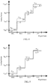
- FIG. 4 shows the nonlinear characteristics of the DAC output 14 of FIG. 1 , before optimizing the ordering of the selectable elements of the multi-bit unit element DAC 32.
- FIG. 5 shows the nonlinear characteristics of the DAC output 14 of FIG. 1 , after optimizing the ordering of the selectable elements of the multi-bit unit element DAC 32. Due to the mismatch between each of the current sources 56 of FIG. 3 , each element will have an offset, either positive or negative relative to the ideal or average value.
- the multi-bit unit element DAC 32 would use the first element, then sequentially add additional elements until all of the elements are used.
- the analog output of the DAC 32 will ideally represent a staircase with equal steps. However, due to offsets each step will be change based on the cumulative offsets of the respective elements.
- the output of the multi-bit unit element DAC 32 is shown based on a two-bit binary system with four elements.
- the digital input to the DAC 32 e.g., the digital output 30
- the DAC output 14 (or analog output) would ideally follow the equal current steps 70, 72, 74 and 76.
- step 70 is increased by an offset 80 due to the first current source 56a to yield a step 90.
- Step 72 is increased by an offset 80 from the first selected current source 56a and an offset 82 from the second selected current source 56b to yield a step 92.
- the cumulative offset is equal to 80 plus 82.
- step 94 is increased by offsets 80 and 82 and decreased by 84 (the offset from the third current source 56c) to yield a step 94.
- Step 76 is altered by offsets 80, 82, 84 and 86 (from the fourth current source 56d) to yield a step 96.
- the linearity of steps 90, 92, 94 and 96 is poor, thus causing distortion and thereby leading to low SNDR.
- FIG. 5 shows an improved linearity of the DAC 32 due to optimized ordering of elements.
- an optimized element order is chosen. Specifically, the first current source 56a is chosen for input "0000" because the offset 80 is the smallest of the four offsets.
- the fourth current source 56d is chosen so that the cumulative offset 80 and 86 largely cancel each other.
- the second current source 56b is chosen, so that the cumulative offsets 80, 86 and 82 still remain close to zero.
- the third current source 56c is chosen so that the cumulative offsets 80, 86, 82 and 84 yield a small negative offset.
- the DAC output 14 with the optimized ordering shown by 100, 102, 104 and 106 closely approximates the ideal output shown by 70, 72, 74, and 76.
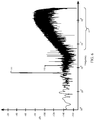
- FIG. 6 shows a Fast Fourier Transform of an output of a Sigma-Delta ADC system employing a 4-bit quantizer ADC and a 4-bit feedback DAC showing decibels relative to full scale for a range of frequencies, and using no DAC linearity correction technique such as optimized element ordering or data weighted averaging.
- the fundamental signal peak is 110 is shown in relation to a plurality of significant distortion components 112.
- Shaped noise 114 is shown to be shifted to a higher frequency band, which can be filtered with a digital low pass filter in a post processing step, however the SNDR is only 67dB with an SNR of 84dB.
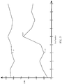
- FIG. 7 shows measured SNDR and SNR for a series of tests (numbered 1 through 10) of one ADC, where the DAC element ordering is randomly defined for each test of the system of FIG. 1 .
- the DAC elements are randomly defined upon application of power to the DAC 32.
- the randomization of the DAC elements is performed by a random number generator, (e.g., a linear feedback shift register).
- the SNR variation is only approximately 3dB due to quantization and other system noise.
- FIG. 7 shows a significant improvement in SNDR from 57dB measured from the first test run to 72dB measured from the sixth test run for the same ADC with different ordering of the DAC elements, or a 15dB improvement.
- the SNDR is measured with an external tester used for production testing of semiconductor components.
- the SNDR is measured with a wafer probe tester.
- the term "optimized ordering" as used throughout this disclosure includes an ordering of the DAC unit elements determined from a series of tests that include randomization of the unit elements that comprise the DAC that is used in the Sigma-Delta ADC of FIG. 7 .
- the tests to determine the optimized element ordering are performed during wafer probe testing.
- the tests to determine the optimized ordering of the DAC unit elements are performed during post assembly (packaging) testing.
- a full determination of all possible unit element ordering combinations of a subset of the most critical of the unit elements that comprise the DAC is determined by only considering the elements that will be used the most often (e.g.
- the optimal element ordering is defined through randomization wherein the digital output 30 is limited to a high slope region, such as zero crossing of a sinusoidal waveform. Accordingly, this limited range exceeds a slope threshold where changes to the DAC output 14 of FIG. 1 are of a greater magnitude than in low slope regions.
- FIG. 8 shows a method 130 for SNDR improvement through optimal DAC element selection.
- an order of a plurality of unit element of a DAC is randomized.
- a plurality of digital inputs, controlling the unit elements is ramped to generate analog outputs.
- a first SNDR of the DAC is measured from the analog outputs.
- a maximum SNDR is determined from the first SNDR and at least one previously measured SNDR, using the same method as used to determine the first SNDR, to determine an optimal order of the unit elements.
- the optimal order is stored in a memory to define the connections between the digital inputs and the unit elements.
- FIG. 9 shows another method 150 for SNDR improvement through optimal DAC element selection.
- an SNDR of a Sigma-Delta ADC is determined for a plurality of test runs.
- the Sigma-Delta ADC comprises the system 10 of FIG. 1 followed by a digital filter.
- Determining the SNDR at 152 comprises at 154, randomizing an order of the unit elements of a DAC within the Sigma-Delta ADC; at 156, ramping a time-variant analog input of the Sigma-Delta ADC, and at 158, measuring an SNDR of the Sigma-Delta ADC.
- a maximum SNDR is determined from each of the test runs, wherein the maximum SNDR corresponds to an optimal order of the unit elements.
- the optimal order is stored in a memory.
- a method for Signal-to-Noise and Distortion Ratio (SNDR) improvement through optimal Digital-to-Analog-Converter (DAC) element selection comprises randomizing an order of a plurality of unit elements of a DAC, wherein each of the unit elements is controlled by a respective one of a plurality of digital inputs of the DAC.
- the plurality of digital inputs are sequentially asserted over at least a subset of a full set of the digital inputs to generate a plurality of analog values of an analog output of the DAC.
- a first SNDR of the DAC is measured from the plurality of analog values.
- a maximum SNDR is determined from the first SNDR and at least one previously measured SNDR, the maximum SNDR corresponding to an optimal order of the unit elements.
- the optimal order of the unit elements of the DAC is stored in a memory to define connections between the digital inputs and the respective unit elements based on the optimal order.
- Alternative embodiments of the method for Signal-to-Noise and Distortion Ratio (SNDR) improvement through optimal Digital-to-Analog-Converter (DAC) element selection include one of the following features, or any combination thereof.
- the optimal order of the unit elements is accessed from the memory by the DAC, for subsequently converting the digital inputs to the respective analog values.
- the subset is centered within the full set.
- the subset is equal to the full set.
- the at least one previously measured SNDR comprises at least five measured SNDR.
- Randomizing the order of the unit elements comprises applying a power to the memory, wherein the memory is designed to comprise random states in response to applying the power. Randomizing the order of the unit elements comprises defining the order with a plurality of outputs of a linear feedback shift register.
- the full set of the digital inputs is determined by quantizing a sine wave.
- the full set of the digital inputs is determined by quantizing a periodic signal.
- Each of the analog values comprises a cumulative offset current formed by a summation of a respective random offset current of each unit element selected by the optimal order.
- a system for Signal-to-Noise and Distortion Ratio (SNDR) improvement through optimal Digital-to-Analog-Converter (DAC) element selection comprises a plurality of unit elements of a DAC, wherein an order of the unit elements is configured to be randomized.
- Each of a plurality of digital inputs of the DAC is configured to control a respective unit element based on the order of the unit elements.
- An analog output of the DAC is switchably connected to one or more of the unit elements based on a respective value of each of the respective digital inputs.
- a memory is configured to store the optimal order of the unit elements of the DAC to define connections between the digital inputs and the respective unit elements, wherein the optimal order is determined from an optimal test run of a plurality of test runs, each of the test runs determine a respective SNDR, and the optimal test run comprises a maximum SNDR.
- a tester is configured to determine the respective SNDR of each of the test runs by sequentially asserting the plurality of digital inputs over at least a subset of a full set of the digital inputs to generate a plurality of analog values of the analog output, and measuring the SNDR of the DAC from the plurality of analog values.
- Each of the unit elements comprise a switchable current source comprising a nominal current having a respective random offset current.
- the analog output comprises a cumulative offset current formed by a summation of a respective random offset current of each unit element selected by the optimal order.
- a Sigma-Delta Analog-to-Digital Converter comprises an ADC configured to quantize a filtered sum of the analog output of the DAC subtracted from a time-variant analog input of the Sigma-Delta ADC.
- a method for Signal-to-Noise and Distortion Ratio (SNDR) improvement through optimal Digital-to-Analog-Converter (DAC) element selection comprises determining an SNDR of a Sigma-Delta Analog-to-Digital Converter (ADC) for a plurality of test runs, wherein each test run comprises: randomizing an order of a plurality of unit elements of a DAC, the Sigma-Delta ADC comprising an ADC configured to quantize a filtered sum of an output of the DAC subtracted from a time-variant analog input of the Sigma-Delta ADC, asserting the time-variant analog input over at least a subset of a full range of the analog signal, and measuring an SNDR of the Sigma-Delta ADC.
- a maximum SNDR is determined from a respective SNDR of each of the test runs, wherein the maximum SNDR corresponds to an optimal order of the unit elements.
- the optimal order of the unit elements is stored in a memory
- Alternative embodiments of the method for Signal-to-Noise and Distortion Ratio (SNDR) improvement through optimal Digital-to-Analog-Converter (DAC) element selection include one of the following features, or any combination thereof.
- the optimal order of the unit elements is accessed from the memory by the DAC, for subsequently generating a plurality of analog values of the output of the DAC. Randomizing the order of the unit elements comprises applying a power to the memory, wherein the memory is designed to comprise random states in response to applying the power. Randomizing the order of the unit elements comprises defining the order with a plurality of outputs of a linear feedback shift register.
- the time-variant analog input is a sine wave.
- a method for Signal-to-Noise and Distortion Ratio (SNDR) improvement through optimal Digital-to-Analog-Converter (DAC) element selection includes randomizing an order of a plurality of unit elements of a DAC, wherein each of the unit elements is controlled by a respective one of a plurality of digital inputs of the DAC.
- the plurality of digital inputs is sequentially asserted over at least a subset of a full set of the digital inputs to generate a plurality of analog values of an output of the DAC.
- a first SNDR of the DAC is measured from the plurality of analog values.
- a maximum SNDR, corresponding to an optimal order, is determined from the first SNDR and at least one previously measured SNDR.
- the optimal order of the unit elements of the DAC is stored in a memory to define connections between the digital inputs and the respective unit elements based on the optimal order.
Landscapes
- Engineering & Computer Science (AREA)
- Theoretical Computer Science (AREA)
- Physics & Mathematics (AREA)
- Nonlinear Science (AREA)
- Analogue/Digital Conversion (AREA)
- Compression, Expansion, Code Conversion, And Decoders (AREA)
Abstract
Description
- This disclosure relates generally to data conversion, and more specifically to improving the linearity of a Sigma-Delta Analog-to-Digital Converter (ADC).
- A Sigma-Delta ADC encodes an analog signal into a digital output signal. The first step in converting the analog signal with the Sigma-Delta ADC is to form a "delta" or difference between the analog input and the digital output converted back to analog form by a Digital-to-Analog Converter (DAC). This feedback of the digital output through the DAC introduces a significant source of nonlinearity in the converter system, which limits the overall system performance.
- The present invention is illustrated by way of example and is not limited by the accompanying figures, in which like references indicate similar elements. Elements in the figures are illustrated for simplicity and clarity and have not necessarily been drawn to scale.
-
FIG. 1 is a schematic view of a system for Signal-to-Noise plus Distortion Ratio (SNDR) improvement through optimal DAC element selection in accordance with an example embodiment of the present disclosure. -
FIG. 2 is a schematic view of an embodiment of the filter ofFIG. 1 . -
FIG. 3 is a schematic view of an embodiment of the current-output unit element DAC ofFIG. 1 . -
FIG. 4 is a graphical view of the output of the DAC ofFIG. 1 without optimal DAC element selection. -
FIG. 5 is a graphical view of the output of the DAC ofFIG. 1 with optimal DAC element selection in accordance with an example embodiment of the present disclosure. -
FIG. 6 is a graphical view of a Fast Fourier Transform (FFT) of an output of a Sigma-Delta ADC employing a 4-bit quantizer ADC and a 4-bit feedback DAC -
FIG. 7 is a graphical view of SNDR and Signal-to-Noise Ratio (SNR) for a series of test characterization runs of the system ofFIG. 1 . -
FIG. 8 is a flowchart representation of a method for SNDR improvement through optimal DAC element selection in accordance with an example embodiment of the present disclosure. -
FIG. 9 is a flowchart representation of a method for SNDR improvement through optimal DAC element selection in accordance with an example embodiment of the present disclosure. - Embodiments described herein provide for SNDR improvement by optimizing the linearity of a DAC in a Sigma-Delta ADC. Specifically, the linearity of the DAC is improved by optimally selecting the order in which DAC unary current sources (e.g., elements) are selected to convert the time variant digital output of the ADC. The DAC output (e.g., an analog output) is comprised of the sum of the individual unit element currents, which each have a random offset current in which the cumulative offset current, and therefore the linearity, are minimized through optimal element ordering.
- The distortion due to nonlinearity in a Sigma-Delta ADC, (either continuous or discrete), is dominated by how well the feedback DAC elements match each other. Solutions to this include using a single bit feedback DAC, which implies linearity because only two element states are possible. One problem with using a single bit feedback DAC is that to obtain the same dynamic range as a multi-bit DAC, a higher oversampling ratio is required. Consequently, a higher clock rate is required, which increases power consumption.
- Another approach to reducing the nonlinearity of a Sigma-Delta ADC is to compensate for the element mismatch in the DAC with a mismatch shaping algorithm. This approach shapes the error from the DAC nonlinearity, due to the element mismatch, out of the signal band. However, this approach increases the in-band noise floor, and also adds delay to the ADC feedback loop, thus degrading loop stability. In discrete time Sigma-Delta conversion this is not as problematic, but in continuous time Sigma-Delta conversion special attention must be paid to the glitch energy that occurs with implementing shaped randomization of the DAC element choices. Shaping increases glitch energy due to the switching of the DAC elements. This glitch energy occurs at the summing junction of the integrator as the analog input and the DAC feedback are integrated. Consequently, the integration of this glitch energy can significantly degrade the conversion performance.
- Another option to reduce the DAC nonlinearity is to increase the size of the DAC elements to improve the matching between the elements. This approach increases area and power consumption, which is particularly undesirable for converters in an embedded design (e.g., on a monolithic integrated circuit).
- Embodiments described herein overcome the limitations of the aforementioned approaches requiring higher oversampling ratios for a given SNR, shaping or increasing the layout area. By executing a series of analog to digital conversions with a Sigma-Delta ADC and observing the SNDR with a Fourier transform (e.g., a Fast Fourier Transform), an optimized ordering of the elements is determined to maximize the SNDR. Each conversion permutes the order of the DAC elements resulting in a different SNDR. The optimized ordering yielding the largest SNDR, is then stored in a lookup table accessible by the DAC during data conversion operations with the Sigma-Delta ADC.
- While various embodiments of this disclosure are directed towards improving SNDR of a Sigma-Delta ADC by optimizing element ordering of a feedback DAC within the converter, similar SNDR advantages are realized by applying the teaching of this disclosure to a standalone unit element DAC. Similarly in other embodiments, SNDR improvement of a unit element DAC is advantageous in systems comprising the unit element DAC.
-
FIG. 1 shows anembodiment 10 of a system for SNDR improvement though optimal DAC element selection in accordance with an example embodiment of the present disclosure. Asumming circuit 12 subtracts aDAC output 14 from ananalog input 16 to determine adelta value 18. Thedelta value 18 is filtered by afilter 20 to determine a filteredvalue 22. In one embodiment, thefilter 20 is a low pass filter. In another embodiment, thefilter 20 is a band pass filter. A multi-bit ADC converts the filteredvalue 22 into a multi-bitdigital output 30 of width "N." In one embodiment, the ADC 24 is a flash ADC and thedigital output 30 is coded as a thermometer code. For example, a 4-bit ADC 24 has a digital output of 16 bits, which are input to theDAC 32. In another embodiment, thedigital output 30 is converted to a 4-bit binary code and fed into a decimation filter (not shown), thus converting thesystem 10, (based on a Sigma-Delta modulator) into a Sigma-Delta ADC. - Other bit widths are envisioned within by this disclosure. Increasing the bit width of the ADC 24 beneficially reduces quantization noise. The multi-bit
digital output 30 is converted into aDAC output 14 output by aunit element DAC 32. TheDAC 32 accesses a lookup table 34 over aconnection 36, to define connections between the digital inputs of theDAC 32 and the respective unit elements included therein. - The lookup table 34 holds the values that determine an optimized ordering of the DAC elements, as further discussed with reference to
FIG. 3 . The lookup table 34 is outside of the control loop formed by thesumming circuit 12, thelow pass filter 20, the multi-bit ADC and the multi-bitunit element DAC 32. Accordingly, the lookup table 34 does not add control loop delay, nor affect loop stability. In various embodiments, the lookup table 34 is formed with a Non-Volatile Memory, include one or more of a laser fuse, and EPROM, a One Time Programmable memory, and the like. The teachings of this disclosure are also applicable to higher order Sigma-Delta ADCs having a plurality of feedback paths from one or more DACs to one or more summing circuits between theanalog input 16 and the multi-bitdigital output 30. For embodiments including higher order Sigma-Delta ADCs, each of the DACs may have an optimized ordering of their respective unary current sources. However, most of the reduction in distortion is obtained by optimizing the DAC whose output feeds the first summing circuit connected directly to theanalog input 16. -
FIG. 2 is anembodiment 20 of thefilter 20 ofFIG. 1 , configured as an integrator. Anamplifier 40 includes a positive input connected to aground 42. Thedelta value 18 ofFIG. 1 is connected to anegative input 48 through aresistor 44. Theamplifier 40 generates the filteredvalue 22 ofFIG. 1 , which is further connected to thenegative input 48 through afeedback capacitor 46. Glitch energy caused by switching of the elements of the multi-bitunit element DAC 32 is fed directly into thesumming circuit 12 ofFIG. 1 and integrated at thenegative input 48, thus undesirably contributing to system noise. - Turning now to
FIG. 3 with reference toFIG. 2 , anembodiment 50 of the multi-bitunit element DAC 32 will be further described. In theDAC 32 used in the feedback path of theembodiment 10, in one embodiment the number of required elements is equal to 2N * LSB, where N is the number of bits used by the DAC 32 (e.g., the width of the multi-bit digital output 30) and LSB is the Least Significant Bit of the multi-bit path. In other embodiments, any number of elements can be used, not necessarily constrained to being a multiple of two. For illustration purposes, the width of theexample embodiment 50 ofFIG. 3 is two bits, thus requiring four unary weighted elements, wherein each element represent one LSB current relative to a full scale current. Other bit widths are envisioned with the scope of this disclosure. - The
embodiment 50 includes abias source 50 and aDAC output 52. A plurality ofswitches current sources ground 42. Each switch 54 and a respective current source 56 (e.g. switch 54a andcurrent source 56a) is referred to as an "element." For theembodiment 50, a digital input of "0111" (e.g., three) is represented by connecting theDAC output 52 to three elements by activating three of the four switches 54, having respective current sources 56. If the next digital input is "1111" (e.g., four), then theDAC output 52 will be connected to the remaining element. - Each of the current sources 56, includes a nominal current plus a respective random offset current, where the respective random offset current either adds to or subtracts from the nominal current. Randomizing the order of the unit elements can be accomplished by any of the randomization methods that are well known in the art such as applying a power to the memory, which has been designed to come up in a random state at power up or using a linear feedback shift register. As the digital input to the multi-bit
unit element DAC 32 ofFIG. 1 changes, one or more elements are connected to theDAC output 14. Each of the unary weighted elements have the same nominal current, hence there are a plurality of combinations of selecting elements to achieve the same value of theDAC output 14 in response to a change in thedigital output 30. Theembodiment 50 ofFIG. 3 is one of many unit element DACs that can be used with the system ofFIG. 1 . Theembodiment 50 is a current output DAC, which is used with anembodiment 10 where theanalog input 16 is represented by a current. In another embodiment, the multi-bitunit element DAC 32 supplies a voltage output (e.g., a Kelvin Divider) to the summingcircuit 12 and theanalog input 16 is represented by a voltage. -
FIG. 4 shows the nonlinear characteristics of theDAC output 14 ofFIG. 1 , before optimizing the ordering of the selectable elements of the multi-bitunit element DAC 32. In contrast,FIG. 5 shows the nonlinear characteristics of theDAC output 14 ofFIG. 1 , after optimizing the ordering of the selectable elements of the multi-bitunit element DAC 32. Due to the mismatch between each of the current sources 56 ofFIG. 3 , each element will have an offset, either positive or negative relative to the ideal or average value. For example, if the digital input (e.g., or the digital output 30) to the multi-bitunit element DAC 32 is ramped from zero to full scale, the multi-bitunit element DAC 32 would use the first element, then sequentially add additional elements until all of the elements are used. The analog output of theDAC 32 will ideally represent a staircase with equal steps. However, due to offsets each step will be change based on the cumulative offsets of the respective elements. - If the layout of the elements of the multi-bit
unit element DAC 32 follows best practices and no layout skew exists, the mismatch of each element follows a normal Gaussian distribution. Therefore, as the number of elements approaches infinity, the mean of the summation of offsets would yield a zero mean with equal probabilistic weighting of positive and negative offsets. Therefore, in the limit of such a large selection of elements, the relationship the digital input to the analog output shown inFIG. 4 and FIG. 5 approaches a straight line. It is not practical to design an infinite numbers of elements. However, with proper permutation of the existing elements a significant improvement in linearity and thus SNDR is achieved. - Returning to
FIG. 4 and with reference toFIG. 3 , the output of the multi-bitunit element DAC 32 is shown based on a two-bit binary system with four elements. As the digital input to the DAC 32 (e.g., the digital output 30) progresses from "0000" to "1111" theDAC output 14, (or analog output) would ideally follow the equalcurrent steps step 70 is increased by an offset 80 due to the firstcurrent source 56a to yield a step 90.Step 72 is increased by an offset 80 from the first selectedcurrent source 56a and an offset 82 from the second selectedcurrent source 56b to yield astep 92. The cumulative offset is equal to 80 plus 82. Similarly, step 94 is increased byoffsets current source 56c) to yield a step 94. Lastly, Step 76 is altered byoffsets current source 56d) to yield astep 96. As shown byFIG. 4 , the linearity ofsteps - In contrast to
FIG. 4, FIG. 5 shows an improved linearity of theDAC 32 due to optimized ordering of elements. Rather than progressively combining the first, second, third, and fourthcurrent sources FIG. 4 , an optimized element order is chosen. Specifically, the firstcurrent source 56a is chosen for input "0000" because the offset 80 is the smallest of the four offsets. For input "0011" the fourthcurrent source 56d is chosen so that the cumulative offset 80 and 86 largely cancel each other. Subsequently, for input "0111" the secondcurrent source 56b is chosen, so that thecumulative offsets current source 56c is chosen so that thecumulative offsets FIG. 5 , theDAC output 14 with the optimized ordering shown by 100, 102, 104 and 106 closely approximates the ideal output shown by 70, 72, 74, and 76. -
FIG. 6 shows a Fast Fourier Transform of an output of a Sigma-Delta ADC system employing a 4-bit quantizer ADC and a 4-bit feedback DAC showing decibels relative to full scale for a range of frequencies, and using no DAC linearity correction technique such as optimized element ordering or data weighted averaging. InFIG. 6 , the fundamental signal peak is 110 is shown in relation to a plurality ofsignificant distortion components 112.Shaped noise 114 is shown to be shifted to a higher frequency band, which can be filtered with a digital low pass filter in a post processing step, however the SNDR is only 67dB with an SNR of 84dB. -
FIG. 7 shows measured SNDR and SNR for a series of tests (numbered 1 through 10) of one ADC, where the DAC element ordering is randomly defined for each test of the system ofFIG. 1 . In one embodiment, the DAC elements are randomly defined upon application of power to theDAC 32. In another embodiment, the randomization of the DAC elements is performed by a random number generator, (e.g., a linear feedback shift register). As shown, the SNR variation is only approximately 3dB due to quantization and other system noise.FIG. 7 shows a significant improvement in SNDR from 57dB measured from the first test run to 72dB measured from the sixth test run for the same ADC with different ordering of the DAC elements, or a 15dB improvement. In one embodiment, the SNDR is measured with an external tester used for production testing of semiconductor components. In another embodiment, the SNDR is measured with a wafer probe tester. - Extensive measurements have consistently demonstrated that six to eight test runs have yielded significant improvements in SNDR. The term "optimized ordering" as used throughout this disclosure includes an ordering of the DAC unit elements determined from a series of tests that include randomization of the unit elements that comprise the DAC that is used in the Sigma-Delta ADC of
FIG. 7 . In one embodiment, the tests to determine the optimized element ordering are performed during wafer probe testing. In another embodiment, the tests to determine the optimized ordering of the DAC unit elements are performed during post assembly (packaging) testing. In another embodiment, a full determination of all possible unit element ordering combinations of a subset of the most critical of the unit elements that comprise the DAC is determined by only considering the elements that will be used the most often (e.g. those in the center of the DAC output range) by applying an input to the ADC that only uses a limited range of the quantizer's (e.g., ADC 24)digital output 30. In another embodiment, the optimal element ordering is defined through randomization wherein thedigital output 30 is limited to a high slope region, such as zero crossing of a sinusoidal waveform. Accordingly, this limited range exceeds a slope threshold where changes to theDAC output 14 ofFIG. 1 are of a greater magnitude than in low slope regions. -
FIG. 8 shows amethod 130 for SNDR improvement through optimal DAC element selection. At 132, an order of a plurality of unit element of a DAC is randomized. At 134, a plurality of digital inputs, controlling the unit elements, is ramped to generate analog outputs. At 136, a first SNDR of the DAC is measured from the analog outputs. At 138, a maximum SNDR is determined from the first SNDR and at least one previously measured SNDR, using the same method as used to determine the first SNDR, to determine an optimal order of the unit elements. At 140, the optimal order is stored in a memory to define the connections between the digital inputs and the unit elements. -
FIG. 9 shows anothermethod 150 for SNDR improvement through optimal DAC element selection. At 152, an SNDR of a Sigma-Delta ADC is determined for a plurality of test runs. In one embodiment, the Sigma-Delta ADC comprises thesystem 10 ofFIG. 1 followed by a digital filter. Determining the SNDR at 152 comprises at 154, randomizing an order of the unit elements of a DAC within the Sigma-Delta ADC; at 156, ramping a time-variant analog input of the Sigma-Delta ADC, and at 158, measuring an SNDR of the Sigma-Delta ADC. At 160, a maximum SNDR is determined from each of the test runs, wherein the maximum SNDR corresponds to an optimal order of the unit elements. At 162, the optimal order is stored in a memory. - As will be appreciated, embodiments as disclosed include at least the following. In one embodiment, a method for Signal-to-Noise and Distortion Ratio (SNDR) improvement through optimal Digital-to-Analog-Converter (DAC) element selection comprises randomizing an order of a plurality of unit elements of a DAC, wherein each of the unit elements is controlled by a respective one of a plurality of digital inputs of the DAC. The plurality of digital inputs are sequentially asserted over at least a subset of a full set of the digital inputs to generate a plurality of analog values of an analog output of the DAC. A first SNDR of the DAC is measured from the plurality of analog values. A maximum SNDR is determined from the first SNDR and at least one previously measured SNDR, the maximum SNDR corresponding to an optimal order of the unit elements. The optimal order of the unit elements of the DAC is stored in a memory to define connections between the digital inputs and the respective unit elements based on the optimal order.
- Alternative embodiments of the method for Signal-to-Noise and Distortion Ratio (SNDR) improvement through optimal Digital-to-Analog-Converter (DAC) element selection include one of the following features, or any combination thereof. The optimal order of the unit elements is accessed from the memory by the DAC, for subsequently converting the digital inputs to the respective analog values. The subset is centered within the full set. The subset is equal to the full set. The at least one previously measured SNDR comprises at least five measured SNDR. Randomizing the order of the unit elements comprises applying a power to the memory, wherein the memory is designed to comprise random states in response to applying the power. Randomizing the order of the unit elements comprises defining the order with a plurality of outputs of a linear feedback shift register. The full set of the digital inputs is determined by quantizing a sine wave. The full set of the digital inputs is determined by quantizing a periodic signal. Each of the analog values comprises a cumulative offset current formed by a summation of a respective random offset current of each unit element selected by the optimal order.
- In another embodiment, a system for Signal-to-Noise and Distortion Ratio (SNDR) improvement through optimal Digital-to-Analog-Converter (DAC) element selection comprises a plurality of unit elements of a DAC, wherein an order of the unit elements is configured to be randomized. Each of a plurality of digital inputs of the DAC is configured to control a respective unit element based on the order of the unit elements. An analog output of the DAC is switchably connected to one or more of the unit elements based on a respective value of each of the respective digital inputs. A memory is configured to store the optimal order of the unit elements of the DAC to define connections between the digital inputs and the respective unit elements, wherein the optimal order is determined from an optimal test run of a plurality of test runs, each of the test runs determine a respective SNDR, and the optimal test run comprises a maximum SNDR.
- Alternative embodiments of the system for a system for Signal-to-Noise and Distortion Ratio (SNDR) improvement through optimal Digital-to-Analog-Converter (DAC) element selection include one of the following features, or any combination thereof. A tester is configured to determine the respective SNDR of each of the test runs by sequentially asserting the plurality of digital inputs over at least a subset of a full set of the digital inputs to generate a plurality of analog values of the analog output, and measuring the SNDR of the DAC from the plurality of analog values. Each of the unit elements comprise a switchable current source comprising a nominal current having a respective random offset current. The analog output comprises a cumulative offset current formed by a summation of a respective random offset current of each unit element selected by the optimal order. A Sigma-Delta Analog-to-Digital Converter (ADC) comprises an ADC configured to quantize a filtered sum of the analog output of the DAC subtracted from a time-variant analog input of the Sigma-Delta ADC.
- In another embodiment, a method for Signal-to-Noise and Distortion Ratio (SNDR) improvement through optimal Digital-to-Analog-Converter (DAC) element selection comprises determining an SNDR of a Sigma-Delta Analog-to-Digital Converter (ADC) for a plurality of test runs, wherein each test run comprises: randomizing an order of a plurality of unit elements of a DAC, the Sigma-Delta ADC comprising an ADC configured to quantize a filtered sum of an output of the DAC subtracted from a time-variant analog input of the Sigma-Delta ADC, asserting the time-variant analog input over at least a subset of a full range of the analog signal, and measuring an SNDR of the Sigma-Delta ADC. A maximum SNDR is determined from a respective SNDR of each of the test runs, wherein the maximum SNDR corresponds to an optimal order of the unit elements. The optimal order of the unit elements is stored in a memory.
- Alternative embodiments of the method for Signal-to-Noise and Distortion Ratio (SNDR) improvement through optimal Digital-to-Analog-Converter (DAC) element selection include one of the following features, or any combination thereof. The optimal order of the unit elements is accessed from the memory by the DAC, for subsequently generating a plurality of analog values of the output of the DAC. Randomizing the order of the unit elements comprises applying a power to the memory, wherein the memory is designed to comprise random states in response to applying the power. Randomizing the order of the unit elements comprises defining the order with a plurality of outputs of a linear feedback shift register. The time-variant analog input is a sine wave.
- A method for Signal-to-Noise and Distortion Ratio (SNDR) improvement through optimal Digital-to-Analog-Converter (DAC) element selection includes randomizing an order of a plurality of unit elements of a DAC, wherein each of the unit elements is controlled by a respective one of a plurality of digital inputs of the DAC. The plurality of digital inputs is sequentially asserted over at least a subset of a full set of the digital inputs to generate a plurality of analog values of an output of the DAC. A first SNDR of the DAC is measured from the plurality of analog values. A maximum SNDR, corresponding to an optimal order, is determined from the first SNDR and at least one previously measured SNDR. The optimal order of the unit elements of the DAC is stored in a memory to define connections between the digital inputs and the respective unit elements based on the optimal order.
- Although the invention is described herein with reference to specific embodiments, various modifications and changes can be made without departing from the scope of the present invention as set forth in the claims below. Accordingly, the specification and figures are to be regarded in an illustrative rather than a restrictive sense, and all such modifications are intended to be included within the scope of the present invention. Any benefits, advantages, or solutions to problems that are described herein with regard to specific embodiments are not intended to be construed as a critical, required, or essential feature or element of any or all the claims.
- Unless stated otherwise, terms such as "first" and "second" are used to arbitrarily distinguish between the elements such terms describe. Thus, these terms are not necessarily intended to indicate temporal or other prioritization of such elements.
Claims (15)
- A method for Signal-to-Noise and Distortion Ratio (SNDR) improvement through optimal Digital-to-Analog-Converter (DAC) element selection comprising:randomizing an order of a plurality of unit elements of a DAC, wherein each of the unit elements is controlled by a respective one of a plurality of digital inputs of the DAC;sequentially asserting the plurality of digital inputs over at least a subset of a full set of the digital inputs to generate a plurality of analog values of an analog output of the DAC;measuring a first SNDR of the DAC from the plurality of analog values;determining a maximum SNDR from the first SNDR and at least one previously measured SNDR, the maximum SNDR corresponding to an optimal order of the unit elements; andstoring the optimal order of the unit elements of the DAC in a memory to define connections between the digital inputs and the respective unit elements based on the optimal order.
- The method of claim 1 further comprising accessing the optimal order of the unit elements from the memory by the DAC, for subsequently converting the digital inputs to the respective analog values.
- The method of any preceding claim wherein the subset is centered within the full set.
- The method of any preceding claim wherein the subset is equal to the full set.
- The method of any preceding claim wherein the at least one previously measured SNDR comprises at least five measured SNDR.
- The method of any preceding claim wherein randomizing the order of the unit elements comprises applying a power to the memory, wherein the memory is designed to comprise random states in response to applying the power.
- The method of any preceding claim wherein randomizing the order of the unit elements comprises defining the order with a plurality of outputs of a linear feedback shift register.
- The method of any preceding claim wherein the full set of the digital inputs is determined by quantizing a sine wave.
- The method of any preceding claim wherein the full set of the digital inputs is determined by quantizing a periodic signal.
- The method of any preceding claim wherein each of the analog values comprises a cumulative offset current formed by a summation of a respective random offset current of each unit element selected by the optimal order.
- A system for Signal-to-Noise and Distortion Ratio (SNDR) improvement through optimal Digital-to-Analog-Converter (DAC) element selection comprising:a plurality of unit elements of a DAC, wherein an order of the unit elements is configured to be randomized;a plurality of digital inputs of the DAC, each of the digital inputs configured to control a respective unit element based on the order of the unit elements;an analog output of the DAC switchably connected to one or more of the unit elements based on a respective value of each of the respective digital inputs; anda memory configured to store the optimal order of the unit elements of the DAC to define connections between the digital inputs and the respective unit elements, wherein the optimal order is determined from an optimal test run of a plurality of test runs, each of the test runs determine a respective SNDR, and the optimal test run comprises a maximum SNDR.
- The system of claim 11 comprising a tester configured to determine the respective SNDR of each of the test runs by sequentially asserting the plurality of digital inputs over at least a subset of a full set of the digital inputs to generate a plurality of analog values of the analog output, and measuring the SNDR of the DAC from the plurality of analog values.
- The system of claim 11 or 12 wherein each of the unit elements comprise a switchable current source comprising a nominal current having a respective random offset current.
- The system of any of claims 11 to 13 wherein the analog output comprises a cumulative offset current formed by a summation of a respective random offset current of each unit element selected by the optimal order.
- The system of any of claims 11 to 14 further comprising a Sigma-Delta Analog-to-Digital Converter (ADC) comprising an ADC configured to quantize a filtered sum of the analog output of the DAC subtracted from a time-variant analog input of the Sigma-Delta ADC.
Applications Claiming Priority (1)
| Application Number | Priority Date | Filing Date | Title |
|---|---|---|---|
| US16/222,803 US10298257B1 (en) | 2018-12-17 | 2018-12-17 | SNDR improvement through optimal DAC element selection |
Publications (2)
| Publication Number | Publication Date |
|---|---|
| EP3672082A1 true EP3672082A1 (en) | 2020-06-24 |
| EP3672082B1 EP3672082B1 (en) | 2025-05-28 |
Family
ID=66541041
Family Applications (1)
| Application Number | Title | Priority Date | Filing Date |
|---|---|---|---|
| EP19210477.6A Active EP3672082B1 (en) | 2018-12-17 | 2019-11-20 | Sndr improvement through optimal dac element selection |
Country Status (2)
| Country | Link |
|---|---|
| US (1) | US10298257B1 (en) |
| EP (1) | EP3672082B1 (en) |
Families Citing this family (1)
| Publication number | Priority date | Publication date | Assignee | Title |
|---|---|---|---|---|
| EP4082116A4 (en) * | 2019-12-23 | 2023-09-27 | Intel Corporation | Digital-to-analog converter, digital-to-analog conversion system, electronic system, base station and mobile device |
Citations (2)
| Publication number | Priority date | Publication date | Assignee | Title |
|---|---|---|---|---|
| US20050052297A1 (en) * | 2002-05-27 | 2005-03-10 | Nokia Corporation | Method for calibrating a digital-to-analog converter and a digital-to-analog converter |
| US9543974B1 (en) * | 2015-09-18 | 2017-01-10 | Analog Devices, Inc. | Reducing switching error in data converters |
Family Cites Families (3)
| Publication number | Priority date | Publication date | Assignee | Title |
|---|---|---|---|---|
| US7868806B2 (en) | 2008-03-07 | 2011-01-11 | Qualcomm Incorporated | Apparatus and method for dynamic circuit element selection in an digital-to-analog converter |
| GB201101549D0 (en) * | 2011-01-31 | 2011-03-16 | Cambridge Silicon Radio Ltd | A multi bit digital to analogue converter and a delta sigma analogue to digital converter |
| US9407279B2 (en) | 2014-07-03 | 2016-08-02 | Cirrus Logic, Inc. | Systems and methods of element scrambling for compensation and calibration of analog-to-digital converter feedback |
-
2018
- 2018-12-17 US US16/222,803 patent/US10298257B1/en active Active
-
2019
- 2019-11-20 EP EP19210477.6A patent/EP3672082B1/en active Active
Patent Citations (2)
| Publication number | Priority date | Publication date | Assignee | Title |
|---|---|---|---|---|
| US20050052297A1 (en) * | 2002-05-27 | 2005-03-10 | Nokia Corporation | Method for calibrating a digital-to-analog converter and a digital-to-analog converter |
| US9543974B1 (en) * | 2015-09-18 | 2017-01-10 | Analog Devices, Inc. | Reducing switching error in data converters |
Non-Patent Citations (1)
| Title |
|---|
| TAO CHEN ET AL: "A 14-bit 200-MHz Current-Steering DAC With Switching-Sequence Post-Adjustment Calibration", IEEE JOURNAL OF SOLID-STATE CIRCUITS, IEEE, USA, vol. 42, no. 11, 1 November 2007 (2007-11-01), pages 2386 - 2394, XP011195878, ISSN: 0018-9200, DOI: 10.1109/JSSC.2007.906200 * |
Also Published As
| Publication number | Publication date |
|---|---|
| EP3672082B1 (en) | 2025-05-28 |
| US10298257B1 (en) | 2019-05-21 |
Similar Documents
| Publication | Publication Date | Title |
|---|---|---|
| CN106888018B (en) | Digital measurement of DAC timing mismatch error | |
| US9654135B2 (en) | AD converter including a capacitive DAC | |
| US11424754B1 (en) | Noise-shaping analog-to-digital converter | |
| JP6375119B2 (en) | Low power quantizer for analog-to-digital converter | |
| EP1614219B1 (en) | Comparator offset calibration for a/d converters | |
| JP4543209B2 (en) | Multistage converter using digital dither | |
| KR101933569B1 (en) | Modified dynamic element matching for reduced latency in a pipeline analog to digital converter | |
| WO2010019202A1 (en) | Correlation-based background calibration of pipelined converters with reduced power penalty | |
| US20090085785A1 (en) | Digital-to-analog converter calibration for multi-bit analog-to-digital converters | |
| WO2008079717A1 (en) | Current mode sigma-delta modulator | |
| WO2018064720A1 (en) | A device, system and method for digital-to-analogue conversion | |
| US7324032B2 (en) | Method of matching dynamic elements and multi-bit data converter | |
| Dyer et al. | Calibration and dynamic matching in data converters: Part 1: Linearity calibration and dynamic-matching techniques | |
| US8487792B2 (en) | Method of gain calibration of an ADC stage and an ADC stage | |
| US10298257B1 (en) | SNDR improvement through optimal DAC element selection | |
| US12425035B2 (en) | Circuit with two digital-to-analog converters and method of operating such the circuit | |
| US20070279268A1 (en) | Digital-to-analog converter | |
| Shu et al. | A 10$\sim $15-bit 60-MS/s Floating-Point ADC With Digital Gain and Offset Calibration | |
| Ege et al. | Improving the accuracy of digital-to-analogue converters | |
| US10587283B1 (en) | Mismatch compensation in an analog-to-digital converter using reference path reconfiguration | |
| CN118074714B (en) | Nonlinear compensation circuit and method for sampling capacitor of successive approximation analog-to-digital converter | |
| Feng et al. | A switch-reduced data weight averaging technique for multi-bit Sigma-Delta modulator | |
| Aghdam et al. | A new mixed stable dem algorithm for bandpass multibit delta sigma adc | |
| van Roermund et al. | Analog circuit design: Smart data converters, filters on chip, multimode transmitters | |
| Goes et al. | Purely-digital versus mixed-signal self-calibration techniques in high-resolution pipeline ADCs |
Legal Events
| Date | Code | Title | Description |
|---|---|---|---|
| PUAI | Public reference made under article 153(3) epc to a published international application that has entered the european phase |
Free format text: ORIGINAL CODE: 0009012 |
|
| STAA | Information on the status of an ep patent application or granted ep patent |
Free format text: STATUS: THE APPLICATION HAS BEEN PUBLISHED |
|
| AK | Designated contracting states |
Kind code of ref document: A1 Designated state(s): AL AT BE BG CH CY CZ DE DK EE ES FI FR GB GR HR HU IE IS IT LI LT LU LV MC MK MT NL NO PL PT RO RS SE SI SK SM TR |
|
| AX | Request for extension of the european patent |
Extension state: BA ME |
|
| STAA | Information on the status of an ep patent application or granted ep patent |
Free format text: STATUS: REQUEST FOR EXAMINATION WAS MADE |
|
| 17P | Request for examination filed |
Effective date: 20210111 |
|
| RBV | Designated contracting states (corrected) |
Designated state(s): AL AT BE BG CH CY CZ DE DK EE ES FI FR GB GR HR HU IE IS IT LI LT LU LV MC MK MT NL NO PL PT RO RS SE SI SK SM TR |
|
| STAA | Information on the status of an ep patent application or granted ep patent |
Free format text: STATUS: EXAMINATION IS IN PROGRESS |
|
| 17Q | First examination report despatched |
Effective date: 20211125 |
|
| GRAP | Despatch of communication of intention to grant a patent |
Free format text: ORIGINAL CODE: EPIDOSNIGR1 |
|
| STAA | Information on the status of an ep patent application or granted ep patent |
Free format text: STATUS: GRANT OF PATENT IS INTENDED |
|
| RIC1 | Information provided on ipc code assigned before grant |
Ipc: H03M 1/66 20060101ALN20250131BHEP Ipc: H03M 3/00 20060101ALI20250131BHEP Ipc: H03M 1/10 20060101AFI20250131BHEP |
|
| RIC1 | Information provided on ipc code assigned before grant |
Ipc: H03M 1/66 20060101ALN20250210BHEP Ipc: H03M 3/00 20060101ALI20250210BHEP Ipc: H03M 1/10 20060101AFI20250210BHEP |
|
| INTG | Intention to grant announced |
Effective date: 20250220 |
|
| GRAS | Grant fee paid |
Free format text: ORIGINAL CODE: EPIDOSNIGR3 |
|
| GRAA | (expected) grant |
Free format text: ORIGINAL CODE: 0009210 |
|
| STAA | Information on the status of an ep patent application or granted ep patent |
Free format text: STATUS: THE PATENT HAS BEEN GRANTED |
|
| AK | Designated contracting states |
Kind code of ref document: B1 Designated state(s): AL AT BE BG CH CY CZ DE DK EE ES FI FR GB GR HR HU IE IS IT LI LT LU LV MC MK MT NL NO PL PT RO RS SE SI SK SM TR |
|
| REG | Reference to a national code |
Ref country code: GB Ref legal event code: FG4D |
|
| REG | Reference to a national code |
Ref country code: CH Ref legal event code: EP |
|
| REG | Reference to a national code |
Ref country code: DE Ref legal event code: R096 Ref document number: 602019070497 Country of ref document: DE |
|
| REG | Reference to a national code |
Ref country code: IE Ref legal event code: FG4D |
|
| REG | Reference to a national code |
Ref country code: NL Ref legal event code: MP Effective date: 20250528 |
|
| PG25 | Lapsed in a contracting state [announced via postgrant information from national office to epo] |
Ref country code: ES Free format text: LAPSE BECAUSE OF FAILURE TO SUBMIT A TRANSLATION OF THE DESCRIPTION OR TO PAY THE FEE WITHIN THE PRESCRIBED TIME-LIMIT Effective date: 20250528 Ref country code: FI Free format text: LAPSE BECAUSE OF FAILURE TO SUBMIT A TRANSLATION OF THE DESCRIPTION OR TO PAY THE FEE WITHIN THE PRESCRIBED TIME-LIMIT Effective date: 20250528 |
|
| REG | Reference to a national code |
Ref country code: LT Ref legal event code: MG9D |
|
| PG25 | Lapsed in a contracting state [announced via postgrant information from national office to epo] |
Ref country code: NO Free format text: LAPSE BECAUSE OF FAILURE TO SUBMIT A TRANSLATION OF THE DESCRIPTION OR TO PAY THE FEE WITHIN THE PRESCRIBED TIME-LIMIT Effective date: 20250828 Ref country code: GR Free format text: LAPSE BECAUSE OF FAILURE TO SUBMIT A TRANSLATION OF THE DESCRIPTION OR TO PAY THE FEE WITHIN THE PRESCRIBED TIME-LIMIT Effective date: 20250829 |
|
| PG25 | Lapsed in a contracting state [announced via postgrant information from national office to epo] |
Ref country code: NL Free format text: LAPSE BECAUSE OF FAILURE TO SUBMIT A TRANSLATION OF THE DESCRIPTION OR TO PAY THE FEE WITHIN THE PRESCRIBED TIME-LIMIT Effective date: 20250528 Ref country code: PL Free format text: LAPSE BECAUSE OF FAILURE TO SUBMIT A TRANSLATION OF THE DESCRIPTION OR TO PAY THE FEE WITHIN THE PRESCRIBED TIME-LIMIT Effective date: 20250528 |
|
| PG25 | Lapsed in a contracting state [announced via postgrant information from national office to epo] |
Ref country code: BG Free format text: LAPSE BECAUSE OF FAILURE TO SUBMIT A TRANSLATION OF THE DESCRIPTION OR TO PAY THE FEE WITHIN THE PRESCRIBED TIME-LIMIT Effective date: 20250528 |
|
| PG25 | Lapsed in a contracting state [announced via postgrant information from national office to epo] |
Ref country code: HR Free format text: LAPSE BECAUSE OF FAILURE TO SUBMIT A TRANSLATION OF THE DESCRIPTION OR TO PAY THE FEE WITHIN THE PRESCRIBED TIME-LIMIT Effective date: 20250528 |
|
| PG25 | Lapsed in a contracting state [announced via postgrant information from national office to epo] |
Ref country code: RS Free format text: LAPSE BECAUSE OF FAILURE TO SUBMIT A TRANSLATION OF THE DESCRIPTION OR TO PAY THE FEE WITHIN THE PRESCRIBED TIME-LIMIT Effective date: 20250828 |
|
| PG25 | Lapsed in a contracting state [announced via postgrant information from national office to epo] |
Ref country code: IS Free format text: LAPSE BECAUSE OF FAILURE TO SUBMIT A TRANSLATION OF THE DESCRIPTION OR TO PAY THE FEE WITHIN THE PRESCRIBED TIME-LIMIT Effective date: 20250928 |
|
| PG25 | Lapsed in a contracting state [announced via postgrant information from national office to epo] |
Ref country code: LV Free format text: LAPSE BECAUSE OF FAILURE TO SUBMIT A TRANSLATION OF THE DESCRIPTION OR TO PAY THE FEE WITHIN THE PRESCRIBED TIME-LIMIT Effective date: 20250528 |
|
| REG | Reference to a national code |
Ref country code: AT Ref legal event code: MK05 Ref document number: 1799242 Country of ref document: AT Kind code of ref document: T Effective date: 20250528 |
|
| PGFP | Annual fee paid to national office [announced via postgrant information from national office to epo] |
Ref country code: DE Payment date: 20251022 Year of fee payment: 7 |
|
| PG25 | Lapsed in a contracting state [announced via postgrant information from national office to epo] |
Ref country code: SM Free format text: LAPSE BECAUSE OF FAILURE TO SUBMIT A TRANSLATION OF THE DESCRIPTION OR TO PAY THE FEE WITHIN THE PRESCRIBED TIME-LIMIT Effective date: 20250528 Ref country code: AT Free format text: LAPSE BECAUSE OF FAILURE TO SUBMIT A TRANSLATION OF THE DESCRIPTION OR TO PAY THE FEE WITHIN THE PRESCRIBED TIME-LIMIT Effective date: 20250528 Ref country code: DK Free format text: LAPSE BECAUSE OF FAILURE TO SUBMIT A TRANSLATION OF THE DESCRIPTION OR TO PAY THE FEE WITHIN THE PRESCRIBED TIME-LIMIT Effective date: 20250528 |
|
| PG25 | Lapsed in a contracting state [announced via postgrant information from national office to epo] |
Ref country code: CZ Free format text: LAPSE BECAUSE OF FAILURE TO SUBMIT A TRANSLATION OF THE DESCRIPTION OR TO PAY THE FEE WITHIN THE PRESCRIBED TIME-LIMIT Effective date: 20250528 |
|
| PG25 | Lapsed in a contracting state [announced via postgrant information from national office to epo] |
Ref country code: EE Free format text: LAPSE BECAUSE OF FAILURE TO SUBMIT A TRANSLATION OF THE DESCRIPTION OR TO PAY THE FEE WITHIN THE PRESCRIBED TIME-LIMIT Effective date: 20250528 |
|
| PG25 | Lapsed in a contracting state [announced via postgrant information from national office to epo] |
Ref country code: RO Free format text: LAPSE BECAUSE OF FAILURE TO SUBMIT A TRANSLATION OF THE DESCRIPTION OR TO PAY THE FEE WITHIN THE PRESCRIBED TIME-LIMIT Effective date: 20250528 Ref country code: SK Free format text: LAPSE BECAUSE OF FAILURE TO SUBMIT A TRANSLATION OF THE DESCRIPTION OR TO PAY THE FEE WITHIN THE PRESCRIBED TIME-LIMIT Effective date: 20250528 |
|
| PG25 | Lapsed in a contracting state [announced via postgrant information from national office to epo] |
Ref country code: IT Free format text: LAPSE BECAUSE OF FAILURE TO SUBMIT A TRANSLATION OF THE DESCRIPTION OR TO PAY THE FEE WITHIN THE PRESCRIBED TIME-LIMIT Effective date: 20250528 |
|
| REG | Reference to a national code |
Ref country code: DE Ref legal event code: R097 Ref document number: 602019070497 Country of ref document: DE |
|
| PLBE | No opposition filed within time limit |
Free format text: ORIGINAL CODE: 0009261 |
|
| STAA | Information on the status of an ep patent application or granted ep patent |
Free format text: STATUS: NO OPPOSITION FILED WITHIN TIME LIMIT |
|
| REG | Reference to a national code |
Ref country code: CH Ref legal event code: L10 Free format text: ST27 STATUS EVENT CODE: U-0-0-L10-L00 (AS PROVIDED BY THE NATIONAL OFFICE) Effective date: 20260409 |
|
| 26N | No opposition filed |
Effective date: 20260303 |