EP3671446A1 - Semiconductor device, electronic control unit, verification method of electronic control unit and manufacturing method of electronic control unit - Google Patents
Semiconductor device, electronic control unit, verification method of electronic control unit and manufacturing method of electronic control unit Download PDFInfo
- Publication number
- EP3671446A1 EP3671446A1 EP19211093.0A EP19211093A EP3671446A1 EP 3671446 A1 EP3671446 A1 EP 3671446A1 EP 19211093 A EP19211093 A EP 19211093A EP 3671446 A1 EP3671446 A1 EP 3671446A1
- Authority
- EP
- European Patent Office
- Prior art keywords
- ecu
- resource
- period
- functions
- peripheral resource
- Prior art date
- Legal status (The legal status is an assumption and is not a legal conclusion. Google has not performed a legal analysis and makes no representation as to the accuracy of the status listed.)
- Granted
Links
Images


Classifications
-
- B—PERFORMING OPERATIONS; TRANSPORTING
- B60—VEHICLES IN GENERAL
- B60R—VEHICLES, VEHICLE FITTINGS, OR VEHICLE PARTS, NOT OTHERWISE PROVIDED FOR
- B60R16/00—Electric or fluid circuits specially adapted for vehicles and not otherwise provided for; Arrangement of elements of electric or fluid circuits specially adapted for vehicles and not otherwise provided for
- B60R16/02—Electric or fluid circuits specially adapted for vehicles and not otherwise provided for; Arrangement of elements of electric or fluid circuits specially adapted for vehicles and not otherwise provided for electric constitutive elements
- B60R16/023—Electric or fluid circuits specially adapted for vehicles and not otherwise provided for; Arrangement of elements of electric or fluid circuits specially adapted for vehicles and not otherwise provided for electric constitutive elements for transmission of signals between vehicle parts or subsystems
- B60R16/0231—Circuits relating to the driving or the functioning of the vehicle
-
- G—PHYSICS
- G05—CONTROLLING; REGULATING
- G05B—CONTROL OR REGULATING SYSTEMS IN GENERAL; FUNCTIONAL ELEMENTS OF SUCH SYSTEMS; MONITORING OR TESTING ARRANGEMENTS FOR SUCH SYSTEMS OR ELEMENTS
- G05B23/00—Testing or monitoring of control systems or parts thereof
- G05B23/02—Electric testing or monitoring
- G05B23/0205—Electric testing or monitoring by means of a monitoring system capable of detecting and responding to faults
- G05B23/0208—Electric testing or monitoring by means of a monitoring system capable of detecting and responding to faults characterized by the configuration of the monitoring system
- G05B23/0213—Modular or universal configuration of the monitoring system, e.g. monitoring system having modules that may be combined to build monitoring program; monitoring system that can be applied to legacy systems; adaptable monitoring system; using different communication protocols
-
- G—PHYSICS
- G06—COMPUTING OR CALCULATING; COUNTING
- G06F—ELECTRIC DIGITAL DATA PROCESSING
- G06F9/00—Arrangements for program control, e.g. control units
- G06F9/06—Arrangements for program control, e.g. control units using stored programs, i.e. using an internal store of processing equipment to receive or retain programs
- G06F9/46—Multiprogramming arrangements
- G06F9/468—Specific access rights for resources, e.g. using capability register
-
- G—PHYSICS
- G05—CONTROLLING; REGULATING
- G05B—CONTROL OR REGULATING SYSTEMS IN GENERAL; FUNCTIONAL ELEMENTS OF SUCH SYSTEMS; MONITORING OR TESTING ARRANGEMENTS FOR SUCH SYSTEMS OR ELEMENTS
- G05B13/00—Adaptive control systems, i.e. systems automatically adjusting themselves to have a performance which is optimum according to some preassigned criterion
- G05B13/02—Adaptive control systems, i.e. systems automatically adjusting themselves to have a performance which is optimum according to some preassigned criterion electric
- G05B13/0205—Adaptive control systems, i.e. systems automatically adjusting themselves to have a performance which is optimum according to some preassigned criterion electric not using a model or a simulator of the controlled system
- G05B13/021—Adaptive control systems, i.e. systems automatically adjusting themselves to have a performance which is optimum according to some preassigned criterion electric not using a model or a simulator of the controlled system in which a variable is automatically adjusted to optimise the performance
-
- G—PHYSICS
- G06—COMPUTING OR CALCULATING; COUNTING
- G06F—ELECTRIC DIGITAL DATA PROCESSING
- G06F9/00—Arrangements for program control, e.g. control units
- G06F9/06—Arrangements for program control, e.g. control units using stored programs, i.e. using an internal store of processing equipment to receive or retain programs
- G06F9/46—Multiprogramming arrangements
- G06F9/48—Program initiating; Program switching, e.g. by interrupt
- G06F9/4806—Task transfer initiation or dispatching
- G06F9/4843—Task transfer initiation or dispatching by program, e.g. task dispatcher, supervisor, operating system
- G06F9/4881—Scheduling strategies for dispatcher, e.g. round robin, multi-level priority queues
Definitions
- the present disclosure relates to a semiconductor device, and is applicable to a semiconductor device used, for example, in an Electronic Control Unit (ECU).
- ECU Electronic Control Unit
- Vehicles such as passenger cars, trucks, and buses are equipped with a large number of ECUs.
- Each ECU is interconnected and cooperates via an in-vehicle network.
- In-vehicle electronic architectures are becoming increasingly complex. To solve this problem, simplification of in-vehicle networks and integration of ECUs have been adopted as solutions for cost reduction in the entire in-vehicle electronic architecture (for example, Japanese unexamined Patent Application publication No. 2012-114724 ).
- Tier1 is a primary supplier (primary subcontractor) that delivers products directly to a manufacturer.
- OEM vehicle manufacturer
- the verification of the portion relating to the connection of each "individual system” is performed, and the verification of the function as a whole is completed. This is because the independence of "individual systems” is self-evident.
- Each Tier1 develops and verifies software that implements the ECU functions for which it is responsible using the hardware of the integrated ECU.
- the integrated ECU may be composed of a plurality of operation resources corresponding to a single ECU function and a peripheral resource shared by the plurality of operation resources. In this case, each operation resource cannot occupy the peripheral resource, and the use is limited.
- a semiconductor device includes an operation resource which performs a plurality of ECU functions, a peripheral resource which is shared by the plurality of ECU functions, and a control mechanism which controls a period in which one of the ECU functions uses the peripheral resource.
- the control mechanism calculates, based on a budget value which is given in advance and is a performance allocation, a use prohibition period in which the one of the ECU functions is prohibited from using the peripheral resource within a predetermined unit time.
- the single ECU function can be verified in the integrated state.
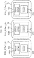
- FIG. 1A is a diagram schematically showing a configuration of an ECU before integration
- FIG. 1B is a diagram schematically showing a configuration of an integrated ECU of a comparative example.
- an ECU_A1a, an ECU_B1b, and an ECU_C1c before integration are mainly composed of semiconductor devices 10a, 10b, and 10c, respectively.
- Each of the semiconductor devices 10a, 10b, and 10c includes operation resources 100a, 100b, and 100c such as Central Processing Units (CPUs) and memories, and peripheral resources 200.
- the ECU_A1a, the ECU_B1b, and the ECU_C1c are developed and verified by different companies (Tier1_A, Tier1_B, and Tier1_C), respectively. Thereafter, it is assembled by the OEM.
- the integrated ECU 1R of the comparative example is mainly composed of a semiconductor device 10R.
- the semiconductor device 10R includes an operation resource 100 and a peripheral resource 200 for performing the functions of the ECU_A1a, the ECU_B1b, and the ECU_C1c.
- the operation resource 100 allocates one CPU and one memory to performance processing of the functions of ECU_Ala, ECU_B1b, and ECU_C1c in a time-division manner, and the peripheral resource 200 is shared.
- the integrated ECU 1R is developed and verified by the OEM, or any Tier1 of the Tier1_A, the Tier1_B and the Tier1_C, or another Tier1.
- software for realizing the functions of the ECU_A1a, the ECU_B1b and the ECU_C1c is developed and verified in each of Tier1_A, Tier1_B, and Tier1_C.
- FIG. 2A is a block diagram explaining verification of the integrated ECU of FIG. 1B by the Tier1
- FIG. 2B is a block diagram explaining verification of the integrated ECU of FIG. 1B by the OEM and the Tier1.
- FIG. 3 is a flowchart explaining verification of the integrated ECU of FIG. 1B .
- the verification of each single ECU function is often performed by the Tier1 responsible for development of each single ECU function, and the verification in the integrated state is performed by the OEM because of its nature. It is difficult for the OEM to perform the validation that the Tier1 performs. Therefore, the verification of the integrated ECU function is performed at the stage of (1) verification of the function and timing of the single ECU by each Tierl, and (2) verification in the state integrated by a plurality of ECU by the OEM.
- the Tier1_A, the Tier1_B, and the Tier1_C perform development and check of only software that each is in charge of by using the hardware of the integrated ECU 1R. That is, as shown in FIG. 3 , the Tier1_A develops the software for the function of the ECU_A (step SA1), and verifies the software for the function of the ECU_A (step SA2).
- the Tier1_B develops the software for the function of the ECU_B (step SB1), verifies the software for the function of the ECU_B (step SB2), the Tier1_C develops the software for the function of the ECU_C (step SC1), and verifies the software for the function of the ECU_C (step SC2).
- the OEM installs the software developed by the Tier1_A, the Tier1_B, and the Tier1_C together in the integrated ECU 1R and provided it to each Tier1 (step SO1).
- the Tier1_A checks (verifies) the operation of the software for the function of the ECU_A while operating the software for the function of the ECU_A, the software for the function of the ECU_B and the software for the function of the ECU_C in parallel (step SA3).
- the Tier1_B checks (verifies) the operation of the software for the function of the ECU_B (step SB3)
- the Tier1_C checks (verifies) the operation of the software for the function of ECU_C (step SC3).
- the OEM checks the operation in which the ECU_A, the ECU_B and the ECU_C cooperate (step SO2).
- the steps SA1, SA2, SB1, SB2, SC1 and SC2 are the same as the design and verification performed by the Tier1 for the ECUs that are not integrated.
- the steps SO1 and SO2 are the same as the verification performed by the OEM for the ECUs that are not integrated.
- the steps of SA3, SB3 and SC3 are the validations performed by the Tier1 that are increased by the integration. This is because of the following reason.
- peripheral resource 200 can be occupied in the case of the single ECU function evaluation, when the ECU integration is performed, the peripheral resource 200 is shared by each single ECU function. Therefore, although the verification of the function and timing of the single ECU is performed, the conflict of the peripheral resource 200 occurs, and therefore, it is required to confirm that the same operation as the operation at the time of the single ECU verification is performed even in the environment in which the functions are integrated. In other words, after the verification is performed alone, it is necessary to re-verify the state in which the functions are integrated.
- the Tier1 verifies the single ECU function, it is required to be able to perform the verification in a condition in which the peripheral resource is shared.
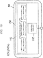
- FIG. 4 is a diagram schematically showing a configuration of the integrated ECU according to the embodiment.
- the integrated ECU 1 is mainly composed of a semiconductor device 10.
- the semiconductor device 10 includes an operation resource 100 for performing the functions of the ECU_A1a, the ECU_B1b and the ECU_C1c, a peripheral resource 200, and a control mechanism 300 for controlling the peripheral resource 200.
- the operation resource 100 allocates one CPU and one memory to processing of the operation resources 100a, 100b and 100c in a time-division manner, and the peripheral resource 200 is shared by the operation resources 100a, 100b, and 100c.
- the operation resource 100 may be configured by a plurality of CPUs.
- FIG. 5 is a diagram showing a usable period and a use prohibition period within a unit time.
- the control mechanism 300 creates a contended state by sharing the peripheral resource 200 at the time of the single ECU function verification of the above (1).
- the control mechanism 300 creates a use prohibition state corresponding to a budget value (BDG) allocated in advance to the shared peripheral resource 200, thereby realizing the verification of the single ECU within the use frequency achieved at the time of integration.
- a setting of the BDG is determined from restriction requirements for each single ECU (performance allocation of each single ECU).
- a period during which the peripheral resource 200 is in the use prohibition state is referred to as a use prohibition period UP, and a period during which the peripheral resource 200 is in a usable state is referred to as a usable period UA.
- a time of a unit time (UNIT TIME) is TU
- a time of the use prohibition period UP is TP
- the first time of the use prohibition period UP is TPa
- the second time of the use prohibition period UP is TPb
- a time of the usable period UA is TA
- T P TU/ (1+BDG).
- the time (TP) of the use prohibition period UP and the time (TA) of the usable period UA are determined based on the unit time (TU) and the budget value (BDG).
- the control mechanism 300 enables the peripheral resource 200 to be available only in a defined band at the time of the single ECU function evaluation.
- the control mechanism 300 may divide the usable period UA into the first usable period UA1, the second usable period UA2, the third usable period UA3 and the fourth usable period UA4, divide the use prohibition period UP into the first use prohibition period UP1, the second use prohibition period UP2, the third use prohibition period UP3, the fourth use prohibition period UP4 and the fifth usable prohibition period UP5, and cause the usable period UA to be dispersed.
- a time of the first usable period UA1 is TA1
- a time of the second usable period UA2 is TA2
- a time of the third usable period UA3 is TA3
- a time of the fourth usable period UA4 is TA4
- a time of the first use prohibition period UP1 is TP1
- a time of the second use prohibition period UP2 is TP2
- a time of the third use prohibition period UP3 is TP3
- a time of the fourth use prohibition period UP4 is TP4
- a time of the fifth use prohibition period UP5 is TP5,
- TA TA 1 + TA 2 + TA 3 + TA 4
- the use prohibition period is determined, for example, as follows:
- the single ECU function may not continuously access the peripheral resource 200 due to the constraint of its own processing content.
- the state in which this access is not performed is referred to as an inaccessible state, and the period is referred to as an inaccessible period. If there is no use of the peripheral resource 200 other than during the use prohibition period, the period during which such use had not been made may be deducted from the "the use prohibition period" and the inaccessible period potentially possessed by the single ECU function subject to the verification may not be recorded as the use prohibition period.
- the inaccessible period potentially possessed by the single ECU function subject to the verification is not included in the usable period, the inaccessible period potentially possessed by the single ECU function subject to the verification is recorded as the use prohibition period, and therefore, an excessive use prohibition period is not set.
- the control mechanism 300 may be configured by hardware or software.
- the peripheral resource is a circuit for realizing an input or output interface function for a semiconductor device such as Input/Output (I/O) to which a peripheral device such as a communication controller for communicating with another ECU and the like, a sensor, a switch, an actuator and the like is connected, and is a circuit that can be shared by a plurality of ECU functions.
- I/O Input/Output
- a peripheral device such as a communication controller for communicating with another ECU and the like, a sensor, a switch, an actuator and the like is connected
- FIG. 6 is a diagram schematically showing a configuration of an integrated ECU of the example.
- the integrated ECU 1A is connected to a Controller Area Network (CAN) bus 2a, which is an in-vehicle network, and can communicate with another ECU and the like.
- the integrated ECU 1A can be connected to a debugger 3 via a debugger interface (I/F) 4.
- I/F debugger interface
- the ECU 1A is mainly composed of a semiconductor device 10A, such as a microcontroller or a System-On-Chip (SOC), and a transceiver Integrated Circuit (IC) 20a.
- the semiconductor device 10A includes a CPU 101, a storage unit 102 for storing software programs 102a, 102b, and 102c for realizing each of the single ECU functions, a communication controller (communication peripheral circuit) 200a for CAN communication, a control circuit 300a, a control circuit 500 and a timer 600.
- a communication controller communication peripheral circuit
- the operation resource 100 is composed of the CPU 101 and the storage unit 102, and the CPU 101 executes the software programs 102a, 102b, and 102c stored in the storage unit 102 in a time-division manner to configure the functions of the ECU_A1a, the ECU_B1b and the ECU_C1c.
- the communication peripheral circuit 200a is shared similarly to the peripheral resource 200 of the embodiment.
- the operation resource 100 may be composed of a plurality of CPUs.
- the storage unit 102 includes, for example, a non-volatile memory, such as a flash memory, and a volatile memory, such as a Static Random Access Memory (SRAM).
- SRAM Static Random Access Memory
- the single ECU function is performed by the operation resource 100, and communicates an outside of the integrated ECU 1A through the communication peripheral circuit 200a as required.
- the communication peripheral circuit 200a converts a frame of a transmission buffer (not shown) into a serial transmission signal according to a communication protocol of the CAN, and outputs the serial transmission signal to the transceiver IC 20a.
- the transceiver IC 20a converts the transmission signal of a logic level obtained from the communication peripheral circuit 200a into a corresponding differential voltage and transmits the differential voltage to the CAN bus 2a.
- the transceiver IC 20a reads the differential voltage of the CAN bus 2a, and outputs a reception signal shaped to be included in a predetermined voltage range to the communication peripheral circuit 200a.
- a reception terminal of the communication peripheral circuit 200a includes, for example, a comparator, compares a predetermined threshold voltage with the reception signal from the transceiver IC 20a to generate digital data of "1" and "0", and stores the digital data in a reception buffer (not shown).
- the control circuit 300a sets the use prohibition period for the communication peripheral circuit 200a, and forms a contention state due to sharing in the communication peripheral circuit 200a.
- the use prohibition period is set in a state where the following conditions are satisfied.
- control circuit 300a the control circuit 300a:
- the communication peripheral circuit 200a is configured not to output an acknowledge signal in response to an access request signal from the CPU 101, for example, when the use prohibition is notified from the control circuit 300a, and the communication peripheral circuit 200a is configured to output an acknowledge signal when the usable state is notified.
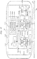
- FIG. 7 is a block diagram showing the configuration of the control circuit 300a of FIG. 6 .
- the control circuit 300a includes a counter 301 for measuring an operation time of the communication peripheral circuit 200a, and a main counter 302 for determining whether the communication peripheral circuit 200a is available or not.
- the counter 301 includes a counter register (CNTR) 301a, an incrementer (INC) 301b and a selector 301c.
- the counter 301 is initialized by assertion of a transfer end signal (SC1) from the communication peripheral circuit 200a or a reset signal (SC2) from the timer 600. This is performed by the selector 301c selecting "0" by the transfer end signal (SC1) or the reset signal (SC2) and inputting the selected "0" to the counter register (CNTR) 301a.
- the counter 301 continues to count up while the communication peripheral circuit 200a is operating.
- SC3 in-operation signal
- CNTR counter register
- the main counter 302 includes a main counter register (MCNTR) 302a, a decrementer (DEC) 302b, a selector 302c, a multiplier 302d, a register 302e, an adder 302f and a negative determiner 302g.
- the main counter 302 is initialized by the periodic reset signal (SC2). This is performed by the selector 302c selecting "0" by the reset signal (SC2) and inputting the selected "0" to the main counter register (MCNTR) 302a. It is assumed that a cycle of the reset signal (SC2) is a unit time (UNIT TIME) for which the allocated band is to be guaranteed when the communication peripheral circuit 200a is controlled.
- the main counter 302 operates as a subtraction counter when the communication peripheral circuit 200a is not operating. This is performed by the selector 302c selecting an output of the decrementer 302b in response to the in-operation signal (SC3) indicating that the communication peripheral circuit 200a is in operation and inputting the selected output of the decrementer 302b to the main counter register (MCNTR) 302a.
- SC3 in-operation signal
- MNTR main counter register
- the main counter 302 uses the multiplier 302d to multiply a value of the counter register (CNTR) 301a by the budget value (SC4) which is a coefficient (factor) set in advance in the register 302e by the control circuit 500, and adds the operation result to a value of the main counter register (MCNTR) 302a using the adder 302f. This is performed by the selector 302c selecting an output of the adder 302f in response to the transfer end signal (SC1) and inputting the selected output of the adder 302f to the main counter register (MCNTR) 302a.
- the negative determiner ( ⁇ 0) 302g determines whether the value of the main counter register (MCNTR) 302a is negative, and outputs an usable signal (SC5) to the communication peripheral circuit 200a. If the negative determiner 302g determines the value of the main counter register (MCNTR) 302a is negative, the usable signal (SC5) is asserted and the communication peripheral circuit 200a is available. If the negative determiner 302g determines the value of the main counter register (MCNTR) 302a is positive (is not negative), the usable signal (SC5) is negated and the communication peripheral circuit 200a is unavailable. The negative determiner 302g determines whether the value of the main counter register (MCNTR) 302a is negative, depending on whether the most significant bit of the main counter register (MCNTR) 302a is "1", for example.
- the budget value and the unit time (cycle) are set from the debugger 3 to the control circuit 300a via the debugger I/F 4.
- the settings are indicated by the OEM to the respective Tier1 with static values.
- the control circuit 500 sets the budget value (SC4) set by the debugger 3 in the register 302e of the control circuit 300a.
- the control circuit 500 sets the unit time set by the debugger 3 to the timer 600.
- the timer 600 generates the reset signal (SC1) every unit time.
- control circuit 300a the control circuit 500, the timer 600 and the debugger 3 are used only at the time of the unit ECU function evaluation by the Tierl, and are not used at the time of evaluation by the OEM or after mass production and shipping.
- FIG. 8 is a diagram for explaining the operation of the control circuit 300a of FIG. 6 .
- FIG. 9 is a diagram for explaining the operation of the control circuit 300a of FIG. 6 in a plurality of unit times.
- FIG. 8 shows an example in which the use (access request) ⁇ , ⁇ , and ⁇ of the communication peripheral circuit 200a occurs within the unit time (UNIT TIME).
- a usable period UA is set at the beginning of the unit time, the CPU 101 is unavailable to the communication peripheral circuit 200a, and after becoming available, an initial access request ⁇ is generated. It is assumed that a time taken to use the communication peripheral circuit 200a for the access request ⁇ is T ⁇ .
- a use prohibition period PB for the communication peripheral circuit 200a is set by the transfer end event signal (SC1) from the communication peripheral circuit 200a, and the main counter 302 starts to subtract.
- the communication peripheral circuit 200a While the value of the main counter register (MCNTR) 302a takes a positive value, the communication peripheral circuit 200a is disabled, and the use of the communication peripheral circuit 200a of the access request ⁇ generated until the value of the main counter register (MCNTR) 302a shows a negative number waits until the value of the main counter register (MCNTR) 302a becomes negative.
- the communication peripheral circuit 200a becomes available, and the use of the communication peripheral circuit 200a for the access request ⁇ starts.
- a time required for the use of the communication peripheral circuit 200a for the access request ⁇ is counted by the counter 301. During this time, the main counter 302 is not decremented and the values of the main counter register (MCNTR) 302a remain unchanged.
- a time (TC) of a use prohibition period PC of the communication peripheral circuit 200a is calculated again from the time (T ⁇ ) taken by the use of the communication peripheral circuit 200a for the access request ⁇ , and is added to the main counter register (MCNTR) 302a.
- the main counter 302 starts and continues the subtraction count process.
- the main counter 302 continues decrementing because there is no subsequent access request to the communication peripheral circuit 200a.
- the access request ⁇ can immediately start the use of the communication peripheral circuit 200a. This is because the value of the main counter register (MCNTR) 302a indicates a negative number.
- a time (TE) of a use prohibition period PE recalculated from the use of the communication peripheral circuit 200a for the access request ⁇ is calculated, and is added to the main counter register (MCNTR) 302a. Since the time (TE) of the use prohibition period PE calculated from the time (T ⁇ ) taken by the use of the communication peripheral circuit 200a for the access request ⁇ is added to the main counter register (MCNTR) 302a which is a negative number, the use prohibition period PE of the communication peripheral circuit 200a determined from the main counter register (MCNTR) 302a is the time (TE) obtained by subtracting a difference between the past time (TD) and the time (TC).
- the subsequent access request to the communication peripheral circuit 200a can be issued after the use prohibition period PE in which the above correction is performed has elapsed.
- the main counter 302 is initialized by the reset signal (SC2) regardless of the state of the main counter 302 after the elapse of the minimum unit time (UNIT TIME) for which the band guarantee of the communication peripheral circuit 200a is to be established.
- the first unit time in FIG. 9 an inaccessible period UN, a use period A, a use prohibition period P, ..., and an inaccessible period UN are set, and though the main counter register (MCNTR) 302a takes a negative number, the reset signal after the elapse of the unit time is inputted during the inaccessible period UN.
- the usable period UA includes the use period A and the inaccessible period UN.
- the inaccessible period UN of the first unit time continues.
- the reset signal after the elapse of the second unit time is also input during the inaccessible period UN.
- the use period A is set.
- the control circuit 300a initializes the main counter 302 every time a unit time elapses, and suppresses the occurrence of an access exceeding the budget allocation within the unit time.
- FIG. 10 is a flowchart explaining a manufacturing method of the integrated ECU 1A of FIG. 6 .
- the OEM develops and manufactures hardware of the integrated ECU 1A.
- the semiconductor device 10A in the integrated ECU 1A is manufactured by, for example, a semiconductor manufacturer or the like.
- the Tier1_A, the Tier1_B and the Tier1_C perform development and operation check of only the software that each is in charge of. That is, as shown in FIG. 10 , the Tier1_A develops the software for the function of the ECU_A (step SA11), verifies the software for the function of the ECU_A (step SA12), and delivers the software to the OEM.
- the Tier1_B develops the software for the function of the ECU_B (step SB11), verifies the software for the function of the ECU_B (step SB12), and delivers the software to the OEM.
- the Tier 1_C develops the software for the function of the ECU_C (step SC11), verifies the software for the function of the ECU_C (step SC12), and delivers the software to the OEM.
- the respective Tier1 can verify the function of the single ECU in the integrated state.
- the OEMs install the software developed and verified by Tier1_A, Tier1_B, and Tier1_C in the integrated ECU1 (step SO11).
- the OEM checks the operation of the ECU_A/ECU_B/ECU_C in cooperation with the ECU_A/ECU_B/ECU_C while operating the ECU_A, ECU_B, and ECU_C functions in parallel (step SO12). Note that the step SA3, SB3, SC3 of FIG. 3 by the Tier1 is not necessary between the step SO11 and the step SO12.
- the "control mechanism" for providing a certain "use prohibition period" to the communication peripheral circuit is mounted.
- the "use prohibition period” is determined in accordance with the past occupied time of the communication peripheral circuit as a target and the "band allocation" which is determined prior to the single ECU function evaluation. This function ensures that even in the integrated ECU, the processing within the "band” expected at the time of the integrated ECU is completed.
- the use prohibition period is set in cooperation with the immediately preceding use time of the communication peripheral circuit, the insertion of the use prohibition period is performed at discrete timing. It is possible to realize the single ECU evaluation while avoiding the use prohibition state of the communication peripheral circuit for a long period of time.
- the communication controller (communication peripheral circuit) for CAN communication is exemplified as the peripheral resource, but the communication peripheral circuit may be a circuit for FlexRay communication, Local Interconnect Network (LIN) communication, Ethernet communication, or the like.
- the number of peripheral resources is not limited to one, and a plurality of peripheral resources may be used.
- a case (modification) including two communication peripheral circuits of a communication controller for CAN communication and a communication controller for Ethernet communication will be described with reference to FIG. 11 .
- FIG. 11 is a diagram schematically showing a configuration of an integrated ECU of a modification.
- the integrated ECU 1B is connected to two in-vehicle network lines, i.e., a CAN bus 2a and an Ethernet bus 2b, which are in-vehicle networks, and can communicate with another ECU and the like.
- the integrated ECU 1B mainly is composed a semiconductor device 10B, such as a microcontroller or an SOC and transceiver ICs 20a and 20b.
- the semiconductor device 10B includes a CPU 101, a storage unit 102 storing software programs 102a, 102b, and 102c for realizing each single ECU function, a communication controller (communication peripheral circuit) 200a for CAN communication, a communication controller (communication peripheral circuit) 200b for Ethernet communication and control circuits 300a and 300b in one semiconductor chip.
- the operation resource 100 is composed of the CPU 101 and the storage unit 102, and the CPU 101 executes the software programs 102a, 102b, and 102c stored in the storage unit 102 in a time-division manner to configure the functions of the ECU_A1a, the ECU_B1, and the ECU_C1c.
- the communication peripheral circuits 200a and 200b are shared similarly to the peripheral resource 200 of the embodiment.
- the operation resource 100 may be composed of a plurality of CPUs.
- the storage unit 102 includes, for example, a non-volatile memory, such as a flash memory, and a volatile memory, such as SRAM.
- the single ECU function is performed by the operation resource 100, and communicates to an outside of the integrated ECU 1B through the communication peripheral circuits 200a and 200b as required.
Landscapes
- Engineering & Computer Science (AREA)
- Software Systems (AREA)
- Theoretical Computer Science (AREA)
- Physics & Mathematics (AREA)
- General Physics & Mathematics (AREA)
- Automation & Control Theory (AREA)
- General Engineering & Computer Science (AREA)
- Health & Medical Sciences (AREA)
- Mechanical Engineering (AREA)
- Artificial Intelligence (AREA)
- Computer Vision & Pattern Recognition (AREA)
- Evolutionary Computation (AREA)
- Medical Informatics (AREA)
- Debugging And Monitoring (AREA)
- Semiconductor Integrated Circuits (AREA)
- Test And Diagnosis Of Digital Computers (AREA)
- Microcomputers (AREA)
Abstract
Description
- The disclosure of Japanese Patent Application No.
2018-236819 - The present disclosure relates to a semiconductor device, and is applicable to a semiconductor device used, for example, in an Electronic Control Unit (ECU).
- Vehicles such as passenger cars, trucks, and buses are equipped with a large number of ECUs. Each ECU is interconnected and cooperates via an in-vehicle network. In-vehicle electronic architectures are becoming increasingly complex. To solve this problem, simplification of in-vehicle networks and integration of ECUs have been adopted as solutions for cost reduction in the entire in-vehicle electronic architecture (for example, Japanese unexamined Patent Application publication No.
2012-114724 - Individual systems (ECUs) subject to functional integration are developed and verified by different companies (Tier1) due to the business form. Here, the Tier1 is a primary supplier (primary subcontractor) that delivers products directly to a manufacturer. Thereafter, the vehicle is assembled by a vehicle manufacturer (hereinafter referred to as "OEM") that is in charge of vehicle assembly. At this time, the verification of the portion relating to the connection of each "individual system" is performed, and the verification of the function as a whole is completed. This is because the independence of "individual systems" is self-evident.
- On the other hand, it is expected that "systems" developed as "individual systems" will be integrated, but this integration also requires that the functions defined and verified as "individual systems" are reliably realized.
- Each Tier1 develops and verifies software that implements the ECU functions for which it is responsible using the hardware of the integrated ECU. The integrated ECU may be composed of a plurality of operation resources corresponding to a single ECU function and a peripheral resource shared by the plurality of operation resources. In this case, each operation resource cannot occupy the peripheral resource, and the use is limited.
- However, at the time of verification of the single ECU function in the integrated ECU, the peripheral resource is occupied, and the respective Tier1 cannot verify the single ECU function in the integrated state. Other objects and new features will be apparent from the description of this specification and the accompanying drawings.
- One typical aspect of the present disclosure will be briefly described below. A semiconductor device includes an operation resource which performs a plurality of ECU functions, a peripheral resource which is shared by the plurality of ECU functions, and a control mechanism which controls a period in which one of the ECU functions uses the peripheral resource. The control mechanism calculates, based on a budget value which is given in advance and is a performance allocation, a use prohibition period in which the one of the ECU functions is prohibited from using the peripheral resource within a predetermined unit time.
- According to the above semiconductor device, the single ECU function can be verified in the integrated state.
-
-
FIG. 1A is a diagram schematically showing a configuration of an ECU before integration. -
FIG. 1B is a diagram schematically showing a configuration of an integrated ECU of a comparative example. -
FIG. 2A is a block diagram explaining verification of the integrated ECU ofFIG. 1B by the Tier1. -
FIG. 2B is a block diagram explaining verification of the integrated ECU ofFIG. 1B by the OEM and the Tier1. -
FIG. 3 is a flowchart explaining verification of the integrated ECU ofFIG. 1B . -
FIG. 4 is a diagram schematically showing a configuration of an integrated ECU according to an embodiment. -
FIG. 5 is a diagram showing a usable period and a use prohibition period within a unit time. -
FIG. 6 is a diagram schematically showing a configuration of an integrated ECU of an example. -
FIG. 7 is a block diagram showing a configuration of the control circuit ofFIG. 6 . -
FIG. 8 is a diagram explaining an operation of a control circuit ofFIG. 6 . -
FIG. 9 is a diagram explaining the operation of the control circuit ofFIG. 6 in a plurality of unit times. -
FIG. 10 is a flowchart explaining a manufacturing method of the integrated ECU ofFIG. 6 . -
FIG. 11 is a diagram schematically showing a configuration of an integrated ECU of a modification. - An embodiment, an example and a modification will be described below with reference to the drawings. However, in the following description, the same components are denoted by the same reference numerals, and a repetitive description thereof may be omitted.
- First, a function integration of an ECU will be described with reference to
FIGS. 1A and1B .FIG. 1A is a diagram schematically showing a configuration of an ECU before integration, andFIG. 1B is a diagram schematically showing a configuration of an integrated ECU of a comparative example. - As shown in
FIG. 1A , an ECU_A1a, an ECU_B1b, and an ECU_C1c before integration are mainly composed ofsemiconductor devices semiconductor devices operation resources peripheral resources 200. The ECU_A1a, the ECU_B1b, and the ECU_C1c are developed and verified by different companies (Tier1_A, Tier1_B, and Tier1_C), respectively. Thereafter, it is assembled by the OEM. At this time, verification of portions relating to the respective connections of the ECU_A1a, the ECU_B1b, and the ECU_C1c is performed, and verification of the function as a whole is completed. This is because independence of the ECU_A1a, the ECU_B1b, and the ECU_C1c is self-evident. When the Tier1_A, the Tier1_B, and the Tier1_C are represented, they are referred to as the Tier1. - As shown in
FIG. 1B , the integratedECU 1R of the comparative example is mainly composed of asemiconductor device 10R. Thesemiconductor device 10R includes anoperation resource 100 and aperipheral resource 200 for performing the functions of the ECU_A1a, the ECU_B1b, and the ECU_C1c. For example, theoperation resource 100 allocates one CPU and one memory to performance processing of the functions of ECU_Ala, ECU_B1b, and ECU_C1c in a time-division manner, and theperipheral resource 200 is shared. The integratedECU 1R is developed and verified by the OEM, or any Tier1 of the Tier1_A, the Tier1_B and the Tier1_C, or another Tier1. However, software for realizing the functions of the ECU_A1a, the ECU_B1b and the ECU_C1c is developed and verified in each of Tier1_A, Tier1_B, and Tier1_C. - Problems occurring in the integrated
ECU 1R of the comparative example will be described with reference toFIGS. 2A ,2B and3 .FIG. 2A is a block diagram explaining verification of the integrated ECU ofFIG. 1B by the Tier1, andFIG. 2B is a block diagram explaining verification of the integrated ECU ofFIG. 1B by the OEM and the Tier1.FIG. 3 is a flowchart explaining verification of the integrated ECU ofFIG. 1B . - Generally, the verification of each single ECU function is often performed by the Tier1 responsible for development of each single ECU function, and the verification in the integrated state is performed by the OEM because of its nature. It is difficult for the OEM to perform the validation that the Tier1 performs. Therefore, the verification of the integrated ECU function is performed at the stage of (1) verification of the function and timing of the single ECU by each Tierl, and (2) verification in the state integrated by a plurality of ECU by the OEM.
- As shown in
FIGS. 2A and3 , in the verification of the above (1), the Tier1_A, the Tier1_B, and the Tier1_C perform development and check of only software that each is in charge of by using the hardware of the integratedECU 1R. That is, as shown inFIG. 3 , the Tier1_A develops the software for the function of the ECU_A (step SA1), and verifies the software for the function of the ECU_A (step SA2). Similarly, the Tier1_B develops the software for the function of the ECU_B (step SB1), verifies the software for the function of the ECU_B (step SB2), the Tier1_C develops the software for the function of the ECU_C (step SC1), and verifies the software for the function of the ECU_C (step SC2). - As shown in
FIGS. 2B and3 , in the verification of the above (2), the OEM installs the software developed by the Tier1_A, the Tier1_B, and the Tier1_C together in the integratedECU 1R and provided it to each Tier1 (step SO1). - Next, the Tier1_A checks (verifies) the operation of the software for the function of the ECU_A while operating the software for the function of the ECU_A, the software for the function of the ECU_B and the software for the function of the ECU_C in parallel (step SA3). Similarly, the Tier1_B checks (verifies) the operation of the software for the function of the ECU_B (step SB3), and the Tier1_C checks (verifies) the operation of the software for the function of ECU_C (step SC3). Finally, the OEM checks the operation in which the ECU_A, the ECU_B and the ECU_C cooperate (step SO2).
- The steps SA1, SA2, SB1, SB2, SC1 and SC2 are the same as the design and verification performed by the Tier1 for the ECUs that are not integrated. The steps SO1 and SO2 are the same as the verification performed by the OEM for the ECUs that are not integrated. The steps of SA3, SB3 and SC3 are the validations performed by the Tier1 that are increased by the integration. This is because of the following reason.
- Although the
peripheral resource 200 can be occupied in the case of the single ECU function evaluation, when the ECU integration is performed, theperipheral resource 200 is shared by each single ECU function. Therefore, although the verification of the function and timing of the single ECU is performed, the conflict of theperipheral resource 200 occurs, and therefore, it is required to confirm that the same operation as the operation at the time of the single ECU verification is performed even in the environment in which the functions are integrated. In other words, after the verification is performed alone, it is necessary to re-verify the state in which the functions are integrated. - In order to implement the integrated ECU in which a plurality of ECU functions are integrated, it is essential that the result of the verification performed in the above (1) can be used (the verification in the above (1) is unnecessary) when the verification is performed by integrating the plurality of ECU functions in the above (2). In other words, it is required to perform the verification of the above (1) so that the verification result of the above (1) can be utilized at the time of the verification of the above (2).
- Therefore, in the integrated ECU, when the Tier1 verifies the single ECU function, it is required to be able to perform the verification in a condition in which the peripheral resource is shared.
- An integrated ECU according to an embodiment in which the single ECU_A1a, the single ECU_B1b, and the single ECU_C1c of
FIG. 1A are integrated will be described with reference toFIG. 4. FIG. 4 is a diagram schematically showing a configuration of the integrated ECU according to the embodiment. - The
integrated ECU 1 according to the embodiment is mainly composed of asemiconductor device 10. Thesemiconductor device 10 includes anoperation resource 100 for performing the functions of the ECU_A1a, the ECU_B1b and the ECU_C1c, aperipheral resource 200, and acontrol mechanism 300 for controlling theperipheral resource 200. For example, theoperation resource 100 allocates one CPU and one memory to processing of theoperation resources peripheral resource 200 is shared by theoperation resources operation resource 100 may be configured by a plurality of CPUs. - Next, the function of the control mechanism of
FIG. 4 will be described with reference toFIG. 5. FIG. 5 is a diagram showing a usable period and a use prohibition period within a unit time. - The
control mechanism 300 creates a contended state by sharing theperipheral resource 200 at the time of the single ECU function verification of the above (1). - For example, the
control mechanism 300 creates a use prohibition state corresponding to a budget value (BDG) allocated in advance to the sharedperipheral resource 200, thereby realizing the verification of the single ECU within the use frequency achieved at the time of integration. A setting of the BDG is determined from restriction requirements for each single ECU (performance allocation of each single ECU). A period during which theperipheral resource 200 is in the use prohibition state is referred to as a use prohibition period UP, and a period during which theperipheral resource 200 is in a usable state is referred to as a usable period UA. Assuming that a time of a unit time (UNIT TIME) is TU, a time of the use prohibition period UP is TP, the first time of the use prohibition period UP is TPa, the second time of the use prohibition period UP is TPb, and a time of the usable period UA is TA,

- The time (TP) of the use prohibition period UP and the time (TA) of the usable period UA are determined based on the unit time (TU) and the budget value (BDG). As a result, the
control mechanism 300 enables theperipheral resource 200 to be available only in a defined band at the time of the single ECU function evaluation. - Since the
peripheral resource 200 may be discretely used within the budget value, it is not consistent with providing only one usable period. Thus, for example, thecontrol mechanism 300 may divide the usable period UA into the first usable period UA1, the second usable period UA2, the third usable period UA3 and the fourth usable period UA4, divide the use prohibition period UP into the first use prohibition period UP1, the second use prohibition period UP2, the third use prohibition period UP3, the fourth use prohibition period UP4 and the fifth usable prohibition period UP5, and cause the usable period UA to be dispersed. Here, when a time of the first usable period UA1 is TA1, a time of the second usable period UA2 is TA2, a time of the third usable period UA3 is TA3, a time of the fourth usable period UA4 is TA4, a time of the first use prohibition period UP1 is TP1, a time of the second use prohibition period UP2 is TP2, a time of the third use prohibition period UP3 is TP3, a time of the fourth use prohibition period UP4 is TP4, and a time of the fifth use prohibition period UP5 is TP5,

- The use prohibition period is determined, for example, as follows:
- (a) The use prohibition period of the
peripheral resource 200 is dynamically inserted based on a use time of theperipheral resource 200. The time of the use prohibition period is calculated based on the budget value. This makes it possible to provide the same use rate of the peripheral resource as in the integrated ECU when the single ECU function evaluation is performed. - (b) After the use of the
peripheral resource 200, the use prohibition period is set based on the use time, and inserted. Preferably, the use prohibition period (e.g., the first use prohibition period UP1 of the time (TP1)) is set based on an immediately preceding use time (e.g., the time (TA1) of the first usable period UA1), and inserted. As a result, it is possible to provide the single ECU function subject to the verification with an opportunity to discretely use the peripheral resource. - Moreover, the single ECU function may not continuously access the
peripheral resource 200 due to the constraint of its own processing content. The state in which this access is not performed is referred to as an inaccessible state, and the period is referred to as an inaccessible period. If there is no use of theperipheral resource 200 other than during the use prohibition period, the period during which such use had not been made may be deducted from the "the use prohibition period" and the inaccessible period potentially possessed by the single ECU function subject to the verification may not be recorded as the use prohibition period. Since the inaccessible period potentially possessed by the single ECU function subject to the verification is not included in the usable period, the inaccessible period potentially possessed by the single ECU function subject to the verification is recorded as the use prohibition period, and therefore, an excessive use prohibition period is not set. - The
control mechanism 300 may be configured by hardware or software. The peripheral resource is a circuit for realizing an input or output interface function for a semiconductor device such as Input/Output (I/O) to which a peripheral device such as a communication controller for communicating with another ECU and the like, a sensor, a switch, an actuator and the like is connected, and is a circuit that can be shared by a plurality of ECU functions. In the following example, a case in which thecontrol mechanism 300 according to the embodiment is configured by hardware and a case in which the peripheral resource is a communication controller will be described. -
FIG. 6 is a diagram schematically showing a configuration of an integrated ECU of the example. As shown inFIG. 6 , the integrated ECU 1A is connected to a Controller Area Network (CAN) bus 2a, which is an in-vehicle network, and can communicate with another ECU and the like. The integrated ECU 1A can be connected to adebugger 3 via a debugger interface (I/F) 4. - The ECU 1A is mainly composed of a
semiconductor device 10A, such as a microcontroller or a System-On-Chip (SOC), and a transceiver Integrated Circuit (IC) 20a. Thesemiconductor device 10A includes aCPU 101, astorage unit 102 for storingsoftware programs control circuit 300a, acontrol circuit 500 and atimer 600. Theoperation resource 100 is composed of theCPU 101 and thestorage unit 102, and theCPU 101 executes thesoftware programs storage unit 102 in a time-division manner to configure the functions of the ECU_A1a, the ECU_B1b and the ECU_C1c. The communicationperipheral circuit 200a is shared similarly to theperipheral resource 200 of the embodiment. Theoperation resource 100 may be composed of a plurality of CPUs. Thestorage unit 102 includes, for example, a non-volatile memory, such as a flash memory, and a volatile memory, such as a Static Random Access Memory (SRAM). - The single ECU function is performed by the
operation resource 100, and communicates an outside of the integrated ECU 1A through the communicationperipheral circuit 200a as required. - The communication
peripheral circuit 200a converts a frame of a transmission buffer (not shown) into a serial transmission signal according to a communication protocol of the CAN, and outputs the serial transmission signal to thetransceiver IC 20a. Thetransceiver IC 20a converts the transmission signal of a logic level obtained from the communicationperipheral circuit 200a into a corresponding differential voltage and transmits the differential voltage to the CAN bus 2a. - At the time of data reception, the
transceiver IC 20a reads the differential voltage of the CAN bus 2a, and outputs a reception signal shaped to be included in a predetermined voltage range to the communicationperipheral circuit 200a. A reception terminal of the communicationperipheral circuit 200a includes, for example, a comparator, compares a predetermined threshold voltage with the reception signal from thetransceiver IC 20a to generate digital data of "1" and "0", and stores the digital data in a reception buffer (not shown). - The
control circuit 300a sets the use prohibition period for the communicationperipheral circuit 200a, and forms a contention state due to sharing in the communicationperipheral circuit 200a. The use prohibition period is set in a state where the following conditions are satisfied. - (I) Considering that allocation to other processes is prioritized immediately after use
- (II) considering the inaccessible state of the single ECU itself
- In particular, the
control circuit 300a: - (A) notifies the communication
peripheral circuit 200a of the use prohibition/usable state, and sets the communicationperipheral circuit 200a to the use prohibition state; - (B) calculates the use prohibition state of the communication
peripheral circuit 200a by a predetermined constraint (budget value); - (C) sets a period (use prohibition period) of the next use prohibition state by the predetermined constraint (budget value) and a use time of the communication
peripheral circuit 200a operated in the past; and - (D) removes the inaccessible time for the communication
peripheral circuit 200a from the use prohibition period. - The communication
peripheral circuit 200a is configured not to output an acknowledge signal in response to an access request signal from theCPU 101, for example, when the use prohibition is notified from thecontrol circuit 300a, and the communicationperipheral circuit 200a is configured to output an acknowledge signal when the usable state is notified. - Next, a configuration of the
control circuit 300a will be described with reference toFIG. 7. FIG. 7 is a block diagram showing the configuration of thecontrol circuit 300a ofFIG. 6 . - The
control circuit 300a includes acounter 301 for measuring an operation time of the communicationperipheral circuit 200a, and amain counter 302 for determining whether the communicationperipheral circuit 200a is available or not. Thecontrol circuit 300a: - (i) down-counts the
main counter 302 during a period in which the communicationperipheral circuit 200a is not used; - (ii) makes the communication
peripheral circuit 200a available when a count value of themain counter 302 is negative, and disables the communicationperipheral circuit 200a when the count value is positive; - (iii) stops the
main counter 302 while the communicationperipheral circuit 200a is used; and - (iv) after the communication
peripheral circuit 200a is used, adds the count value of themain counter 302 in accordance with a use rate. - The
counter 301 includes a counter register (CNTR) 301a, an incrementer (INC) 301b and aselector 301c. Thecounter 301 is initialized by assertion of a transfer end signal (SC1) from the communicationperipheral circuit 200a or a reset signal (SC2) from thetimer 600. This is performed by theselector 301c selecting "0" by the transfer end signal (SC1) or the reset signal (SC2) and inputting the selected "0" to the counter register (CNTR) 301a. Thecounter 301 continues to count up while the communicationperipheral circuit 200a is operating. This is performed by theselector 301c selecting an output of theincrementer 301b in response to an in-operation signal (SC3) indicating that the communicationperipheral circuit 200a is in operation and inputting the selected output of the incrementer 301b to the counter register (CNTR) 301a. As a result, when the transfer end signal (SC1) is generated, thecounter 301 indicates an occupied time in which the communicationperipheral circuit 200a is used. - The
main counter 302 includes a main counter register (MCNTR) 302a, a decrementer (DEC) 302b, aselector 302c, amultiplier 302d, aregister 302e, anadder 302f and anegative determiner 302g. Themain counter 302 is initialized by the periodic reset signal (SC2). This is performed by theselector 302c selecting "0" by the reset signal (SC2) and inputting the selected "0" to the main counter register (MCNTR) 302a. It is assumed that a cycle of the reset signal (SC2) is a unit time (UNIT TIME) for which the allocated band is to be guaranteed when the communicationperipheral circuit 200a is controlled. - The
main counter 302 operates as a subtraction counter when the communicationperipheral circuit 200a is not operating. This is performed by theselector 302c selecting an output of thedecrementer 302b in response to the in-operation signal (SC3) indicating that the communicationperipheral circuit 200a is in operation and inputting the selected output of the decrementer 302b to the main counter register (MCNTR) 302a. - When the transfer end signal (SC1) is generated, the
main counter 302 uses themultiplier 302d to multiply a value of the counter register (CNTR) 301a by the budget value (SC4) which is a coefficient (factor) set in advance in theregister 302e by thecontrol circuit 500, and adds the operation result to a value of the main counter register (MCNTR) 302a using theadder 302f. This is performed by theselector 302c selecting an output of theadder 302f in response to the transfer end signal (SC1) and inputting the selected output of theadder 302f to the main counter register (MCNTR) 302a. - The negative determiner (<0) 302g determines whether the value of the main counter register (MCNTR) 302a is negative, and outputs an usable signal (SC5) to the communication
peripheral circuit 200a. If thenegative determiner 302g determines the value of the main counter register (MCNTR) 302a is negative, the usable signal (SC5) is asserted and the communicationperipheral circuit 200a is available. If thenegative determiner 302g determines the value of the main counter register (MCNTR) 302a is positive (is not negative), the usable signal (SC5) is negated and the communicationperipheral circuit 200a is unavailable. Thenegative determiner 302g determines whether the value of the main counter register (MCNTR) 302a is negative, depending on whether the most significant bit of the main counter register (MCNTR) 302a is "1", for example. - As shown in
FIG. 6 , the budget value and the unit time (cycle) are set from thedebugger 3 to thecontrol circuit 300a via the debugger I/F 4. The settings are indicated by the OEM to the respective Tier1 with static values. Thecontrol circuit 500 sets the budget value (SC4) set by thedebugger 3 in theregister 302e of thecontrol circuit 300a. Thecontrol circuit 500 sets the unit time set by thedebugger 3 to thetimer 600. Thetimer 600 generates the reset signal (SC1) every unit time. - Note that the
control circuit 300a, thecontrol circuit 500, thetimer 600 and thedebugger 3 are used only at the time of the unit ECU function evaluation by the Tierl, and are not used at the time of evaluation by the OEM or after mass production and shipping. - Next, an operation of the
control circuit 300a will be described in detail with reference toFIGS. 8 and9 .FIG. 8 is a diagram for explaining the operation of thecontrol circuit 300a ofFIG. 6 .FIG. 9 is a diagram for explaining the operation of thecontrol circuit 300a ofFIG. 6 in a plurality of unit times.FIG. 8 shows an example in which the use (access request) α, β, and γ of the communicationperipheral circuit 200a occurs within the unit time (UNIT TIME). - Although a usable period UA is set at the beginning of the unit time, the
CPU 101 is unavailable to the communicationperipheral circuit 200a, and after becoming available, an initial access request α is generated. It is assumed that a time taken to use the communicationperipheral circuit 200a for the access request α is Tα. - A use prohibition period PB for the communication
peripheral circuit 200a is set by the transfer end event signal (SC1) from the communicationperipheral circuit 200a, and themain counter 302 starts to subtract. - While the value of the main counter register (MCNTR) 302a takes a positive value, the communication
peripheral circuit 200a is disabled, and the use of the communicationperipheral circuit 200a of the access request β generated until the value of the main counter register (MCNTR) 302a shows a negative number waits until the value of the main counter register (MCNTR) 302a becomes negative. - A time (TB) of the use prohibition period PB of the communication
peripheral circuit 200a is derived from the time (Tα) taken for the processing at the time of the immediately preceding use for the communicationperipheral circuit 200a. If the use allocation (coefficient (factor)) of the communicationperipheral circuit 200a to the single ECU function to be targeted is K%, the value of TB is derived from a time obtained by multiplying Tα by (100-K)/K. For example, when K=25, TB=3×Tα. - When the value of the main counter register (MCNTR) 302a becomes a negative value, the communication
peripheral circuit 200a becomes available, and the use of the communicationperipheral circuit 200a for the access request β starts. - A time required for the use of the communication
peripheral circuit 200a for the access request β is counted by thecounter 301. During this time, themain counter 302 is not decremented and the values of the main counter register (MCNTR) 302a remain unchanged. - A time (TC) of a use prohibition period PC of the communication
peripheral circuit 200a is calculated again from the time (Tβ) taken by the use of the communicationperipheral circuit 200a for the access request β, and is added to the main counter register (MCNTR) 302a. Themain counter 302 starts and continues the subtraction count process. - Although the usable period UA is set after the time (TC) of the use prohibition period PC has elapsed, the
main counter 302 continues decrementing because there is no subsequent access request to the communicationperipheral circuit 200a. - If the access request γ occurs after the elapse of a TD time (longer than the TC time) from the previous access request β, the access request γ can immediately start the use of the communication
peripheral circuit 200a. This is because the value of the main counter register (MCNTR) 302a indicates a negative number. - After the use of the communication
peripheral circuit 200a for the access request γ is completed, a time (TE) of a use prohibition period PE recalculated from the use of the communicationperipheral circuit 200a for the access request γ is calculated, and is added to the main counter register (MCNTR) 302a. Since the time (TE) of the use prohibition period PE calculated from the time (Tγ) taken by the use of the communicationperipheral circuit 200a for the access request γ is added to the main counter register (MCNTR) 302a which is a negative number, the use prohibition period PE of the communicationperipheral circuit 200a determined from the main counter register (MCNTR) 302a is the time (TE) obtained by subtracting a difference between the past time (TD) and the time (TC). The subsequent access request to the communicationperipheral circuit 200a can be issued after the use prohibition period PE in which the above correction is performed has elapsed. - As shown in
FIG. 9 , themain counter 302 is initialized by the reset signal (SC2) regardless of the state of themain counter 302 after the elapse of the minimum unit time (UNIT TIME) for which the band guarantee of the communicationperipheral circuit 200a is to be established. In the first unit time inFIG. 9 , an inaccessible period UN, a use period A, a use prohibition period P, ..., and an inaccessible period UN are set, and though the main counter register (MCNTR) 302a takes a negative number, the reset signal after the elapse of the unit time is inputted during the inaccessible period UN. Here, the usable period UA includes the use period A and the inaccessible period UN. At the beginning of the second unit time, the inaccessible period UN of the first unit time continues. The reset signal after the elapse of the second unit time is also input during the inaccessible period UN. However, at the beginning of the third unit time, the use period A is set. Thecontrol circuit 300a initializes themain counter 302 every time a unit time elapses, and suppresses the occurrence of an access exceeding the budget allocation within the unit time. -
FIG. 10 is a flowchart explaining a manufacturing method of the integrated ECU 1A ofFIG. 6 . The OEM develops and manufactures hardware of the integrated ECU 1A. Thesemiconductor device 10A in the integrated ECU 1A is manufactured by, for example, a semiconductor manufacturer or the like. Using the hardware of the integrated ECU 1A lent from the OEM, the Tier1_A, the Tier1_B and the Tier1_C perform development and operation check of only the software that each is in charge of. That is, as shown inFIG. 10 , the Tier1_A develops the software for the function of the ECU_A (step SA11), verifies the software for the function of the ECU_A (step SA12), and delivers the software to the OEM. Similarly, the Tier1_B develops the software for the function of the ECU_B (step SB11), verifies the software for the function of the ECU_B (step SB12), and delivers the software to the OEM. The Tier 1_C develops the software for the function of the ECU_C (step SC11), verifies the software for the function of the ECU_C (step SC12), and delivers the software to the OEM. The respective Tier1 can verify the function of the single ECU in the integrated state. - As shown in
FIG. 10 , the OEMs install the software developed and verified by Tier1_A, Tier1_B, and Tier1_C in the integrated ECU1 (step SO11). The OEM checks the operation of the ECU_A/ECU_B/ECU_C in cooperation with the ECU_A/ECU_B/ECU_C while operating the ECU_A, ECU_B, and ECU_C functions in parallel (step SO12). Note that the step SA3, SB3, SC3 ofFIG. 3 by the Tier1 is not necessary between the step SO11 and the step SO12. - In this example, in the semiconductor provided for the integrated ECU, the "control mechanism" for providing a certain "use prohibition period" to the communication peripheral circuit is mounted.
- Further, the "use prohibition period" is determined in accordance with the past occupied time of the communication peripheral circuit as a target and the "band allocation" which is determined prior to the single ECU function evaluation. This function ensures that even in the integrated ECU, the processing within the "band" expected at the time of the integrated ECU is completed.
- Further, since the use prohibition period is set in cooperation with the immediately preceding use time of the communication peripheral circuit, the insertion of the use prohibition period is performed at discrete timing. It is possible to realize the single ECU evaluation while avoiding the use prohibition state of the communication peripheral circuit for a long period of time.
- By subtracting the potential inaccessible period of the single ECU function from the "use prohibition period" set by the control circuit, it is avoided that the use prohibition period is set excessively. This is because, when operating as the integrated ECU, accesses from other single ECU functions can be executed even during the "use prohibition period" of the single ECU function.
- Several exemplary modifications will be illustrated below. In the following explanation of the modification, the same reference numerals as those of the above-mentioned example may be used for components having the same structures and functions as those described in the above-mentioned example. In the description of such portions, the description in the above-mentioned example can be appropriately incorporated within the scope not inconsistent with the technical aspects. In addition, a part of the above-mentioned example and all or a part of a plurality of modifications may be applied in combination as appropriate within the scope not inconsistent with the technical aspects.
- In the example, the communication controller (communication peripheral circuit) for CAN communication is exemplified as the peripheral resource, but the communication peripheral circuit may be a circuit for FlexRay communication, Local Interconnect Network (LIN) communication, Ethernet communication, or the like. The number of peripheral resources is not limited to one, and a plurality of peripheral resources may be used. Hereinafter, a case (modification) including two communication peripheral circuits of a communication controller for CAN communication and a communication controller for Ethernet communication will be described with reference to
FIG. 11 . -
FIG. 11 is a diagram schematically showing a configuration of an integrated ECU of a modification. - As shown in
FIG. 11 , the integrated ECU 1B is connected to two in-vehicle network lines, i.e., a CAN bus 2a and an Ethernet bus 2b, which are in-vehicle networks, and can communicate with another ECU and the like. The integrated ECU 1B mainly is composed asemiconductor device 10B, such as a microcontroller or an SOC andtransceiver ICs semiconductor device 10B includes aCPU 101, astorage unit 102storing software programs control circuits operation resource 100 is composed of theCPU 101 and thestorage unit 102, and theCPU 101 executes thesoftware programs storage unit 102 in a time-division manner to configure the functions of the ECU_A1a, the ECU_B1, and the ECU_C1c. The communicationperipheral circuits 200a and 200b are shared similarly to theperipheral resource 200 of the embodiment. Theoperation resource 100 may be composed of a plurality of CPUs. Thestorage unit 102 includes, for example, a non-volatile memory, such as a flash memory, and a volatile memory, such as SRAM. - The single ECU function is performed by the
operation resource 100, and communicates to an outside of the integrated ECU 1B through the communicationperipheral circuits 200a and 200b as required. - Although the invention made by the present inventor has been specifically described based on the embodiment, example and modification, it is needless to say that the present invention is not limited to the above-described embodiment, example and modification, and can be variously modified.
- For example, in the embodiment, example and modification, the case in which three single ECU functions are integrated has been described, but the present invention is not limited to this, and can be applied to a case in which two or more single ECU functions are integrated.
Claims (11)
- A semiconductor device comprising:an operation resource configured to perform a plurality of Electronic Control Unit (ECU) functions;a peripheral resource configured to be shared by the plurality of ECU functions; anda control mechanism configured to control a period in which one of the ECU functions uses the peripheral resource,wherein the control mechanism is configured to calculate, based on a budget value which is given in advance and is a performance allocation, a use prohibition period in which the one of the ECU functions is prohibited from using the peripheral resource within a predetermined unit time.
- The semiconductor device according to Claim 1, wherein the control mechanism is configured to dynamically calculate the use prohibition period based on a use time in which the one of the ECU functions uses the peripheral resources.
- The semiconductor device according to Claim 1 or 2, wherein the control mechanism is configured to calculate the use prohibition period based on an immediately preceding use time of the peripheral resource after the one of the ECU functions uses the peripheral resource.
- The semiconductor device according to any one of Claims 1 to 3, wherein, when there is a period in which the peripheral resource is not used by the one of the ECU functions in a period other than the use prohibition period, the control mechanism is configured to subtract the period in which the peripheral resource is not used by the one of the ECU functions from the use prohibition period.
- The semiconductor device according to any one of Claims 1 to 4,
wherein the control mechanism comprises:a first counter configured to measure the use time in which one of the ECU functions uses the peripheral resource; anda second counter configured to determine availability and non-availability of the peripheral resource by the one of the ECU functions,wherein the control mechanism is configured to:add a value based on the budget value and a count value of the first counter to a count value of the second counter;decrease the count value of the second counter based on the period in which the peripheral resource is not used by the one of the ECU functions;if the count value of the second counter is positive, prohibit the one of the ECU functions from using the peripheral resource;if the count value of the second counter is negative, allow the one of the ECU functions to use the peripheral resource; andwhile the one of the ECU functions is using the peripheral resource, stop a counting operation of the second counter. - The semiconductor device according to any one of Claims 1 to 5, wherein the control mechanism further comprises:a timer configured to count the predetermined unit time, and to generate a signal for initializing the count value of the first counter and the count value of the second counter; anda control circuit configured to receive the budget value and the predetermined unit time from an outside.
- The semiconductor device according to any one of Claims 1 to 6,
wherein the operation resource comprises a memory which stores a software program and a Central Processing Unit (CPU) which executes the software program,
wherein the ECU functions are performed by the CPU executing the software program, and
wherein the peripheral resource comprises a communication peripheral circuit. - An ECU comprising:the semiconductor device according to any one of Claims 1 to 7; anda transceiver integrated circuit coupled to an in-vehicle network line and the communication peripheral circuit.
- The semiconductor device according to any one of Claims 1 to 8,
wherein the peripheral resource comprises a first peripheral resource,
wherein the control mechanism comprises a first control mechanism,
wherein the budget value comprises a first budget value,
wherein the use prohibition period comprises a first use prohibition period,
wherein the semiconductor device further comprises:a second peripheral resource configured to be shared by the plurality of ECU functions; anda second control mechanism configured to control a period in which one of the ECU functions uses the second peripheral resource,wherein the second control mechanism is configured to calculate, based on a second budget value which is given in advance and is a performance allocation, a second use prohibition period in which the one of the ECU functions is prohibited from using the second peripheral resource within a predetermined unit time. - A verification method of an Electronic Control Unit (ECU), comprising:providing the ECU which comprises a semiconductor device which includes an operation resource which performs a plurality of ECU functions, a peripheral resource which is shared by the plurality of ECU functions, and a control mechanism which controls a period in which one of the ECU functions uses the peripheral resource by calculating, based on a budget value which is given in advance and is a performance allocation, a use prohibition period in which the one of the ECU functions is prohibited from using the peripheral resource within a predetermined unit time;developing a software program for realizing the one of the ECU functions to incorporate the software program into the ECU; andoperating the ECU to verify the software program.
- A manufacturing method of an Electronic Control Unit (ECU), comprising:providing the ECU which comprises a semiconductor device which includes an operation resource which performs a plurality of ECU functions, a peripheral resource which is shared by the plurality of ECU functions, and a control mechanism which controls a period in which one of the ECU functions uses the peripheral resource by calculating, based on a budget value which is given in advance and is a performance allocation, a use prohibition period in which the one of the ECU functions is prohibited from using the peripheral resource within a predetermined unit time;providing a first software program verified by operating the ECU into which the first software program for realizing one of the plurality of ECU functions is incorporated;providing a second software program verified by operating the ECU into which the second software program for realizing another one of the plurality of ECU functions is incorporated; andincorporating the first and second software programs into the ECU to verify a cooperation function between the first and second software programs.
Applications Claiming Priority (1)
| Application Number | Priority Date | Filing Date | Title |
|---|---|---|---|
| JP2018236819A JP7141942B2 (en) | 2018-12-18 | 2018-12-18 | Semiconductor equipment and electronic control equipment |
Publications (2)
| Publication Number | Publication Date |
|---|---|
| EP3671446A1 true EP3671446A1 (en) | 2020-06-24 |
| EP3671446B1 EP3671446B1 (en) | 2025-01-22 |
Family
ID=68655292
Family Applications (1)
| Application Number | Title | Priority Date | Filing Date |
|---|---|---|---|
| EP19211093.0A Active EP3671446B1 (en) | 2018-12-18 | 2019-11-25 | Semiconductor device, electronic control unit, verification method of electronic control unit and manufacturing method of electronic control unit |
Country Status (4)
| Country | Link |
|---|---|
| US (2) | US11358546B2 (en) |
| EP (1) | EP3671446B1 (en) |
| JP (1) | JP7141942B2 (en) |
| CN (1) | CN111338314B (en) |
Families Citing this family (1)
| Publication number | Priority date | Publication date | Assignee | Title |
|---|---|---|---|---|
| CN111766848B (en) * | 2020-06-29 | 2021-09-10 | 北京广利核系统工程有限公司 | Method and device for verifying failure rate of subsystem in instrument control system |
Citations (1)
| Publication number | Priority date | Publication date | Assignee | Title |
|---|---|---|---|---|
| JP2012114724A (en) | 2010-11-25 | 2012-06-14 | Toyota Motor Corp | Electronic control device |
Family Cites Families (26)
| Publication number | Priority date | Publication date | Assignee | Title |
|---|---|---|---|---|
| JP2001282710A (en) | 2000-03-31 | 2001-10-12 | Brother Ind Ltd | Circuit and method for arbitrating bus use |
| US7353217B2 (en) * | 2001-06-01 | 2008-04-01 | Texas Instruments Incorporated | Intelligent realtime management of processing resources |
| KR100606946B1 (en) * | 2001-11-30 | 2006-08-01 | 후지쓰 텐 가부시키가이샤 | Microcomputer logic development device |
| JP4282472B2 (en) * | 2003-12-26 | 2009-06-24 | 株式会社東芝 | Microprocessor |
| JP4552982B2 (en) * | 2007-08-03 | 2010-09-29 | 株式会社デンソー | Electronic control unit |
| US20090217280A1 (en) * | 2008-02-21 | 2009-08-27 | Honeywell International Inc. | Shared-Resource Time Partitioning in a Multi-Core System |
| JP4624448B2 (en) * | 2008-07-30 | 2011-02-02 | 株式会社オートネットワーク技術研究所 | Control device, control system, and computer program |
| JP2011028559A (en) | 2009-07-27 | 2011-02-10 | Denso Corp | Relay program and electronic control device |
| CN101996146B (en) * | 2009-08-26 | 2013-08-07 | 戴尔产品有限公司 | Multi-mode processing module and using method thereof |
| JP2011216004A (en) | 2010-04-01 | 2011-10-27 | Toyota Motor Corp | Microprocessor, electronic control unit, execution ratio switching method |
| JP5850774B2 (en) * | 2012-03-22 | 2016-02-03 | ルネサスエレクトロニクス株式会社 | Semiconductor integrated circuit device and system using the same |
| US10643403B2 (en) * | 2012-08-20 | 2020-05-05 | Innova Electronics Corporation | Predictive diagnostic method and system |
| JP5870968B2 (en) * | 2013-06-03 | 2016-03-01 | 株式会社デンソー | Wire harness evaluation device |
| US9372725B2 (en) | 2014-02-19 | 2016-06-21 | International Business Machines Corporation | Dynamically adjusting wait periods according to system performance |
| US20160323283A1 (en) * | 2015-04-30 | 2016-11-03 | Samsung Electronics Co., Ltd. | Semiconductor device for controlling access right to resource based on pairing technique and method thereof |
| KR20160129663A (en) * | 2015-04-30 | 2016-11-09 | 삼성전자주식회사 | Semiconductor device of controlling access right for resource based on pairing technigue and method thereof |
| JP2017177410A (en) * | 2016-03-29 | 2017-10-05 | 富士ゼロックス株式会社 | Control device and printer |
| WO2018096755A1 (en) * | 2016-11-25 | 2018-05-31 | 株式会社デンソー | Parallel processing device and parallel processing program |
| EP3343366B1 (en) * | 2016-12-27 | 2020-12-30 | OpenSynergy GmbH | System and method for scheduling a plurality of guest systems and/or threads |
| US10055260B2 (en) * | 2017-01-05 | 2018-08-21 | Guardknox Cyber Technologies Ltd. | Specially programmed computing systems with associated devices configured to implement centralized services ECU based on services oriented architecture and methods of use thereof |
| US10664413B2 (en) * | 2017-01-27 | 2020-05-26 | Lear Corporation | Hardware security for an electronic control unit |
| JP7006461B2 (en) * | 2018-04-02 | 2022-01-24 | 株式会社デンソー | Electronic control device and electronic control system |
| EP3572939A1 (en) * | 2018-05-25 | 2019-11-27 | TTTech Auto AG | Method, device and real-time network for highly-integrated automotive systems |
| US20210358025A1 (en) * | 2020-05-15 | 2021-11-18 | Toyota Motor Engineering & Manufacturing North America, Inc. | Vehicle sharing systems and methods for matching available vehicles to user requests |
| US11614962B2 (en) * | 2020-06-25 | 2023-03-28 | Toyota Motor Engineering & Manufacturing North America, Inc. | Scheduling vehicle task offloading and triggering a backoff period |
| US11531566B2 (en) * | 2020-07-10 | 2022-12-20 | Infineon Technologies Ag | Safe and secure communication network message processing |
-
2018
- 2018-12-18 JP JP2018236819A patent/JP7141942B2/en active Active
-
2019
- 2019-11-06 US US16/676,047 patent/US11358546B2/en active Active
- 2019-11-19 CN CN201911135160.6A patent/CN111338314B/en active Active
- 2019-11-25 EP EP19211093.0A patent/EP3671446B1/en active Active
-
2022
- 2022-05-16 US US17/745,253 patent/US11845387B2/en active Active
Patent Citations (1)
| Publication number | Priority date | Publication date | Assignee | Title |
|---|---|---|---|---|
| JP2012114724A (en) | 2010-11-25 | 2012-06-14 | Toyota Motor Corp | Electronic control device |
Non-Patent Citations (2)
| Title |
|---|
| BECKERT MATTHIAS ET AL: "Exploiting sporadic servers to provide budget scheduling for ARINC653 based real-time virtualization environments", DESIGN, AUTOMATION & TEST IN EUROPE CONFERENCE & EXHIBITION (DATE), 2017, EDAA, 27 March 2017 (2017-03-27), pages 870 - 875, XP033096475, DOI: 10.23919/DATE.2017.7927109 * |
| THOMAS NOLTE ET AL: "A Synchronization Protocol for Temporal Isolation of Software Components in Vehicular Systems", IEEE TRANSACTIONS ON INDUSTRIAL INFORMATICS, IEEE SERVICE CENTER, NEW YORK, NY, US, vol. 5, no. 4, 13 October 2009 (2009-10-13), pages 375 - 387, XP011278351, ISSN: 1551-3203, DOI: 10.1109/TII.2009.2033267 * |
Also Published As
| Publication number | Publication date |
|---|---|
| JP7141942B2 (en) | 2022-09-26 |
| CN111338314A (en) | 2020-06-26 |
| US20220274546A1 (en) | 2022-09-01 |
| US11845387B2 (en) | 2023-12-19 |
| JP2020098507A (en) | 2020-06-25 |
| CN111338314B (en) | 2024-07-16 |
| EP3671446B1 (en) | 2025-01-22 |
| US20200189497A1 (en) | 2020-06-18 |
| US11358546B2 (en) | 2022-06-14 |
Similar Documents
| Publication | Publication Date | Title |
|---|---|---|
| EP3343373B1 (en) | Semiconductor device comprising watchdog timer | |
| CN108139945B (en) | Vehicle safety electronic control system | |
| CN115384535B (en) | Vehicle functional safety monitoring system and method | |
| US8509989B2 (en) | Monitoring concept in a control device | |
| US9068527B2 (en) | Monitoring computer in a control device | |
| EP3671446B1 (en) | Semiconductor device, electronic control unit, verification method of electronic control unit and manufacturing method of electronic control unit | |
| US6816827B1 (en) | Verification method for combinational loop systems | |
| JP2002158567A (en) | Generation of pulse signal from clock signal | |
| US20210328624A1 (en) | Relay device, relay method, and computer program | |
| US20040044839A1 (en) | Memory control apparatus and method for controlling memory access capable of selecting desirable page mode | |
| JP4425598B2 (en) | Arbitration parameter generation circuit, bus use parameter generation circuit, system on chip, arbitration parameter generation method, and bus use parameter generation method | |
| JP7803236B2 (en) | control device | |
| US20200341763A1 (en) | Secure element with personalizable functions and corresponding management method | |
| JP2012043315A (en) | Data processing system | |
| KR102806701B1 (en) | Control device and method for activating occupant protection means of a vehicle | |
| WO2021106353A1 (en) | Electronic control device | |
| EP3971721B1 (en) | Information processing device | |
| KR102958105B1 (en) | Method to optimize the transmission data rate of a sensor network in partial network operation of an Ethernet network | |
| JP6533489B2 (en) | Vehicle controller | |
| JP7056205B2 (en) | Microcomputer, electronic control device | |
| CN120826896A (en) | Communication system | |
| Jersak | New kid on the block: Scheduling Analysis improves quality and reliability of ECUs, Busses and Networks | |
| JP2026023842A (en) | Information processing device, in-vehicle system, information processing method, and computer program | |
| CN119380462A (en) | Vehicle locking time calibration method, device and engineering machinery | |
| US20180341312A1 (en) | Control apparatus, method for controlling the same, storage medium, and computer system |
Legal Events
| Date | Code | Title | Description |
|---|---|---|---|
| PUAI | Public reference made under article 153(3) epc to a published international application that has entered the european phase |
Free format text: ORIGINAL CODE: 0009012 |
|
| STAA | Information on the status of an ep patent application or granted ep patent |
Free format text: STATUS: THE APPLICATION HAS BEEN PUBLISHED |
|
| AK | Designated contracting states |
Kind code of ref document: A1 Designated state(s): AL AT BE BG CH CY CZ DE DK EE ES FI FR GB GR HR HU IE IS IT LI LT LU LV MC MK MT NL NO PL PT RO RS SE SI SK SM TR |
|
| AX | Request for extension of the european patent |
Extension state: BA ME |
|
| STAA | Information on the status of an ep patent application or granted ep patent |
Free format text: STATUS: REQUEST FOR EXAMINATION WAS MADE |
|
| 17P | Request for examination filed |
Effective date: 20210111 |
|
| RBV | Designated contracting states (corrected) |
Designated state(s): AL AT BE BG CH CY CZ DE DK EE ES FI FR GB GR HR HU IE IS IT LI LT LU LV MC MK MT NL NO PL PT RO RS SE SI SK SM TR |
|
| STAA | Information on the status of an ep patent application or granted ep patent |
Free format text: STATUS: EXAMINATION IS IN PROGRESS |
|
| 17Q | First examination report despatched |
Effective date: 20211007 |
|
| GRAP | Despatch of communication of intention to grant a patent |
Free format text: ORIGINAL CODE: EPIDOSNIGR1 |
|
| STAA | Information on the status of an ep patent application or granted ep patent |
Free format text: STATUS: GRANT OF PATENT IS INTENDED |
|
| INTG | Intention to grant announced |
Effective date: 20240906 |
|
| GRAS | Grant fee paid |
Free format text: ORIGINAL CODE: EPIDOSNIGR3 |
|
| GRAA | (expected) grant |
Free format text: ORIGINAL CODE: 0009210 |
|
| STAA | Information on the status of an ep patent application or granted ep patent |
Free format text: STATUS: THE PATENT HAS BEEN GRANTED |
|
| AK | Designated contracting states |
Kind code of ref document: B1 Designated state(s): AL AT BE BG CH CY CZ DE DK EE ES FI FR GB GR HR HU IE IS IT LI LT LU LV MC MK MT NL NO PL PT RO RS SE SI SK SM TR |
|
| REG | Reference to a national code |
Ref country code: GB Ref legal event code: FG4D |
|
| REG | Reference to a national code |
Ref country code: CH Ref legal event code: EP |
|
| REG | Reference to a national code |
Ref country code: DE Ref legal event code: R096 Ref document number: 602019065044 Country of ref document: DE |
|
| REG | Reference to a national code |
Ref country code: IE Ref legal event code: FG4D |
|
| REG | Reference to a national code |
Ref country code: NL Ref legal event code: MP Effective date: 20250122 |
|
| PG25 | Lapsed in a contracting state [announced via postgrant information from national office to epo] |
Ref country code: NL Free format text: LAPSE BECAUSE OF FAILURE TO SUBMIT A TRANSLATION OF THE DESCRIPTION OR TO PAY THE FEE WITHIN THE PRESCRIBED TIME-LIMIT Effective date: 20250122 |
|
| PG25 | Lapsed in a contracting state [announced via postgrant information from national office to epo] |
Ref country code: RS Free format text: LAPSE BECAUSE OF FAILURE TO SUBMIT A TRANSLATION OF THE DESCRIPTION OR TO PAY THE FEE WITHIN THE PRESCRIBED TIME-LIMIT Effective date: 20250422 |
|
| PG25 | Lapsed in a contracting state [announced via postgrant information from national office to epo] |
Ref country code: FI Free format text: LAPSE BECAUSE OF FAILURE TO SUBMIT A TRANSLATION OF THE DESCRIPTION OR TO PAY THE FEE WITHIN THE PRESCRIBED TIME-LIMIT Effective date: 20250122 |
|
| PG25 | Lapsed in a contracting state [announced via postgrant information from national office to epo] |
Ref country code: PL Free format text: LAPSE BECAUSE OF FAILURE TO SUBMIT A TRANSLATION OF THE DESCRIPTION OR TO PAY THE FEE WITHIN THE PRESCRIBED TIME-LIMIT Effective date: 20250122 |
|
| PG25 | Lapsed in a contracting state [announced via postgrant information from national office to epo] |
Ref country code: ES Free format text: LAPSE BECAUSE OF FAILURE TO SUBMIT A TRANSLATION OF THE DESCRIPTION OR TO PAY THE FEE WITHIN THE PRESCRIBED TIME-LIMIT Effective date: 20250122 |
|
| REG | Reference to a national code |
Ref country code: LT Ref legal event code: MG9D |
|
| PG25 | Lapsed in a contracting state [announced via postgrant information from national office to epo] |
Ref country code: NO Free format text: LAPSE BECAUSE OF FAILURE TO SUBMIT A TRANSLATION OF THE DESCRIPTION OR TO PAY THE FEE WITHIN THE PRESCRIBED TIME-LIMIT Effective date: 20250422 Ref country code: IS Free format text: LAPSE BECAUSE OF FAILURE TO SUBMIT A TRANSLATION OF THE DESCRIPTION OR TO PAY THE FEE WITHIN THE PRESCRIBED TIME-LIMIT Effective date: 20250522 |
|
| REG | Reference to a national code |
Ref country code: AT Ref legal event code: MK05 Ref document number: 1761963 Country of ref document: AT Kind code of ref document: T Effective date: 20250122 |
|
| PG25 | Lapsed in a contracting state [announced via postgrant information from national office to epo] |
Ref country code: HR Free format text: LAPSE BECAUSE OF FAILURE TO SUBMIT A TRANSLATION OF THE DESCRIPTION OR TO PAY THE FEE WITHIN THE PRESCRIBED TIME-LIMIT Effective date: 20250122 |
|
| PG25 | Lapsed in a contracting state [announced via postgrant information from national office to epo] |
Ref country code: LV Free format text: LAPSE BECAUSE OF FAILURE TO SUBMIT A TRANSLATION OF THE DESCRIPTION OR TO PAY THE FEE WITHIN THE PRESCRIBED TIME-LIMIT Effective date: 20250122 Ref country code: PT Free format text: LAPSE BECAUSE OF FAILURE TO SUBMIT A TRANSLATION OF THE DESCRIPTION OR TO PAY THE FEE WITHIN THE PRESCRIBED TIME-LIMIT Effective date: 20250522 |
|
| PG25 | Lapsed in a contracting state [announced via postgrant information from national office to epo] |
Ref country code: BG Free format text: LAPSE BECAUSE OF FAILURE TO SUBMIT A TRANSLATION OF THE DESCRIPTION OR TO PAY THE FEE WITHIN THE PRESCRIBED TIME-LIMIT Effective date: 20250122 Ref country code: GR Free format text: LAPSE BECAUSE OF FAILURE TO SUBMIT A TRANSLATION OF THE DESCRIPTION OR TO PAY THE FEE WITHIN THE PRESCRIBED TIME-LIMIT Effective date: 20250423 |
|
| PG25 | Lapsed in a contracting state [announced via postgrant information from national office to epo] |
Ref country code: AT Free format text: LAPSE BECAUSE OF FAILURE TO SUBMIT A TRANSLATION OF THE DESCRIPTION OR TO PAY THE FEE WITHIN THE PRESCRIBED TIME-LIMIT Effective date: 20250122 |
|
| PG25 | Lapsed in a contracting state [announced via postgrant information from national office to epo] |
Ref country code: SE Free format text: LAPSE BECAUSE OF FAILURE TO SUBMIT A TRANSLATION OF THE DESCRIPTION OR TO PAY THE FEE WITHIN THE PRESCRIBED TIME-LIMIT Effective date: 20250122 |
|
| PG25 | Lapsed in a contracting state [announced via postgrant information from national office to epo] |
Ref country code: SM Free format text: LAPSE BECAUSE OF FAILURE TO SUBMIT A TRANSLATION OF THE DESCRIPTION OR TO PAY THE FEE WITHIN THE PRESCRIBED TIME-LIMIT Effective date: 20250122 |
|
| PG25 | Lapsed in a contracting state [announced via postgrant information from national office to epo] |
Ref country code: DK Free format text: LAPSE BECAUSE OF FAILURE TO SUBMIT A TRANSLATION OF THE DESCRIPTION OR TO PAY THE FEE WITHIN THE PRESCRIBED TIME-LIMIT Effective date: 20250122 |
|
| PG25 | Lapsed in a contracting state [announced via postgrant information from national office to epo] |
Ref country code: IT Free format text: LAPSE BECAUSE OF FAILURE TO SUBMIT A TRANSLATION OF THE DESCRIPTION OR TO PAY THE FEE WITHIN THE PRESCRIBED TIME-LIMIT Effective date: 20250122 |
|
| PG25 | Lapsed in a contracting state [announced via postgrant information from national office to epo] |
Ref country code: EE Free format text: LAPSE BECAUSE OF FAILURE TO SUBMIT A TRANSLATION OF THE DESCRIPTION OR TO PAY THE FEE WITHIN THE PRESCRIBED TIME-LIMIT Effective date: 20250122 Ref country code: CZ Free format text: LAPSE BECAUSE OF FAILURE TO SUBMIT A TRANSLATION OF THE DESCRIPTION OR TO PAY THE FEE WITHIN THE PRESCRIBED TIME-LIMIT Effective date: 20250122 |
|
| REG | Reference to a national code |
Ref country code: DE Ref legal event code: R097 Ref document number: 602019065044 Country of ref document: DE |
|
| PG25 | Lapsed in a contracting state [announced via postgrant information from national office to epo] |
Ref country code: RO Free format text: LAPSE BECAUSE OF FAILURE TO SUBMIT A TRANSLATION OF THE DESCRIPTION OR TO PAY THE FEE WITHIN THE PRESCRIBED TIME-LIMIT Effective date: 20250122 |
|
| PG25 | Lapsed in a contracting state [announced via postgrant information from national office to epo] |
Ref country code: SK Free format text: LAPSE BECAUSE OF FAILURE TO SUBMIT A TRANSLATION OF THE DESCRIPTION OR TO PAY THE FEE WITHIN THE PRESCRIBED TIME-LIMIT Effective date: 20250122 |
|
| PLBE | No opposition filed within time limit |
Free format text: ORIGINAL CODE: 0009261 |
|
| STAA | Information on the status of an ep patent application or granted ep patent |
Free format text: STATUS: NO OPPOSITION FILED WITHIN TIME LIMIT |
|
| 26N | No opposition filed |
Effective date: 20251023 |
|
| PGFP | Annual fee paid to national office [announced via postgrant information from national office to epo] |
Ref country code: DE Payment date: 20251126 Year of fee payment: 7 |