EP3671400A1 - Sub-bandgap reference voltage source - Google Patents
Sub-bandgap reference voltage source Download PDFInfo
- Publication number
- EP3671400A1 EP3671400A1 EP18306711.5A EP18306711A EP3671400A1 EP 3671400 A1 EP3671400 A1 EP 3671400A1 EP 18306711 A EP18306711 A EP 18306711A EP 3671400 A1 EP3671400 A1 EP 3671400A1
- Authority
- EP
- European Patent Office
- Prior art keywords
- current
- coupled
- bjt
- bandgap reference
- resistance
- Prior art date
- Legal status (The legal status is an assumption and is not a legal conclusion. Google has not performed a legal analysis and makes no representation as to the accuracy of the status listed.)
- Granted
Links
Images




Classifications
-
- G—PHYSICS
- G05—CONTROLLING; REGULATING
- G05F—SYSTEMS FOR REGULATING ELECTRIC OR MAGNETIC VARIABLES
- G05F3/00—Non-retroactive systems for regulating electric variables by using an uncontrolled element, or an uncontrolled combination of elements, such element or such combination having self-regulating properties
- G05F3/02—Regulating voltage or current
- G05F3/08—Regulating voltage or current wherein the variable is DC
- G05F3/10—Regulating voltage or current wherein the variable is DC using uncontrolled devices with non-linear characteristics
- G05F3/16—Regulating voltage or current wherein the variable is DC using uncontrolled devices with non-linear characteristics being semiconductor devices
- G05F3/20—Regulating voltage or current wherein the variable is DC using uncontrolled devices with non-linear characteristics being semiconductor devices using diode- transistor combinations
- G05F3/26—Current mirrors
- G05F3/267—Current mirrors using both bipolar and field-effect technology
-
- G—PHYSICS
- G05—CONTROLLING; REGULATING
- G05F—SYSTEMS FOR REGULATING ELECTRIC OR MAGNETIC VARIABLES
- G05F3/00—Non-retroactive systems for regulating electric variables by using an uncontrolled element, or an uncontrolled combination of elements, such element or such combination having self-regulating properties
- G05F3/02—Regulating voltage or current
- G05F3/08—Regulating voltage or current wherein the variable is DC
- G05F3/10—Regulating voltage or current wherein the variable is DC using uncontrolled devices with non-linear characteristics
- G05F3/16—Regulating voltage or current wherein the variable is DC using uncontrolled devices with non-linear characteristics being semiconductor devices
- G05F3/20—Regulating voltage or current wherein the variable is DC using uncontrolled devices with non-linear characteristics being semiconductor devices using diode- transistor combinations
- G05F3/30—Regulators using the difference between the base-emitter voltages of two bipolar transistors operating at different current densities
Definitions
- the present invention relates generally to a bandgap reference voltage source, which in particular comprises two bipolar transistors operated at differing current densities. More particularly, the present invention relates to a sub bandgap reference voltage source with in particular an advantageous low power consumption.
- Bandgap references or bandgap reference sources are used in many integrated circuits to produce "stable" and "temperature-independent” voltage references.
- Different topologies are known in the art to implement bandgap reference sources, which include in particular the bipolar junction transistor (BJT)-based references having an output voltage of typically 1.2 V and are not suitable for supply voltages at or below 1 V.
- BJT bipolar junction transistor
- Solutions that are based on resistive sub-divisions are further known in the art to realize sub-bandgap references. Nonetheless, the existing solutions suffer from a high-power consumption.
- the present invention provides a sub-bandgap reference voltage source circuit as described in the accompanying claims. Specific embodiments of the invention are set forth in the dependent claims. These and other aspects of the invention will be apparent from and elucidated with reference to the embodiments described hereinafter.
- FIG. 1 a schematic circuit diagram of a bandgap reference circuit according to an embodiment of the present invention is illustrated.
- the exemplified circuit 100 comprises a current mirror circuitry 115 supplied from a supply voltage rail 110 providing a supply voltage signal V PWR .
- the current mirror circuitry 115 provides a current I S2 at its output from a current I s1 at its input.
- the current mirror circuitry 115 comprises the transistors 120 and 130.
- Each one of the transistors 120 and 130 provides the respective one of the currents I S1 and I S2 at a first one of its current terminals, whereas a second one of the current terminals of each transistor 120 and 130 is coupled to the supply voltage rail 110.
- the control terminal of the transistor 130 is connected to the current terminal of the transistor 120 receiving the current I S1 and is further connected to the control terminal of the transistor 120.
- the transistors 120 and 130 are MOSFETs (metal-oxide-semiconductor field-effect transistor).
- the transistors 120 and 130 are p-channel MOSFETs.
- the source terminals of the transistors 120 and 130 are connected to the supply voltage rail 110.
- the drain terminals of the transistors 120 and 130 conduct the current signals I S1 and I S2 .
- the gate terminal of the transistor 130 is connected to the drain terminal and to the gate terminal of the transistor 120.
- the current mirror circuitry 115 supplies the current signals I S1 and I S2 to two branches 210 and 220.
- the first branch 210 comprises a bipolar junction transistor (BJT) 230 and the second branch 220 comprises a bipolar junction transistor (BJT) 240.
- the BJTs 230 and 240 are npn-type bipolar transistors.
- the BJT 240 (Q N1 ) of the second branch 220 is operated at an emitter current density which is substantially higher than the emitter current density of the BJT 230 (Q N8 ) of the first branch 220.
- the emitter current density of the BJT 240 may be a factor 8 higher than the emitter density of the BJT 230.
- the emitter current density of the BJT 240 may be higher than the emitter density of the BJT 230 by a factor above 1.
- the factor may be in a range of 8 to 15.
- the currents in branches 210 and 220 combine at an emitter junction node 250 downstream after passing through the BJTs 230 and 240 and the emitter junction node 250 is further connected to ground, e.g. to a ground rail 150, via a bias resistor R 5 270.
- the source-drain paths of the transistors 120 and 130 of the current mirror circuitry 115 are connected in series with the branches 210 and 220.
- the collector terminals of the BJTs 230 and 240 are connected to the current mirror and the emitter terminals of the BJTs 230 and 240 are connected to the emitter junction node 250.
- An emitter voltage V emitter is present at the emitter junction node 250, which is common to the emitter terminals of the BJTs 230 and 240.
- a current I BIP flows from the emitter junction node 250 to ground.
- the current I BIP corresponds to the combined current of the source current signals I S1 and I S2 each flowing through the respective one of the BJTs 230 and 240.
- a first resistance-based voltage divider comprising a resistor R 1 310 and a resistor R 2 320 is coupled between a reference output voltage node 160 and ground, e.g. the ground rail 150.
- a common node 315 of the resistors R 1 310 and R 2 320 is connected to the base terminal of the BJT 230 of the first branch 210.
- a second resistance-based voltage divider comprising a resistor R 3 340 and a resistor R 4 350 is coupled between the reference output voltage node 160 and the emitter terminals of the BJTs 230 and 240.
- a node 345 between the resistor R 3 340 and the resistor R 4 350 is connected to the base terminal of the BJT 240 of the second branch 220.
- the first and second resistance-based voltage dividers are connected at a divider junction node 330.
- the current terminals of a transistor 140 are connected in series between the supply voltage rail 110 and the divider junction node 330.
- the control terminal of the transistor 140 is connected to the second branch at a node 135.
- the transistor 140 supplies a current I S3 to the first and second resistance-based voltage dividers as well as provides the output reference voltage signal V REF .
- the transistor 140 is a MOSFET and in particular an n-channel MOSFET. More particularly, the drain terminal of the transistor 140 is connected to the supply voltage rail 110 and the source terminal of the transistor 140 is connected to the divider junction node 330. The gate terminal of the transistor 140 is connected to the second branch.
- the difference in the emitter current densities of the BJT 230 and 240 produces a related voltage difference ⁇ V BE between the base-emitter voltages.
- the collector currents in the two branches are the same.
- the BJT 240 (Q N1 ) is chosen to have an emitter current density, which is higher than the emitter current density of the BJT 230 (Q N8 ). Therefore, the voltage difference ⁇ V BE between the base-emitter voltages occurs.
- the base-emitter voltage V BE of the BJT 240 (wherein the BJT 240 has the higher emitter current density) occurs between base and emitter terminals of the BJT 240, e.g. between the nodes 345 and 250 and is hence applied to the resistor R 4 350 of the second voltage divider.
- the voltage division ratio of the second voltage divider is R 4 R 3 + R 4 .
- a sub-bandgap voltage V SBG occurs across the resistor R1 310 of the first voltage divider, e.g. between the divider junction node 330 and the node 315.
- the relationship of the above voltages can be obtained from the schematic circuit diagram shown in FIG. 1 .
- the output signal V REF of the bandgap reference circuit can be tapped at the junction of the transistor 140 and the first and the second voltage dividers.
- the output signal is provided at an output terminal 170 connected at a reference output voltage node 160 for instance at the junction of the transistor 140 and the divider junction node 330.
- the related voltage difference ⁇ V BE i.e. the difference between the base-emitter voltages of the two BJTs 230 and 240, is proportional to absolute temperature (PTAT), wherein the base-emitter voltage V BE of the BJT 240 is complementary to absolute temperature (CTAT).
- PTAT absolute temperature
- CTAT absolute temperature
- the related voltage difference ⁇ V BE and the base-emitter voltage V BE contribute to the sub-band-gap voltage V SBG , wherein the positive temperature dependency of the related voltage difference ⁇ V BE and the negative temperature dependency of the base-emitter voltage V BE are chosen to compensate each other to generate a voltage reference with less variation over temperature.
- the related voltage difference ⁇ V BE is approximately 54 mV and the base-emitter voltage V BE is approximately 600 mV.
- the sub-band-gap voltage V SBG is amplified in a loop amplification to produce the output voltage signal V REF .
- the amplification is given by the amplification factor 1 + R 1 R 2 .
- a desired output voltage V REF of the bandgap reference circuit can be implemented by choosing appropriate resistance values of the resistor R 1 310 and the resistor R 2 320 of the first voltage divider.
- the resistor R 4 350 and/or the resistor R 3 340 may be trimmed.
- trimming of the resistor R 4 350 allows adjustment of the contribution of the base-emitter voltage V BE to the sub-band-gap voltage V SBG .
- trimming of the resistor R 4 350 enables adjustment of the temperature dependency, e.g. the temperature coefficients, of the output voltage V REF .
- trimming of the resistor R 4 350 enables compensation for process and/or mismatch variations.
- the resistor R 2 320 may be trimmed.
- trimming of the resistor R 2 320 allows adjustment of the output voltage V REF without affecting the above discussed temperature dependency of the output voltage V REF .
- the bandgap reference circuit may be trimmed only with respect to the absolute output voltage V REF . Otherwise, the bandgap reference circuit may be trimmed with respect to temperature dependency and the absolute output voltage V REF .
- trimming is not limited to the resistor R 4 350 and resistor R 2 320.
- the resistors R 1 310 and R 3 340 may be also trimmed to adjust temperature dependency and absolute output voltage V REF , respectively.
- the bandgap reference circuit achieves an accuracy of the output voltage V REF better than +/- 2 % without trim (cf. FIG. 2a , where the output voltage V REF varies in the range of approximately 2.5 %) and an accuracy of the output voltage V REF better than +/- 0.5 % in response to a single test insertion at room temperature for absolute trimming.
- FIGs. 3a and 3b illustrate frequency histograms of output voltage V REF determined by the simulation runs shown in FIG. 2a and 2b , respectively, at a temperature of 150°C.
- the mean output voltage V REF is 998.5 mV with a standard deviation of 2.8 mV.
- the maximum output voltage V REF is 1.008 V and the minimum output voltage V REF is 986.7 mV.
- the mean output voltage V REF is 998.7 mV with a standard deviation of 877 ⁇ V.
- the maximum output voltage V REF is 1.002 V and the minimum output voltage V REF is 995.9 mV.
- the bipolar current I BIP is dependent on the emitter voltage V emitter at the emitter junction node 250.
- FIG. 4a schematically shows a diagram of the emitter voltage V emitter over temperature illustrating the variation of the emitter voltage V emitter .
- the variation range of the temperature dependent emitter voltage V emitter produces a corresponding variation range of the bias current I BIAS .
- the bias resistor R 5 270 may be selected with appropriate temperature coefficient(s).
- the resistor may be chosen to have temperature coefficients tc 1 and tc 2 to mitigate or at least minimize the strong positive temperature dependency of the bias current I BIAS .
- the model of the temperature dependent resistance comprises a fixed component Ro, a linear component R 0 ⁇ (T - T 0 ) ⁇ tc 1 and a quadratic component R 0 ⁇ (T - T 0 ) 2 ⁇ tc 2 .
- V BE T V G 0 1 ⁇ T T r + T T r ⁇ V BE T r ⁇ ⁇ ⁇ m ⁇ kT q ⁇ ln T T r
- V G0 the gap voltage of silicon extrapolated at 0K
- k Boltzmann's constant
- q the electric charge
- T[K] the temperature
- T r [K] the room temperature
- ⁇ 4 - n being a parameter that depends of the base doping
- m is defined as the exponent of the temperature variation of the collector current.
- FIG. 5 illustrates a modified bandgap reference circuit 100' with current supply according to an example of the present application. The remaining components correspond to those in the bandgap reference circuit 100 described above with reference to FIGs. 1 to 4 .
- the current supply 270' supplying a nominal current of 3 ⁇ A and having a temperature dependency equal to that of the above described model of the bias resistor R 5 270 with temperature coefficients tc 1 and tc 2 .
- the temperature coefficients tc 1 and tc 2 may be varied for analysis. For instance, the temperature coefficients tc 1 may be varied in a range between -3 ⁇ 10 -3 °C -1 and +5 ⁇ 10 -3 °C -1 .
- the temperature coefficients tc 2 may be varied in a range between -5 ⁇ 10 -6 °C -2 and +15 ⁇ 10 -6 °C -2 .
- the temperature coefficients tc 2 is set to 0 °C -2 to study the effect of varying the temperature coefficient tc 1 in the range from -3 ⁇ 10 -3 °C -1 to +5 ⁇ 10 -3 °C -1 .
- the current of the current supply 270' is set to 3 ⁇ A.
- FIG. 6a schematically illustrates the second derivative of the output voltage V REF over the temperature in the range from -40°C to 120°C.
- FIG. 6b schematically illustrates the second derivative of the output voltage V REF at room temperature (approx. 27°C) as the temperature coefficient tc 1 varies over the range from -3 ⁇ 10 -3 °C -1 to +5 ⁇ 10 -3 °C -1 .
- the second derivative of the output voltage V REF has a local maximum at tc 1 ⁇ 3 ⁇ 10 -3 °C -1 within the range of variation.
- the temperature coefficient tc 1 is set to 3 ⁇ 10 -3 °C -1 to study the effect of varying the temperature coefficient tc 2 in the range from -5 ⁇ 10 -6 °C -2 to +15 ⁇ 10 -6 °C -2 .
- the current of the current supply 270' is again set to 3 ⁇ A.
- FIG. 7a schematically illustrates the second derivative of the output voltage V REF over the temperature in the range from -40°C to 120°C.
- FIG. 7b schematically illustrates the second derivative of the output voltage V REF at room temperature (approx. 27°C) over the temperature coefficient tc 2 varied over the range from -5 ⁇ 10 -6 °C -2 to + 15 ⁇ 10 -6 °C -2 .
- the second derivative of the output voltage V REF changes its sign at the temperature coefficient tc 2 approximately tc 2 ⁇ 7 ⁇ 10 -6 °C -2 .
- the second derivative of the output voltage V REF being smaller than 0 (being negative) means that the curvature is negative whereas the second derivative of the output voltage V REF being greater than 0 (being positive) means that the curvature is positive.
- the above determined temperature coefficients tc 1 and tc 2 may be considered as best fit temperature coefficients to optimize or minimize the curvature of the output voltage V REF .
- FIG. 8 a diagram of the output voltage V REF of the modified bandgap reference circuit 100' with two different parameter sets for the current supply 270' over the temperature range from -40°C to 150°C is schematically illustrated.
- the temperature coefficients tc 1 and tc 2 define the temperature dependency of the bias current I BIAS .
- the obtained curvatures are significantly lower, which is immediately understood when comprising the profiles shown in FIGs. 8 and 2 .
- modified bandgap reference circuit 100 enables those skilled in the art to implement a bias resistor R 5 270 with an appropriate temperature dependency in order to improve the curvature of the output voltage V REF of the bandgap reference circuit 100.
- the technology, which is used to implement the bandgap reference circuit 100 may limit the choice of implementation possibilities of the bias resistor R 5 270.
- An approach to minimize the curvature of the output voltage V REF of the bandgap reference circuit 100 will be described with reference to FIG. 9 .
- a feasible approach to minimize the curvature of the output voltage V REF of the bandgap reference circuit 100 is to select a bias resistor R 5 270 with a temperature coefficient tc2, which is the quadratic temperature coefficient tc 2 , as close as possible to the above discussed best fit temperature coefficient tc 2 ⁇ 7 ⁇ 10 -6 °C -2 .
- the bias resistor R 5 270 may be implemented as polysilicon resistor with a quadratic temperature coefficient tc 2 ⁇ 10 ⁇ 10 -6 °C -2 , thereby accepting a negative linear temperature coefficient tc 1 , which causes an increase of the bias current through the bias resistor R 5 270.
- FIG. 9 a schematic circuit diagram of a bandgap reference circuit 105 according to another embodiment of the present application is shown, which comprises a curvature compensation stage 400, which consumes a current from the bipolar current IBIP thereby reducing the bias current through the bias resistor R 5 270.
- the bandgap reference circuit 105 described in the following corresponds to the bandgap reference circuit 100 described above but is supplemented with the curvature compensation stage 400.
- the above description with reference to the bandgap reference circuit 100 applies likewise to the bandgap reference circuit 105 described herein.
- the following description should be read in the context with the above description.
- the above introduced base-emitter current I CTAT will be referred to a first base-emitter current I CTAT1 in the following.
- the curvature compensation stage 400 is also supplied by the current supply.
- the current mirror circuitry 115 provides a current I S3 a respective output.
- the current mirror circuitry 115 further comprises a transistor 410 providing the source current signals I S3 at one of its current terminals, whereas the other one of its current terminals is coupled to the supply voltage rail 110.
- the control terminal of the transistor 410 is connected to the current terminal of the transistor 120 providing the source current signal Isi and further to the control terminals of the transistors 120 and 130.
- the transistor 410 is a MOSFET (metal-oxide-semiconductor field-effect transistor).
- the transistor 410 is p-channel MOSFET.
- the source terminal of the transistor 410 is connected to the supply voltage rail 110.
- the drain terminal of the transistor 410 supplies the source current signal I S3 .
- the gate terminal of the transistor 410 is connected to the drain terminal of the transistor 120 and to the gate terminals of the transistors 120 and 130.
- the current supply supplies the source current signal I S3 to a further branch comprising a bipolar junction transistor (BJT) 420.
- BJT bipolar junction transistor
- the BJT 420 is a pnp-type bipolar transistor.
- a first current terminal of the BJT 420 is connected to the respective output of the current mirror circuitry 115.
- the emitter terminal of the BJT 420 is connected to the current supply and the collector terminal of the BJT 420 is connected to ground, e.g. the ground rail 150.
- a resistor R 6 430 is connected between to the first current terminal of the BJT 420 the control terminal of the BJT 420.
- the resistor R 6 430 is connected between the emitter terminal and the base terminal of the BJT 420.
- a base-emitter voltage V BE of the BJT 420 occurs across the resistor R 6 430, which causes a compensation current I CTAT2 to flow through the resistor R 6 430.
- a further current mirror circuitry 445 is connected between the control terminal of the BJT 420 and ground.
- the current mirror circuitry 445 accepts the compensation current I CTAT2 flowing through the resistor R 6 430 and consumes an equivalent compensation current I CTAT2 from the base-emitter current I CTAT1 .
- the current mirror circuitry 445 has a first input to accept the compensation current I CTAT2 and a second input to consume the equivalent compensation current I CTAT2 from the base-emitter current I CTAT1.
- the first input is connected to a node 425 between control terminal of the BJT 420 and the resistor R 6 430 and the second input is connected to a node 460 between the resistor R 4 350 and the bias resistor R 5 270.
- the current mirror circuitry 445 comprises in particular transistors 440 and 450. More particularly, the control terminal of the transistor 450 is connected to the current terminal of the transistor 440 accepting the compensation current I CTAT2 and is further connected to the control terminal of the transistor 440.
- the transistors 440 and 450 are MOSFETs (metal-oxide-semiconductor field-effect transistor).
- the transistors 440 and 450 are n-channel MOSFETs.
- the source terminals of the transistors 440 and 450 are connected to ground, e.g. the ground rail 150.
- the drain terminal of the transistor 440 is connected to the node 425, which is connected in series between the resistor R 6 430 and the base terminal of the BJT 420 and accepts the compensation current I CTAT2 flowing through the resistor R 6 430.
- the gate terminal of the transistor 450 is connected to the drain terminal and to the gate terminal of the transistor 440.
- FIG. 10 a diagram of the output voltage V REF of the above described bandgap reference circuit 105 with curvature compensation over the temperature range from -40°C to 150°C is schematically illustrated.
- the above described curvature compensation enables the curvature to be limited to approximately ⁇ 100 ⁇ V.
- a base current compensation for the base currents of the BJTs 230 and 240 may be further implemented in the above described bandgap reference circuits 100 and 105, respectively.
- a first compensation resistor having a resistance substantially equal to the resistance of the resistor R 3 340 may be connected in series with the base terminal of the BJT 230 and a second compensation resistor having a resistance substantially equal to the resistance of the resistor R 1 310 may be connected in series with the base terminal of the BJT 240.
- the first compensation resistor may be connected in series between the base terminal of the BJT 230 and the node 315 and the second compensation resistor may be connected in series between the base terminal of the BJT 240 and the node 345.
- the current gain values ⁇ of the BJTs 230 and 240 differ due to their differing emitter current densities.
- the differing gain values ⁇ of the BJTs 230 and 240 may be compensated by tuning the first compensation resistor arranged at the base terminal of the BJT 230.
- the base current compensation is exemplarily illustrated in FIG. 11 in connection with the above exemplified bandgap reference circuit 100 of FIG. 1 .
- the base current compensation comprises the first compensation resistor R C1 360 and the second compensation resistor R C2 370 each connected to a respective one of the base terminals of the BJTs 230 and 240.
- the base current compensation further minimizes the curvature of the output voltage V REF .
- the base current compensation is likewise applicable with the above exemplified bandgap reference circuit 105 of FIG. 9 .
- a sub-bandgap reference source circuit comprising a current mirror source arranged to supply a same current to a first branch comprising a first bipolar junction transistor, BJT, and a second branch comprising a second bipolar junction transistor, BJT.
- the first BJT has an emitter current density, which is lower than the emitter current density of the second BJT.
- the first branch and the second branch are connected at a first node, which is coupled to ground.
- the circuit further comprises a first voltage divider comprising a first resistance and a second resistance coupled in series. The first resistance is coupled between a base terminal of the first BJT and a second node.
- the second resistor is coupled to ground.
- the circuit further comprises a second voltage divider comprising a third resistance and a fourth resistance coupled in series.
- the third resistance is coupled between the second node and a base terminal of the second BJT.
- the fourth resistance is coupled to the first node.
- the circuit further comprises an output terminal coupled to the second node.
- the first and second BJTs are npn-type bipolar transistors.
- the circuit further comprises a supply voltage rail coupled to the current mirror source.
- the circuit further comprises a transistor having a first current terminal coupled to the supply voltage rail, a second current terminal coupled to the second node and a control terminal coupled to the second branch.
- the first current terminal is a drain terminal and the second current terminal is a source terminal.
- the circuit further comprises a bias resistance coupled between the first node and ground.
- the first resistance and/or the second resistance of the first voltage divider is a trimmable resistance.
- the first resistance and/or the second resistance of the second voltage divider is a trimmable resistance.
- the emitter density of the first BJT is of a factor higher than the emitter density of the second BJT.
- the factor is higher than 1.
- the factor is in the range of 8 to 15, in particular the factor is substantially 8.
- the current mirror source comprises two transistors.
- the gate terminals of the two transistors are connected to each other and to a drain terminal of one of the two transistors.
- the first BJT has a collector terminal coupled to the current mirror source and an emitter terminal coupled to the first node.
- the second BJT has a collector terminal coupled to the current mirror source and an emitter terminal coupled to the first node.
- the circuit further comprises a third branch supplied by the current mirror source with a second current.
- the third branch includes a third bipolar junction transistor, BJT, and a resistance coupled between the current mirror source and a base terminal of the third BJT.
- the circuit further comprises a current mirror coupled between the base terminal of the third BJT and ground. The current mirror is further coupled between the first node and ground.
- the same current and the second current has a predetermined fixed ratio.
- the second current and the second current have the same value.
- the third BJT is a pnp-type bipolar transistor.
- the current mirror comprises two transistors. Gate terminals of the two transistors are connected to each other and to a drain terminal of one of the two transistors, which is coupled to the base terminal of the third BJT.
Landscapes
- Engineering & Computer Science (AREA)
- Physics & Mathematics (AREA)
- Microelectronics & Electronic Packaging (AREA)
- Nonlinear Science (AREA)
- Electromagnetism (AREA)
- General Physics & Mathematics (AREA)
- Radar, Positioning & Navigation (AREA)
- Automation & Control Theory (AREA)
- Power Engineering (AREA)
- Control Of Electrical Variables (AREA)
Abstract
Description
- The present invention relates generally to a bandgap reference voltage source, which in particular comprises two bipolar transistors operated at differing current densities. More particularly, the present invention relates to a sub bandgap reference voltage source with in particular an advantageous low power consumption.
- Bandgap references or bandgap reference sources are used in many integrated circuits to produce "stable" and "temperature-independent" voltage references. Different topologies are known in the art to implement bandgap reference sources, which include in particular the bipolar junction transistor (BJT)-based references having an output voltage of typically 1.2 V and are not suitable for supply voltages at or below 1 V. Solutions that are based on resistive sub-divisions are further known in the art to realize sub-bandgap references. Nonetheless, the existing solutions suffer from a high-power consumption.
- The present invention provides a sub-bandgap reference voltage source circuit as described in the accompanying claims. Specific embodiments of the invention are set forth in the dependent claims. These and other aspects of the invention will be apparent from and elucidated with reference to the embodiments described hereinafter.
- The accompanying drawings, which are incorporated herein and form a part of the specification, illustrate the present invention and, together with the description, further serve to explain the principles of the invention and to enable a person skilled in the pertinent art to make and use the invention.
-
FIG. 1 schematically illustrates a circuit diagram of a bandgap reference circuit according to an example of the present invention; -
FIG. 2a schematically illustrates a diagram of the temperature and/or process & mismatch variation dependent output voltage VREF of the bandgap reference circuit before trimming according to an example of the present invention; -
FIG. 2b schematically illustrates a diagram of the temperature and/or process & mismatch variation dependent output voltage VREF of the bandgap reference circuit after trimming according to an example of the present invention; -
FIG. 3a schematically illustrates a frequency histogram of the process & mismatch variation dependent output voltage VREF of the bandgap reference circuit before trimming according to an example of the present invention; -
FIG. 3b schematically illustrates a frequency histogram of the process & mismatch variation dependent output voltage VREF of the bandgap reference circuit after trimming according to an example of the present invention; -
FIG. 4a schematically illustrates a diagram of the emitter voltage Vemitter over temperature of the bandgap reference circuit according to an example of the present invention; -
FIG. 4b schematically illustrates a diagram of the bipolar current IBIP of the bandgap reference circuit according to an example of the present invention; -
FIG. 5 schematically illustrates a circuit diagram of a bandgap reference circuit with current source according to another example of the present invention; -
FIG. 6a schematically illustrates the second derivative of the output voltage VREF over the temperature with regard to the bandgap reference circuit ofFIG. 5 ; -
FIG. 6b schematically illustrates the second derivative of the output voltage VREF at room temperature (approx. 27°C) over the temperature coefficient tc1 with regard to the bandgap reference circuit ofFIG. 5 ; -
FIG. 7a schematically illustrates the second derivative of the output voltage VREF over temperature with regard to bandgap reference circuit ofFIG. 5 ; -
FIG. 7b schematically illustrates the second derivative of the output voltage VREF at room temperature (approx. 27°C) over the temperature coefficient tc2 with regard to bandgap reference circuit ofFIG. 5 ; -
FIG. 8 schematically illustrates a diagram of the output voltage VREF of a modified bandgap reference circuit ofFIG. 5 with two different parameter sets for the current source; -
FIG. 9 schematically illustrates a circuit diagram of a bandgap reference circuit with curvature compensation according to yet another embodiment of the present application; -
FIG. 10 schematically illustrates a diagram of the output voltage VREF of the bandgap reference circuit ofFIG. 10 ; and -
FIG. 9 schematically illustrates a circuit diagram of a bandgap reference circuit with base current compensation according to yet another embodiment of the present application. - Embodiments of the present disclosure will be described below in detail with reference to drawings. Note that the same reference numerals are used to represent identical or equivalent elements in figures, and the description thereof will not be repeated. The embodiments set forth below represent the necessary information to enable those skilled in the art to practice the invention. Upon reading the following description in light of the accompanying drawing figures, those skilled in the art will understand the concepts of the invention and will recognize applications of these concepts not particularly addressed herein. It should be understood that these concepts and applications fall within the scope of the disclosure and the accompanying claims.
- Referring to
FIG. 1 , a schematic circuit diagram of a bandgap reference circuit according to an embodiment of the present invention is illustrated. - The exemplified
circuit 100 comprises acurrent mirror circuitry 115 supplied from asupply voltage rail 110 providing a supply voltage signal VPWR. Thecurrent mirror circuitry 115 provides a current IS2 at its output from a current Is1 at its input. Thecurrent mirror circuitry 115 ensures the current at its output is the same as at its input, e.g. IS = IS1 = IS2. In an example, thecurrent mirror circuitry 115 comprises thetransistors transistors transistor supply voltage rail 110. In particular, the control terminal of thetransistor 130 is connected to the current terminal of thetransistor 120 receiving the current IS1 and is further connected to the control terminal of thetransistor 120. - In an example, the
transistors transistors transistors supply voltage rail 110. The drain terminals of thetransistors transistor 130 is connected to the drain terminal and to the gate terminal of thetransistor 120. - The
current mirror circuitry 115 supplies the current signals IS1 and IS2 to twobranches first branch 210 comprises a bipolar junction transistor (BJT) 230 and thesecond branch 220 comprises a bipolar junction transistor (BJT) 240. In particular, the BJTs 230 and 240 are npn-type bipolar transistors. The BJT 240 (QN1) of thesecond branch 220 is operated at an emitter current density which is substantially higher than the emitter current density of the BJT 230 (QN8) of thefirst branch 220. For instance, the emitter current density of theBJT 240 may be a factor 8 higher than the emitter density of the BJT 230. In general, the emitter current density of theBJT 240 may be higher than the emitter density of theBJT 230 by a factor above 1. For instance, the factor may be in a range of 8 to 15. The currents inbranches emitter junction node 250 downstream after passing through theBJTs emitter junction node 250 is further connected to ground, e.g. to aground rail 150, via abias resistor R 5 270. - In an example, the source-drain paths of the
transistors current mirror circuitry 115 are connected in series with thebranches BJTs BJTs emitter junction node 250. An emitter voltage Vemitter is present at theemitter junction node 250, which is common to the emitter terminals of theBJTs emitter junction node 250 to ground. The current IBIP corresponds to the combined current of the source current signals IS1 and IS2 each flowing through the respective one of theBJTs - A first resistance-based voltage divider comprising a
resistor R 1 310 and aresistor R 2 320 is coupled between a referenceoutput voltage node 160 and ground, e.g. theground rail 150. Acommon node 315 of theresistors R 1 310 andR 2 320 is connected to the base terminal of theBJT 230 of thefirst branch 210. - A second resistance-based voltage divider comprising a
resistor R 3 340 and aresistor R 4 350 is coupled between the referenceoutput voltage node 160 and the emitter terminals of theBJTs node 345 between theresistor R 3 340 and theresistor R 4 350 is connected to the base terminal of theBJT 240 of thesecond branch 220. - The first and second resistance-based voltage dividers are connected at a
divider junction node 330. The current terminals of atransistor 140 are connected in series between thesupply voltage rail 110 and thedivider junction node 330. The control terminal of thetransistor 140 is connected to the second branch at anode 135. Thetransistor 140 supplies a current IS3 to the first and second resistance-based voltage dividers as well as provides the output reference voltage signal VREF. - In an example, the
transistor 140 is a MOSFET and in particular an n-channel MOSFET. More particularly, the drain terminal of thetransistor 140 is connected to thesupply voltage rail 110 and the source terminal of thetransistor 140 is connected to thedivider junction node 330. The gate terminal of thetransistor 140 is connected to the second branch. - In operation, the difference in the emitter current densities of the
BJT - The base-emitter voltage VBE of the BJT 240 (wherein the
BJT 240 has the higher emitter current density) occurs between base and emitter terminals of theBJT 240, e.g. between thenodes resistor R 4 350 of the second voltage divider. The voltage division ratio of the second voltage divider is
- Consequently, a voltage is applied to the
resistor R 3 340 of the second voltage divider, which correspond to k·VBE, wherein the factor k is the ratio of resistances of the second voltage divider:
- A sub-bandgap voltage VSBG occurs across the
resistor R1 310 of the first voltage divider, e.g. between thedivider junction node 330 and thenode 315. The sub-bandgap voltage VSBG is equal to the sum of the related voltage difference ΔVBE and the base-emitter voltage k·VBE scaled by factor k:
FIG. 1 . - The output signal VREF of the bandgap reference circuit according to an embodiment of the invention can be tapped at the junction of the
transistor 140 and the first and the second voltage dividers. The output signal is provided at anoutput terminal 170 connected at a referenceoutput voltage node 160 for instance at the junction of thetransistor 140 and thedivider junction node 330. The voltage VREF occurring at the referenceoutput voltage node 160 and anoutput terminal 170 connected thereto is
- As known by those skilled in the art, the related voltage difference ΔVBE, i.e. the difference between the base-emitter voltages of the two
BJTs BJT 240 is complementary to absolute temperature (CTAT). The related voltage difference ΔVBE and the base-emitter voltage VBE contribute to the sub-band-gap voltage VSBG, wherein the positive temperature dependency of the related voltage difference ΔVBE and the negative temperature dependency of the base-emitter voltage VBE are chosen to compensate each other to generate a voltage reference with less variation over temperature. - For instance, the related voltage difference ΔVBE is approximately 54 mV and the base-emitter voltage VBE is approximately 600 mV. When assuming that the voltage division scaling factor k = 1/10, a sub-bandgap voltage VSBG results in

- The sub-band-gap voltage VSBG is amplified in a loop amplification to produce the output voltage signal VREF. The amplification is given by the
amplification factor 
resistor R 1 310 and theresistor R 2 320 of the first voltage divider. - Those skilled in the art will further understand from the above described dependencies of the output voltage VREF, which is

- In an example, the
resistor R 4 350 and/or theresistor R 3 340 may be trimmed. For instance, trimming of theresistor R 4 350 allows adjustment of the contribution of the base-emitter voltage VBE to the sub-band-gap voltage VSBG. Accordingly, trimming of theresistor R 4 350 enables adjustment of the temperature dependency, e.g. the temperature coefficients, of the output voltage VREF. For example, trimming of theresistor R 4 350 enables compensation for process and/or mismatch variations. - In an example, the
resistor R 2 320 may be trimmed. For example, trimming of theresistor R 2 320 allows adjustment of the output voltage VREF without affecting the above discussed temperature dependency of the output voltage VREF. For instance, in case the temperature dependency is acceptable with respect to process and/or mismatch variations, the bandgap reference circuit may be trimmed only with respect to the absolute output voltage VREF. Otherwise, the bandgap reference circuit may be trimmed with respect to temperature dependency and the absolute output voltage VREF. - The skilled person understands from the above description, that trimming is not limited to the
resistor R 4 350 andresistor R 2 320. The resistors R1 310 andR 3 340 may be also trimmed to adjust temperature dependency and absolute output voltage VREF, respectively. - Referring to
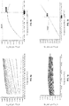
FIGs. 2 and 3 , the results of 3000 random simulation runs of the above described bandgap reference circuit are shown. The simulation has been conducted with

FIGs. 2a and 2b , which illustrate the temperature dependent output voltage VREF, the bandgap reference circuit according to an embodiment of the present application achieves an accuracy of the output voltage VREF better than +/- 2 % without trim (cf.FIG. 2a , where the output voltage VREF varies in the range of approximately 2.5 %) and an accuracy of the output voltage VREF better than +/- 0.5 % in response to a single test insertion at room temperature for absolute trimming. -
FIGs. 3a and 3b illustrate frequency histograms of output voltage VREF determined by the simulation runs shown inFIG. 2a and 2b , respectively, at a temperature of 150°C. Without trim as shown inFIG. 3a , the mean output voltage VREF is 998.5 mV with a standard deviation of 2.8 mV. The maximum output voltage VREF is 1.008 V and the minimum output voltage VREF is 986.7 mV. With a single test insertion trim as shown inFIG. 3b , the mean output voltage VREF is 998.7 mV with a standard deviation of 877 µV. The maximum output voltage VREF is 1.002 V and the minimum output voltage VREF is 995.9 mV. - Referring first back to
FIG. 1 , the properties and characteristics of the current IBIP, which flows from theemitter junction node 250 to ground, should be further discussed for a fuller understanding of the operation of the bandgap reference circuit according to an embodiment of the present application. The bipolar current IBIP is dependent on the emitter voltage Vemitter at theemitter junction node 250. The emitter voltage Vemitter is equal to
- Hence, the emitter voltage Vemitter has a (strong) positive temperature dependency.
FIG. 4a schematically shows a diagram of the emitter voltage Vemitter over temperature illustrating the variation of the emitter voltage Vemitter.FIG. 4b schematically shows a diagram of the bipolar current IBIP flowing fromemitter junction node 250 to ground, the bias current IBIAS flowing through thebias resistor R 5 270 and the current ICTAT flowing throughresistor R 4 350, wherein


- The variation range of the temperature dependent emitter voltage Vemitter produces a corresponding variation range of the bias current IBIAS. In order to mitigate the strong positive temperature dependency of the bias current IBIAS, the
bias resistor R 5 270 may be selected with appropriate temperature coefficient(s). The temperature dependent resistance of thebias resistor R 5 270 may be modelled as following:
- Next, the temperature dependency or curvature of the emitter voltage VBE should be considered. Note that the aforementioned relationship applies to the bipolar current IBIP, the bias current IBIAS and the emitter current ICTAT:

- The emitter voltage VBE as a function of temperature is approximated as following:

- To determine appropriate temperature coefficients tc1 and tc2, the above discussed
bandgap reference circuit 100 is modified by replacing thebias resistor R 5 270 with a current supply (or sink) 270' having optimized properties.FIG. 5 illustrates a modified bandgap reference circuit 100' with current supply according to an example of the present application. The remaining components correspond to those in thebandgap reference circuit 100 described above with reference toFIGs. 1 to 4 . - The current supply 270' supplying a nominal current of 3 µA and having a temperature dependency equal to that of the above described model of the
bias resistor R 5 270 with temperature coefficients tc1 and tc2. The temperature coefficients tc1 and tc2 may be varied for analysis. For instance, the temperature coefficients tc1 may be varied in a range between -3·10-3 °C-1 and +5·10-3 °C-1. The temperature coefficients tc2 may be varied in a range between -5·10-6 °C-2 and +15·10-6 °C-2. - In a first step, the temperature coefficients tc2 is set to 0 °C-2 to study the effect of varying the temperature coefficient tc1 in the range from -3·10-3 °C-1 to +5·10-3 °C-1. The current of the current supply 270' is set to 3 µA.
FIG. 6a schematically illustrates the second derivative of the output voltage VREF over the temperature in the range from -40°C to 120°C.FIG. 6b schematically illustrates the second derivative of the output voltage VREF at room temperature (approx. 27°C) as the temperature coefficient tc1 varies over the range from -3·10-3 °C-1 to +5·10-3 °C-1. The second derivative of the output voltage VREF has a local maximum at tc1 ≈ 3·10-3 °C-1 within the range of variation. - In a next step, the temperature coefficient tc1 is set to 3·10-3 °C-1 to study the effect of varying the temperature coefficient tc2 in the range from -5·10-6 °C-2 to +15·10-6 °C-2. The current of the current supply 270' is again set to 3 µA.
FIG. 7a schematically illustrates the second derivative of the output voltage VREF over the temperature in the range from -40°C to 120°C.FIG. 7b schematically illustrates the second derivative of the output voltage VREF at room temperature (approx. 27°C) over the temperature coefficient tc2 varied over the range from -5·10-6 °C-2 to + 15·10-6 °C-2. The second derivative of the output voltage VREF changes its sign at the temperature coefficient tc2 approximately tc2 ≈ 7·10-6 °C-2. The second derivative of the output voltage VREF being smaller than 0 (being negative) means that the curvature is negative whereas the second derivative of the output voltage VREF being greater than 0 (being positive) means that the curvature is positive. - The above determined temperature coefficients tc1 and tc2 may be considered as best fit temperature coefficients to optimize or minimize the curvature of the output voltage VREF.
- Referring to
FIG. 8 , a diagram of the output voltage VREF of the modified bandgap reference circuit 100' with two different parameter sets for the current supply 270' over the temperature range from -40°C to 150°C is schematically illustrated. - In general, the current supply 270' provides a temperature dependent current, which is modeled as following:

- The upper profile of the output voltage VREF is determined based on lo = 3 µA, tc1 = 3·10-3 °C-1 and tc2 = 7·10-6 °C-2. The lower profile of the output voltage VREF is determined based on lo = 3 µA, tc1 = 3·10-3 °C-1 and tc2 = 6·10-6 °C-2. The obtained curvatures are significantly lower, which is immediately understood when comprising the profiles shown in
FIGs. 8 and2 . - The above discussion of the modified bandgap reference circuit 100' enables those skilled in the art to implement a
bias resistor R 5 270 with an appropriate temperature dependency in order to improve the curvature of the output voltage VREF of thebandgap reference circuit 100. The technology, which is used to implement thebandgap reference circuit 100 may limit the choice of implementation possibilities of thebias resistor R 5 270. An approach to minimize the curvature of the output voltage VREF of thebandgap reference circuit 100 will be described with reference toFIG. 9 . - A feasible approach to minimize the curvature of the output voltage VREF of the
bandgap reference circuit 100 is to select abias resistor R 5 270 with a temperature coefficient tc2, which is the quadratic temperature coefficient tc2, as close as possible to the above discussed best fit temperature coefficient tc2 ≈ 7·10-6 °C-2. For instance, thebias resistor R 5 270 may be implemented as polysilicon resistor with a quadratic temperature coefficient tc2 ≈ 10·10-6 °C-2, thereby accepting a negative linear temperature coefficient tc1, which causes an increase of the bias current through thebias resistor R 5 270. - Referring now to
FIG. 9 , a schematic circuit diagram of abandgap reference circuit 105 according to another embodiment of the present application is shown, which comprises acurvature compensation stage 400, which consumes a current from the bipolar current IBIP thereby reducing the bias current through thebias resistor R 5 270. Those skilled in the art will immediately understand that thebandgap reference circuit 105 described in the following corresponds to thebandgap reference circuit 100 described above but is supplemented with thecurvature compensation stage 400. Hence, the above description with reference to thebandgap reference circuit 100 applies likewise to thebandgap reference circuit 105 described herein. The following description should be read in the context with the above description. It should be noted that the above introduced base-emitter current ICTAT will be referred to a first base-emitter current ICTAT1 in the following. - The
curvature compensation stage 400 is also supplied by the current supply. In particular, thecurrent mirror circuitry 115 provides a current IS3 a respective output. Thecurrent mirror circuitry 115 supplies the same current Is at the outputs, e.g. Is = IS1 = IS2 = IS3. In an example, thecurrent mirror circuitry 115 further comprises atransistor 410 providing the source current signals IS3 at one of its current terminals, whereas the other one of its current terminals is coupled to thesupply voltage rail 110. In particular, the control terminal of thetransistor 410 is connected to the current terminal of thetransistor 120 providing the source current signal Isi and further to the control terminals of thetransistors - In an example, the
transistor 410 is a MOSFET (metal-oxide-semiconductor field-effect transistor). In particular, thetransistor 410 is p-channel MOSFET. The source terminal of thetransistor 410 is connected to thesupply voltage rail 110. The drain terminal of thetransistor 410 supplies the source current signal IS3. The gate terminal of thetransistor 410 is connected to the drain terminal of thetransistor 120 and to the gate terminals of thetransistors - The current supply supplies the source current signal IS3 to a further branch comprising a bipolar junction transistor (BJT) 420. In particular, the
BJT 420 is a pnp-type bipolar transistor. A first current terminal of theBJT 420 is connected to the respective output of thecurrent mirror circuitry 115. In an example, the emitter terminal of theBJT 420 is connected to the current supply and the collector terminal of theBJT 420 is connected to ground, e.g. theground rail 150. - A
resistor R 6 430 is connected between to the first current terminal of theBJT 420 the control terminal of theBJT 420. In particular, theresistor R 6 430 is connected between the emitter terminal and the base terminal of theBJT 420. Hence, a base-emitter voltage VBE of theBJT 420 occurs across theresistor R 6 430, which causes a compensation current ICTAT2 to flow through theresistor R 6 430. - A further
current mirror circuitry 445 is connected between the control terminal of theBJT 420 and ground. Thecurrent mirror circuitry 445 accepts the compensation current ICTAT2 flowing through theresistor R 6 430 and consumes an equivalent compensation current ICTAT2 from the base-emitter current ICTAT1. For instance, thecurrent mirror circuitry 445 has a first input to accept the compensation current ICTAT2 and a second input to consume the equivalent compensation current ICTAT2 from the base-emitter current ICTAT1. The first input is connected to anode 425 between control terminal of theBJT 420 and theresistor R 6 430 and the second input is connected to anode 460 between theresistor R 4 350 and thebias resistor R 5 270. - Hence, the bias current IBIAS is reduced by the equivalent compensation current ICTAT2:


- The
current mirror circuitry 445 comprises inparticular transistors transistor 450 is connected to the current terminal of thetransistor 440 accepting the compensation current ICTAT2 and is further connected to the control terminal of thetransistor 440. - In an example, the
transistors transistors transistors ground rail 150. The drain terminal of thetransistor 440 is connected to thenode 425, which is connected in series between theresistor R 6 430 and the base terminal of theBJT 420 and accepts the compensation current ICTAT2 flowing through theresistor R 6 430. The gate terminal of thetransistor 450 is connected to the drain terminal and to the gate terminal of thetransistor 440. - Referring now to
FIG. 10 , a diagram of the output voltage VREF of the above describedbandgap reference circuit 105 with curvature compensation over the temperature range from -40°C to 150°C is schematically illustrated. The above described curvature compensation enables the curvature to be limited to approximately ± 100 µV. - In an example, a base current compensation for the base currents of the
BJTs bandgap reference circuits BJTs resistor R 3 340 may be connected in series with the base terminal of theBJT 230 and a second compensation resistor having a resistance substantially equal to the resistance of theresistor R 1 310 may be connected in series with the base terminal of theBJT 240. In particular, the first compensation resistor may be connected in series between the base terminal of theBJT 230 and thenode 315 and the second compensation resistor may be connected in series between the base terminal of theBJT 240 and thenode 345. The current gain values β of theBJTs BJTs BJT 230. - The base current compensation is exemplarily illustrated in
FIG. 11 in connection with the above exemplifiedbandgap reference circuit 100 ofFIG. 1 . The base current compensation comprises the firstcompensation resistor R C1 360 and the secondcompensation resistor R C2 370 each connected to a respective one of the base terminals of theBJTs bandgap reference circuit 105 ofFIG. 9 . - According to an example of the present application, a sub-bandgap reference source circuit is provided. The circuit comprises a current mirror source arranged to supply a same current to a first branch comprising a first bipolar junction transistor, BJT, and a second branch comprising a second bipolar junction transistor, BJT. The first BJT has an emitter current density, which is lower than the emitter current density of the second BJT. The first branch and the second branch are connected at a first node, which is coupled to ground. The circuit further comprises a first voltage divider comprising a first resistance and a second resistance coupled in series. The first resistance is coupled between a base terminal of the first BJT and a second node. The second resistor is coupled to ground. The circuit further comprises a second voltage divider comprising a third resistance and a fourth resistance coupled in series. The third resistance is coupled between the second node and a base terminal of the second BJT. The fourth resistance is coupled to the first node. The circuit further comprises an output terminal coupled to the second node.
- According to an example, the first and second BJTs are npn-type bipolar transistors.
- According to an example, the circuit further comprises a supply voltage rail coupled to the current mirror source.
- 4 According to an example, the circuit further comprises a transistor having a first current terminal coupled to the supply voltage rail, a second current terminal coupled to the second node and a control terminal coupled to the second branch.
- According to an example, the first current terminal is a drain terminal and the second current terminal is a source terminal.
- According to an example, the circuit further comprises a bias resistance coupled between the first node and ground.
- According to an example, the first resistance and/or the second resistance of the first voltage divider is a trimmable resistance.
- According to an example, the first resistance and/or the second resistance of the second voltage divider is a trimmable resistance.
- According to an example, the emitter density of the first BJT is of a factor higher than the emitter density of the second BJT. The factor is higher than 1. In an example, the factor is in the range of 8 to 15, in particular the factor is substantially 8.
- According to an example, the current mirror source comprises two transistors. The gate terminals of the two transistors are connected to each other and to a drain terminal of one of the two transistors.
- According to an example, the first BJT has a collector terminal coupled to the current mirror source and an emitter terminal coupled to the first node. The second BJT has a collector terminal coupled to the current mirror source and an emitter terminal coupled to the first node.
- According to an example, the circuit further comprises a third branch supplied by the current mirror source with a second current. The third branch includes a third bipolar junction transistor, BJT, and a resistance coupled between the current mirror source and a base terminal of the third BJT. The circuit further comprises a current mirror coupled between the base terminal of the third BJT and ground. The current mirror is further coupled between the first node and ground.
- According to an example, the same current and the second current has a predetermined fixed ratio. In an example, the second current and the second current have the same value.
- According to an example, the third BJT is a pnp-type bipolar transistor.
- According to an example, the current mirror comprises two transistors. Gate terminals of the two transistors are connected to each other and to a drain terminal of one of the two transistors, which is coupled to the base terminal of the third BJT.
- Those of skill in the art would understand that information and signals may be represented using any of a variety of different technologies and techniques. Those of skill would further appreciate that the various illustrative logical blocks, modules, circuits, and algorithm steps described in connection with the disclosure herein may be implemented as electronic hardware, computer software, or combinations of both. To illustrate clearly this interchangeability of hardware and software, various illustrative components, blocks, modules, circuits, and steps have been described above generally in terms of their functionality. Whether such functionality is implemented as hardware or software depends upon the particular application and design constraints imposed on the overall system. Skilled artisans may implement the described functionality in varying ways for each particular application, but such implementation decisions should not be interpreted as causing a departure from the scope of the present disclosure.
- The previous description of the disclosure is provided to enable any person skilled in the art to make or use the disclosure. Various modifications to the disclosure will be readily apparent to those skilled in the art, and the generic principles defined herein may be applied to other variations without departing from the spirit or scope of the disclosure. Thus, the disclosure is not intended to be limited to the examples and designs described herein but is to be accorded the widest scope consistent with the principles and novel features disclosed herein.
Claims (15)
- A sub-bandgap reference source circuit, comprising:a current mirror source (115) arranged to supply a same current (IS1, IS2) toa first branch comprising a first bipolar junction transistor, BJT, (230) and a second branch comprising a second bipolar junction transistor, BJT, (240),wherein the first BJT (230) has an emitter current density, which is lower than the emitter current density of the second BJT (240),wherein the first branch and the second branch are connected at a first node (250), which is coupled to ground,a first voltage divider comprising a first resistance (R1, 310) and a second resistance (R2, 320) coupled in series, wherein the first resistance (320) is coupled between a base terminal of the first BJT (230) and a second node (330), wherein the second resistor (320) is coupled to ground;a second voltage divider comprising a third resistance (R3, 340) and a fourth resistance (R4, 350) coupled in series, wherein the third resistance (R3, 340) is coupled between the second node (330) and a base terminal of the second BJT (240), wherein the fourth resistance (R4, 350) is coupled to the first node (250); andan output terminal (170) coupled to the second node (330).
- The sub-bandgap reference source circuit according to claim 1, wherein the first and second BJTs (230, 240) are npn-type bipolar transistors.
- The sub-bandgap reference source circuit according to claim 1 or claim 2, further comprising:
a supply voltage rail (110) coupled to the current mirror source (115). - The sub-bandgap reference source circuit according to claim 3, further comprising:
a transistor (140) having a first current terminal coupled to the supply voltage rail (110), a second current terminal coupled to the second node (330) and a control terminal coupled to the second branch. - The sub-bandgap reference source circuit according to claim 4, wherein the first current terminal is a drain terminal and the second current terminal is a source terminal.
- The sub-bandgap reference source circuit according to any preceding claim, further comprising:
a bias resistance (270) coupled between the first node (250) and ground. - The sub-bandgap reference source circuit according to any preceding claim,
wherein at least one of the first resistance (310) and the second resistance (320) of the first voltage divider is a trimmable resistance. - The sub-bandgap reference source circuit according to any preceding claim,
wherein at least one of the first resistance (340) and the second resistance (350) of the second voltage divider is a trimmable resistance. - The sub-bandgap reference source circuit according to any preceding claim, wherein the emitter density of the first BJT is higher than the emitter density of the second BJT (240) by a factor higher than 1.
- The sub-bandgap reference source circuit according to any preceding claim, wherein the current mirror source (115) comprises two transistors (120, 130), wherein gate terminals of the two transistors (120, 130) are connected to each other and to a drain terminal of one of the two transistors (120, 130).
- The sub-bandgap reference source circuit according to any preceding claim,
wherein the first BJT (230) has a collector terminal coupled to the current mirror source (115) and an emitter terminal coupled to the first node (250),
wherein the second BJT (240) has a collector terminal coupled to the current mirror source (115) and an emitter terminal coupled to the first node (250). - The sub-bandgap reference source circuit according to any preceding claim, further comprising a third branch supplied by the current mirror source (115) with the a second current (IS3), wherein the third branch includes:a third bipolar junction transistor, BJT, (420) and a resistance (430) coupled between the current mirror source (115) and a base terminal; anda current mirror (445) coupled between the base terminal of the third BJT (420) and ground, wherein the current mirror is further coupled between the first node (250) and ground.
- The sub-bandgap reference source circuit according to claim 12, wherein the same current (IS1, IS2) and the second current (IS3) have a predetermined fixed ratio.
- The sub-bandgap reference source circuit according to claim 11 or claim 12, wherein the third BJT (420) is a pnp-type bipolar transistor.
- The sub-bandgap reference source circuit according to any one of the claims 11 to 14,
wherein the current mirror (445) comprises two transistors (440, 450), wherein gate terminals of the two transistors (440, 450) are connected to each other and to a drain terminal of one of the two transistors (440, 450), which is coupled to the base terminal of the third BJT (420).
Priority Applications (2)
| Application Number | Priority Date | Filing Date | Title |
|---|---|---|---|
| EP18306711.5A EP3671400B1 (en) | 2018-12-18 | 2018-12-18 | Sub-bandgap reference voltage source |
| US16/701,393 US10712763B2 (en) | 2018-12-18 | 2019-12-03 | Sub-bandgap reference voltage source |
Applications Claiming Priority (1)
| Application Number | Priority Date | Filing Date | Title |
|---|---|---|---|
| EP18306711.5A EP3671400B1 (en) | 2018-12-18 | 2018-12-18 | Sub-bandgap reference voltage source |
Publications (2)
| Publication Number | Publication Date |
|---|---|
| EP3671400A1 true EP3671400A1 (en) | 2020-06-24 |
| EP3671400B1 EP3671400B1 (en) | 2022-05-11 |
Family
ID=65278134
Family Applications (1)
| Application Number | Title | Priority Date | Filing Date |
|---|---|---|---|
| EP18306711.5A Active EP3671400B1 (en) | 2018-12-18 | 2018-12-18 | Sub-bandgap reference voltage source |
Country Status (2)
| Country | Link |
|---|---|
| US (1) | US10712763B2 (en) |
| EP (1) | EP3671400B1 (en) |
Families Citing this family (9)
| Publication number | Priority date | Publication date | Assignee | Title |
|---|---|---|---|---|
| EP3812873B1 (en) * | 2019-10-24 | 2025-02-26 | NXP USA, Inc. | Voltage reference generation with compensation for temperature variation |
| TWI736350B (en) * | 2020-07-07 | 2021-08-11 | 瑞昱半導體股份有限公司 | Voltage reduction circuit for bandgap reference voltage circuit |
| CN112130615B (en) * | 2020-11-25 | 2021-03-12 | 上海芯龙半导体技术股份有限公司 | Reference source circuit and chip |
| US11449088B2 (en) | 2021-02-10 | 2022-09-20 | Nxp B.V. | Bandgap reference voltage generator with feedback circuitry |
| US12164323B2 (en) * | 2021-06-07 | 2024-12-10 | Texas Instruments Incorporated | Temperature drift correction in a voltage reference |
| KR20240122115A (en) | 2023-02-03 | 2024-08-12 | 삼성전자주식회사 | Clock signal generator and its operating method |
| US20240402737A1 (en) * | 2023-05-30 | 2024-12-05 | Texas Instruments Incorporated | Reference circuit |
| US12366872B2 (en) * | 2023-08-30 | 2025-07-22 | Nexperia B.V. | Electronic device with reduced process spread bandgap |
| US12111675B1 (en) * | 2024-04-09 | 2024-10-08 | Itu472, Llc | Curvature-corrected bandgap reference |
Citations (3)
| Publication number | Priority date | Publication date | Assignee | Title |
|---|---|---|---|---|
| US4282477A (en) * | 1980-02-11 | 1981-08-04 | Rca Corporation | Series voltage regulators for developing temperature-compensated voltages |
| US20090302823A1 (en) * | 2008-06-10 | 2009-12-10 | Analog Devices, Inc. | Voltage regulator circuit |
| US9110485B2 (en) * | 2007-09-21 | 2015-08-18 | Freescale Semiconductor, Inc. | Band-gap voltage reference circuit having multiple branches |
Family Cites Families (3)
| Publication number | Priority date | Publication date | Assignee | Title |
|---|---|---|---|---|
| US6630859B1 (en) * | 2002-01-24 | 2003-10-07 | Taiwan Semiconductor Manufacturing Company | Low voltage supply band gap circuit at low power process |
| US6661713B1 (en) * | 2002-07-25 | 2003-12-09 | Taiwan Semiconductor Manufacturing Company | Bandgap reference circuit |
| US8400213B2 (en) | 2008-11-18 | 2013-03-19 | Freescale Semiconductor, Inc. | Complementary band-gap voltage reference circuit |
-
2018
- 2018-12-18 EP EP18306711.5A patent/EP3671400B1/en active Active
-
2019
- 2019-12-03 US US16/701,393 patent/US10712763B2/en active Active
Patent Citations (3)
| Publication number | Priority date | Publication date | Assignee | Title |
|---|---|---|---|---|
| US4282477A (en) * | 1980-02-11 | 1981-08-04 | Rca Corporation | Series voltage regulators for developing temperature-compensated voltages |
| US9110485B2 (en) * | 2007-09-21 | 2015-08-18 | Freescale Semiconductor, Inc. | Band-gap voltage reference circuit having multiple branches |
| US20090302823A1 (en) * | 2008-06-10 | 2009-12-10 | Analog Devices, Inc. | Voltage regulator circuit |
Also Published As
| Publication number | Publication date |
|---|---|
| US20200192414A1 (en) | 2020-06-18 |
| EP3671400B1 (en) | 2022-05-11 |
| US10712763B2 (en) | 2020-07-14 |
Similar Documents
| Publication | Publication Date | Title |
|---|---|---|
| EP3671400B1 (en) | Sub-bandgap reference voltage source | |
| US7710096B2 (en) | Reference circuit | |
| US7495505B2 (en) | Low supply voltage band-gap reference circuit and negative temperature coefficient current generation unit thereof and method for supplying band-gap reference current | |
| US6507180B2 (en) | Bandgap reference circuit with reduced output error | |
| US8159206B2 (en) | Voltage reference circuit based on 3-transistor bandgap cell | |
| US7078958B2 (en) | CMOS bandgap reference with low voltage operation | |
| TWI282050B (en) | A proportional to absolute temperature voltage circuit | |
| US8063623B2 (en) | Analog compensation circuit | |
| US7902912B2 (en) | Bias current generator | |
| US20170115677A1 (en) | Low noise reference voltage generator and load regulator | |
| CN102369495A (en) | Method and circuit for low power voltage reference and bias current generator | |
| EP3926437B1 (en) | A high accuracy zener based voltage reference circuit | |
| EP3929694B1 (en) | A voltage regulator | |
| CN103792980A (en) | Reference voltage generation circuit | |
| US6759893B2 (en) | Temperature-compensated current source | |
| CN101180594A (en) | Process-invariant bandgap reference circuit and method | |
| US20130069616A1 (en) | Offset calibration technique to improve performance of band-gap voltage reference | |
| CN115525090A (en) | Method, system and apparatus for generating a compensated voltage reference | |
| US7629785B1 (en) | Circuit and method supporting a one-volt bandgap architecture | |
| US12282350B2 (en) | Bandgap circuit with noise reduction and temperature stability | |
| US9304528B2 (en) | Reference voltage generator with op-amp buffer | |
| EP4460737A1 (en) | Reference voltage generator based on threshold voltage difference of field effect transistors | |
| US9618952B2 (en) | Current generator circuit and method of calibration thereof | |
| EP3244281B1 (en) | An on chip temperature independent current generator | |
| US20100171547A1 (en) | Pseudo bandgap voltage reference circuit |
Legal Events
| Date | Code | Title | Description |
|---|---|---|---|
| PUAI | Public reference made under article 153(3) epc to a published international application that has entered the european phase |
Free format text: ORIGINAL CODE: 0009012 |
|
| STAA | Information on the status of an ep patent application or granted ep patent |
Free format text: STATUS: THE APPLICATION HAS BEEN PUBLISHED |
|
| AK | Designated contracting states |
Kind code of ref document: A1 Designated state(s): AL AT BE BG CH CY CZ DE DK EE ES FI FR GB GR HR HU IE IS IT LI LT LU LV MC MK MT NL NO PL PT RO RS SE SI SK SM TR |
|
| AX | Request for extension of the european patent |
Extension state: BA ME |
|
| STAA | Information on the status of an ep patent application or granted ep patent |
Free format text: STATUS: REQUEST FOR EXAMINATION WAS MADE |
|
| 17P | Request for examination filed |
Effective date: 20210111 |
|
| RBV | Designated contracting states (corrected) |
Designated state(s): AL AT BE BG CH CY CZ DE DK EE ES FI FR GB GR HR HU IE IS IT LI LT LU LV MC MK MT NL NO PL PT RO RS SE SI SK SM TR |
|
| GRAP | Despatch of communication of intention to grant a patent |
Free format text: ORIGINAL CODE: EPIDOSNIGR1 |
|
| STAA | Information on the status of an ep patent application or granted ep patent |
Free format text: STATUS: GRANT OF PATENT IS INTENDED |
|
| INTG | Intention to grant announced |
Effective date: 20220124 |
|
| GRAS | Grant fee paid |
Free format text: ORIGINAL CODE: EPIDOSNIGR3 |
|
| GRAA | (expected) grant |
Free format text: ORIGINAL CODE: 0009210 |
|
| STAA | Information on the status of an ep patent application or granted ep patent |
Free format text: STATUS: THE PATENT HAS BEEN GRANTED |
|
| AK | Designated contracting states |
Kind code of ref document: B1 Designated state(s): AL AT BE BG CH CY CZ DE DK EE ES FI FR GB GR HR HU IE IS IT LI LT LU LV MC MK MT NL NO PL PT RO RS SE SI SK SM TR |
|
| REG | Reference to a national code |
Ref country code: GB Ref legal event code: FG4D |
|
| REG | Reference to a national code |
Ref country code: CH Ref legal event code: EP |
|
| REG | Reference to a national code |
Ref country code: AT Ref legal event code: REF Ref document number: 1491985 Country of ref document: AT Kind code of ref document: T Effective date: 20220515 |
|
| REG | Reference to a national code |
Ref country code: DE Ref legal event code: R096 Ref document number: 602018035367 Country of ref document: DE |
|
| REG | Reference to a national code |
Ref country code: IE Ref legal event code: FG4D |
|
| REG | Reference to a national code |
Ref country code: LT Ref legal event code: MG9D |
|
| REG | Reference to a national code |
Ref country code: NL Ref legal event code: MP Effective date: 20220511 |
|
| REG | Reference to a national code |
Ref country code: AT Ref legal event code: MK05 Ref document number: 1491985 Country of ref document: AT Kind code of ref document: T Effective date: 20220511 |
|
| PG25 | Lapsed in a contracting state [announced via postgrant information from national office to epo] |
Ref country code: SE Free format text: LAPSE BECAUSE OF FAILURE TO SUBMIT A TRANSLATION OF THE DESCRIPTION OR TO PAY THE FEE WITHIN THE PRESCRIBED TIME-LIMIT Effective date: 20220511 Ref country code: PT Free format text: LAPSE BECAUSE OF FAILURE TO SUBMIT A TRANSLATION OF THE DESCRIPTION OR TO PAY THE FEE WITHIN THE PRESCRIBED TIME-LIMIT Effective date: 20220912 Ref country code: NO Free format text: LAPSE BECAUSE OF FAILURE TO SUBMIT A TRANSLATION OF THE DESCRIPTION OR TO PAY THE FEE WITHIN THE PRESCRIBED TIME-LIMIT Effective date: 20220811 Ref country code: NL Free format text: LAPSE BECAUSE OF FAILURE TO SUBMIT A TRANSLATION OF THE DESCRIPTION OR TO PAY THE FEE WITHIN THE PRESCRIBED TIME-LIMIT Effective date: 20220511 Ref country code: LT Free format text: LAPSE BECAUSE OF FAILURE TO SUBMIT A TRANSLATION OF THE DESCRIPTION OR TO PAY THE FEE WITHIN THE PRESCRIBED TIME-LIMIT Effective date: 20220511 Ref country code: HR Free format text: LAPSE BECAUSE OF FAILURE TO SUBMIT A TRANSLATION OF THE DESCRIPTION OR TO PAY THE FEE WITHIN THE PRESCRIBED TIME-LIMIT Effective date: 20220511 Ref country code: GR Free format text: LAPSE BECAUSE OF FAILURE TO SUBMIT A TRANSLATION OF THE DESCRIPTION OR TO PAY THE FEE WITHIN THE PRESCRIBED TIME-LIMIT Effective date: 20220812 Ref country code: FI Free format text: LAPSE BECAUSE OF FAILURE TO SUBMIT A TRANSLATION OF THE DESCRIPTION OR TO PAY THE FEE WITHIN THE PRESCRIBED TIME-LIMIT Effective date: 20220511 Ref country code: ES Free format text: LAPSE BECAUSE OF FAILURE TO SUBMIT A TRANSLATION OF THE DESCRIPTION OR TO PAY THE FEE WITHIN THE PRESCRIBED TIME-LIMIT Effective date: 20220511 Ref country code: BG Free format text: LAPSE BECAUSE OF FAILURE TO SUBMIT A TRANSLATION OF THE DESCRIPTION OR TO PAY THE FEE WITHIN THE PRESCRIBED TIME-LIMIT Effective date: 20220811 Ref country code: AT Free format text: LAPSE BECAUSE OF FAILURE TO SUBMIT A TRANSLATION OF THE DESCRIPTION OR TO PAY THE FEE WITHIN THE PRESCRIBED TIME-LIMIT Effective date: 20220511 |
|
| PG25 | Lapsed in a contracting state [announced via postgrant information from national office to epo] |
Ref country code: RS Free format text: LAPSE BECAUSE OF FAILURE TO SUBMIT A TRANSLATION OF THE DESCRIPTION OR TO PAY THE FEE WITHIN THE PRESCRIBED TIME-LIMIT Effective date: 20220511 Ref country code: PL Free format text: LAPSE BECAUSE OF FAILURE TO SUBMIT A TRANSLATION OF THE DESCRIPTION OR TO PAY THE FEE WITHIN THE PRESCRIBED TIME-LIMIT Effective date: 20220511 Ref country code: LV Free format text: LAPSE BECAUSE OF FAILURE TO SUBMIT A TRANSLATION OF THE DESCRIPTION OR TO PAY THE FEE WITHIN THE PRESCRIBED TIME-LIMIT Effective date: 20220511 Ref country code: IS Free format text: LAPSE BECAUSE OF FAILURE TO SUBMIT A TRANSLATION OF THE DESCRIPTION OR TO PAY THE FEE WITHIN THE PRESCRIBED TIME-LIMIT Effective date: 20220911 |
|
| PG25 | Lapsed in a contracting state [announced via postgrant information from national office to epo] |
Ref country code: SM Free format text: LAPSE BECAUSE OF FAILURE TO SUBMIT A TRANSLATION OF THE DESCRIPTION OR TO PAY THE FEE WITHIN THE PRESCRIBED TIME-LIMIT Effective date: 20220511 Ref country code: SK Free format text: LAPSE BECAUSE OF FAILURE TO SUBMIT A TRANSLATION OF THE DESCRIPTION OR TO PAY THE FEE WITHIN THE PRESCRIBED TIME-LIMIT Effective date: 20220511 Ref country code: RO Free format text: LAPSE BECAUSE OF FAILURE TO SUBMIT A TRANSLATION OF THE DESCRIPTION OR TO PAY THE FEE WITHIN THE PRESCRIBED TIME-LIMIT Effective date: 20220511 Ref country code: EE Free format text: LAPSE BECAUSE OF FAILURE TO SUBMIT A TRANSLATION OF THE DESCRIPTION OR TO PAY THE FEE WITHIN THE PRESCRIBED TIME-LIMIT Effective date: 20220511 Ref country code: DK Free format text: LAPSE BECAUSE OF FAILURE TO SUBMIT A TRANSLATION OF THE DESCRIPTION OR TO PAY THE FEE WITHIN THE PRESCRIBED TIME-LIMIT Effective date: 20220511 Ref country code: CZ Free format text: LAPSE BECAUSE OF FAILURE TO SUBMIT A TRANSLATION OF THE DESCRIPTION OR TO PAY THE FEE WITHIN THE PRESCRIBED TIME-LIMIT Effective date: 20220511 |
|
| REG | Reference to a national code |
Ref country code: DE Ref legal event code: R097 Ref document number: 602018035367 Country of ref document: DE |
|
| PLBE | No opposition filed within time limit |
Free format text: ORIGINAL CODE: 0009261 |
|
| STAA | Information on the status of an ep patent application or granted ep patent |
Free format text: STATUS: NO OPPOSITION FILED WITHIN TIME LIMIT |
|
| PG25 | Lapsed in a contracting state [announced via postgrant information from national office to epo] |
Ref country code: AL Free format text: LAPSE BECAUSE OF FAILURE TO SUBMIT A TRANSLATION OF THE DESCRIPTION OR TO PAY THE FEE WITHIN THE PRESCRIBED TIME-LIMIT Effective date: 20220511 |
|
| 26N | No opposition filed |
Effective date: 20230214 |
|
| PG25 | Lapsed in a contracting state [announced via postgrant information from national office to epo] |
Ref country code: SI Free format text: LAPSE BECAUSE OF FAILURE TO SUBMIT A TRANSLATION OF THE DESCRIPTION OR TO PAY THE FEE WITHIN THE PRESCRIBED TIME-LIMIT Effective date: 20220511 |
|
| REG | Reference to a national code |
Ref country code: CH Ref legal event code: PL |
|
| REG | Reference to a national code |
Ref country code: BE Ref legal event code: MM Effective date: 20221231 |
|
| P01 | Opt-out of the competence of the unified patent court (upc) registered |
Effective date: 20230725 |
|
| PG25 | Lapsed in a contracting state [announced via postgrant information from national office to epo] |
Ref country code: LU Free format text: LAPSE BECAUSE OF NON-PAYMENT OF DUE FEES Effective date: 20221218 |
|
| PG25 | Lapsed in a contracting state [announced via postgrant information from national office to epo] |
Ref country code: LI Free format text: LAPSE BECAUSE OF NON-PAYMENT OF DUE FEES Effective date: 20221231 Ref country code: IE Free format text: LAPSE BECAUSE OF NON-PAYMENT OF DUE FEES Effective date: 20221218 Ref country code: CH Free format text: LAPSE BECAUSE OF NON-PAYMENT OF DUE FEES Effective date: 20221231 |
|
| PG25 | Lapsed in a contracting state [announced via postgrant information from national office to epo] |
Ref country code: BE Free format text: LAPSE BECAUSE OF NON-PAYMENT OF DUE FEES Effective date: 20221231 |
|
| PG25 | Lapsed in a contracting state [announced via postgrant information from national office to epo] |
Ref country code: IT Free format text: LAPSE BECAUSE OF FAILURE TO SUBMIT A TRANSLATION OF THE DESCRIPTION OR TO PAY THE FEE WITHIN THE PRESCRIBED TIME-LIMIT Effective date: 20220511 |
|
| PG25 | Lapsed in a contracting state [announced via postgrant information from national office to epo] |
Ref country code: HU Free format text: LAPSE BECAUSE OF FAILURE TO SUBMIT A TRANSLATION OF THE DESCRIPTION OR TO PAY THE FEE WITHIN THE PRESCRIBED TIME-LIMIT; INVALID AB INITIO Effective date: 20181218 |
|
| PG25 | Lapsed in a contracting state [announced via postgrant information from national office to epo] |
Ref country code: CY Free format text: LAPSE BECAUSE OF FAILURE TO SUBMIT A TRANSLATION OF THE DESCRIPTION OR TO PAY THE FEE WITHIN THE PRESCRIBED TIME-LIMIT Effective date: 20220511 |
|
| PG25 | Lapsed in a contracting state [announced via postgrant information from national office to epo] |
Ref country code: MK Free format text: LAPSE BECAUSE OF FAILURE TO SUBMIT A TRANSLATION OF THE DESCRIPTION OR TO PAY THE FEE WITHIN THE PRESCRIBED TIME-LIMIT Effective date: 20220511 |
|
| PG25 | Lapsed in a contracting state [announced via postgrant information from national office to epo] |
Ref country code: MC Free format text: LAPSE BECAUSE OF FAILURE TO SUBMIT A TRANSLATION OF THE DESCRIPTION OR TO PAY THE FEE WITHIN THE PRESCRIBED TIME-LIMIT Effective date: 20220511 |
|
| PG25 | Lapsed in a contracting state [announced via postgrant information from national office to epo] |
Ref country code: TR Free format text: LAPSE BECAUSE OF FAILURE TO SUBMIT A TRANSLATION OF THE DESCRIPTION OR TO PAY THE FEE WITHIN THE PRESCRIBED TIME-LIMIT Effective date: 20220511 Ref country code: MC Free format text: LAPSE BECAUSE OF FAILURE TO SUBMIT A TRANSLATION OF THE DESCRIPTION OR TO PAY THE FEE WITHIN THE PRESCRIBED TIME-LIMIT Effective date: 20220511 |
|
| PG25 | Lapsed in a contracting state [announced via postgrant information from national office to epo] |
Ref country code: MT Free format text: LAPSE BECAUSE OF FAILURE TO SUBMIT A TRANSLATION OF THE DESCRIPTION OR TO PAY THE FEE WITHIN THE PRESCRIBED TIME-LIMIT Effective date: 20220511 |
|
| PG25 | Lapsed in a contracting state [announced via postgrant information from national office to epo] |
Ref country code: BG Free format text: LAPSE BECAUSE OF FAILURE TO SUBMIT A TRANSLATION OF THE DESCRIPTION OR TO PAY THE FEE WITHIN THE PRESCRIBED TIME-LIMIT Effective date: 20220511 |
|
| PG25 | Lapsed in a contracting state [announced via postgrant information from national office to epo] |
Ref country code: BG Free format text: LAPSE BECAUSE OF FAILURE TO SUBMIT A TRANSLATION OF THE DESCRIPTION OR TO PAY THE FEE WITHIN THE PRESCRIBED TIME-LIMIT Effective date: 20220511 |
|
| PGFP | Annual fee paid to national office [announced via postgrant information from national office to epo] |
Ref country code: DE Payment date: 20251126 Year of fee payment: 8 |
|
| PGFP | Annual fee paid to national office [announced via postgrant information from national office to epo] |
Ref country code: GB Payment date: 20251119 Year of fee payment: 8 |
|
| PGFP | Annual fee paid to national office [announced via postgrant information from national office to epo] |
Ref country code: FR Payment date: 20251120 Year of fee payment: 8 |