EP3667819A1 - Antenna device - Google Patents
Antenna device Download PDFInfo
- Publication number
- EP3667819A1 EP3667819A1 EP18843211.6A EP18843211A EP3667819A1 EP 3667819 A1 EP3667819 A1 EP 3667819A1 EP 18843211 A EP18843211 A EP 18843211A EP 3667819 A1 EP3667819 A1 EP 3667819A1
- Authority
- EP
- European Patent Office
- Prior art keywords
- slit
- antenna
- linear element
- board
- crossing portion
- Prior art date
- Legal status (The legal status is an assumption and is not a legal conclusion. Google has not performed a legal analysis and makes no representation as to the accuracy of the status listed.)
- Withdrawn
Links
Images




Classifications
-
- H—ELECTRICITY
- H01—ELECTRIC ELEMENTS
- H01Q—ANTENNAS, i.e. RADIO AERIALS
- H01Q1/00—Details of, or arrangements associated with, antennas
- H01Q1/27—Adaptation for use in or on movable bodies
- H01Q1/32—Adaptation for use in or on road or rail vehicles
- H01Q1/325—Adaptation for use in or on road or rail vehicles characterised by the location of the antenna on the vehicle
- H01Q1/3275—Adaptation for use in or on road or rail vehicles characterised by the location of the antenna on the vehicle mounted on a horizontal surface of the vehicle, e.g. on roof, hood, trunk
-
- H—ELECTRICITY
- H01—ELECTRIC ELEMENTS
- H01Q—ANTENNAS, i.e. RADIO AERIALS
- H01Q1/00—Details of, or arrangements associated with, antennas
- H01Q1/36—Structural form of radiating elements, e.g. cone, spiral, umbrella; Particular materials used therewith
- H01Q1/38—Structural form of radiating elements, e.g. cone, spiral, umbrella; Particular materials used therewith formed by a conductive layer on an insulating support
-
- H—ELECTRICITY
- H01—ELECTRIC ELEMENTS
- H01Q—ANTENNAS, i.e. RADIO AERIALS
- H01Q1/00—Details of, or arrangements associated with, antennas
- H01Q1/52—Means for reducing coupling between antennas; Means for reducing coupling between an antenna and another structure
- H01Q1/521—Means for reducing coupling between antennas; Means for reducing coupling between an antenna and another structure reducing the coupling between adjacent antennas
-
- H—ELECTRICITY
- H01—ELECTRIC ELEMENTS
- H01Q—ANTENNAS, i.e. RADIO AERIALS
- H01Q13/00—Waveguide horns or mouths; Slot antennas; Leaky-waveguide antennas; Equivalent structures causing radiation along the transmission path of a guided wave
- H01Q13/10—Resonant slot antennas
-
- H—ELECTRICITY
- H01—ELECTRIC ELEMENTS
- H01Q—ANTENNAS, i.e. RADIO AERIALS
- H01Q21/00—Antenna arrays or systems
- H01Q21/28—Combinations of substantially independent non-interacting antenna units or systems
-
- H—ELECTRICITY
- H01—ELECTRIC ELEMENTS
- H01Q—ANTENNAS, i.e. RADIO AERIALS
- H01Q5/00—Arrangements for simultaneous operation of antennas on two or more different wavebands, e.g. dual-band or multi-band arrangements
- H01Q5/40—Imbricated or interleaved structures; Combined or electromagnetically coupled arrangements, e.g. comprising two or more non-connected fed radiating elements
-
- H—ELECTRICITY
- H01—ELECTRIC ELEMENTS
- H01Q—ANTENNAS, i.e. RADIO AERIALS
- H01Q9/00—Electrically-short antennas having dimensions not more than twice the operating wavelength and consisting of conductive active radiating elements
- H01Q9/04—Resonant antennas
- H01Q9/30—Resonant antennas with feed to end of elongated active element, e.g. unipole
-
- H—ELECTRICITY
- H01—ELECTRIC ELEMENTS
- H01Q—ANTENNAS, i.e. RADIO AERIALS
- H01Q9/00—Electrically-short antennas having dimensions not more than twice the operating wavelength and consisting of conductive active radiating elements
- H01Q9/04—Resonant antennas
- H01Q9/30—Resonant antennas with feed to end of elongated active element, e.g. unipole
- H01Q9/32—Vertical arrangement of element
-
- H—ELECTRICITY
- H01—ELECTRIC ELEMENTS
- H01Q—ANTENNAS, i.e. RADIO AERIALS
- H01Q9/00—Electrically-short antennas having dimensions not more than twice the operating wavelength and consisting of conductive active radiating elements
- H01Q9/04—Resonant antennas
- H01Q9/30—Resonant antennas with feed to end of elongated active element, e.g. unipole
- H01Q9/40—Element having extended radiating surface
-
- H—ELECTRICITY
- H01—ELECTRIC ELEMENTS
- H01Q—ANTENNAS, i.e. RADIO AERIALS
- H01Q9/00—Electrically-short antennas having dimensions not more than twice the operating wavelength and consisting of conductive active radiating elements
- H01Q9/04—Resonant antennas
- H01Q9/30—Resonant antennas with feed to end of elongated active element, e.g. unipole
- H01Q9/42—Resonant antennas with feed to end of elongated active element, e.g. unipole with folded element, the folded parts being spaced apart a small fraction of the operating wavelength
-
- H—ELECTRICITY
- H04—ELECTRIC COMMUNICATION TECHNIQUE
- H04W—WIRELESS COMMUNICATION NETWORKS
- H04W4/00—Services specially adapted for wireless communication networks; Facilities therefor
- H04W4/30—Services specially adapted for particular environments, situations or purposes
- H04W4/40—Services specially adapted for particular environments, situations or purposes for vehicles, e.g. vehicle-to-pedestrians [V2P]
Definitions
- the present invention relates to an antenna device that is installed in a vehicle and used for V2X (Vehicle-to-X, Vehicle-to-Everything) communication (e.g., a vehicle-to-vehicle communication and a road-to-vehicle communication), etc..
- V2X Vehicle-to-X, Vehicle-to-Everything
- the present invention relates to a vehicular antenna device that includes an antenna board in which a slit antenna is provided.
- Conventional antennas of the above kind includes a dipole antenna that is pattern-printed on a board as a V2X communication antenna.
- a conductor transmission line is necessary to feed power to the dipole antenna.
- a dipole antenna that is installed vertically has a problem that its radiation pattern is prone to be distorted due to the presence of the transmission line to deteriorate its performance because an antenna element and the transmission line tend to be arranged parallel with each other. This means a disadvantage that it is difficult to design the antenna device including the transmission line so as to avoid deterioration of the performance of the dipole antenna.
- the slit antenna includes a parasitic slit that does not overlap with the linear element when the first surface and the second surface are superimposed on each other.
- the antenna device further includes a capacitance loading element, wherein the antenna board be spaced from the capacitance loading element in a front-rear direction of the antenna board.
- the linear element is provided on the first surface of the dielectric substrate
- the slit antenna is provided on the second surface opposite to the first surface of the dielectric substrate
- the linear element and the slit antenna coupled to each other such that the linear element and a slit or slits of the slit antenna overlap with each other when the first surface and the second surface are superimposed on each other.
- the slit antenna can operate without providing a transmission line on the second surface of the dielectric substrate and the antenna device can be designed easily because the slit antenna involves the linear element.
- the filter 45 exhibits a low impedance in an AM/FM broadcast frequency band and a high impedance in respective operation frequency bands of the GNSS antenna 2 and the antenna board 5. That is, in the AM/FM broadcast frequency band, the divisional bodies 41, 42, 43, and 44 can be regarded as being connected to each other to form a single large conductor.
- the top end of a coil 32 is connected to the capacitance loading element 31 and the bottom end of the coil 32 is connected to the circuit board 10.
- a first conductor pattern 71 is provided as the linear element 50 on the left side surface of the dielectric substrate 11.
- the linear element 50 has a common linear element portion 51, a first branch linear element portion 52, and a second branch linear element portion 53.
- the common linear element portion 51 is wider than the first branch linear element portion 52 and the second branch linear element portion 53.
- a bottom end portion of the common linear element portion 51 reaches the bottom edge of the dielectric substrate 11 and serves as a first feeding end portion 60 that is a feeding point for feeding a signal in the 5.9-GHz band for V2X communication.
- the first feeding end portion 60 is located at a position that is lower than the radiation electrode surface of the GNSS antenna 2.
- Fig. 7 is an explanatory diagram that is a superimposition of the left side view ( Fig. 5 ) and the right side view ( Fig. 6 ) of the antenna board 5.
- the first branch linear element portion 52 crosses (overlaps with) the first slit 55 at a first crossing portion 58 by getting across the first slit 55 from below to above.
- the second branch linear element portion 53 crosses (overlaps with) the second slit 57 at a second crossing portion 59 by getting across the second slit 57 from above to below.
- the length of a portion of the second branch linear element portion 53 from the point where it branches off the common linear element portion 51 to the second crossing portion 59 is shorter than the length of a portion of the first branch linear element portion 52 from the point where it branches off the common linear element portion 51 to the first crossing portion 58 by ⁇ /2.
- This setting is made for a reason that since the first branch linear element portion 52 gets across the first slit 55 from below to above and the second branch linear element portion 53 gets across the second slit 57 from above to below, to render the first slit 55 and the second slit 57 in phase it is necessary to make the first crossing portion 58 and the second crossing portion 59 in opposite phase.
- the linear element 50 does not cross the parasitic slit 56.
- the average gain in an azimuth angle range 90° to 270° is 2.7 dBi.
- the bandpass filter 80 a signal in a V2X communication frequency band in which the antenna board 5 operates as a slit antenna flows to the ground via the bandpass filter 80.
- the average gain of the slit antenna 54 of the first embodiment in the azimuth angle range 90° to 270° is larger than in the case without the bandpass filter 80.
- the length of the first branch linear element portion 52 from the point where it branches off the common linear element portion 51 to the first crossing portion 58 is set equal to the length of the second branch linear element portion 53 from the point where it branches off the common linear element portion 51 to the second crossing point 59.
- the other part of the configuration is the same in the above-described first embodiment.
- the fourth embodiment is different from the above-described first embodiment in that a capacitance loading element 31A of the AM/FM broadcast reception antenna 3 is an umbrella-shaped conductor plate and has a structure which is not divided.
- the capacitance loading element 31A extends alongside and is fixed to a holder 93 which is erected from and fixed to the base 90.
- a coil 32 is attached to the holder 93, the top end of the coil 32 is connected to the capacitance loading element 31A, and the bottom end of the capacitance loading element 31A is connected to an amplifier board 94 which is fixed to the case 90.
- the interval between the first slit 55 and the second slit 57 is ⁇ /2, it may be longer than ⁇ /2.
- the distance from the first feed end portion 60 of the linear element 50 to the second crossing portion 59 may be set shorter than the distance from the first feed end portion 60 to the first crossing portion 58 by an integer (larger than or equal to 1) multiple of ⁇ .
- both of a linear element and a slit antenna may be provided on one surface of the dielectric substrate. In this case, no conductor pattern is provided around the linear element 50.
Landscapes
- Engineering & Computer Science (AREA)
- Remote Sensing (AREA)
- Physics & Mathematics (AREA)
- Electromagnetism (AREA)
- Waveguide Aerials (AREA)
- Details Of Aerials (AREA)
- Variable-Direction Aerials And Aerial Arrays (AREA)
Abstract
Description
- The present invention relates to an antenna device that is installed in a vehicle and used for V2X (Vehicle-to-X, Vehicle-to-Everything) communication (e.g., a vehicle-to-vehicle communication and a road-to-vehicle communication), etc.. In particular, the present invention relates to a vehicular antenna device that includes an antenna board in which a slit antenna is provided.
- Conventional antennas of the above kind includes a dipole antenna that is pattern-printed on a board as a V2X communication antenna. However, a conductor transmission line is necessary to feed power to the dipole antenna. In particular, a dipole antenna that is installed vertically has a problem that its radiation pattern is prone to be distorted due to the presence of the transmission line to deteriorate its performance because an antenna element and the transmission line tend to be arranged parallel with each other. This means a disadvantage that it is difficult to design the antenna device including the transmission line so as to avoid deterioration of the performance of the dipole antenna.
- Patent document 1:
JP-A-6-188610
Patent document 1 is an example in which a dipole antenna is provided on a printed board. - The present invention has been made with recognition of the above circumstances, and an object of the invention is therefore to provide an antenna device that can be designed easily.
- One aspect of the present invention is an antenna device. This antenna device includes an antenna board in which a conductor pattern is provided on each of both surfaces of a dielectric substrate, wherein a linear element is provided on a first surface of the dielectric substrate, a slit antenna is provided on a second surface of the dielectric substrate opposite to the first surface, and when the first surface and the second surface are superimposed on each other, the linear element and a slit of the slit antenna overlap with each other.
- It is preferable that the slit includes plural slits.
- It is preferable that the slit antenna includes a parasitic slit that does not overlap with the linear element when the first surface and the second surface are superimposed on each other.
- It is preferable that the antenna board is erected perpendicular to and fixed to an attachment member, that the slit antenna includes a first slit that overlaps with the linear element at a first crossing portion and a second slit that overlaps with the linear element at a second crossing portion when the first surface and the second surface are superimposed on each other, and that a distance from a feeding point, located on a side of the attachment member, of the linear element to the second crossing portion is shorter than a distance from the feeding point to the first crossing portion.
- It is preferable that the slit antenna includes a first slit that overlaps with the linear element at a first crossing portion and a second slit that overlaps with the linear element at a second crossing portion when the first surface and the second surface are superimposed on each other, that a direction in which the linear element gets across the first slit is the same as a direction in which the linear element gets across the second slit, and that a distance from a feeding point of the linear element to the second crossing portion is equal to a distance from the feeding point to the first crossing portion.
- It is preferable that when the first surface and the second surface are superimposed on each other, a direction in which the linear element gets across the first slit is opposite to a direction in which the linear element gets across the second slit, and that the distance from the feeding point of the linear element to the second crossing portion is shorter than the distance from the feeding point to the first crossing portion by an odd number multiple of λ/2, where the odd number is larger than or equal to 1 and λ is an effective wavelength of an operation frequency of the slit antenna.
- It is preferable that when the first surface and the second surface are superimposed on each other, a direction in which the linear element gets across the first slit is the same as a direction in which the linear element gets across the second slit, and that the distance from the feeding point of the linear element to the second crossing portion is shorter by an integer multiple of λ, where the integer is larger than or equal to 1 and λ is an effective wavelength of an operation frequency of the slit antenna.
- It is preferable that the antenna board operates at a frequency that is different from an operation frequency of the slit antenna.
- It is preferable that the antenna device further includes a capacitance loading element, wherein the antenna board be spaced from the capacitance loading element in a front-rear direction of the antenna board.
- Any combinations of the above constituent elements and what are obtained by converting expressions of the invention between methods, systems, etc. are also effective embodiments of the invention.
- In the antenna device according to the invention, the linear element is provided on the first surface of the dielectric substrate, the slit antenna is provided on the second surface opposite to the first surface of the dielectric substrate, and the linear element and the slit antenna coupled to each other such that the linear element and a slit or slits of the slit antenna overlap with each other when the first surface and the second surface are superimposed on each other. As a result, the slit antenna can operate without providing a transmission line on the second surface of the dielectric substrate and the antenna device can be designed easily because the slit antenna involves the linear element.
-
- [
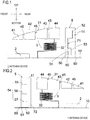
Fig. 1] Fig. 1 is a left side view, with its head located on the front side, of an antenna device according to a first embodiment of the present invention (a case is omitted). - [
Fig. 2] Fig. 2 is a right side view, with its head located on the front side, of the same (the case is omitted). - [
Fig. 3] Fig. 3 is a rear view of the same with the case omitted. - [
Fig. 4] Fig. 4 is a plan view of the same with the case omitted. - [
Fig. 5] Fig. 5 is a left side view, with its head located on the front side, of an antenna board employed in the first embodiment in which a slit antenna is provided. - [
Fig. 6] Fig. 6 is a right side view, with its head located on the front side, of the same antenna board. - [
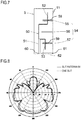
Fig. 7] Fig. 7 is an explanatory diagram that is a superimposition of the left side view (Fig. 5 ) and the right side view (Fig. 6 ) of the antenna board. - [
Fig. 8] Fig. 8 is a directivity characteristic diagram, produced by simulations, showing horizontal plane directivity characteristics (a slit antenna elevation angle: 0°) of the antenna board employed in the first embodiment and an antenna board in which a slit antenna having only one slit is formed. - [
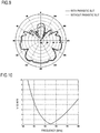
Fig. 9] Fig. 9 is a directivity characteristic diagram, produced by simulations, showing horizontal plane directivity characteristics (the slit antenna elevation angle: 0°) of the antenna board employed in the first embodiment and an antenna board in which a parasitic slit is not provided. - [
Fig. 10] Fig. 10 is a VSWR characteristic diagram of the antenna board employed in the first embodiment in a case that a feeding end portion (a feeding point) is different from the slit antenna - [
Fig. 11] Fig. 11 is a directivity characteristic diagram, produced by simulations, showing horizontal plane directivity characteristics (an elevation angle: 0°) of the antenna board employed in the first embodiment in a case that a bandpass filter that makes the voltage of the feeding end portion that is different from the slit antenna equal to the ground (GND) level at an operation frequency of the slit antenna is provided and a case that the bandpass filter is not provided. - [
Fig. 12] Fig. 12 is an explanatory diagram showing anantenna board 5A employed in the second embodiment and is a superimposition of a left side view and a right side view of the antenna board - [
Fig. 13] Fig. 13 is a directivity characteristic diagram, produced by simulations, showing horizontal plane directivity characteristics (the elevation angle: 0°) at a frequency 5,887.5 MHz of theantenna board 5 employed in the first embodiment and theantenna board 5A employed in the second embodiment. - [
Fig. 14] Fig. 14 is a left side view, with its head located on the front side, of an antenna board employed in a third embodiment in which a slit antenna is provided. - [
Fig. 15] Fig. 15 is a right side view, with its head located on the front side, of the same. - [
Fig. 16] Fig. 16 is an explanatory diagram that is a superimposition of the left side view (Fig. 14 ) and the right side view (Fig. 15 ) of the antenna board. - [
Fig. 17] Fig. 17 is a frequency characteristic diagram showing how the axial ratio of a GNSS antenna varies with the division number of a capacitance loading element. - [
Fig. 18] Fig. 18 is a frequency characteristic diagram showing how the average gain of the GNSS antenna varies with the division number of the capacitance loading element. - [
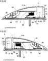
Fig. 19] Fig. 19 is a left side view, with its head located on the front side, of a vehicular antenna device according to a fourth embodiment of the invention. - [
Fig. 20] Fig. 20 is a right side view, with its head located on the front side, of the same. - Preferred embodiments of the present invention will be hereinafter described in detail with reference to the drawings. The same or equivalent constituent elements, members, treatment/working processes, or the like shown in the drawings are given the same symbol and redundant descriptions therefor will be avoided as appropriate. The embodiments are just examples and are not intended to restrict the invention; it is not always the case that all of features described in the embodiments or combinations of those features are essential to the invention.
- An antenna device according to a first embodiment of the invention will be described with reference to
Figs. 1-7 . As shown in these drawings, in theantenna device 1, a GNSS antenna (a patch antenna) 2, an AM/FMbroadcast reception antenna 3, and anantenna board 5 in which a V2X communication slit antenna is provided are installed on acircuit board 10 which is fixed to an antenna base (not shown), so as to be arranged in this order from the front side. Thecircuit board 10 has attachment members for fixing theGNSS antenna 2, the AM/FMbroadcast reception antenna 3, and theantenna board 5. These constituent elements are housed in an internal space that is surrounded by the antenna base and a radio wave transmissive case (a radome) which covers the antenna base from above. TheGNSS antenna 2, which is equipped with a radiation electrode provided on a top surface and has upward directivity, is fixed to thecircuit board 10 via an attachment member. TheGNSS antenna 2 may be fixed to a circuit board that is different from thecircuit board 10. As shown inFig. 1 , the front side and the rear side of theantenna device 1 are defined as the destination sides of the leftward direction and the rightward direction on the paper surface, respectively, and the top side and the bottom side of theantenna device 1 are defined as the destination sides of the upward direction and the downward direction on the paper surface, respectively. The following description will be made according to these definitions. - The AM/FM
broadcast reception antenna 3 has acapacitance loading element 31 and acoil 31 which is directly connected to thecapacitance loading element 31. Thecapacitance loading element 31 is supported by support means on the antenna base. As shown inFigs. 3 and 4 , thecapacitance loading element 31 has no top portion and is configured such that bottom edges of divisional bodies opposed to each other in the left-right direction are connected to each other and it is divided in the front-rear direction. That is, thecapacitance loading element 31 is configured such that adjacent ones ofdivisional bodies filter 45. Thefilter 45 exhibits a low impedance in an AM/FM broadcast frequency band and a high impedance in respective operation frequency bands of theGNSS antenna 2 and theantenna board 5. That is, in the AM/FM broadcast frequency band, thedivisional bodies coil 32 is connected to thecapacitance loading element 31 and the bottom end of thecoil 32 is connected to thecircuit board 10. - In the first embodiment, although the
GNSS antenna 2 is disposed under thecapacitance loading element 31, influence of thecapacitance loading element 31 is alleviated because thecapacitance loading element 31 is divided.Fig. 17 shows a relationship between the division number of the capacitance loading element and the axial ratio of theGNSS antenna 2. Although the axial ratio is not good when the capacitance loading element is not divided (i.e., the capacitance loading element is a single, large-area conductor plate), the axial ratio becomes smaller and better as the division number is increased in order of two, three, and four (corresponding to thecapacitance loading element 31 of the first embodiment).Fig. 18 shows a relationship between the division number of the capacitance loading element and the average gain of theGNSS antenna 2. The average gain is small when the capacitance loading element is not divided, and the average gain increases as the division number is increased in order of three and four (corresponding to thecapacitance loading element 31 of the first embodiment). - The
antenna board 5 having the V2Xcommunication slit antenna 54 is fixed to an attachment member of thecircuit board 10 so as to be erected from the attachment member perpendicularly. As shown inFigs. 5-7 , in theantenna board 5, alinear element 50 and theslit antenna 54 which is coupled to thelinear element 50 are constructed by a conductor pattern provided on each of both surfaces of adielectric substrate 11 by printing of the conductor pattern, etching of a conductor foil, or the like. Theslit antenna 54 has a configuration that it has a slit which is open at only one end and is surrounded by a conductor except the one end and the slit is fed with power. That is, theslit antenna 54 has a slit which one end is open and the other end is closed. On the other hand, slot antennas are known that are similar in configuration to theslit antenna 54 but operate differently than it. Slot antennas have a configuration that a slot is surrounded fully by a conductor and fed with power. That is, slot antennas have a slot that is closed at both ends. - In this example, a
first conductor pattern 71 is provided as thelinear element 50 on the left side surface of thedielectric substrate 11. Thelinear element 50 has a commonlinear element portion 51, a first branchlinear element portion 52, and a second branchlinear element portion 53. The commonlinear element portion 51 is wider than the first branchlinear element portion 52 and the second branchlinear element portion 53. A bottom end portion of the commonlinear element portion 51 reaches the bottom edge of thedielectric substrate 11 and serves as a firstfeeding end portion 60 that is a feeding point for feeding a signal in the 5.9-GHz band for V2X communication. As seen fromFigs. 1 and 2 , the firstfeeding end portion 60 is located at a position that is lower than the radiation electrode surface of theGNSS antenna 2. - A
second conductor pattern 72 is provided on the almost entire surface of the right side surface of thedielectric substrate 11 shown inFig. 6 , and theslit antenna 54 is portions where thesecond conductor pattern 72 is not provided, that is, afirst slit 55, aparasitic slit 56, and asecond slit 57. The length of each of thefirst slit 55, theparasitic slit 56, and thesecond slit 57 is λ/4, where λ is an effective wavelength at a V2X communication operation frequency (5.9-GHz band) on thedielectric substrate 11. The interval between thefirst slit 55 and theparasitic slit 56 in the height direction of thedielectric substrate 11 is λ/4, and the interval between theparasitic slit 56 and thesecond slit 57 in the height direction of thedielectric substrate 11 is also λ/4. Thus, the distance between thefirst slit 55 and thesecond slit 57 is λ/2. - The
antenna board 5 operates as a monopole antenna at frequencies in the 925-MHz band which is used in remote control systems (e.g., Keyless Entry Systems, Remote Start Systems, and Bi-directional Remote Engine Starters) in addition to frequencies in the 5.9-GHz band which is used for V2X communication. Let λk represent an effective wavelength at a frequency in the 925-MHz band on thedielectric substrate 11 ; then the height of theantenna board 5 is set at λk/4. A secondfeeding end portion 61 which is a feeding point for allowing theantenna board 5 to serve as a monopole antenna is provided at a bottom end portion of thesecond conductor pattern 72. To form the secondfeeding end portion 61 at a rear end portion of the bottom edge of thedielectric substrate 11, aconductor-less portion 62 where no part of the conductor pattern is provided is provided so as to extend along the bottom edge of thedielectric substrate 11. -
Fig. 7 is an explanatory diagram that is a superimposition of the left side view (Fig. 5 ) and the right side view (Fig. 6 ) of theantenna board 5. The first branchlinear element portion 52 crosses (overlaps with) thefirst slit 55 at afirst crossing portion 58 by getting across thefirst slit 55 from below to above. The second branchlinear element portion 53 crosses (overlaps with) thesecond slit 57 at asecond crossing portion 59 by getting across thesecond slit 57 from above to below. The length of a tip portion, going upward from thefirst crossing portion 58, of the first branch linear element portion 52 (i.e., an end portion opposite to the position where the first branchlinear element portion 52 branches off the common linear element portion 51) is λ/4. The length of a tip portion, going downward from thesecond crossing portion 59, of the second branch linear element portion 53 (i.e., an end portion opposite to the position where the second branchlinear element portion 53 branches off the common linear element portion 51) is λ/4. The length of a portion of the second branchlinear element portion 53 from the point where it branches off the commonlinear element portion 51 to thesecond crossing portion 59 is shorter than the length of a portion of the first branchlinear element portion 52 from the point where it branches off the commonlinear element portion 51 to thefirst crossing portion 58 by λ/2. This setting is made for a reason that since the first branchlinear element portion 52 gets across thefirst slit 55 from below to above and the second branchlinear element portion 53 gets across thesecond slit 57 from above to below, to render thefirst slit 55 and thesecond slit 57 in phase it is necessary to make thefirst crossing portion 58 and thesecond crossing portion 59 in opposite phase. As seen fromFig. 7 , thelinear element 50 does not cross theparasitic slit 56. - Where the
antenna board 5 is used as theslit antenna 54 for V2X communication, a signal in the 5.9-GHz band is supplied to the firstfeeding end portion 60 which is the bottom end portion of the commonlinear element portion 51 via thecircuit board 10. Where theantenna board 5 is used in a remote control system, a signal in the 925-MHz band is supplied using the secondfeeding end portion 61 which is the bottom end portion of thesecond conductor pattern 72 on the right side surface of thedielectric substrate 11. Thus, the secondfeeding end portion 61 which is the bottom end portion of thesecond conductor pattern 72 cannot be directly connected the ground (GND) of thecircuit board 10, in other words, the ground of the antenna base (not shown). Thus, as shown inFigs. 1 and 2 , abandpass filter 80 is mounted on thecircuit board 10 in the vicinity of a portion to which the secondfeeding end portion 61 is connected. Thebandpass filter 80 keeps the secondfeeding end portion 61 in a high-impedance state with respect to the ground for a signal in the 925-MHz band for a remote control system, and exhibits a low impedance to make the voltage of the secondfeeding end portion 61 substantially equal to the ground level in the 5.9-GHz band (at an operation frequency of the slit antenna 54) for V2X communication . One end of thebandpass filter 80 is connected to the secondfeeding end portion 61 and the other end of thebandpass filter 80 is grounded via the circuit board 10 (i.e., connected to the ground). -
Fig. 8 is a directivity characteristic diagram, produced by simulations, showing horizontal plane directivity characteristics (the elevation angle: 0°) at a frequency 5,887.5 MHz of theantenna board 5 employed in the first embodiment and an antenna board in which a slit antenna having only one slit is formed. The characteristic of theantenna board 5 is represented by a solid line inFig. 8 and the characteristic of the antenna board in which the slit antenna having only one slit is formed is represented by a dotted line inFig. 8 . The horizontal plane corresponds to theelevation angle 0° and the rear direction of theantenna device 1 corresponds to theazimuth angle 180°. The average gain of theslit antenna 54 which is provided in theantenna board 5 in an azimuth angle range 90° to 270° (the elevation angle: 0°) is 3.7 dBi, and the average gain of the slit antenna having only one slit in anazimuth anglerange 90° to 270° (the elevation angle: 0°) is 2.0 dBi. As shown inFig. 8 , the average gain in the azimuth angle range 90° to 270° (the elevation angle: 0°) of theslit antenna 54 is larger than that of the slit antenna having only one slit. -
Fig. 9 is a directivity characteristic diagram, produced by simulations, showing horizontal plane directivity characteristics (the elevation angle: 0°) at a frequency 5,887.5 MHz of theantenna board 5 employed in the first embodiment and an antenna board without a parasitic slit. The characteristic of theantenna board 5 is represented by a solid line inFig. 9 and the characteristic of the antenna board without a parasitic slit is represented by a dotted line inFig. 9 . The average gain of theantenna board 5 with theparasitic slit 56 in an azimuth angle range 90° to 270° (the elevation angle: 0°) is 3.7 dBi, and the average gain of the antenna board without a parasitic slit in an azimuth angle range 90° to 270° (the elevation angle: 0°) is 2.7 dBi. Where theparasitic slit 56 is provided, the coupling between thefirst slit 55 and thesecond slit 57 is weakened. As shown inFig. 9 , the average gain in the azimuth angle range 90° to 270° (the elevation angle: 0°) of theslit antenna 54 with theparasitic slit 56 is larger than that of the slit antenna without theparasitic slit 56. -
Fig. 10 is a VSWR characteristic diagram of theantenna board 5 employed in the first embodiment in a case that the feeding end portion is different from theslit antenna 54, that is, the secondfeeding end portion 61 is used. As shown inFig. 10 , theantenna board 5 operates even at frequencies of the 925-MHz band (VSWR is close to 1 in the 925-MHz band). It is therefore unnecessary to provide an antenna for a remote control system separately and hence theantenna device 1 can be miniaturized. -
Fig. 11 is a directivity characteristic diagram, produced by simulations, showing horizontal plane directivity characteristics (the elevation angle: 0°) at a frequency 5,887.5 MHz of theantenna board 5 employed in the first embodiment in a case that thebandpass filter 80 that makes the voltage of the secondfeeding end portion 61 that is different from theslit antenna 54 equal to the ground level at an operation frequency of theslit antenna 54 is provided and a case that thebandpass filter 80 is not provided. Where thebandpass filter 80 is provided (a solid line inFig. 11 ), the average gain in an azimuth angle range 90° to 270° (the elevation angle: 0°) is 3.7 dBi. Where thebandpass filter 80 is not provided (a dotted line inFig. 11 ), the average gain in an azimuth angle range 90° to 270° (the elevation angle: 0°) is 2.7 dBi. Where thebandpass filter 80 is provided, a signal in a V2X communication frequency band in which theantenna board 5 operates as a slit antenna flows to the ground via thebandpass filter 80. By virtue of the use of thebandpass filter 80, the average gain of theslit antenna 54 of the first embodiment in the azimuth angle range 90° to 270° (the elevation angle: 0°) is larger than in the case without thebandpass filter 80. - This embodiment provides the following advantages:
- (1) The
antenna board 5 is configured such that thelinear element 50 is provided on a first surface of thedielectric substrate 11, theslit antenna 54 is provided on a second surface that is opposite to the first surface, and thelinear element 50 overlaps with theslits slit antenna 54 when the first surface and the second surface are superimposed on each other. As a result, it is possible to cause the slit antenna to operate without the need for providing a transmission line on the second surface of thedielectric substrate 11 and a structure is obtained that thelinear element 50 is involved in the slit antenna. Thelinear element 50 can be designed more easily than the transmission line of dipole antenna and theantenna device 1 can be designed more easily than an antenna device that is equipped with a dipole antenna. - (2) Since the
slit antenna 54 has two slits, that is, thefirst slit 55 and thesecond slit 58, which are spaced from each other by λ/2, the average gain in an azimuth angle range 90° to 270° (the elevation angle: 0°) can be made larger than in a slit antenna having only one slit. - (3) In the
slit antenna 54, the coupling between thefirst slit 55 and thesecond slit 57 can be made weaker because theparasitic slit 55 is provided between thefirst slit 55 and thesecond slit 57. The average gain in an azimuth angle range 90° to 270° (the elevation angle: 0°) can be made larger than in a slit antenna without theparasitic slit 55. Theparasitic slit 55 need not always be provided at the center between thefirst slit 55 and thesecond slit 57 in the height direction; it suffices that theparasitic slit 56 be provided between thefirst slit 55 and thesecond slit 57. - (4) The first
feeding end portion 60 which is the point for feeding power from thecircuit board 10 to thelinear element 50 is located on the bottom edge of theantenna board 5. Thefirst slit 55 is located over thesecond slit 57, and in theantenna board 5 the length of the second branch linear element portion 53fromthe point where it branches off the commonlinear element portion 51 to thesecond crossing point 59 is set shorter than the length of the first branchlinear element portion 52 from the point where it branches off the commonlinear element portion 51 to thefirst crossing point 58. With this measure, the layout of thelinear element 50 can be made simpler than in a case that the length of the first branchlinear element portion 52 from the point where it branches off the commonlinear element portion 51 to thefirst crossing point 58 is equal to the length of the second branchlinear element portion 53 from the point where it branches off the commonlinear element portion 51 to the second crossing point 59 (e.g., second embodiment shown inFig. 12 ). - (5) The first branch
linear element portion 52 gets across thefirst slit 55 from below to above and the second branchlinear element portion 53 gets across thesecond slit 57 from above to below. As a result, the length of the second branchlinear element portion 53 from the point where it branches off the commonlinear element portion 51 to thesecond crossing point 59 is set shorter than the length of the first branchlinear element portion 52 from the point where it branches off the commonlinear element portion 51 to thefirst crossing point 58 by λ/2 (this is to make the phase at thefirst crossing point 58 opposite to the phase at the second crossing point 59). With this measure, the average gain in an azimuth angle range 90° to 270° (the elevation angle: 0°) can be made larger than in a case that the length of the first branchlinear element portion 52 from the point where the first branchlinear element portion 52 branches off the commonlinear element portion 51 to thefirst crossing point 58 is equal to the length of the second branchlinear element portion 53 from the point where it branches off the commonlinear element portion 51 to the second crossing point 59 (e.g., second embodiment shown inFig. 12 ). Furthermore, thelinear element 50 can be shortened, whereby the loss due to thelinear element 50 can be reduced. And theantenna board 5 can be shortened in the front-rear direction, whereby theantenna device 1 can be miniaturized. - (6) The
antenna board 5 operates as a monopole antenna not only at frequencies in the 5.9-GHz band that are used for V2X communication but also at frequencies in the 925-MHz band that are used in remote control systems. Thus, it is not necessary to provide an antenna for a remote control system separately, whereby theantenna device 1 can be miniaturized. - (7) The
bandpass filter 80 capable of passing a signal in a frequency band for V2X communication is disposed in the vicinity of the secondfeeding end portion 61, whereby the voltage of the secondfeeding end portion 61 and thesecond conductor pattern 72 can be made substantially equal to the ground level in the 5.9-GHz band in the frequency band for V2X communication. Thus, theantenna board 5 can operate as theslit antenna 54 for V2X communication satisfactorily even in a case that theantenna board 5 is also used as a monopole antenna for a remote control system. - (8) The
antenna board 5 is spaced from thecapacitance loading element 31 of the AM/FMbroadcast reception antenna 3 in the front-rear direction of theantenna board 5. However, since thecapacitance loading element 31 functions as a reflector, the directivity characteristic can be improved on the side where thecapacitance loading element 31 does not exist. -
Fig. 12 is an explanatory diagram showing anantenna board 5A employed in the second embodiment and is a superimposition of a left side view and a right side view of theantenna board 5A. Whereas thesame slit antenna 54 as employed in the first embodiment is employed in the second embodiment, the second embodiment is different from the first embodiment in that the first branchlinear element portion 52 and the second branchlinear element portion 53 cross (overlap with) the firsts slit 55 and thesecond slit 57, respectively, from above to below. To make thefirst slit 55 and thesecond slit 57 in phase, it is necessary to set thefirst crossing portion 58 and thesecond crossing portion 59 in phase. To this end, the length of the first branchlinear element portion 52 from the point where it branches off the commonlinear element portion 51 to thefirst crossing portion 58 is set equal to the length of the second branchlinear element portion 53 from the point where it branches off the commonlinear element portion 51 to thesecond crossing point 59. The other part of the configuration is the same in the above-described first embodiment. -
Fig. 13 is a directivity characteristic diagram, produced by simulations, showing horizontal plane directivity characteristics (an elevation angle of the slit antenna 54: 0°) at a frequency 5,887.5 MHz of theantenna board 5 employed in the first embodiment and theantenna board 5A employed in the second embodiment. In the antenna board shown inFig. 7 , the length of a portion, from the point of branching off the commonlinear element portion 51 to thesecond crossing portion 59, of the second branchlinear element portion 53 is shorter than the length of a portion, from the point of branching off the commonlinear element portion 51 to thefirst crossing portion 58, of the first branchlinear element portion 52 by λ/2. In contrast, in theantenna board 5A shown inFig. 12 , the length of the portion, from the point of branching off the commonlinear element portion 51 to thefirst crossing portion 58, of the first branchlinear element portion 52 is the same as the length of the portion, from the point of branching off the commonlinear element portion 51 to thesecond crossing portion 59, of the second branchlinear element portion 53. - In the characteristic of the
antenna board 5 represented by a solid line inFig. 13 (the length of the portion, from the point of branching off the commonlinear element portion 51 to thesecond crossing portion 59, of the second branchlinear element portion 53 is shorter than the length of the portion, from the point of branching off the commonlinear element portion 51 to thefirst crossing portion 58, of the first branchlinear element portion 52 by λ/2), an average gain in an azimuth angle range 90° to 270° (the elevation angle: 0°) is 3.7 dBi. On the other hand, in the characteristic of theantenna board 5A represented by a dotted line inFig. 13 (the length of the portion, from the point of branching off the commonlinear element portion 51 to thefirst crossing portion 58, of the first branchlinear element portion 52 is equal to the length of the portion, from the point of branching off the commonlinear element portion 51 to thesecond crossing portion 59, of the second branch linear element portion 53), an average gain in an azimuth angle range 90° to 270° (the elevation angle: 0°) is 2.8 dBi. As seen fromFig. 13 , theantenna board 5 employed in the first embodiment in which the second branchlinear element portion 53 is shorter by λ/2 has a larger average gain in the azimuth angle range 90° to 270° (the slit antenna elevation angle: 0°) than theantenna board 5A in the second embodiment in which the second branchlinear element portion 53 has equal length. In this manner, the length of thelinear element 50 of theantenna board 5 is shorter than the length of thelinear element 50 of theantenna board 5A, whereby the loss of thelinear element 50 is reduced and theantenna device 1 can be miniaturized by shortening theantenna board 5 in the front-rear direction (its width direction). That is, an average gain in the azimuth angle range 90° to 270° (the elevation angle: 0°) of theantenna board 5A according to the second embodiment is smaller than in the first embodiment though it is sufficiently larger than an average gain in the remaining azimuth angle range. -
Figs. 14-16 show anantenna board 5B employed in a third embodiment of the present invention. Theantenna board 5B is different from theantenna board 5 employed in the first embodiment in the shapes of the lower slit and the parasitic slit that constitute the slit antenna and the shape of the linear element is different than in theantenna board 5 accordingly. That is, aslit antenna 54A has afirst slit 55, andparasitic slit 56A, and asecond slit 57A, a front end portion of theparasitic slit 56A is bent upward and downward so that theparasitic slit 56A assumes a T-shape, and thesecond slit 57A is bent downward so as to assume an L shape. The sum of the length of theparasitic slit 56A in the front-rear direction and its length in the top-bottom direction is λ/4. The length of thesecond slit 57A including the length of the bent portion is λ/4. The second branchlinear element portion 53 is also bent once additionally so as to be suitable for the shape of thesecond slit 57A. The other part of the configuration is the same as in the first embodiment. - As described above, since the
parasitic slit 56A and thesecond slit 57A are deformed so that their lengths in the front-rear direction are shortened, the length of theantenna board 5B in the front-rear direction can be made shorter than in theantenna board 5. Whereas the length of theantenna board 5 in the front-rear direction is 22 mm, the length of theantenna board 5B in the front-rear direction is 17 mm. - An antenna device according to a fourth embodiment of the invention will be described with reference to
Figs. 19 and 20 . As shown in these drawings, thevehicular antenna device 1A includes ametal base 90 and a radio wave transmissive case (a radome) 92 which is screwed to the base 90 so as to cover the base 90 from above. An SDARS antenna (a patch antenna) 95, an AM/FMbroadcast reception antenna 3, and anantenna board 5 in which a V2X communication slit antenna is provided are installed in an internal space defined by thebase 90 and thecase 92 so as to be arranged in this order from the front side. TheSDARS antenna 95 is equipped with a radiation electrode on a top surface and has upward directivity, and is fixed to thebase 90 via aboard 96. - The fourth embodiment is different from the above-described first embodiment in that a
capacitance loading element 31A of the AM/FMbroadcast reception antenna 3 is an umbrella-shaped conductor plate and has a structure which is not divided. Thecapacitance loading element 31A extends alongside and is fixed to aholder 93 which is erected from and fixed to thebase 90. Acoil 32 is attached to theholder 93, the top end of thecoil 32 is connected to thecapacitance loading element 31A, and the bottom end of thecapacitance loading element 31A is connected to anamplifier board 94 which is fixed to thecase 90. - As shown in
Figs. 17 and 18 , if the patch antenna having the upward directivity is disposed at a low position so as to be covered with thecapacitance loading element 31A having the structure which is not divided, both of the axial ratio and the gain are degraded. Thus, in the fourth embodiment, theSDARS antenna 95 is disposed at a front position so as not to be covered with thecapacitance loading element 31A. In the other part, the configuration and the workings and advantages are the same as in the first embodiment. - Although the invention has been described above using the embodiments as examples, it would be understood by those skilled in the art that the individual constituent elements and treatment/working processes of the embodiments can be modified in various manners within the confines of the claims. Modifications will be described below.
- In the
antenna board 5 employed in the first embodiment, the first branchlinear element portion 52 gets across thefirst slit 55 at thefirst crossing portion 58 from below to above and the second branchlinear element portion 53 gets across thesecond slit 57 at thesecond crossing portion 59 from above to below. However, whether the first branchlinear element portion 52 is to get across thefirst slit 55 at thefirst crossing portion 58 in extending upward or downward and the second branchlinear element portion 53 is to get across thesecond slit 57 at thesecond crossing portion 59 in extending upward or downward can be determined as desired. However, the length of the first branchlinear element portion 52 from the point where it branches off the commonlinear element portion 51 to thefirst crossing portion 58 and the length of the second branchlinear element portion 53 from the point where it branches off the commonlinear element portion 51 to thesecond crossing portion 59 are set so that thefirst slit 55 and thesecond slit 57 are in phase. - Although the
antenna board 5 employed in the first embodiment is configured so as to operate at frequencies in the 925-MHz band for remote control systems in addition to frequencies in a frequency band for V2X communication, it may be configured so as to operate at frequencies in the 700 MHz to 2.7 GHz band for TEL. Theantenna board 5 may be configured so as to operate at frequencies in another band. - Although in the
antenna board 5 employed in the first embodiment the interval between thefirst slit 55 and thesecond slit 57 is λ/2, it may be longer than λ/2. In this case, the distance from the firstfeed end portion 60 of thelinear element 50 to thesecond crossing portion 59 may be set shorter than the distance from the firstfeed end portion 60 to thefirst crossing portion 58 by an odd number (larger than or equal to 1) multiple of λ/2. - Although in the
antenna board 5A employed in the second embodiment the interval between thefirst slit 55 and thesecond slit 57 is λ/2, it may be longer than λ/2. In this case, the distance from the firstfeed end portion 60 of thelinear element 50 to thesecond crossing portion 59 may be set shorter than the distance from the firstfeed end portion 60 to thefirst crossing portion 58 by an integer (larger than or equal to 1) multiple of λ. - Although in the embodiments a rectangular shape, T shape, and an L shape were employed as example slit shapes, the slit shape is not limited to them; for example, a cruciform shape or a rectangle whose corners are rounded may be employed.
- Although in each embodiment the
linear element 50 and theslit antenna linear element 50. - Although in each embodiment the
linear element 50 and theslit antenna linear element 50 is erected from thecircuit board 10 and used as thelinear element 50 and a plate-like thin-plate conductor provided with slits having the same shapes as the slits of theslit antenna slit antenna - Although in the first embodiment the
antenna device 1 is equipped with theGNSS antenna 2, the AM/FMbroadcast reception antenna 3, and theantenna board 5 in which theV2X communication antenna 54 is provided, one or both of theGNSS antenna 2 and the AM/FMbroadcast reception antenna 3 may be omitted if necessary. An antenna having another function may be used in place of theGNSS antenna 2 or the AM/FMbroadcast reception antenna 3. - Although in each embodiment the slit antenna having plural slits is provided in the antenna board, a slit antenna having only one slit that is not a parasitic slit may be provided in the antenna board if no problem arises in the gain of the slit antenna. Furthermore, in each embodiment, a slit antenna having three or more slits that are not a parasitic slit may be provided in the antenna board. Although in each embodiment the slit antenna provided in the antenna board has the parasitic slit, the slit antenna may not include a parasitic slit if no problem arises in the gain of the slit antenna. Although the
bandpass filter 80 is provided in each embodiment, thebandpass filter 80 may be omitted if no problem arises in the gain of the slit antenna. -
- 1, 1A: Vehicular antenna device
- 2: GNSS antenna
- 3: AM/FM broadcast reception antenna
- 5, 5A, 5B: Antenna board
- 10: Circuit board
- 11: Dielectric substrate
- 31: Capacitance loading element
- 32: Coil
- 50: Linear element, 51: Common linear element portion
- 52, 53: Branch linear element portion
- 54, 54A: Slit antenna
- 55, 57, 57A: Slit
- 56, 56A: Parasitic slit
- 58, 59: Crossing portion
- 60, 61: Feeding end potion
- 72: First conductor pattern
- 72: Second conductor pattern
- 80: Lowpass filter
Claims (9)
- An antenna device comprising:an antenna board in which a conductor pattern is provided on each of both surfaces of a dielectric substrate, whereina linear element is provided on a first surface of the dielectric substrate,a slit antenna is provided on a second surface of the dielectric substrate opposite to the first surface, andwhen the first surface and the second surface are superimposed on each other, the linear element and a slit of the slit antenna overlap with each other.
- The antenna device according to claim 1, wherein
the slit includes plural slits. - The antenna device according to claim 1 or 2, wherein
the slit antenna includes a parasitic slit that does not overlap with the linear element when the first surface and the second surface are superimposed on each other. - The antenna device according to any one of claims 1 to 3, wherein
the antenna board is erected perpendicular to and fixed to an attachment member,
the slit antenna has a first slit that overlaps with the linear element at a first crossing portion and a second slit that overlaps with the linear element at a second crossing portion when the first surface and the second surface are superimposed on each other, and
a distance from a feeding point, located on the side of the attachment member, of the linear element to the second crossing portion is shorter than a distance from the feeding point to the first crossing portion. - The antenna device according to any one of claims 1 to 3, wherein
the slit antenna has a first slit that overlaps with the linear element at a first crossing portion and a second slit that overlaps with the linear element at a second crossing portion when the first surface and the second surface are superimposed on each other, and
a direction in which the linear element gets across the first slit is the same as a direction in which the linear element gets across the second slit, and a distance from a feeding point of the linear element to the second crossing portion is equal to a distance from the feeding point to the first crossing portion. - The antenna device according to claim 4, wherein
when the first surface and the second surface are superimposed on each other, a direction in which the linear element gets across the first slit is opposite to a direction in which the linear element gets across the second slit, and
the distance from the feeding point of the linear element to the second crossing portion is shorter than the distance from the feeding point to the first crossing portion by an odd number multiple of λ/2, where the odd number is larger than or equal to 1 and λ is an effective wavelength of an operation frequency of the slit antenna. - The antenna device according to claim 4, wherein
when the first surface and the second surface are superimposed on each other, a direction in which the linear element gets across the first slit is the same as a direction in which the linear element gets across the second slit, and
the distance from the feeding point of the linear element to the second crossing portion is shorter by an integer multiple of λ, where the integer is larger than or equal to 1 and λ is an effective wavelength of an operation frequency of the slit antenna. - The antenna device according to any one of claims 1 to 7, wherein
the antenna board operates at a frequency that is different from an operation frequency of the slit antenna. - The antenna device according to any one of claims 1 to 8, further comprising:a capacitance loading element, whereinthe antenna board is spaced from the capacitance loading element in a front-rear direction of the antenna board.
Applications Claiming Priority (2)
| Application Number | Priority Date | Filing Date | Title |
|---|---|---|---|
| JP2017152359A JP6401835B1 (en) | 2017-08-07 | 2017-08-07 | Antenna device |
| PCT/JP2018/028239 WO2019031270A1 (en) | 2017-08-07 | 2018-07-27 | Antenna device |
Publications (2)
| Publication Number | Publication Date |
|---|---|
| EP3667819A1 true EP3667819A1 (en) | 2020-06-17 |
| EP3667819A4 EP3667819A4 (en) | 2021-05-05 |
Family
ID=63788121
Family Applications (1)
| Application Number | Title | Priority Date | Filing Date |
|---|---|---|---|
| EP18843211.6A Withdrawn EP3667819A4 (en) | 2017-08-07 | 2018-07-27 | ANTENNA DEVICE |
Country Status (5)
| Country | Link |
|---|---|
| US (1) | US11152693B2 (en) |
| EP (1) | EP3667819A4 (en) |
| JP (1) | JP6401835B1 (en) |
| CN (1) | CN110574233B (en) |
| WO (1) | WO2019031270A1 (en) |
Families Citing this family (7)
| Publication number | Priority date | Publication date | Assignee | Title |
|---|---|---|---|---|
| CN113839223B (en) * | 2017-02-23 | 2024-02-27 | 株式会社友华 | Antenna device |
| US11804653B2 (en) * | 2017-02-23 | 2023-10-31 | Yokowo Co., Ltd. | Antenna device having a capacitive loading element |
| JP6956650B2 (en) * | 2018-02-19 | 2021-11-02 | 株式会社ヨコオ | Automotive antenna device |
| CN113782970B (en) * | 2021-09-13 | 2026-02-03 | 立讯精密工业(昆山)有限公司 | Vehicle-mounted antenna assembly and vehicle-mounted antenna device |
| US20240283164A1 (en) * | 2023-02-17 | 2024-08-22 | Commscope Technologies Llc | Radiating elements having dipole arms with cloaked dielectric loading elements and base station antennas including such radiating elements |
| JP7417332B1 (en) * | 2023-05-11 | 2024-01-18 | エイターリンク株式会社 | Multi-antenna and powered device |
| EP4723371A1 (en) * | 2024-10-04 | 2026-04-08 | Valeo Comfort and Driving Assistance | Telematics control unit for a vehicle |
Family Cites Families (29)
| Publication number | Priority date | Publication date | Assignee | Title |
|---|---|---|---|---|
| JPH07118602B2 (en) | 1992-12-18 | 1995-12-18 | 八重洲無線株式会社 | Balun for dipole antenna and printed circuit board |
| JPH0823224A (en) * | 1994-07-11 | 1996-01-23 | N T T Ido Tsushinmo Kk | Notch antenna |
| US5872542A (en) * | 1998-02-13 | 1999-02-16 | Federal Data Corporation | Optically transparent microstrip patch and slot antennas |
| JP3926488B2 (en) * | 1998-09-11 | 2007-06-06 | 日本無線株式会社 | Horizontally polarized horizontal omnidirectional slot antenna |
| US6043785A (en) * | 1998-11-30 | 2000-03-28 | Radio Frequency Systems, Inc. | Broadband fixed-radius slot antenna arrangement |
| WO2001052352A1 (en) * | 2000-01-07 | 2001-07-19 | Modular Mining Systems, Inc. | Array antenna for d-shaped, h-plane radiation pattern |
| JP2002330024A (en) * | 2001-05-01 | 2002-11-15 | Iwatsu Electric Co Ltd | Slot antenna |
| US6879296B2 (en) * | 2001-11-21 | 2005-04-12 | Superpass Company Inc. | Horizontally polarized slot antenna with omni-directional and sectorial radiation patterns |
| FR2853996A1 (en) | 2003-04-15 | 2004-10-22 | Thomson Licensing Sa | Antenna system for PCMCIA card, has transmission antenna placed between two reception antennas, where antenna system is placed at edge of PCMCIA card in zone placed exterior to PCMCIA card reader in computer |
| WO2007058230A1 (en) * | 2005-11-18 | 2007-05-24 | Nec Corporation | Slot antenna and portable wireless terminal |
| CN101401258B (en) * | 2006-05-25 | 2012-10-10 | 松下电器产业株式会社 | Variable slot antenna and method for driving same |
| WO2008065995A1 (en) | 2006-11-30 | 2008-06-05 | Panasonic Corporation | Differential feeding directivity-variable slot antenna |
| JP4904197B2 (en) | 2007-05-08 | 2012-03-28 | パナソニック株式会社 | Unbalanced feed broadband slot antenna |
| JP2011233952A (en) * | 2010-04-23 | 2011-11-17 | Mitsubishi Electric Corp | Housing integrated antenna |
| JP5599098B2 (en) * | 2010-07-30 | 2014-10-01 | 株式会社ヨコオ | Antenna device |
| JP2012054915A (en) * | 2010-08-06 | 2012-03-15 | Nippon Soken Inc | Antenna structure and diversity antenna structure |
| FR2970603A1 (en) * | 2011-01-13 | 2012-07-20 | Thomson Licensing | SLOT TYPE PRINTED DIRECTIVE ANTENNA AND NETWORK SYSTEM MULTIPLE ANTENNAES SLOT-TYPE PRINTED DIRECTIVES |
| EP2495808A1 (en) * | 2011-03-03 | 2012-09-05 | Nxp B.V. | Multiband antenna |
| JP5654917B2 (en) * | 2011-03-24 | 2015-01-14 | 原田工業株式会社 | Antenna device |
| EP2602865B1 (en) * | 2011-12-05 | 2014-10-08 | Nxp B.V. | Multi-band antenna |
| CN104115329B (en) * | 2011-12-14 | 2016-06-29 | 莱尔德技术股份有限公司 | Can by many bands mimo antenna assembly of LTE frequency operation |
| JP2014127751A (en) * | 2012-12-25 | 2014-07-07 | Smart:Kk | Antenna, communication management system and communication system |
| JP2015041994A (en) * | 2013-08-23 | 2015-03-02 | 住友電気工業株式会社 | Slot antenna |
| JP6184802B2 (en) * | 2013-08-26 | 2017-08-23 | 日本ピラー工業株式会社 | Slot antenna |
| DE202014002207U1 (en) | 2014-02-18 | 2014-04-09 | Antennentechnik Abb Bad Blankenburg Gmbh | Multi-range antenna for a receiving and / or transmitting device for mobile use |
| KR20150098343A (en) * | 2014-02-20 | 2015-08-28 | 현대자동차주식회사 | Dual band PCB antenna for vehicle |
| US10103440B2 (en) | 2014-11-06 | 2018-10-16 | Sony Mobile Communications Inc. | Stripline coupled antenna with periodic slots for wireless electronic devices |
| CN204375952U (en) * | 2015-01-23 | 2015-06-03 | 西安远方航空技术发展总公司 | A kind of monopole antenna |
| KR101709077B1 (en) * | 2015-11-20 | 2017-02-22 | 현대자동차주식회사 | Antenna apparatus, manufacture method of antenna apparatus, vehicle having the same |
-
2017
- 2017-08-07 JP JP2017152359A patent/JP6401835B1/en active Active
-
2018
- 2018-07-27 CN CN201880028653.7A patent/CN110574233B/en active Active
- 2018-07-27 WO PCT/JP2018/028239 patent/WO2019031270A1/en not_active Ceased
- 2018-07-27 US US16/609,751 patent/US11152693B2/en active Active
- 2018-07-27 EP EP18843211.6A patent/EP3667819A4/en not_active Withdrawn
Also Published As
| Publication number | Publication date |
|---|---|
| CN110574233B (en) | 2023-10-03 |
| EP3667819A4 (en) | 2021-05-05 |
| US20200067181A1 (en) | 2020-02-27 |
| WO2019031270A1 (en) | 2019-02-14 |
| CN110574233A (en) | 2019-12-13 |
| US11152693B2 (en) | 2021-10-19 |
| JP2019033342A (en) | 2019-02-28 |
| JP6401835B1 (en) | 2018-10-10 |
Similar Documents
| Publication | Publication Date | Title |
|---|---|---|
| US11152693B2 (en) | Antenna device | |
| JP6500859B2 (en) | Wireless module | |
| US11404792B2 (en) | Antenna device | |
| EP2819243B1 (en) | Loop antenna | |
| US20200006850A1 (en) | Dual broadband antenna system for vehicles | |
| US11152690B2 (en) | Antenna device for vehicle | |
| JPH11312923A (en) | Antenna system and radio to device using the same | |
| US6426730B1 (en) | Multi-frequency array antenna | |
| JP4690834B2 (en) | Multi-frequency antenna | |
| US8106841B2 (en) | Antenna structure | |
| JP2005229161A (en) | Antenna and radio communication equipment therewith | |
| US20210167507A1 (en) | Antenna device and inverted f antenna | |
| JP2009246460A (en) | Microstrip antenna | |
| WO2018021353A1 (en) | Antenna and wireless module | |
| US12620708B2 (en) | Antenna device | |
| KR102365968B1 (en) | Antenna device comprising radiator for narrowband and radiator for wideband | |
| EP3859885A1 (en) | Vehicular antenna device | |
| US11855363B2 (en) | Antenna device | |
| JP4776417B2 (en) | Multi-frequency antenna | |
| KR102856747B1 (en) | Broadband antenna | |
| CN117913547A (en) | Base station antenna | |
| JP2001127531A (en) | Surface antenna for both linear and circular polarization |
Legal Events
| Date | Code | Title | Description |
|---|---|---|---|
| STAA | Information on the status of an ep patent application or granted ep patent |
Free format text: STATUS: THE INTERNATIONAL PUBLICATION HAS BEEN MADE |
|
| PUAI | Public reference made under article 153(3) epc to a published international application that has entered the european phase |
Free format text: ORIGINAL CODE: 0009012 |
|
| STAA | Information on the status of an ep patent application or granted ep patent |
Free format text: STATUS: REQUEST FOR EXAMINATION WAS MADE |
|
| 17P | Request for examination filed |
Effective date: 20191030 |
|
| AK | Designated contracting states |
Kind code of ref document: A1 Designated state(s): AL AT BE BG CH CY CZ DE DK EE ES FI FR GB GR HR HU IE IS IT LI LT LU LV MC MK MT NL NO PL PT RO RS SE SI SK SM TR |
|
| AX | Request for extension of the european patent |
Extension state: BA ME |
|
| DAV | Request for validation of the european patent (deleted) | ||
| DAX | Request for extension of the european patent (deleted) | ||
| A4 | Supplementary search report drawn up and despatched |
Effective date: 20210407 |
|
| RIC1 | Information provided on ipc code assigned before grant |
Ipc: H01Q 13/10 20060101AFI20210330BHEP Ipc: H01Q 9/42 20060101ALI20210330BHEP Ipc: H01Q 21/29 20060101ALI20210330BHEP Ipc: H01Q 1/52 20060101ALI20210330BHEP Ipc: H01Q 5/40 20150101ALI20210330BHEP Ipc: H01Q 9/32 20060101ALI20210330BHEP Ipc: H01Q 9/40 20060101ALI20210330BHEP Ipc: H01Q 21/28 20060101ALI20210330BHEP Ipc: H01Q 1/38 20060101ALI20210330BHEP |
|
| STAA | Information on the status of an ep patent application or granted ep patent |
Free format text: STATUS: EXAMINATION IS IN PROGRESS |
|
| 17Q | First examination report despatched |
Effective date: 20230328 |
|
| STAA | Information on the status of an ep patent application or granted ep patent |
Free format text: STATUS: THE APPLICATION IS DEEMED TO BE WITHDRAWN |
|
| 18D | Application deemed to be withdrawn |
Effective date: 20250201 |