EP3667706A2 - Partially removing a semiconductor wafer - Google Patents
Partially removing a semiconductor wafer Download PDFInfo
- Publication number
- EP3667706A2 EP3667706A2 EP19202851.2A EP19202851A EP3667706A2 EP 3667706 A2 EP3667706 A2 EP 3667706A2 EP 19202851 A EP19202851 A EP 19202851A EP 3667706 A2 EP3667706 A2 EP 3667706A2
- Authority
- EP
- European Patent Office
- Prior art keywords
- semiconductor layer
- region
- wafer
- electrode
- porosifying agent
- Prior art date
- Legal status (The legal status is an assumption and is not a legal conclusion. Google has not performed a legal analysis and makes no representation as to the accuracy of the status listed.)
- Granted
Links
Images







Classifications
-
- C—CHEMISTRY; METALLURGY
- C25—ELECTROLYTIC OR ELECTROPHORETIC PROCESSES; APPARATUS THEREFOR
- C25F—PROCESSES FOR THE ELECTROLYTIC REMOVAL OF MATERIALS FROM OBJECTS; APPARATUS THEREFOR
- C25F3/00—Electrolytic etching or polishing
- C25F3/02—Etching
- C25F3/12—Etching of semiconducting materials
-
- H—ELECTRICITY
- H10—SEMICONDUCTOR DEVICES; ELECTRIC SOLID-STATE DEVICES NOT OTHERWISE PROVIDED FOR
- H10P—GENERIC PROCESSES OR APPARATUS FOR THE MANUFACTURE OR TREATMENT OF DEVICES COVERED BY CLASS H10
- H10P90/00—Preparation of wafers not covered by a single main group of this subclass, e.g. wafer reinforcement
- H10P90/12—Preparing bulk and homogeneous wafers
- H10P90/15—Preparing bulk and homogeneous wafers by making porous regions on the surface
-
- H—ELECTRICITY
- H10—SEMICONDUCTOR DEVICES; ELECTRIC SOLID-STATE DEVICES NOT OTHERWISE PROVIDED FOR
- H10D—INORGANIC ELECTRIC SEMICONDUCTOR DEVICES
- H10D30/00—Field-effect transistors [FET]
- H10D30/01—Manufacture or treatment
- H10D30/021—Manufacture or treatment of FETs having insulated gates [IGFET]
- H10D30/028—Manufacture or treatment of FETs having insulated gates [IGFET] of double-diffused metal oxide semiconductor [DMOS] FETs
- H10D30/0291—Manufacture or treatment of FETs having insulated gates [IGFET] of double-diffused metal oxide semiconductor [DMOS] FETs of vertical DMOS [VDMOS] FETs
- H10D30/0295—Manufacture or treatment of FETs having insulated gates [IGFET] of double-diffused metal oxide semiconductor [DMOS] FETs of vertical DMOS [VDMOS] FETs using recessing of the source electrodes
-
- H—ELECTRICITY
- H10—SEMICONDUCTOR DEVICES; ELECTRIC SOLID-STATE DEVICES NOT OTHERWISE PROVIDED FOR
- H10D—INORGANIC ELECTRIC SEMICONDUCTOR DEVICES
- H10D30/00—Field-effect transistors [FET]
- H10D30/60—Insulated-gate field-effect transistors [IGFET]
- H10D30/64—Double-diffused metal-oxide semiconductor [DMOS] FETs
- H10D30/66—Vertical DMOS [VDMOS] FETs
-
- H—ELECTRICITY
- H10—SEMICONDUCTOR DEVICES; ELECTRIC SOLID-STATE DEVICES NOT OTHERWISE PROVIDED FOR
- H10D—INORGANIC ELECTRIC SEMICONDUCTOR DEVICES
- H10D84/00—Integrated devices formed in or on semiconductor substrates that comprise only semiconducting layers, e.g. on Si wafers or on GaAs-on-Si wafers
- H10D84/01—Manufacture or treatment
- H10D84/02—Manufacture or treatment characterised by using material-based technologies
- H10D84/08—Manufacture or treatment characterised by using material-based technologies using combinations of technologies, e.g. using both Si and SiC technologies or using both Si and Group III-V technologies
-
- H—ELECTRICITY
- H10—SEMICONDUCTOR DEVICES; ELECTRIC SOLID-STATE DEVICES NOT OTHERWISE PROVIDED FOR
- H10P—GENERIC PROCESSES OR APPARATUS FOR THE MANUFACTURE OR TREATMENT OF DEVICES COVERED BY CLASS H10
- H10P50/00—Etching of wafers, substrates or parts of devices
- H10P50/20—Dry etching; Plasma etching; Reactive-ion etching
-
- H—ELECTRICITY
- H10—SEMICONDUCTOR DEVICES; ELECTRIC SOLID-STATE DEVICES NOT OTHERWISE PROVIDED FOR
- H10P—GENERIC PROCESSES OR APPARATUS FOR THE MANUFACTURE OR TREATMENT OF DEVICES COVERED BY CLASS H10
- H10P50/00—Etching of wafers, substrates or parts of devices
- H10P50/60—Wet etching
- H10P50/61—Electrolytic etching
- H10P50/613—Electrolytic etching of Group IV materials
-
- H—ELECTRICITY
- H10—SEMICONDUCTOR DEVICES; ELECTRIC SOLID-STATE DEVICES NOT OTHERWISE PROVIDED FOR
- H10P—GENERIC PROCESSES OR APPARATUS FOR THE MANUFACTURE OR TREATMENT OF DEVICES COVERED BY CLASS H10
- H10P52/00—Grinding, lapping or polishing of wafers, substrates or parts of devices
-
- H—ELECTRICITY
- H10—SEMICONDUCTOR DEVICES; ELECTRIC SOLID-STATE DEVICES NOT OTHERWISE PROVIDED FOR
- H10P—GENERIC PROCESSES OR APPARATUS FOR THE MANUFACTURE OR TREATMENT OF DEVICES COVERED BY CLASS H10
- H10P90/00—Preparation of wafers not covered by a single main group of this subclass, e.g. wafer reinforcement
- H10P90/12—Preparing bulk and homogeneous wafers
- H10P90/126—Preparing bulk and homogeneous wafers by chemical etching
-
- H—ELECTRICITY
- H10—SEMICONDUCTOR DEVICES; ELECTRIC SOLID-STATE DEVICES NOT OTHERWISE PROVIDED FOR
- H10P—GENERIC PROCESSES OR APPARATUS FOR THE MANUFACTURE OR TREATMENT OF DEVICES COVERED BY CLASS H10
- H10P95/00—Generic processes or apparatus for manufacture or treatments not covered by the other groups of this subclass
- H10P95/70—Chemical treatments
-
- H—ELECTRICITY
- H10—SEMICONDUCTOR DEVICES; ELECTRIC SOLID-STATE DEVICES NOT OTHERWISE PROVIDED FOR
- H10D—INORGANIC ELECTRIC SEMICONDUCTOR DEVICES
- H10D12/00—Bipolar devices controlled by the field effect, e.g. insulated-gate bipolar transistors [IGBT]
- H10D12/01—Manufacture or treatment
- H10D12/031—Manufacture or treatment of IGBTs
- H10D12/032—Manufacture or treatment of IGBTs of vertical IGBTs
- H10D12/035—Etching a recess in the emitter region
-
- H—ELECTRICITY
- H10—SEMICONDUCTOR DEVICES; ELECTRIC SOLID-STATE DEVICES NOT OTHERWISE PROVIDED FOR
- H10D—INORGANIC ELECTRIC SEMICONDUCTOR DEVICES
- H10D12/00—Bipolar devices controlled by the field effect, e.g. insulated-gate bipolar transistors [IGBT]
- H10D12/411—Insulated-gate bipolar transistors [IGBT]
- H10D12/441—Vertical IGBTs
- H10D12/461—Vertical IGBTs having non-planar surfaces, e.g. having trenches, recesses or pillars in the surfaces of the emitter, base or collector regions
-
- H—ELECTRICITY
- H10—SEMICONDUCTOR DEVICES; ELECTRIC SOLID-STATE DEVICES NOT OTHERWISE PROVIDED FOR
- H10D—INORGANIC ELECTRIC SEMICONDUCTOR DEVICES
- H10D62/00—Semiconductor bodies, or regions thereof, of devices having potential barriers
- H10D62/10—Shapes, relative sizes or dispositions of the regions of the semiconductor bodies; Shapes of the semiconductor bodies
- H10D62/102—Constructional design considerations for preventing surface leakage or controlling electric field concentration
- H10D62/103—Constructional design considerations for preventing surface leakage or controlling electric field concentration for increasing or controlling the breakdown voltage of reverse-biased devices
- H10D62/105—Constructional design considerations for preventing surface leakage or controlling electric field concentration for increasing or controlling the breakdown voltage of reverse-biased devices by having particular doping profiles, shapes or arrangements of PN junctions; by having supplementary regions, e.g. junction termination extension [JTE]
- H10D62/109—Reduced surface field [RESURF] PN junction structures
- H10D62/111—Multiple RESURF structures, e.g. double RESURF or 3D-RESURF structures
Definitions
- This disclosure in general relates to a method for partially removing a semiconductor wafer.
- a semiconductor wafer that is used for forming vertical power semiconductor devices such as power transistors or power diodes may include a semiconductor substrate and a semiconductor layer, such as an epitaxial layer, formed on top of the semiconductor substrate. Based on one wafer a plurality of semiconductor devices can be formed at once, wherein the wafer is finally divided up in order to form a plurality of single semiconductor devices (semiconductor chips).
- the substrate acts as a carrier that serves to form the epitaxial layer thereon and that mechanically stabilizes the wafer during processing sequences that form the semiconductor devices. These processing sequences include, for example, forming doped regions in the epitaxial layer, forming passivation layers and/or metallization layers on top of the one or more epitaxial layers, or the like.
- the substrate merely acts as a carrier and is finally removed.
- a further device region such as a drain region of a MOSFET (Metal Oxide Semiconductor Field-Effect Transistor), a collector region of an IGBT (Insulated Gate Bipolar Transistor), or an anode or cathode region of a diode may be formed in the epitaxial layer after removing the carrier.
- MOSFET Metal Oxide Semiconductor Field-Effect Transistor
- IGBT Insulated Gate Bipolar Transistor
- an anode or cathode region of a diode may be formed in the epitaxial layer after removing the carrier.
- only the substrate is removed so that the thickness of the semiconductor layer remains unchanged. This, however, is difficult to achieve using conventional removal techniques such as etching or polishing processes.
- Figure 1 shows a flowchart of one example of a method for partially removing a semiconductor wafer. More specifically, the method relates to at least partially removing a first semiconductor layer of a semiconductor wafer that includes the first semiconductor layer and a second semiconductor layer adjoining the first semiconductor layer.
- the method includes forming a porous region in the first semiconductor layer of the semiconductor wafer such that the porous region extends from a first surface into the first semiconductor layer.
- the process of forming the porous region in the first semiconductor layer is referred to as porosification process in the following.
- a doping of the first semiconductor layer and a doping of the second semiconductor layer at least one of the following applies: (a) a doping concentration of the second semiconductor is less than 10 -2 times a doping concentration of the first semiconductor layer; (b) a doping type of the second semiconductor layer is complementary to a doping type of the first semiconductor layer.
- the "doping type” is either n or p so that when the wafer complies with condition (b) the first semiconductor layer is one of a p-doped (p-type) layer and an n-doped (n-type) layer and the second semiconductor layer is the other one of a p-doped (p-type) layer and an n-doped (n-type) layer.
- doping concentration is the effective doping concentration.
- the method further includes removing the porous region by an etching process.
- a given volume of the porous region has a surface that is several hundred times the surface of a non-porous region of the same volume. Due to the greater surface the porous region can be etched significantly faster than a non-porous region. Thus, in the etching process the porous region is completely removed while adjoining non-porous regions are essentially not etched by the etching process.
- the first semiconductor layer and the second semiconductor layer are adapted to one another such that the porous region is only formed in the first semiconductor layer, but not the second semiconductor layer so that in the overall process essentially only sections of the first semiconductor wafer are removed.
- the first semiconductor layer is a semiconductor substrate
- the second semiconductor layer is an epitaxial layer formed on the substrate .
- the second semiconductor layer has been formed by implanting and/or diffusing dopant atoms into a semiconductor substrate, wherein a remainder of the substrate forms the first semiconductor layer.
- a doped substrate of a first doping type a second semiconductor layer of the first doping and a lower doping concentration than a remainder of the substrate or a second semiconductor layer of a second doping type complementary to the first doping type can be formed by implanting and/or diffusing dopant atoms of the second doping type.
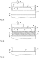
- Figures 2A - 2C illustrate one example of a method according to Figure 1 in greater detail.
- Each of Figures 2A - 2C shows a vertical cross sectional view of one example of a semiconductor wafer, Figures 2A and 2B further show an arrangement used to form a porous region in the semiconductor wafer.
- each of the first and second semiconductor layers 10, 20 is a doped semiconductor layer, wherein at least one of conditions (a) and (b) as outlined above is met with regard to a doping of the first semiconductor layer 10 and a doping of the second semiconductor layer 20.
- a current flows between the first and second electrode 41, 42 via the porosifying agent 50 and the first semiconductor layer 10, wherein the energy associated with this current causes the porosifying agent 50 to porosify the first semiconductor layer 10 in those regions that are in contact with the agent 50.
- the current flowing between the first and second electrodes 41, 42 is associated with a current density at the first surface 11 of the first semiconductor layer 10, wherein the current density in a certain region of the first surface 11 is given by the current flowing into that region divided an area of that region.
- the porosifying agent 50 includes hydrofluoric acid (HF).
- HF hydrofluoric acid
- an aqueous solution including HF is used as the porosifying agent 50.
- the porosifying agent 50 includes HF and ethanol such as an aqueous solution including HF and ethanol.
- the aqueous solution is such that a concentration of HF in the aqueous solution is between 20% and 25%.
- a polarity of the voltage V1 is such that an electrical potential of the first electrode 41 is more negative than an electrical potential of the second electrode 42.
- the second electrode 42 acts as an anode and the first electrode 41 acts as a cathode in the porosification process.
- the porosifying agent 50 forms a porous region 12 in the first semiconductor layer 10.
- the porosification starts at the first surface 11. That is, at first, the porous region 12 is formed at the first surface 11 where the porosifying agent 50, at first, is in contact with the first semiconductor layer 10.
- the porosifying agent 50 penetrates the porous region 12, so that the porous region 12 further extends into the first semiconductor layer 10.
- Figure 2B shows the porous region 12 formed by the porosification process.
- the porous region 12 in a vertical direction, extends from the first surface 11 of the semiconductor layer 10 through the first semiconductor layer 10 down to the second semiconductor layer 20.
- the porous region 12 may extend to the second semiconductor layer 20, but not into the second semiconductor layer 20. That is, the second semiconductor layer 20 may essentially remain unaffected by the porosification process.
- This can be achieved by implementing the first semiconductor layer 10 with a higher doping concentration than the second semiconductor layer 20 and/or with a doping type that is complementary to a doping type of the first semiconductor layer 10, as mentioned above.
- the first semiconductor layer 10 is a p-type (p-doped) layer and the second semiconductor layer 20 is an n-type (n-doped) layer.
- the reservoir accommodating the porosifying agent 50 is formed on top of the first surface 11 such that the porosifying agent 50, at the beginning of the porosification process is in contact with at least 80%, at least 90%, or at least 95% of the first surface 11 of the first semiconductor layer 10.
- the rim 13 is less than 20%, less than 10% or less than 5% of the first semiconductor layer 10.
- the second semiconductor layer 20 is essentially unaffected by the porosification process and the removal process. That is, most of the semiconductor layer 10 is removed down to the second semiconductor layer 20, while the second semiconductor layer 20 is essentially not removed.
- the thickness of the removed material is essentially given by the thickness of the first semiconductor layer 10, while the thickness of the second semiconductor layer 20 is essentially maintained.
- a first surface 21 of the second semiconductor layer 20 that is obtained by the removal process is essentially defined by an interface between the first semiconductor layer 10 and the second semiconductor layer 20 before the porosification process. In other words, the porosification and removal process essentially stops at this interface. This is independent of possible thickness variations of the first semiconductor layer, that is, independent of whether the surface 11 of the first layer 10 is planar or non-planar.
- the etching process can be a dry etching process such as a plasma etching process using at least one of Cl 2 , SF 6 , HBr, NF 3 , CF 4 or a wet etching process such as an etching process using a solution of HF and HNO 3 , a solution of TMAH (Tetramethylammonium hydroxide) and alcohol, or a solution of KOH and alcohol.
- TMAH Tetramethylammonium hydroxide
- a plurality of identical semiconductor devices have been formed in the second semiconductor layer 20 before partially removing the first semiconductor layer, and the wafer is finally divided up in order to form a plurality of single semiconductor devices.
- semiconductor device includes a discrete semiconductor device such as a transistor, a diode, a thyristor, or the like, but also an integrated circuit with a plurality of devices.
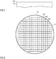
- Figure 5 schematically shows a top view of the wafer after partially removing the first semiconductor layer 10, that is, after the process illustrated in Figures 2A to 2C . More specifically, Figure 5 shows a top view of the rim 13 and of the first surface 21 of the second semiconductor layer 20, wherein this first surface 21 is uncovered by removing the porous region 12.
- reference number 100 schematically illustrates positions of a plurality of individual semiconductor devices. These semiconductor devices are located spaced apart from the edge surface 14 and the rim 13. The wafer is finally divided up along cutting lines located between the individual semiconductor devices in order to obtain a plurality of single semiconductor devices. According to one example, the rim 13 is removed before dividing up the wafer.
- the wafer is divided up without prior removal of the rim 13.
- the rim 13 is "automatically" removed, so that there is no need to remove the rim 13 beforehand.
- FIGs 7A-7B One example of how the porosification process can be improved in order to avoid a situation as illustrated in Figure 6 is illustrated in Figures 7A-7B .
- This example includes implementing the first semiconductor layer 10 such that a thickness of the first semiconductor layer 10 has a minimum in the center of the wafer and increases towards the edge surface 13.
- the first surface 11 is conical (as illustrated in Figure 7A ), dished (not shown) or the like.
- Figure 7A shows the wafer during the porosification process.
- a first surface 11 of this type can be obtained by a polishing or grinding process, for example.
- the porosification starts at the first surface 11 below the first electrode 41, and the porous region 12 extends from those sections of the first surface 11 that are located below the first electrode 41 in the vertical direction and in horizontal directions.
- the porous region 12 touches the second semiconductor layer 20 in the center of the wafer first, as illustrated in Figure 7A . From there, the porous region 12 further expands in horizontal directions until substantially the first semiconductor layer 10 is completely porosified below those sections of the first surface 11 that are in contact with the porosifying agent 50.
- the first electrode 41 has the form of a plate.
- the porosification process is improved by modifying the geometry of the first semiconductor layer 10.
- an improved porosification process can be achieved by suitably adjusting the current density at the first surface 11 during the porosification process.
- suitably adjusting the current density at the first surface 11 includes adjusting the current density such that the current density along the first surface 11, at least in sections, decreases between a center of the first semiconductor layer 10 and an edge region where the first semiconductor layer 10 is connected to the second electrode 42. "This is referred to a as lateral variation of the current density" in the following.
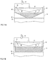
- FIG 8A shows the wafer during the porosification process.
- the porous region 12 starts to the formed below the first electrode 41 at the surface 11 of the first semiconductor layer 10 and, from there, expands in the vertical direction and in horizontal directions.
- porous region 12 touches the second semiconductor layer 20 in the center of the wafer first and, from there, further expands in horizontal directions.
- Figures 9A and 9B illustrate another example of a porosification process in which the current density decreases towards the edge region.
- the first electrode 41 has a plurality of electrode sections 41 1 -41 7 wherein a distance between these electrode sections 41 1 -41 7 and the first surface 11 increases as the distance of the respective electrode section to the center of the wafer increases.
- the more distant an electrode section 41 1 -41 7 is located from the center of the wafer in horizontal directions, the more distant the respective electrode section is located from the first surface 11 in the vertical direction and the lower is a current density at the first surface 11.
- the porosifying agent forms a resistor between the first electrode 41 and the first surface 11.
- the more distant a section of the electrode 41 is from the first surface 11, the higher is a resistance between the respective section of the first electrode 41 and the first surface 11, and the lower is the current density at the first surface 11 below the respective section of the first electrode 41).
- first electrode 41 of the type illustrated in Figure 10B connecting each of the rings 41 A -41 C to the voltage or current source 43 via a respective electronic switch 44 A -44 C , and activating (switching on) the switches 44 A -44 C successively such that at the beginning of the porosification process an innermost ring 41 A is connected to the voltage or current source 43, then the directly adjacent ring 41 B is connected to the voltage or current source 43, and so on.
- the rings 41 A -41 C may have the same distance from the surface 21.
- Figure 11A shows the wafer during the porosification process
- Figure 11B shows the wafer after the porosification process.
- the porous region 12 propagates faster into the first semiconductor layer 10 in the center of the wafer so that the porous region 12 touches the second semiconductor layer 20 in the center of the wafer first.
- Figure 12 illustrates the result of an imperfect porosification process according to another example.
- non-porosified regions (residuals) 16 of the first semiconductor layer 10 remain in a region close to the rim 13, that is, close to the edge surface 14 after the porosification process and the removal process.
- the first semiconductor layer 10 may include one or more of these residuals 16 that are spaced apart from each other or may include one residual 16 that extends along the rim 13 has essentially the form of a ring.
- FIG. 13 One example of a porosification process that is suitable to avoid residuals of the type illustrated in Figure 12 or that is suitable to at least to reduce the size of these residuals 16 is illustrated in Figure 13 .
- This porosification process is based on the porosification process illustrated in Figures 8A and 8B and is different from the porosification process illustrated in Figures 8A and 8B in that the current density in the edge region of the first surface 11 is reduced (as compared to the method according to Figures 8A and 8B ) by increasing a resistance between the first electrode 41 and the first surface 11 in the edge region, wherein increasing the resistance results in a further decrease of the current density in the edge region.
- reducing the active height of the porosifying agent 50 above the edge region of the first semiconductor layer 10 is achieved by providing an electrically insulating element 33 that adjoins the tubular element 31, extends inwardly from the tubular element 31, and is spaced apart from the first surface 11 of the first semiconductor layer 10.
- This element 33 may have the form of a ring in a section plane perpendicular to the section plane shown in Figure 13 .
- the first dimension d33 of the insulating element is between 1 centimeter (cm) and 3 centimeter. According to one example, a maximum distance between the insulating element 33 and the first surface 11 is 1.5 cm, in particular 1cm.
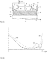
- Curve 203 illustrates the current density in a porosification process in which a ring 33 of the type shown in Figures 14 or 15 has been used. As can be seen from Figure 16 in this example, the current density in the edge region is lower than in the first scenario (see curve 201, no ring), so that the risk that residuals are formed is significantly reduced.
- the second semiconductor layer 20 is used to integrate semiconductor devices therein.
- the doping concentration of the second layer 20 is selected such that a selective porosification can be obtained and that semiconductor devices with desired electric characteristics can be achieved.
- the transistor device shown in Figures 18 and 19 is a vertical transistor device. It should be noted that a transistor device is only one example of a variety of vertical semiconductor devices that can be formed based on the second semiconductor layer 20. Further examples include, but are not restricted to, a vertical diode, a vertical thyristor, or the like.
- a doping concentration of the second semiconductor layer 20 is less than 1E-2 times the doping concentration of the first semiconductor layer in order to achieve a selective porosification process.
- a second semiconductor layer 20 with a doping concentration suitable to achieve a selective porosification process is not suitable for integrating active device regions such as drift regions of vertical transistor cells therein.
- the wafer may further include a third semiconductor layer 30 (illustrated in dashed lines in the drawings) on top of the second semiconductor layer 20, wherein the second semiconductor layer 20 is a thin layer with a thickness of less than 10 micrometers, for example.
Landscapes
- Chemical & Material Sciences (AREA)
- Chemical Kinetics & Catalysis (AREA)
- Engineering & Computer Science (AREA)
- Electrochemistry (AREA)
- Materials Engineering (AREA)
- Metallurgy (AREA)
- Organic Chemistry (AREA)
- Element Separation (AREA)
- General Chemical & Material Sciences (AREA)
- Weting (AREA)
- Bipolar Transistors (AREA)
- Metal-Oxide And Bipolar Metal-Oxide Semiconductor Integrated Circuits (AREA)
Abstract
Description
- This disclosure in general relates to a method for partially removing a semiconductor wafer.
- A semiconductor wafer that is used for forming vertical power semiconductor devices such as power transistors or power diodes may include a semiconductor substrate and a semiconductor layer, such as an epitaxial layer, formed on top of the semiconductor substrate. Based on one wafer a plurality of semiconductor devices can be formed at once, wherein the wafer is finally divided up in order to form a plurality of single semiconductor devices (semiconductor chips). The substrate acts as a carrier that serves to form the epitaxial layer thereon and that mechanically stabilizes the wafer during processing sequences that form the semiconductor devices. These processing sequences include, for example, forming doped regions in the epitaxial layer, forming passivation layers and/or metallization layers on top of the one or more epitaxial layers, or the like.
- In some cases, the substrate merely acts as a carrier and is finally removed. A further device region such as a drain region of a MOSFET (Metal Oxide Semiconductor Field-Effect Transistor), a collector region of an IGBT (Insulated Gate Bipolar Transistor), or an anode or cathode region of a diode may be formed in the epitaxial layer after removing the carrier. Ideally, only the substrate is removed so that the thickness of the semiconductor layer remains unchanged. This, however, is difficult to achieve using conventional removal techniques such as etching or polishing processes.
- There is therefore a need to precisely remove one section, such as a semiconductor substrate, of a semiconductor wafer while preserving other sections, such as a semiconductor layer that was previously formed on top of the substrate.
- One example relates to a method. The method includes, in a semiconductor wafer including a first semiconductor layer and a second semiconductor layer adjoining the first semiconductor layer, forming a porous region extending from a first surface into the first semiconductor layer, and removing the porous region by an etching process. With regard to a doping of the first semiconductor layer and a doping of the second semiconductor layer at least one of the following applies: a doping concentration of the second semiconductor layer is less than 10-2 times a doping concentration of the first semiconductor layer, or a doping type of the second semiconductor layer is complementary to a doping type of the first semiconductor layer.
- Examples are explained below with reference to the drawings. The drawings serve to illustrate certain principles, so that only aspects necessary for understanding these principles are illustrated. The drawings are not to scale. In the drawings the same reference characters denote like features.
-
Figure 1 shows a flowchart of one example of a method for partially removing a semiconductor wafer; -
Figures 2A - 2C show vertical cross sectional views of a semiconductor wafer during different process sequences of a method according toFigure 1 ; -
Figure 3 shows a top view of the arrangement shown inFigure 2A ; -
Figure 4 shows a vertical cross sectional view of the wafer after a further process sequence; -
Figure 5 shows a top view of one example of a wafer after the process step illustrated inFigure 2C ; -
Figure 6 shows a vertical cross sectional view of a wafer after an imperfect porosification process; -
Figures 7A - 7B ,8A - 8B ,9A - 9B illustrate different examples of a porosification process; -
Figures 10A and 10B show a horizontal cross sectional views of electrodes that may be used in the method according toFigures 9A to 9B ; -
Figures 11A and 11B illustrates a porosification process according to another example; -
Figure 12 illustrates the result of another example of an imperfect porosification process; -
Figures 13 - 15 illustrate different examples of porosification process processes suitable to avoid imperfections as illustrated inFigure 12B ; -
Figure 16 illustrates a current density during the porosification process dependent on a geometry of a reservoir used in the porosification process; -
Figures 17A to 17B show a porosification process according to another example; -
Figure 18 shows a vertical cross sectional view of a semiconductor device implemented in the semiconductor wafer before the porosification process; and -
Figure 19 shows a vertical cross sectional view of the semiconductor device shown inFigure 18 after partially removing the semiconductor wafer. - In the following detailed description, reference is made to the accompanying drawings. The drawings form a part of the description and for the purpose of illustration show examples of how the invention may be used and implemented. It is to be understood that the features of the various embodiments described herein may be combined with each other, unless specifically noted otherwise.
-
Figure 1 shows a flowchart of one example of a method for partially removing a semiconductor wafer. More specifically, the method relates to at least partially removing a first semiconductor layer of a semiconductor wafer that includes the first semiconductor layer and a second semiconductor layer adjoining the first semiconductor layer. Referring toFigure 1 , the method includes forming a porous region in the first semiconductor layer of the semiconductor wafer such that the porous region extends from a first surface into the first semiconductor layer. The process of forming the porous region in the first semiconductor layer is referred to as porosification process in the following. - With regard to a doping of the first semiconductor layer and a doping of the second semiconductor layer at least one of the following applies: (a) a doping concentration of the second semiconductor is less than 10-2 times a doping concentration of the first semiconductor layer; (b) a doping type of the second semiconductor layer is complementary to a doping type of the first semiconductor layer. The wafer can comply with both condition (a) and condition (b), that is, the first semiconductor layer and the second semiconductor layer can be layers of complementary doping types and the doping concentration of the second semiconductor layer is less than 10-2 (=1E-2) times the doping concentration of the first semiconductor layer, or the wafer can comply with only one of conditions (a) and (b). The "doping type" is either n or p so that when the wafer complies with condition (b) the first semiconductor layer is one of a p-doped (p-type) layer and an n-doped (n-type) layer and the second semiconductor layer is the other one of a p-doped (p-type) layer and an n-doped (n-type) layer. Further, "doping concentration" is the effective doping concentration.
- According to one example, the doping concentration of the first semiconductor layer is at least 1E3 times or at least 1E4 times the doping concentration of the second semiconductor layer. According to one example, the doping concentration of the first semiconductor layer higher than 1E18 cm-3, in particular higher than 1E19 cm-3 and the doping concentration of the second semiconductor layer is lower than 1E16 cm-3 or even lower than 1E14 cm-3.
- Referring to
Figure 1 , the method further includes removing the porous region by an etching process. A given volume of the porous region has a surface that is several hundred times the surface of a non-porous region of the same volume. Due to the greater surface the porous region can be etched significantly faster than a non-porous region. Thus, in the etching process the porous region is completely removed while adjoining non-porous regions are essentially not etched by the etching process. According to one example, the first semiconductor layer and the second semiconductor layer are adapted to one another such that the porous region is only formed in the first semiconductor layer, but not the second semiconductor layer so that in the overall process essentially only sections of the first semiconductor wafer are removed. - The latter is obtained by implementing the first semiconductor layer with a higher doping concentration than the second semiconductor layer, that is, by implementing the first semiconductor layer with a doping concentration that is at least 102 times the doping concentration of the second semiconductor layer. In general, the lower the doping concentration of the second semiconductor layer relative to the doping concentration of the first semiconductor layer the more selective is the porosification process. The more selective the porosification process is the smaller is the porosified portion of the second semiconductor layer relative to the porosified portion of the first semiconductor layer.
- According to one example, the first semiconductor layer is a semiconductor substrate, and the second semiconductor layer is an epitaxial layer formed on the substrate . According to one example, the second semiconductor layer has been formed by implanting and/or diffusing dopant atoms into a semiconductor substrate, wherein a remainder of the substrate forms the first semiconductor layer. In a doped substrate of a first doping type, a second semiconductor layer of the first doping and a lower doping concentration than a remainder of the substrate or a second semiconductor layer of a second doping type complementary to the first doping type can be formed by implanting and/or diffusing dopant atoms of the second doping type.
-
Figures 2A - 2C illustrate one example of a method according toFigure 1 in greater detail. Each ofFigures 2A - 2C shows a vertical cross sectional view of one example of a semiconductor wafer,Figures 2A and 2B further show an arrangement used to form a porous region in the semiconductor wafer. -
Figure 2A shows the wafer before the porosification process. Referring toFigure 2A , the wafer includes afirst semiconductor layer 10 and asecond semiconductor layer 20 adjoining thefirst semiconductor layer 10. According to one example each of the first andsecond semiconductor layers second semiconductor layers first semiconductor layer 10 and a doping of thesecond semiconductor layer 20. - Forming the porous region in the
first semiconductor layer 10 includes bringing aporosifying agent 50 in contact with afirst surface 11 of thefirst semiconductor layer 10, and applying a voltage V1 between thefirst semiconductor layer 10 and theporosifying agent 50. In the example illustrated inFigure 2A , applying the voltage V1 between thefirst semiconductor layer 10 and theporosifying agent 50 includes immerging afirst electrode 41 into theporosifying agent 50, contacting thefirst semiconductor layer 10 with asecond electrode 42, and applying the voltage V1 between thefirst electrode 41 and thesecond electrode 42. According to one example, the voltage V1 is a direct voltage (DC voltage) selected from between IV and 12V. According to another example, a current source (not shown) is connected between thefirst electrode 41 and thesecond electrode 42. - In either case, a current flows between the first and
second electrode porosifying agent 50 and thefirst semiconductor layer 10, wherein the energy associated with this current causes theporosifying agent 50 to porosify thefirst semiconductor layer 10 in those regions that are in contact with theagent 50. The current flowing between the first andsecond electrodes first surface 11 of thefirst semiconductor layer 10, wherein the current density in a certain region of thefirst surface 11 is given by the current flowing into that region divided an area of that region. Basically, the higher a current density in a certain region of thefirst surface 11 of thefirst semiconductor layer 10 the more efficient the porosification process is, that is, the faster the respective region of thefirst semiconductor layer 10 is porosified. - According to one example, the
porosifying agent 50 includes hydrofluoric acid (HF). According to one example, an aqueous solution including HF is used as theporosifying agent 50. According to another example, theporosifying agent 50 includes HF and ethanol such as an aqueous solution including HF and ethanol. According to one example, the aqueous solution is such that a concentration of HF in the aqueous solution is between 20% and 25%. According to one example, a polarity of the voltage V1 is such that an electrical potential of thefirst electrode 41 is more negative than an electrical potential of thesecond electrode 42. In this example, thesecond electrode 42 acts as an anode and thefirst electrode 41 acts as a cathode in the porosification process. - The
porosifying agent 50 is a liquid in the example illustrated inFigure 2A . In this example, bringing theporosifying agent 50 in contact with thefirst surface 11 of thefirst semiconductor layer 10 includes forming a reservoir by thefirst surface 11 of thefirst semiconductor layer 10 and atubular element 31, and at least partially filling the reservoir with theporosifying agent 50. Thetubular element 31 is in contact with thefirst surface 11 of thesemiconductor layer 10 and forms sidewalls of the reservoir, and thefirst surface 11 of thesemiconductor layer 10 forms a bottom of the reservoir. - After applying the voltage VI, the
porosifying agent 50 forms aporous region 12 in thefirst semiconductor layer 10. The porosification starts at thefirst surface 11. That is, at first, theporous region 12 is formed at thefirst surface 11 where theporosifying agent 50, at first, is in contact with thefirst semiconductor layer 10. Theporosifying agent 50 penetrates theporous region 12, so that theporous region 12 further extends into thefirst semiconductor layer 10.Figure 2B shows theporous region 12 formed by the porosification process. In this example, theporous region 12, in a vertical direction, extends from thefirst surface 11 of thesemiconductor layer 10 through thefirst semiconductor layer 10 down to thesecond semiconductor layer 20. In horizontal directions, a dimension of theporous region 12 is essentially given by an area of those sections of thefirst surface 11 that are in contact with theporosifying agent 50. In other words, in horizontal directions, the dimension of theporous region 12 is essentially given by the dimension of thetubular element 31 that forms the reservoir for theporosifying agent 50. The "vertical direction" is a direction perpendicular to thefirst surface 11 of thefirst semiconductor layer 10. "Horizontal directions" are directions parallel to thefirst surface 11. According to one example, theporous region 12 is formed such that it covers at least 80% of a volume of thefirst semiconductor layer 10. - Referring to
Figure 2B , theporous region 12 may extend to thesecond semiconductor layer 20, but not into thesecond semiconductor layer 20. That is, thesecond semiconductor layer 20 may essentially remain unaffected by the porosification process. This can be achieved by implementing thefirst semiconductor layer 10 with a higher doping concentration than thesecond semiconductor layer 20 and/or with a doping type that is complementary to a doping type of thefirst semiconductor layer 10, as mentioned above. According to one example, thefirst semiconductor layer 10 is a p-type (p-doped) layer and thesecond semiconductor layer 20 is an n-type (n-doped) layer. -
Figures 2A - 2C illustrate only a section of the second semiconductor layer, namely a section that adjoins thefirst semiconductor layer 10. In order to widely avoid that the porous region extends into thesecond semiconductor layer 20 at least the section of thesecond semiconductor layer 20 that adjoins thefirst semiconductor layer 10 has a much lower doping concentration than thefirst semiconductor layer 10. Thus, spaced apart from an interface formed between thefirst semiconductor layer 10 and thesecond semiconductor layer 20 thesecond semiconductor layer 20 may have a different doping concentration than at the interface. This is explained with reference to an example herein further below. -
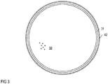
Figure 3 shows a top view of thetubular element 31 that forms sidewalls of the reservoir according to one example. In this example, thetubular element 31 forms a circular ring along an edge of the wafer. According to one example, thesecond electrode 42 is a ring-shaped electrode which, outside thetubular element 31, contacts thefirst semiconductor layer 10 along the edge of thefirst semiconductor layer 10. The first electrode is not shown inFigure 3 . The "edge" of thefirst semiconductor layer 10 is a section of thefirst surface 11 that adjoins anedge surface 14 of thefirst semiconductor layer 10. -
Figure 2C shows the wafer after removing the porosification means and after the etching process. The "porosification means" include the first andsecond electrodes porosifying agent 50 and means for forming the reservoir such as thetubular element 31 accommodating theporosifying agent 50. In the etching process, theporous region 12 is removed while non-porous regions essentially remain unaffected. In the example illustrated inFigures 2B and 2C , the non-porous region includes thesecond semiconductor layer 20 and asection 13 of thefirst semiconductor layer 10 that did not get in contact with theporosifying agent 50 in the porosification process. Thissection 13 adjoins theedge surface 14 of thefirst semiconductor layer 10. In horizontal directions, thissection 13 extends from theedge surface 14 to thetubular element 31 placed on top of thefirst surface 11 in the porosification process. Thissection 13 is referred to as edge region or rim. - According to one example, the reservoir accommodating the
porosifying agent 50 is formed on top of thefirst surface 11 such that theporosifying agent 50, at the beginning of the porosification process is in contact with at least 80%, at least 90%, or at least 95% of thefirst surface 11 of thefirst semiconductor layer 10. In this case and, when theporous region 12 is formed such that it extends down to thesecond semiconductor layer 20, therim 13 is less than 20%, less than 10% or less than 5% of thefirst semiconductor layer 10. Thus, by the method illustrated inFigures 2A to 2C , most of thefirst semiconductor layer 10 can be removed. - Further, due to the selectivity of the porosification process, the
second semiconductor layer 20 is essentially unaffected by the porosification process and the removal process. That is, most of thesemiconductor layer 10 is removed down to thesecond semiconductor layer 20, while thesecond semiconductor layer 20 is essentially not removed. Thus, in the vertical direction, the thickness of the removed material is essentially given by the thickness of thefirst semiconductor layer 10, while the thickness of thesecond semiconductor layer 20 is essentially maintained. Further, afirst surface 21 of thesecond semiconductor layer 20 that is obtained by the removal process is essentially defined by an interface between thefirst semiconductor layer 10 and thesecond semiconductor layer 20 before the porosification process. In other words, the porosification and removal process essentially stops at this interface. This is independent of possible thickness variations of the first semiconductor layer, that is, independent of whether thesurface 11 of thefirst layer 10 is planar or non-planar. - The etching process can be a dry etching process such as a plasma etching process using at least one of Cl2, SF6, HBr, NF3, CF4 or a wet etching process such as an etching process using a solution of HF and HNO3, a solution of TMAH (Tetramethylammonium hydroxide) and alcohol, or a solution of KOH and alcohol.
- According to one example, the wafer further includes a third semiconductor layer 30 (illustrated in dashed lines in
Figures 2A-2C ) adjoining thesecond semiconductor layer 20. In this example, thesecond semiconductor layer 20 may be a relatively thin layer with a thickness of less than 10 micrometers, less than 5 micrometers, or even less than 1 micrometer. According to one example, both thesecond semiconductor layer 20 and thethird semiconductor layer 30 are epitaxial layers. According to another example, the second semiconductor layer is formed by implanting and/or diffusing dopant atoms into the first semiconductor layer 10 (which may be a semiconductor substrate) and thethird semiconductor layer 30 is an epitaxial layer grown on thesecond semiconductor layer 20. According to one example, the method further includes removing therim 13. This may include a mechanical polishing process, a chemical-mechanical polishing (CMP) process or a laser cutting process. A vertical cross sectional view of the wafer after removing therim 13 is illustrated inFigure 4 . - According to one example, a plurality of identical semiconductor devices have been formed in the
second semiconductor layer 20 before partially removing the first semiconductor layer, and the wafer is finally divided up in order to form a plurality of single semiconductor devices. "Semiconductor device" as used herein includes a discrete semiconductor device such as a transistor, a diode, a thyristor, or the like, but also an integrated circuit with a plurality of devices.Figure 5 schematically shows a top view of the wafer after partially removing thefirst semiconductor layer 10, that is, after the process illustrated inFigures 2A to 2C . More specifically,Figure 5 shows a top view of therim 13 and of thefirst surface 21 of thesecond semiconductor layer 20, wherein thisfirst surface 21 is uncovered by removing theporous region 12. InFigure 5 ,reference number 100 schematically illustrates positions of a plurality of individual semiconductor devices. These semiconductor devices are located spaced apart from theedge surface 14 and therim 13. The wafer is finally divided up along cutting lines located between the individual semiconductor devices in order to obtain a plurality of single semiconductor devices. According to one example, therim 13 is removed before dividing up the wafer. - According to another example, the wafer is divided up without prior removal of the
rim 13. By dividing up the wafer therim 13 is "automatically" removed, so that there is no need to remove therim 13 beforehand. - Moreover, after partially removing the
first semiconductor layer 10 and before dividing up the wafer further process steps may be performed. These process steps include, for example, introducing dopant atoms via thefirst surface 21 into the second semiconductor layer, forming a metallization on thefirst surface 21, or the like. Therim 13 may help to stabilize the wafer during these process steps. - Referring to the above, it is desirable to porosify the
first semiconductor layer 10 below those sections of thefirst surface 11 that are in contact with theporosifying agent 50 and that extend down to thesecond semiconductor layer 20. It is undesirable that, except for therim 13, non-porosified regions of thefirst semiconductor layer 10 remain after the porosification process.Figure 6 shows a vertical cross sectional view of the wafer after an imperfect porosification process. At the end of this porosification process, a non-porosified section 15 (which is also referred to as residual 15 in the following) of thefirst semiconductor layer 10 remains. Within thefirst semiconductor layer 10 thisnon-porosified region 15 is surrounded by theporous region 12. In this example, theporous region 12 separates thenon-porous region 15 from those sections of thefirst semiconductor layer 10 which are connected to thesecond electrode 42 and the porous region prevents the residual from being further porosified. - In order to avoid a situation as illustrated in
Figure 6 , it is desirable to control the porosification process such that during the porosification process, theporous region 12 touches thesecond semiconductor layer 20 in a center of the wafer first, and then further expands in lateral directions towards theedge surface 14. Some examples of how this can be achieved are explained in the following. - One example of how the porosification process can be improved in order to avoid a situation as illustrated in
Figure 6 is illustrated inFigures 7A-7B . This example includes implementing thefirst semiconductor layer 10 such that a thickness of thefirst semiconductor layer 10 has a minimum in the center of the wafer and increases towards theedge surface 13. In this case, thefirst surface 11 is conical (as illustrated inFigure 7A ), dished (not shown) or the like.Figure 7A shows the wafer during the porosification process. Afirst surface 11 of this type can be obtained by a polishing or grinding process, for example. - As can be seen from
Figure 7A , the porosification starts at thefirst surface 11 below thefirst electrode 41, and theporous region 12 extends from those sections of thefirst surface 11 that are located below thefirst electrode 41 in the vertical direction and in horizontal directions. As thefirst semiconductor layer 10 has the lowest thickness in the center of the wafer, theporous region 12 touches thesecond semiconductor layer 20 in the center of the wafer first, as illustrated inFigure 7A . From there, theporous region 12 further expands in horizontal directions until substantially thefirst semiconductor layer 10 is completely porosified below those sections of thefirst surface 11 that are in contact with theporosifying agent 50. In the example illustrated inFigures 7A and 7B , thefirst electrode 41 has the form of a plate. According to one example, thefirst electrode 41 is arranged inside thetubular element 31 such that an edge of the plate-shapedfirst electrode 41 is equidistant to the tubular element. According to one example, an area of thefirst electrode 41 is at least 50%, or at least 75% of a cross sectional area of thetubular element 31. - In the examples illustrated in
Figures 7A and 7B , the porosification process is improved by modifying the geometry of thefirst semiconductor layer 10. Alternatively or additionally to modifying the geometry of thefirst semiconductor layer 10 an improved porosification process can be achieved by suitably adjusting the current density at thefirst surface 11 during the porosification process. According to one example, suitably adjusting the current density at thefirst surface 11 includes adjusting the current density such that the current density along thefirst surface 11, at least in sections, decreases between a center of thefirst semiconductor layer 10 and an edge region where thefirst semiconductor layer 10 is connected to thesecond electrode 42. "This is referred to a as lateral variation of the current density" in the following. -
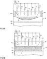
Figure 8A and 8B illustrate one example of a porosification process with a lateral variation of the current density. In this example, thefirst electrode 41 has the form of a needle. That is, a projection of thefirst electrode 41 onto thefirst surface 11 is much smaller than a cross sectional area of thetubular element 31. According to one example, the projection of the needle-shapedfirst electrode 41 onto thefirst surface 11 is less than 10% of the cross sectional area of thetubular element 31. Further, thefirst electrode 41, during the porosification process is located essentially above the center of the wafer. Due to the needle shapedfirst electrode 41 and the ring shaped second electrode 42 a variation of the current density is achieved such that the current density along thefirst surface 11 decreases from the center towards the edge region. Due to this, thefirst semiconductor layer 10 is porosified faster in the center than in the edge region. This is schematically illustrated inFigures 8A and 8B . -
Figure 8A shows the wafer during the porosification process. As can be seen fromFigure 8A , theporous region 12 starts to the formed below thefirst electrode 41 at thesurface 11 of thefirst semiconductor layer 10 and, from there, expands in the vertical direction and in horizontal directions. In this example,porous region 12 touches thesecond semiconductor layer 20 in the center of the wafer first and, from there, further expands in horizontal directions. -
Figures 9A and 9B illustrate another example of a porosification process in which the current density decreases towards the edge region. In this example, thefirst electrode 41 has a plurality of electrode sections 411-417 wherein a distance between these electrode sections 411-417 and thefirst surface 11 increases as the distance of the respective electrode section to the center of the wafer increases. In other words, the more distant an electrode section 411-417 is located from the center of the wafer in horizontal directions, the more distant the respective electrode section is located from thefirst surface 11 in the vertical direction and the lower is a current density at thefirst surface 11. (The porosifying agent forms a resistor between thefirst electrode 41 and thefirst surface 11. (The more distant a section of theelectrode 41 is from thefirst surface 11, the higher is a resistance between the respective section of thefirst electrode 41 and thefirst surface 11, and the lower is the current density at thefirst surface 11 below the respective section of the first electrode 41). -
Figure 9A shows the wafer during the porosification process. In this example, theporous region 12 expands faster in thefirst semiconductor layer 10 in those regions in which the electrode sections are closer to thefirst surface 11. Because a distance between thefirst surface 11 and anelectrode section 411 in the center of the wafer is smaller than the distances between thefirst surface 11 and the other electrode sections 412-417, the current density at thefirst surface 11 is higher in the center, so that theporous region 12 has the highest propagation rate in the center of the wafer so that theporous region 12 touches thesecond semiconductor layer 20 in the center of the wafer first.Figure 9B shows the wafer at the end of the porosification process. - A
first electrode 41 as shown inFigures 9A and 9B can be in the form of a ribbon-shaped electrode that is wound into the form of a spiral. A top view of such spiral-shapedfirst electrode 41 is illustrated inFigure 10A . - According to another example illustrated in
Figure 10B , theelectrode 41 includes several (two or more) concentric electrically conducting rings 41A-41C. According to one example, these rings are connected to the voltage orcurrent source 41 at the same time. - In the examples illustrated above, the current density at different locations of the
first surface 11 is essentially constant over the duration of the porosification process and decreases towards the edge region. According to another example, the current density is adjusted such that it varies over the duration of the porosification process such that the current density increases towards the edge region over the time of the porosification process. This may be achieved using afirst electrode 41 of the type illustrated inFigure 10B , connecting each of the rings 41A-41C to the voltage orcurrent source 43 via a respective electronic switch 44A-44C, and activating (switching on) the switches 44A-44C successively such that at the beginning of the porosification process aninnermost ring 41A is connected to the voltage orcurrent source 43, then the directlyadjacent ring 41B is connected to the voltage orcurrent source 43, and so on. In other words, the more distant a ring 41A-41C is from a center of the ring configuration the later it is connected to the voltage orcurrent source 43 in the porosification process, so that the current density increases over the time towards the edge region. In this example, the rings 41A-41C may have the same distance from thesurface 21. -
Figures 11A and 11B illustrate another example of a porosification process in which the current density at each position of thefirst surface 11 is essentially constant over the time and varies in the lateral direction such that it decreases towards the edge surface. In this example, thefirst surface 11 of thefirst semiconductor layer 10 is essentially planar and thefirst electrode 41 has a form such that a distance between thefirst electrode 41 and thefirst surface 11 increases towards thetubular element 31 and, therefore, towards the edge region. In the example illustrated inFigures 11A and 11B , a surface of thefirst electrode 41 that faces thefirst surface 11 of the first semiconductor wafer is conical. This, however, is only an example. According to another example (not shown), this surface is convex or has the form of a truncated cone.Figure 11A shows the wafer during the porosification process, andFigure 11B shows the wafer after the porosification process. In this example, theporous region 12 propagates faster into thefirst semiconductor layer 10 in the center of the wafer so that theporous region 12 touches thesecond semiconductor layer 20 in the center of the wafer first. -
Figure 12 illustrates the result of an imperfect porosification process according to another example. In this example, non-porosified regions (residuals) 16 of thefirst semiconductor layer 10 remain in a region close to therim 13, that is, close to theedge surface 14 after the porosification process and the removal process. Thefirst semiconductor layer 10 may include one or more of theseresiduals 16 that are spaced apart from each other or may include one residual 16 that extends along therim 13 has essentially the form of a ring. - One example of a porosification process that is suitable to avoid residuals of the type illustrated in
Figure 12 or that is suitable to at least to reduce the size of theseresiduals 16 is illustrated inFigure 13 . This porosification process is based on the porosification process illustrated inFigures 8A and 8B and is different from the porosification process illustrated inFigures 8A and 8B in that the current density in the edge region of thefirst surface 11 is reduced (as compared to the method according toFigures 8A and 8B ) by increasing a resistance between thefirst electrode 41 and thefirst surface 11 in the edge region, wherein increasing the resistance results in a further decrease of the current density in the edge region. In this example, increasing the resistance includes locally reducing a cross section of a conducting channel formed by theporosifying agent 50 between thefirst electrode 41 and thefirst surface 11 of thefirst semiconductor layer 10. More specifically, locally reducing the cross section of the conducting channel includes reducing the cross section of the conducting channel above an edge region of thefirst semiconductor layer 10, wherein the edge region is spaced apart from the center and adjoins thetubular element 31. - In the example illustrated in
Figure 13 , the cross section of the conducting channel is reduced by reducing the height (thickness) of a portion of theporosifying agent 50 that is capable of conducting a current between thefirst electrode 41 and the edge region of thefirst semiconductor layer 10. The portion of the porosifying agent capable of conducting a current may be referred to as "active portion" and the height of the active portion may be referred to as "active height". - In the example illustrated in
Figure 13 , reducing the active height of theporosifying agent 50 above the edge region of thefirst semiconductor layer 10 is achieved by providing an electrically insulatingelement 33 that adjoins thetubular element 31, extends inwardly from thetubular element 31, and is spaced apart from thefirst surface 11 of thefirst semiconductor layer 10. Thiselement 33 may have the form of a ring in a section plane perpendicular to the section plane shown inFigure 13 . - In the example illustrated in
Figure 13 , only those sections of the porosifying agent that are located between the insulatingelement 33 and thefirst surface 11 are capable of conducting a current between thefirst electrode 41 and thefirst surface 11, while those sections located above the insulatingelement 33 and separated from thefirst surface 11 by the insulating element do not contribute to the conducting channel between thefirst electrode 41 and thefirst surface 11. - Referring to
Figure 13 , thering 33 extends inwardly from an inner surface of thetubular element 31. A first dimension d33 of thering 33 is a dimension of thering 33 in a direction from thetubular element 31 towards the center (that is, towards the first electrode 41) and in a plane that is parallel to thefirst surface 11 of thefirst semiconductor layer 10. According to one example, the first dimension d33 of thering 33 is between 5% and 70%, in particular between 10% and 50% of an inner radius r31 of thetubular element 31. The inner radius of thetubular element 31 is the distance between the center of the arrangement and the inner surface of thetubular element 31. According to another example, the first dimension d33 of the insulating element is between 1 centimeter (cm) and 3 centimeter. According to one example, a maximum distance between the insulatingelement 33 and thefirst surface 11 is 1.5 cm, in particular 1cm. - In the example illustrated in
Figure 13 , thefirst electrode 41 is a needle-shapedelectrode 41. This, however, is only an example. Any other type offirst electrode 41 explained herein before may be used in the method illustrated inFigure 13 as well. - In the example illustrated in
Figure 13 , afirst surface 34 of thering 33, which is a surface that faces thesurface 11 of thefirst semiconductor layer 10, is essentially parallel to thesurface 11 of thesemiconductor layer 10. In this case, a liquid level of theporosifying agent 50 below thering 33 is essentially the same at each position of thering 33. - According to another example illustrated in
Figure 14 , thesurface 34 of thering 33 is inclined relative to a plane that is parallel to thesurface 11 of thefirst semiconductor layer 10. According to one example, an angle γ between thefirst surface 34 of thering 33 and the plane parallel to thefirst surface 11 of thefirst semiconductor layer 10 is between 0° and 45°, in particular between 1° and 15°. - In the example illustrated in
Figure 14 , the insulatingelement 33 is essentially planar, so that the active height of the porosifying agent linearly decreases as the distance to the inner surface of thetubular element 31 decreases. This, however, is only an example. According to another example (not illustrated) the insulating element may have any other kind of non-linear shape, such as a parabolic shape. - In the examples illustrated in
Figures 13 and 14 , the reduced active height of theporosifying agent 50 above the edge region of thefirst semiconductor layer 10 is achieved by using aring 33 that is attached to thetubular element 31 and is completely submerged in theporosifying agent 50. This, however, is only an example. - According to another example illustrated in
Figure 15 , thering 13 includes a collar that extends from thering 33 in a direction facing away from thefirst surface 11 of thefirst semiconductor layer 10. In this case, theporosifying agent 50 only fills the space below thering 33, but does not adjoin a surface of thering 33 opposite thefirst surface 34. With regard to the porosification process, however, there is no difference whether theporosifying agent 50 only fills the space between thering 33 and thefirst surface 11 or whether thering 33 is covered by theporosifying agent 50 also on the surface opposite thefirst surface 34. - The porosification process is associated with a current flow between the
first semiconductor layer 10 and thefirst electrode 41. Basically, the higher a current density at thefirst surface 11 of thefirst semiconductor layer 10 the more efficient the porosification process is, that is, the faster a respective region of thefirst semiconductor layer 10 is porosified.Figure 16 illustrate simulations of the current density at thefirst surface 11 of thefirst semiconductor layer 10 dependent on a distance to the center (represented by 0 inFigure 16 ) for different geometries of the reservoir formed by thetubular element 31 and thefirst semiconductor layer 10.Curve 201 represents a porosification process that only uses thetubular element 31 to define the reservoir. As can be seen fromFigure 16 , in this porosification process, the current density significantly increases towards the edge (represented by r31 inFigure 16 ) of thefirst semiconductor layer 10. In this case, there is a relatively high risk thatresiduals 16 of the type illustrated inFigure 12 may occur. -
Curve 202 illustrates the current density in a porosification process in which, in addition to thetubular element 31, the reservoir is defined by a ring of the type illustrated inFigure 13 . As can be seen fromFigure 16 in this example, the current density in the edge region, at least in sections, is lower than in the first scenario (seecurve 201, no ring), so that the risk that residuals are formed is significantly reduced. -
Curve 203 illustrates the current density in a porosification process in which aring 33 of the type shown inFigures 14 or15 has been used. As can be seen fromFigure 16 in this example, the current density in the edge region is lower than in the first scenario (seecurve 201, no ring), so that the risk that residuals are formed is significantly reduced. -
Figures 17A and 17B illustrate another example of a porosification process. In this example, the wafer is supported by aholder 60 and theholder 60 is placed in acontainer 32 that can be filled with theporosifying agent 50. Thefirst electrode 41 can be a plate shaped electrode that is essentially parallel to thefirst surface 11 of thefirst semiconductor layer 10. Theholder 60 is placed in thecontainer 32 such that thefirst surface 11 is essentially perpendicular to asurface 51 of theporosifying agent 50. During the porosification process, the position of the wafer is varied relative to thesurface 51 of theporosifying agent 50 such that theporosifying agent 50 gets in contact with thefirst surface 11 of thefirst semiconductor layer 10 close to one section of theedge surface 14 first. This is illustrated inFigure 17A . - The area of the
first surface 11 that gets in contact with theporosifying agent 50 increases during the porosification process over the time until the complete area not covered by theholder 60 is in contact with theporosifying agent 50. The position of the wafer relative to thesurface 51 of theporosifying agent 50 can be varied by maintaining the position of the wafer inside thecontainer 32 and gradually filling thecontainer 32 with theporosifying agent 50. This is illustrated inFigures 17A and 17B . Alternatively, thecontainer 32 is filled with the porosifying agent such that a filling level is constant and the wafer is slowly, with a controlled speed, immerged into theporosifying agent 50. - In the method illustrated in
Figures 17A and 17B , the current density at thefirst surface 11 varies over the time, wherein the variation of the current density is achieved by moving the wafer relative to theporosifying agent 50. The current density is essentially zero in those sections of thefirst surface 11 located outside theporosifying agent 50, and is different from zero, so that a porosifying process takes place, in those sections of the first surface arranged inside theporosifying agent 50. In the example illustrated inFigures 17A and 17B , in which thefirst electrode 41 has the shape of a plate that is essentially parallel to thefirst surface 11, the current density is essentially the same at each position of that section of thefirst surface 11 that is inside theporosifying agent 50. - According to one example, the
second semiconductor layer 20 is used to integrate semiconductor devices therein. In this case, the doping concentration of thesecond layer 20 is selected such that a selective porosification can be obtained and that semiconductor devices with desired electric characteristics can be achieved. - Referring to the above, one or more semiconductor devices can be integrated in the wafer, in particular in the
second semiconductor layer 20 of the wafer.Figures 18 and 19 show one example of a vertical semiconductor device integrated in thesecond semiconductor layer 20.Figure 18 shows the semiconductor device before partially removing thefirst semiconductor layer 10 andFigure 19 shows the semiconductor device after partially removing thefirst semiconductor layer 10 and further process steps. Each ofFigures 18 and 19 shows only one section of one transistor device, wherein, as outlined above, a plurality of transistor devices can be integrated in thesecond semiconductor layer 20. As used herein, "integrating a semiconductor in the second semiconductor layer" includes forming device structures of the semiconductor devices in thesecond semiconductor layer 20, but also on top of asecond surface 22. "Thesecond surface 22" is a surface facing away from thefirst semiconductor layer 10. - Just for the purpose of illustration, the transistor device shown in
Figures 18 and 19 is a vertical transistor device. It should be noted that a transistor device is only one example of a variety of vertical semiconductor devices that can be formed based on thesecond semiconductor layer 20. Further examples include, but are not restricted to, a vertical diode, a vertical thyristor, or the like. - Referring to
Figures 18 and 19 , the forming the transistor device includes forming a plurality oftransistor cells 70, wherein each of thesetransistor cells 70 includes abody region 71 in thesecond semiconductor layer 20, a source region 72 in thebody region 70, and a gate electrode 73 dielectrically insulated from thebody region 71 by a gate dielectric 74. Further, asource electrode 75 is formed on top of thesecond surface 22 such that it is connected to the source andbody regions 72, 71 of thetransistor cells 70. This source electrode 75 forms a source node or is connected to a source node S of the transistor device. Further, the gate electrodes 73 of theindividual transistor device 70 are connected to a common gate node G, wherein connections between the gate electrodes 73 and the gate node G are only schematically illustrated inFigures 18 and 19 . Just for the purpose of illustration, the gate electrodes 73 are planar gate electrodes in the example shown inFigure 19 . That is, the gate electrodes 73 are formed on top of thesecond surface 22 and insulated from thesource electrode 75. This, however, is only an example. According to another example (not illustrated) the gate electrodes 73 and the gate dielectrics 74 are arranged in trenches in thesecond layer 20. - The body and
source regions 71, 72 can be formed by introducing dopant atoms via thesecond surface 22 into thesecond semiconductor layer 20, wherein introducing the dopant atoms may include at least one of an implantation process and a diffusion process. Thesecond semiconductor layer 20 can be formed by epitaxially growing one or more epitaxial layers on the first semiconductor layer. The second semiconductor layer may have a basic doping. This basic doping may be formed by in-situ doping the one or more epitaxial layers during the epitaxial growth process. -
Drift regions 79 of the transistor cells may be formed by sections of the second semiconductor layer that have the basic doping. Optionally, eachtransistor cell 70 further includes acompensation region 76 that adjoins the body region 72. For example, thesecompensation regions 76 are formed by implanting and/or diffusing dopant atoms into the one or more epitaxial layers forming thesecond semiconductor layer 20. Referring toFigure 18 , thedrift regions 79 may be formed such that they extend down to thefirst semiconductor layer 10 and the compensation regions may be formed such that they are spaced apart from thefirst semiconductor layer 10. - Optionally, the transistor device further includes a field stop region 77 (illustrated in dashed lines in
Figures 18 and 19 ) of the same doping type as thedrift regions 75, but more highly doped. According to one example, thefield stop region 77 is spaced apart from thefirst semiconductor layer 10. Thefield stop region 77 can be formed in the process of forming thesecond semiconductor layer 20 on top of thefirst semiconductor layer 10. - The transistor device can be implemented as an n-type transistor device or as a p-type transistor device. In an n-type transistor device, the source regions 72 and the
drift regions 79 are n-doped and thebody regions 71 and theoptional compensation regions 76 are p-doped. In a p-type transistor device, the doping types of the individual device regions are complementary to the doping types of the corresponding device regions in an n-type transistor device. -
Figure 19 shows the transistor device after removing thefirst semiconductor layer 10 and further process steps. These process steps include introducing dopant atoms into thefirst surface 21 of thesecond semiconductor layer 20 in order to form adrain region 78 and forming adrain metallization 80 on top of thedrain region 78. This process steps may take place before removing therim 13 and dividing up the wafer as illustrated inFigure 5 . - The transistor device can be implemented as a MOSFET or as an IGBT. In a MOSFET, the
drain region 78 has the same doping type as the source and driftregions 72, 79, and in an IGBT the drain region (which may also be referred to as collector region) has a doping type that is complementary to the doping type of the source and driftregions 72, 79. - One relevant feature of a transistor device of the type illustrated in
Figures 18 and 19 is the on-resistance, which is an electrical resistance of the transistor device between thesource metallization 75 and thedrain metallization 80 in an on-state (switched-on state). The on-resistance is mainly dependent on a resistance of thedrift region 79 between thedrain region 78 and thebody region 71, wherein this resistance is dependent on a doping concentration of thedrift regions 79 and a length of thedrift regions 79, which is the distance between thedrain region 78 and channel regions. "Channel regions" are sections of the body regions 72 that adjoin the gate dielectrics 74. In the process of forming thesecond semiconductor layer 20 the doping concentration of thedrift region 79 can be adjusted with a high accuracy. Also a thickness of thesecond semiconductor layer 20, which is the dimension of thesecond semiconductor layer 20 between thefirst semiconductor layer 10 and thesecond surface 22, can be produced with a high accuracy. Referring to the above, the removal method explained above leaves thesecond semiconductor layer 20 essentially untouched. Thus, the thickness of thesecond semiconductor layer 20 is essentially the same before and after removing thefirst semiconductor layer 10. Thus, essentially no thickness variation of thesecond semiconductor layer 20 and, therefore, essentially no variation of the on-resistances of the transistor devices results from the removal process. Essentially no thickness variation includes, for example, that in an 8 inch wafer thickness variations of thesecond semiconductor layer 20 are less than 1.5 micrometers, or even less than 0.5 micrometer. - Referring to the above, a doping concentration of the
second semiconductor layer 20 is less than 1E-2 times the doping concentration of the first semiconductor layer in order to achieve a selective porosification process. In some cases, however, asecond semiconductor layer 20 with a doping concentration suitable to achieve a selective porosification process is not suitable for integrating active device regions such as drift regions of vertical transistor cells therein. Thus, referring to the above, the wafer may further include a third semiconductor layer 30 (illustrated in dashed lines in the drawings) on top of thesecond semiconductor layer 20, wherein thesecond semiconductor layer 20 is a thin layer with a thickness of less than 10 micrometers, for example. - In this example, active device regions such as
drift regions 79,body regions 71, and source regions 72 are integrated in the third semiconductor layer 30 (wherein thedrift region 79 and theoptional compensation regions 76 may be formed in the process of forming thethird semiconductor layer 30. The thinsecond semiconductor layer 20 is removed before forming thedrain region 78, for example. Alternatively, dopant atoms are implanted in thesecond semiconductor layer 20 for forming thedrain region 78, for example. - Although the present disclosure is not so limited, the following numbered examples demonstrate one or more aspects of the disclosure.
- Example 1. A method, including: in a semiconductor wafer including a first semiconductor layer and a second semiconductor layer adjoining the first semiconductor layer, forming a porous region extending from a first surface into the first semiconductor layer; and removing the porous region by an etching process, wherein with regard to a doping of the first semiconductor layer and a doping of the second semiconductor layer at least one of the following applies: a doping concentration of the second semiconductor layer is less than 10-2 times a doping concentration of the first semiconductor layer; a doping type of the second semiconductor layer is complementary to a doping type of the first semiconductor layer.
- Example 2. The method of example 1, wherein the porous region is formed such that it covers at least 80%, at least 90% or at least 95% of the volume of the first semiconductor layer.
- Example 3. The method of example 1 or 2, wherein the porous region is formed such that, in a vertical direction of the first layer, the porous region extends from the first surface to the second layer, and, in lateral directions of the first layer, the porous region extends from a center towards an edge surface of the first layer.
- Example 4. The method of any one of the preceding examples, wherein forming the porous region includes: bringing in contact a porosifying agent with the first layer; and applying a voltage between the first layer and a first electrode that is in contact with the porosifying agent.
- Example 5. The method of example 4, wherein bringing in contact the porosifying agent with the first layer includes: attaching a tubular element to the first surface; partially filling a reservoir formed by the tubular element and the first surface with the porosifying agent.
- Example 6. The method of any one of examples 4 to 5, wherein applying the voltage includes applying the voltage between the first electrode and an edge region of the first layer.
- Example 7. The method of any one of examples 4 to 6, wherein applying the voltage includes applying the voltage such that a current density of a current associated with the voltage, at least in sections, decreases at the first surface between a center and an edge region of the first semiconductor layer.
- Example 8. The method of example 7 or 8, wherein the first electrode is plate-shaped.
- Example 9. The method of example 7 or 8, wherein the first electrode is needle-shaped.
- Example 10. The method of example 7 or 8, wherein the first electrode is such that a distance between the first electrode and the first surface increases towards the edge region of the first layer.
- Example 11. The method of example 7 or 8, wherein the first electrode is conical.
- Example 12. The method of example 7 or 8, wherein the first electrode is spiral-shaped.
- Example 13. The method of example 7 or 8, wherein the first electrode includes several concentric rings.
- Example 14. The method of any one of examples 1 to 13, wherein the first surface is essentially planar.
- Example 15. The method of any one of examples 1 to 13, wherein a thickness of the first semiconductor layer increases towards an edge of the first layer.
- Example 16. The method of any of examples 7 to 15, wherein the reservoir further includes: at least one insulating element arranged above an edge region of the first semiconductor layer and configured to reduce an active height of the porosifying agent above the edge region as compared to the center of the first semiconductor layer.
- Example 17. The method of example 16, wherein the at least one insulating element includes a ring adjoining the tubular element and extending inwardly from the tubular element.
- Example 18. The method of example 17, wherein the ring has a first surface facing the first semiconductor layer, and wherein an angle between a plane parallel to the first surface of the first semiconductor layer and the first surface of the ring is between 0° and 45° or between 1° and 15°.
- Example 19. The method of example 17 or 18, wherein the ring has a first dimension in a direction perpendicular to the tubular element, wherein the tubular element has an inner radius, and wherein a ratio between the first dimension of the ring and the inner radius of the tubular element is between 0.05 and 0.7.
- Example 20. The method of any one of examples 16 to 19, wherein the active height of the porosifying agent above the edge region is less than 1 cm.
- Example 21. The method of example 4, wherein bringing in contact the porosifying agent with the first layer includes: gradually immerging the wafer into a container including the porosifying agent such that an area of the first surface that gets in contact with the porosifying agent increases during the porosification process over the time.
- Example 22. The method of any one of the preceding examples, further including: forming a plurality of transistor cells in the second semiconductor layer before forming the porous region and removing the porous region.
- Example 23. The method of example 22, further including: forming a drain region in the second semiconductor layer after removing the porous region.
- Example 24. The method of any one of the preceding examples, wherein the wafer further includes a third semiconductor layer on top of the second semiconductor layer, and wherein the second semiconductor layer has a thickness less than 10 micrometers, less than 5 micrometers, or less than 1 micrometer.
- Example 25. The method of example 24, further including: forming a plurality of transistor cells in the third semiconductor layer before forming the porous region.
- Example 26. The method of example 25, further including: removing the second semiconductor layer; and forming a drain region in the s third semiconductor layer after removing the porous region.
- Example 27. The method of example 25, further including: forming a drain region in the second semiconductor layer after removing the porous region.
- While the invention has been described with reference to illustrative examples, this description is not intended to be construed in a limiting sense. Various modifications and combinations of the illustrative examples, as well as other examples of the invention, will be apparent to persons skilled in the art upon reference to the description. It is therefore intended that the appended claims encompass any such modifications or examples.
Claims (14)
- A method, comprising:in a semiconductor wafer comprising a first semiconductor layer (10) and a second semiconductor layer (20) adjoining the first semiconductor layer (10), forming a porous region (12) extending from a first surface (11) into the first semiconductor layer (10); andremoving the porous region (12) by an etching process,wherein with regard to a doping of the first semiconductor layer (10) and a doping of the second semiconductor layer (20) at least one of the following applies:a doping concentration of the second semiconductor layer (20) is less than 10-2 times a doping concentration of the first semiconductor layer (10);a doping type of the second semiconductor layer is complementary to a doping type of the first semiconductor layer (10).
- The method of any one of the preceding claims, wherein forming the porous region (12) comprises:bringing in contact a porosifying agent (50) with the first layer (10); andapplying a voltage between the first layer (10) and a first electrode (41) that is in contact with the porosifying agent (50).
- The method of claim 2, wherein bringing in contact the porosifying agent (50) with the first layer (10) comprises:attaching a tubular element (31) to the first surface (11);partially filling a reservoir formed by the tubular element (31) and the first surface (11) with the porosifying agent (50).
- The method of any one of claims 2 to 3, wherein applying the voltage comprises applying the voltage between the first electrode (41) and an edge region of the first layer (10).
- The method of any one of claims 2 to 4,
wherein applying the voltage comprises applying the voltage such that a current density of a current associated with the voltage, at least in sections, decreases at the first surface (11) between a center and an edge region of the first semiconductor layer (10). - The method of claim 4 or 5, wherein the first electrode (41) is needle-shaped.
- The method of any of claims 3 to 6, wherein the reservoir further comprises:
at least one insulating element (33) arranged above an edge region of the first semiconductor layer (10) and configured to reduce an active height of the porosifying agent (50) above the edge region as compared to the center of the first semiconductor layer (10). - The method of claim 7,
wherein the at least one insulating element comprises a ring (33) adjoining the tubular element (31) and extending inwardly from the tubular element (31). - The method of claim 3, wherein bringing in contact the porosifying agent (50) with the first layer (10) comprises:
gradually immerging the wafer into a container (32) comprising the porosifying agent (50) such that an area of the first surface (11) that gets in contact with the porosifying agent (50) increases during the porosification process over the time. - The method of any one of the preceding claims, further comprising:
forming a plurality of transistor cells (70) in the second semiconductor layer (20) before forming the porous region (12) and removing the porous region (12). - The method of any one of the preceding claims,
wherein the wafer further comprises a third semiconductor layer (30) on top of the second semiconductor layer (20), and
wherein the second semiconductor layer (20) has a thickness less than 10 micrometers, less than 5 micrometers, or less than 1 micrometer. - The method of claim 11, further comprising:
forming a plurality of transistor cells (70) in the third semiconductor layer (30) before forming the porous region (12). - The method of claim 12, further comprising:removing the second semiconductor layer (20); andforming a drain region (79) in the third semiconductor layer (30) after removing the porous region (12).
- The method of claim 12, further comprising:
forming a drain region (79) in the second semiconductor layer (20) after removing the porous region (12).
Priority Applications (2)
| Application Number | Priority Date | Filing Date | Title |
|---|---|---|---|
| US16/677,801 US11404262B2 (en) | 2018-11-23 | 2019-11-08 | Method for partially removing a semiconductor wafer |
| US17/841,781 US11810779B2 (en) | 2018-11-23 | 2022-06-16 | Method of porosifying part of a semiconductor wafer |
Applications Claiming Priority (1)
| Application Number | Priority Date | Filing Date | Title |
|---|---|---|---|
| DE102018129594.4A DE102018129594B4 (en) | 2018-11-23 | 2018-11-23 | PARTIAL REMOVAL OF A SEMICONDUCTOR WAFER |
Publications (3)
| Publication Number | Publication Date |
|---|---|
| EP3667706A2 true EP3667706A2 (en) | 2020-06-17 |
| EP3667706A3 EP3667706A3 (en) | 2020-11-25 |
| EP3667706B1 EP3667706B1 (en) | 2024-01-17 |
Family
ID=68295948
Family Applications (1)
| Application Number | Title | Priority Date | Filing Date |
|---|---|---|---|
| EP19202851.2A Active EP3667706B1 (en) | 2018-11-23 | 2019-10-11 | Partially removing a semiconductor wafer |
Country Status (3)
| Country | Link |
|---|---|
| US (2) | US11404262B2 (en) |
| EP (1) | EP3667706B1 (en) |
| DE (1) | DE102018129594B4 (en) |
Families Citing this family (1)
| Publication number | Priority date | Publication date | Assignee | Title |
|---|---|---|---|---|
| DE102018129594B4 (en) * | 2018-11-23 | 2025-09-04 | Infineon Technologies Ag | PARTIAL REMOVAL OF A SEMICONDUCTOR WAFER |
Family Cites Families (10)
| Publication number | Priority date | Publication date | Assignee | Title |
|---|---|---|---|---|
| US6921467B2 (en) * | 1996-07-15 | 2005-07-26 | Semitool, Inc. | Processing tools, components of processing tools, and method of making and using same for electrochemical processing of microelectronic workpieces |
| US6664169B1 (en) * | 1999-06-08 | 2003-12-16 | Canon Kabushiki Kaisha | Process for producing semiconductor member, process for producing solar cell, and anodizing apparatus |
| DE10161202C1 (en) * | 2001-12-13 | 2003-05-08 | Bosch Gmbh Robert | Reducing the thickness of a silicon substrate which has been made porous comprises making porous the rear side of the substrate lying opposite a front side which has been made porous, then removing the porous material formed |
| DE10345447B4 (en) * | 2003-09-30 | 2007-04-26 | Infineon Technologies Ag | Method for producing a semiconductor component |
| US20060046499A1 (en) * | 2004-08-20 | 2006-03-02 | Dolechek Kert L | Apparatus for use in thinning a semiconductor workpiece |
| US8313632B2 (en) * | 2005-05-18 | 2012-11-20 | Panasonic Corporation | Process of making an optical lens |
| US9624597B2 (en) * | 2013-06-13 | 2017-04-18 | Yan Ye | Methods and apparatuses for delaminating process pieces |
| US9217206B2 (en) * | 2013-09-27 | 2015-12-22 | Sunpower Corporation | Enhanced porosification |
| US9922838B2 (en) * | 2014-02-10 | 2018-03-20 | Rensselaer Polytechnic Institute | Selective, electrochemical etching of a semiconductor |
| DE102018129594B4 (en) * | 2018-11-23 | 2025-09-04 | Infineon Technologies Ag | PARTIAL REMOVAL OF A SEMICONDUCTOR WAFER |
-
2018
- 2018-11-23 DE DE102018129594.4A patent/DE102018129594B4/en active Active
-
2019
- 2019-10-11 EP EP19202851.2A patent/EP3667706B1/en active Active
- 2019-11-08 US US16/677,801 patent/US11404262B2/en active Active
-
2022
- 2022-06-16 US US17/841,781 patent/US11810779B2/en active Active
Also Published As
| Publication number | Publication date |
|---|---|
| EP3667706B1 (en) | 2024-01-17 |
| US20220310380A1 (en) | 2022-09-29 |
| US20200168449A1 (en) | 2020-05-28 |
| US11810779B2 (en) | 2023-11-07 |
| DE102018129594B4 (en) | 2025-09-04 |
| DE102018129594A1 (en) | 2020-05-28 |
| US11404262B2 (en) | 2022-08-02 |
| EP3667706A3 (en) | 2020-11-25 |
Similar Documents
| Publication | Publication Date | Title |
|---|---|---|
| CN109698230B (en) | IGBT with dV/dt controllability | |
| CN109698197B (en) | Method for producing an IGBT with dV/dt controllability | |
| US9396997B2 (en) | Method for producing a semiconductor component with insulated semiconductor mesas | |
| US9219143B2 (en) | Semiconductor device and super junction semiconductor device having semiconductor mesas | |
| CN103996701B (en) | A kind of super junction semiconductor device and its manufacturing method | |
| CN104465734B (en) | Insulated gate bipolar transistor and manufacturing method thereof | |
| CN102244091B (en) | Semiconductor component with a trench edge termination | |
| US10410911B2 (en) | Buried insulator regions and methods of formation thereof | |
| KR101955055B1 (en) | Power semiconductor device and method of fabricating the same | |
| JP2010045245A (en) | Semiconductor device and method of manufacturing semiconductor device | |
| CN108389787A (en) | Semiconductor devices and its manufacturing method | |
| US20170062562A1 (en) | Method for Producing a Semiconductor Device Having a Beveled Edge Termination | |
| US11227945B2 (en) | Transistor having at least one transistor cell with a field electrode | |
| CN107039502A (en) | Form the method and semiconductor devices of semiconductor devices | |
| US11810779B2 (en) | Method of porosifying part of a semiconductor wafer | |
| CN104347475B (en) | Edge termination structure with trench isolation regions | |
| US7956419B2 (en) | Trench IGBT with depletion stop layer | |
| US20160203977A1 (en) | Semiconductor Arrangement Including Buried Anodic Oxide and Manufacturing Method | |
| EP3511988B1 (en) | Semiconductor electronic device with trench gate and manufacturing method thereof | |
| US9178013B2 (en) | Semiconductor device with edge termination and method for manufacturing a semiconductor device | |
| US10608099B2 (en) | Methods of manufacturing semiconductor devices with a deep barrier layer |
Legal Events
| Date | Code | Title | Description |
|---|---|---|---|
| PUAI | Public reference made under article 153(3) epc to a published international application that has entered the european phase |
Free format text: ORIGINAL CODE: 0009012 |
|
| STAA | Information on the status of an ep patent application or granted ep patent |
Free format text: STATUS: THE APPLICATION HAS BEEN PUBLISHED |
|
| AK | Designated contracting states |
Kind code of ref document: A2 Designated state(s): AL AT BE BG CH CY CZ DE DK EE ES FI FR GB GR HR HU IE IS IT LI LT LU LV MC MK MT NL NO PL PT RO RS SE SI SK SM TR |
|
| AX | Request for extension of the european patent |
Extension state: BA ME |
|
| PUAL | Search report despatched |
Free format text: ORIGINAL CODE: 0009013 |
|
| AK | Designated contracting states |
Kind code of ref document: A3 Designated state(s): AL AT BE BG CH CY CZ DE DK EE ES FI FR GB GR HR HU IE IS IT LI LT LU LV MC MK MT NL NO PL PT RO RS SE SI SK SM TR |
|
| AX | Request for extension of the european patent |
Extension state: BA ME |
|
| RIC1 | Information provided on ipc code assigned before grant |
Ipc: H01L 21/3063 20060101AFI20201021BHEP Ipc: H01L 29/66 20060101ALI20201021BHEP Ipc: C25F 3/12 20060101ALI20201021BHEP |
|
| STAA | Information on the status of an ep patent application or granted ep patent |
Free format text: STATUS: REQUEST FOR EXAMINATION WAS MADE |
|
| 17P | Request for examination filed |
Effective date: 20210525 |
|
| RBV | Designated contracting states (corrected) |
Designated state(s): AL AT BE BG CH CY CZ DE DK EE ES FI FR GB GR HR HU IE IS IT LI LT LU LV MC MK MT NL NO PL PT RO RS SE SI SK SM TR |
|
| GRAP | Despatch of communication of intention to grant a patent |
Free format text: ORIGINAL CODE: EPIDOSNIGR1 |
|
| STAA | Information on the status of an ep patent application or granted ep patent |
Free format text: STATUS: GRANT OF PATENT IS INTENDED |
|
| RIC1 | Information provided on ipc code assigned before grant |
Ipc: C25F 3/12 20060101ALI20230710BHEP Ipc: H01L 29/66 20060101ALI20230710BHEP Ipc: H01L 29/78 20060101ALI20230710BHEP Ipc: H01L 29/739 20060101ALI20230710BHEP Ipc: H01L 29/06 20060101ALI20230710BHEP Ipc: H01L 21/3063 20060101AFI20230710BHEP |
|
| INTG | Intention to grant announced |
Effective date: 20230809 |
|
| P01 | Opt-out of the competence of the unified patent court (upc) registered |
Effective date: 20231011 |
|
| GRAS | Grant fee paid |
Free format text: ORIGINAL CODE: EPIDOSNIGR3 |
|
| GRAA | (expected) grant |
Free format text: ORIGINAL CODE: 0009210 |
|
| STAA | Information on the status of an ep patent application or granted ep patent |
Free format text: STATUS: THE PATENT HAS BEEN GRANTED |
|
| AK | Designated contracting states |
Kind code of ref document: B1 Designated state(s): AL AT BE BG CH CY CZ DE DK EE ES FI FR GB GR HR HU IE IS IT LI LT LU LV MC MK MT NL NO PL PT RO RS SE SI SK SM TR |
|
| REG | Reference to a national code |
Ref country code: GB Ref legal event code: FG4D |
|
| REG | Reference to a national code |
Ref country code: CH Ref legal event code: EP |
|
| REG | Reference to a national code |
Ref country code: DE Ref legal event code: R096 Ref document number: 602019045156 Country of ref document: DE |
|
| REG | Reference to a national code |
Ref country code: IE Ref legal event code: FG4D |
|
| REG | Reference to a national code |
Ref country code: LT Ref legal event code: MG9D |
|
| REG | Reference to a national code |
Ref country code: NL Ref legal event code: MP Effective date: 20240117 |
|
| REG | Reference to a national code |
Ref country code: AT Ref legal event code: MK05 Ref document number: 1651114 Country of ref document: AT Kind code of ref document: T Effective date: 20240117 |
|
| PG25 | Lapsed in a contracting state [announced via postgrant information from national office to epo] |
Ref country code: NL Free format text: LAPSE BECAUSE OF FAILURE TO SUBMIT A TRANSLATION OF THE DESCRIPTION OR TO PAY THE FEE WITHIN THE PRESCRIBED TIME-LIMIT Effective date: 20240117 |
|
| PG25 | Lapsed in a contracting state [announced via postgrant information from national office to epo] |
Ref country code: NL Free format text: LAPSE BECAUSE OF FAILURE TO SUBMIT A TRANSLATION OF THE DESCRIPTION OR TO PAY THE FEE WITHIN THE PRESCRIBED TIME-LIMIT Effective date: 20240117 |
|
| PG25 | Lapsed in a contracting state [announced via postgrant information from national office to epo] |
Ref country code: IS Free format text: LAPSE BECAUSE OF FAILURE TO SUBMIT A TRANSLATION OF THE DESCRIPTION OR TO PAY THE FEE WITHIN THE PRESCRIBED TIME-LIMIT Effective date: 20240517 |
|
| PG25 | Lapsed in a contracting state [announced via postgrant information from national office to epo] |
Ref country code: LT Free format text: LAPSE BECAUSE OF FAILURE TO SUBMIT A TRANSLATION OF THE DESCRIPTION OR TO PAY THE FEE WITHIN THE PRESCRIBED TIME-LIMIT Effective date: 20240117 |
|
| PG25 | Lapsed in a contracting state [announced via postgrant information from national office to epo] |
Ref country code: GR Free format text: LAPSE BECAUSE OF FAILURE TO SUBMIT A TRANSLATION OF THE DESCRIPTION OR TO PAY THE FEE WITHIN THE PRESCRIBED TIME-LIMIT Effective date: 20240418 |
|
| PG25 | Lapsed in a contracting state [announced via postgrant information from national office to epo] |
Ref country code: RS Free format text: LAPSE BECAUSE OF FAILURE TO SUBMIT A TRANSLATION OF THE DESCRIPTION OR TO PAY THE FEE WITHIN THE PRESCRIBED TIME-LIMIT Effective date: 20240417 Ref country code: HR Free format text: LAPSE BECAUSE OF FAILURE TO SUBMIT A TRANSLATION OF THE DESCRIPTION OR TO PAY THE FEE WITHIN THE PRESCRIBED TIME-LIMIT Effective date: 20240117 |
|
| PG25 | Lapsed in a contracting state [announced via postgrant information from national office to epo] |
Ref country code: ES Free format text: LAPSE BECAUSE OF FAILURE TO SUBMIT A TRANSLATION OF THE DESCRIPTION OR TO PAY THE FEE WITHIN THE PRESCRIBED TIME-LIMIT Effective date: 20240117 |
|
| PG25 | Lapsed in a contracting state [announced via postgrant information from national office to epo] |
Ref country code: AT Free format text: LAPSE BECAUSE OF FAILURE TO SUBMIT A TRANSLATION OF THE DESCRIPTION OR TO PAY THE FEE WITHIN THE PRESCRIBED TIME-LIMIT Effective date: 20240117 |
|
| PG25 | Lapsed in a contracting state [announced via postgrant information from national office to epo] |
Ref country code: RS Free format text: LAPSE BECAUSE OF FAILURE TO SUBMIT A TRANSLATION OF THE DESCRIPTION OR TO PAY THE FEE WITHIN THE PRESCRIBED TIME-LIMIT Effective date: 20240417 Ref country code: NO Free format text: LAPSE BECAUSE OF FAILURE TO SUBMIT A TRANSLATION OF THE DESCRIPTION OR TO PAY THE FEE WITHIN THE PRESCRIBED TIME-LIMIT Effective date: 20240417 Ref country code: LT Free format text: LAPSE BECAUSE OF FAILURE TO SUBMIT A TRANSLATION OF THE DESCRIPTION OR TO PAY THE FEE WITHIN THE PRESCRIBED TIME-LIMIT Effective date: 20240117 Ref country code: IS Free format text: LAPSE BECAUSE OF FAILURE TO SUBMIT A TRANSLATION OF THE DESCRIPTION OR TO PAY THE FEE WITHIN THE PRESCRIBED TIME-LIMIT Effective date: 20240517 Ref country code: HR Free format text: LAPSE BECAUSE OF FAILURE TO SUBMIT A TRANSLATION OF THE DESCRIPTION OR TO PAY THE FEE WITHIN THE PRESCRIBED TIME-LIMIT Effective date: 20240117 Ref country code: GR Free format text: LAPSE BECAUSE OF FAILURE TO SUBMIT A TRANSLATION OF THE DESCRIPTION OR TO PAY THE FEE WITHIN THE PRESCRIBED TIME-LIMIT Effective date: 20240418 Ref country code: FI Free format text: LAPSE BECAUSE OF FAILURE TO SUBMIT A TRANSLATION OF THE DESCRIPTION OR TO PAY THE FEE WITHIN THE PRESCRIBED TIME-LIMIT Effective date: 20240117 Ref country code: ES Free format text: LAPSE BECAUSE OF FAILURE TO SUBMIT A TRANSLATION OF THE DESCRIPTION OR TO PAY THE FEE WITHIN THE PRESCRIBED TIME-LIMIT Effective date: 20240117 Ref country code: BG Free format text: LAPSE BECAUSE OF FAILURE TO SUBMIT A TRANSLATION OF THE DESCRIPTION OR TO PAY THE FEE WITHIN THE PRESCRIBED TIME-LIMIT Effective date: 20240117 Ref country code: AT Free format text: LAPSE BECAUSE OF FAILURE TO SUBMIT A TRANSLATION OF THE DESCRIPTION OR TO PAY THE FEE WITHIN THE PRESCRIBED TIME-LIMIT Effective date: 20240117 |
|
| PG25 | Lapsed in a contracting state [announced via postgrant information from national office to epo] |
Ref country code: PL Free format text: LAPSE BECAUSE OF FAILURE TO SUBMIT A TRANSLATION OF THE DESCRIPTION OR TO PAY THE FEE WITHIN THE PRESCRIBED TIME-LIMIT Effective date: 20240117 Ref country code: PT Free format text: LAPSE BECAUSE OF FAILURE TO SUBMIT A TRANSLATION OF THE DESCRIPTION OR TO PAY THE FEE WITHIN THE PRESCRIBED TIME-LIMIT Effective date: 20240517 |
|
| PG25 | Lapsed in a contracting state [announced via postgrant information from national office to epo] |
Ref country code: SE Free format text: LAPSE BECAUSE OF FAILURE TO SUBMIT A TRANSLATION OF THE DESCRIPTION OR TO PAY THE FEE WITHIN THE PRESCRIBED TIME-LIMIT Effective date: 20240117 Ref country code: PT Free format text: LAPSE BECAUSE OF FAILURE TO SUBMIT A TRANSLATION OF THE DESCRIPTION OR TO PAY THE FEE WITHIN THE PRESCRIBED TIME-LIMIT Effective date: 20240517 Ref country code: PL Free format text: LAPSE BECAUSE OF FAILURE TO SUBMIT A TRANSLATION OF THE DESCRIPTION OR TO PAY THE FEE WITHIN THE PRESCRIBED TIME-LIMIT Effective date: 20240117 Ref country code: LV Free format text: LAPSE BECAUSE OF FAILURE TO SUBMIT A TRANSLATION OF THE DESCRIPTION OR TO PAY THE FEE WITHIN THE PRESCRIBED TIME-LIMIT Effective date: 20240117 |
|
| PG25 | Lapsed in a contracting state [announced via postgrant information from national office to epo] |
Ref country code: DK Free format text: LAPSE BECAUSE OF FAILURE TO SUBMIT A TRANSLATION OF THE DESCRIPTION OR TO PAY THE FEE WITHIN THE PRESCRIBED TIME-LIMIT Effective date: 20240117 |
|
| PG25 | Lapsed in a contracting state [announced via postgrant information from national office to epo] |
Ref country code: SM Free format text: LAPSE BECAUSE OF FAILURE TO SUBMIT A TRANSLATION OF THE DESCRIPTION OR TO PAY THE FEE WITHIN THE PRESCRIBED TIME-LIMIT Effective date: 20240117 |
|
| REG | Reference to a national code |
Ref country code: DE Ref legal event code: R097 Ref document number: 602019045156 Country of ref document: DE |
|
| PG25 | Lapsed in a contracting state [announced via postgrant information from national office to epo] |
Ref country code: EE Free format text: LAPSE BECAUSE OF FAILURE TO SUBMIT A TRANSLATION OF THE DESCRIPTION OR TO PAY THE FEE WITHIN THE PRESCRIBED TIME-LIMIT Effective date: 20240117 Ref country code: CZ Free format text: LAPSE BECAUSE OF FAILURE TO SUBMIT A TRANSLATION OF THE DESCRIPTION OR TO PAY THE FEE WITHIN THE PRESCRIBED TIME-LIMIT Effective date: 20240117 |
|
| PG25 | Lapsed in a contracting state [announced via postgrant information from national office to epo] |
Ref country code: SK Free format text: LAPSE BECAUSE OF FAILURE TO SUBMIT A TRANSLATION OF THE DESCRIPTION OR TO PAY THE FEE WITHIN THE PRESCRIBED TIME-LIMIT Effective date: 20240117 |
|
| PG25 | Lapsed in a contracting state [announced via postgrant information from national office to epo] |
Ref country code: SM Free format text: LAPSE BECAUSE OF FAILURE TO SUBMIT A TRANSLATION OF THE DESCRIPTION OR TO PAY THE FEE WITHIN THE PRESCRIBED TIME-LIMIT Effective date: 20240117 Ref country code: SK Free format text: LAPSE BECAUSE OF FAILURE TO SUBMIT A TRANSLATION OF THE DESCRIPTION OR TO PAY THE FEE WITHIN THE PRESCRIBED TIME-LIMIT Effective date: 20240117 Ref country code: RO Free format text: LAPSE BECAUSE OF FAILURE TO SUBMIT A TRANSLATION OF THE DESCRIPTION OR TO PAY THE FEE WITHIN THE PRESCRIBED TIME-LIMIT Effective date: 20240117 Ref country code: EE Free format text: LAPSE BECAUSE OF FAILURE TO SUBMIT A TRANSLATION OF THE DESCRIPTION OR TO PAY THE FEE WITHIN THE PRESCRIBED TIME-LIMIT Effective date: 20240117 Ref country code: DK Free format text: LAPSE BECAUSE OF FAILURE TO SUBMIT A TRANSLATION OF THE DESCRIPTION OR TO PAY THE FEE WITHIN THE PRESCRIBED TIME-LIMIT Effective date: 20240117 Ref country code: CZ Free format text: LAPSE BECAUSE OF FAILURE TO SUBMIT A TRANSLATION OF THE DESCRIPTION OR TO PAY THE FEE WITHIN THE PRESCRIBED TIME-LIMIT Effective date: 20240117 |
|
| PLBE | No opposition filed within time limit |
Free format text: ORIGINAL CODE: 0009261 |
|
| STAA | Information on the status of an ep patent application or granted ep patent |
Free format text: STATUS: NO OPPOSITION FILED WITHIN TIME LIMIT |
|
| PG25 | Lapsed in a contracting state [announced via postgrant information from national office to epo] |
Ref country code: IT Free format text: LAPSE BECAUSE OF FAILURE TO SUBMIT A TRANSLATION OF THE DESCRIPTION OR TO PAY THE FEE WITHIN THE PRESCRIBED TIME-LIMIT Effective date: 20240117 |
|
| 26N | No opposition filed |
Effective date: 20241018 |
|
| PG25 | Lapsed in a contracting state [announced via postgrant information from national office to epo] |
Ref country code: IT Free format text: LAPSE BECAUSE OF FAILURE TO SUBMIT A TRANSLATION OF THE DESCRIPTION OR TO PAY THE FEE WITHIN THE PRESCRIBED TIME-LIMIT Effective date: 20240117 |
|
| PG25 | Lapsed in a contracting state [announced via postgrant information from national office to epo] |
Ref country code: SI Free format text: LAPSE BECAUSE OF FAILURE TO SUBMIT A TRANSLATION OF THE DESCRIPTION OR TO PAY THE FEE WITHIN THE PRESCRIBED TIME-LIMIT Effective date: 20240117 |
|
| REG | Reference to a national code |
Ref country code: CH Ref legal event code: PL |
|
| GBPC | Gb: european patent ceased through non-payment of renewal fee |
Effective date: 20241011 |
|
| PG25 | Lapsed in a contracting state [announced via postgrant information from national office to epo] |
Ref country code: MC Free format text: LAPSE BECAUSE OF FAILURE TO SUBMIT A TRANSLATION OF THE DESCRIPTION OR TO PAY THE FEE WITHIN THE PRESCRIBED TIME-LIMIT Effective date: 20240117 |
|
| PG25 | Lapsed in a contracting state [announced via postgrant information from national office to epo] |
Ref country code: GB Free format text: LAPSE BECAUSE OF NON-PAYMENT OF DUE FEES Effective date: 20241011 |
|
| PG25 | Lapsed in a contracting state [announced via postgrant information from national office to epo] |
Ref country code: LU Free format text: LAPSE BECAUSE OF NON-PAYMENT OF DUE FEES Effective date: 20241011 Ref country code: BE Free format text: LAPSE BECAUSE OF NON-PAYMENT OF DUE FEES Effective date: 20241031 |
|
| PG25 | Lapsed in a contracting state [announced via postgrant information from national office to epo] |
Ref country code: FR Free format text: LAPSE BECAUSE OF NON-PAYMENT OF DUE FEES Effective date: 20241031 |
|
| PG25 | Lapsed in a contracting state [announced via postgrant information from national office to epo] |
Ref country code: CH Free format text: LAPSE BECAUSE OF NON-PAYMENT OF DUE FEES Effective date: 20241031 |
|
| REG | Reference to a national code |
Ref country code: BE Ref legal event code: MM Effective date: 20241031 |
|
| PG25 | Lapsed in a contracting state [announced via postgrant information from national office to epo] |
Ref country code: IE Free format text: LAPSE BECAUSE OF NON-PAYMENT OF DUE FEES Effective date: 20241011 |
|
| REG | Reference to a national code |
Ref country code: DE Ref legal event code: R079 Ref document number: 602019045156 Country of ref document: DE Free format text: PREVIOUS MAIN CLASS: H01L0021306300 Ipc: H10P0050640000 |
|
| PGFP | Annual fee paid to national office [announced via postgrant information from national office to epo] |
Ref country code: DE Payment date: 20251217 Year of fee payment: 7 |
|
| PG25 | Lapsed in a contracting state [announced via postgrant information from national office to epo] |
Ref country code: CY Free format text: LAPSE BECAUSE OF FAILURE TO SUBMIT A TRANSLATION OF THE DESCRIPTION OR TO PAY THE FEE WITHIN THE PRESCRIBED TIME-LIMIT; INVALID AB INITIO Effective date: 20191011 |
|
| PG25 | Lapsed in a contracting state [announced via postgrant information from national office to epo] |
Ref country code: HU Free format text: LAPSE BECAUSE OF FAILURE TO SUBMIT A TRANSLATION OF THE DESCRIPTION OR TO PAY THE FEE WITHIN THE PRESCRIBED TIME-LIMIT; INVALID AB INITIO Effective date: 20191011 |