EP3667652A1 - Display panel detection method and apparatus, detection device, and storage medium - Google Patents
Display panel detection method and apparatus, detection device, and storage medium Download PDFInfo
- Publication number
- EP3667652A1 EP3667652A1 EP18843763.6A EP18843763A EP3667652A1 EP 3667652 A1 EP3667652 A1 EP 3667652A1 EP 18843763 A EP18843763 A EP 18843763A EP 3667652 A1 EP3667652 A1 EP 3667652A1
- Authority
- EP
- European Patent Office
- Prior art keywords
- level
- signal
- voltage
- power source
- data
- Prior art date
- Legal status (The legal status is an assumption and is not a legal conclusion. Google has not performed a legal analysis and makes no representation as to the accuracy of the status listed.)
- Withdrawn
Links
- 238000001514 detection method Methods 0.000 title claims abstract description 87
- 238000000034 method Methods 0.000 claims abstract description 63
- 230000008569 process Effects 0.000 claims abstract description 35
- 230000009191 jumping Effects 0.000 claims abstract description 23
- 230000002950 deficient Effects 0.000 claims description 44
- 238000005259 measurement Methods 0.000 claims description 7
- 238000004590 computer program Methods 0.000 claims description 5
- 238000010586 diagram Methods 0.000 description 14
- 239000003990 capacitor Substances 0.000 description 13
- 229920001621 AMOLED Polymers 0.000 description 9
- 238000004088 simulation Methods 0.000 description 4
- 230000007547 defect Effects 0.000 description 3
- 238000007599 discharging Methods 0.000 description 2
- 230000000694 effects Effects 0.000 description 2
- 238000005516 engineering process Methods 0.000 description 2
- 239000002184 metal Substances 0.000 description 2
- 230000005540 biological transmission Effects 0.000 description 1
- 238000013500 data storage Methods 0.000 description 1
- 230000003247 decreasing effect Effects 0.000 description 1
- 230000006870 function Effects 0.000 description 1
- 238000004519 manufacturing process Methods 0.000 description 1
- 238000012986 modification Methods 0.000 description 1
- 230000004048 modification Effects 0.000 description 1
- 230000003287 optical effect Effects 0.000 description 1
- 230000008054 signal transmission Effects 0.000 description 1
- 238000006467 substitution reaction Methods 0.000 description 1
Images




Classifications
-
- G—PHYSICS
- G09—EDUCATION; CRYPTOGRAPHY; DISPLAY; ADVERTISING; SEALS
- G09G—ARRANGEMENTS OR CIRCUITS FOR CONTROL OF INDICATING DEVICES USING STATIC MEANS TO PRESENT VARIABLE INFORMATION
- G09G3/00—Control arrangements or circuits, of interest only in connection with visual indicators other than cathode-ray tubes
- G09G3/006—Electronic inspection or testing of displays and display drivers, e.g. of LED or LCD displays
-
- G—PHYSICS
- G09—EDUCATION; CRYPTOGRAPHY; DISPLAY; ADVERTISING; SEALS
- G09G—ARRANGEMENTS OR CIRCUITS FOR CONTROL OF INDICATING DEVICES USING STATIC MEANS TO PRESENT VARIABLE INFORMATION
- G09G3/00—Control arrangements or circuits, of interest only in connection with visual indicators other than cathode-ray tubes
- G09G3/20—Control arrangements or circuits, of interest only in connection with visual indicators other than cathode-ray tubes for presentation of an assembly of a number of characters, e.g. a page, by composing the assembly by combination of individual elements arranged in a matrix no fixed position being assigned to or needed to be assigned to the individual characters or partial characters
-
- G—PHYSICS
- G09—EDUCATION; CRYPTOGRAPHY; DISPLAY; ADVERTISING; SEALS
- G09G—ARRANGEMENTS OR CIRCUITS FOR CONTROL OF INDICATING DEVICES USING STATIC MEANS TO PRESENT VARIABLE INFORMATION
- G09G3/00—Control arrangements or circuits, of interest only in connection with visual indicators other than cathode-ray tubes
- G09G3/20—Control arrangements or circuits, of interest only in connection with visual indicators other than cathode-ray tubes for presentation of an assembly of a number of characters, e.g. a page, by composing the assembly by combination of individual elements arranged in a matrix no fixed position being assigned to or needed to be assigned to the individual characters or partial characters
- G09G3/22—Control arrangements or circuits, of interest only in connection with visual indicators other than cathode-ray tubes for presentation of an assembly of a number of characters, e.g. a page, by composing the assembly by combination of individual elements arranged in a matrix no fixed position being assigned to or needed to be assigned to the individual characters or partial characters using controlled light sources
- G09G3/30—Control arrangements or circuits, of interest only in connection with visual indicators other than cathode-ray tubes for presentation of an assembly of a number of characters, e.g. a page, by composing the assembly by combination of individual elements arranged in a matrix no fixed position being assigned to or needed to be assigned to the individual characters or partial characters using controlled light sources using electroluminescent panels
- G09G3/32—Control arrangements or circuits, of interest only in connection with visual indicators other than cathode-ray tubes for presentation of an assembly of a number of characters, e.g. a page, by composing the assembly by combination of individual elements arranged in a matrix no fixed position being assigned to or needed to be assigned to the individual characters or partial characters using controlled light sources using electroluminescent panels semiconductive, e.g. using light-emitting diodes [LED]
-
- G—PHYSICS
- G09—EDUCATION; CRYPTOGRAPHY; DISPLAY; ADVERTISING; SEALS
- G09G—ARRANGEMENTS OR CIRCUITS FOR CONTROL OF INDICATING DEVICES USING STATIC MEANS TO PRESENT VARIABLE INFORMATION
- G09G3/00—Control arrangements or circuits, of interest only in connection with visual indicators other than cathode-ray tubes
- G09G3/20—Control arrangements or circuits, of interest only in connection with visual indicators other than cathode-ray tubes for presentation of an assembly of a number of characters, e.g. a page, by composing the assembly by combination of individual elements arranged in a matrix no fixed position being assigned to or needed to be assigned to the individual characters or partial characters
- G09G3/22—Control arrangements or circuits, of interest only in connection with visual indicators other than cathode-ray tubes for presentation of an assembly of a number of characters, e.g. a page, by composing the assembly by combination of individual elements arranged in a matrix no fixed position being assigned to or needed to be assigned to the individual characters or partial characters using controlled light sources
- G09G3/30—Control arrangements or circuits, of interest only in connection with visual indicators other than cathode-ray tubes for presentation of an assembly of a number of characters, e.g. a page, by composing the assembly by combination of individual elements arranged in a matrix no fixed position being assigned to or needed to be assigned to the individual characters or partial characters using controlled light sources using electroluminescent panels
- G09G3/32—Control arrangements or circuits, of interest only in connection with visual indicators other than cathode-ray tubes for presentation of an assembly of a number of characters, e.g. a page, by composing the assembly by combination of individual elements arranged in a matrix no fixed position being assigned to or needed to be assigned to the individual characters or partial characters using controlled light sources using electroluminescent panels semiconductive, e.g. using light-emitting diodes [LED]
- G09G3/3208—Control arrangements or circuits, of interest only in connection with visual indicators other than cathode-ray tubes for presentation of an assembly of a number of characters, e.g. a page, by composing the assembly by combination of individual elements arranged in a matrix no fixed position being assigned to or needed to be assigned to the individual characters or partial characters using controlled light sources using electroluminescent panels semiconductive, e.g. using light-emitting diodes [LED] organic, e.g. using organic light-emitting diodes [OLED]
- G09G3/3225—Control arrangements or circuits, of interest only in connection with visual indicators other than cathode-ray tubes for presentation of an assembly of a number of characters, e.g. a page, by composing the assembly by combination of individual elements arranged in a matrix no fixed position being assigned to or needed to be assigned to the individual characters or partial characters using controlled light sources using electroluminescent panels semiconductive, e.g. using light-emitting diodes [LED] organic, e.g. using organic light-emitting diodes [OLED] using an active matrix
-
- G—PHYSICS
- G09—EDUCATION; CRYPTOGRAPHY; DISPLAY; ADVERTISING; SEALS
- G09G—ARRANGEMENTS OR CIRCUITS FOR CONTROL OF INDICATING DEVICES USING STATIC MEANS TO PRESENT VARIABLE INFORMATION
- G09G3/00—Control arrangements or circuits, of interest only in connection with visual indicators other than cathode-ray tubes
- G09G3/20—Control arrangements or circuits, of interest only in connection with visual indicators other than cathode-ray tubes for presentation of an assembly of a number of characters, e.g. a page, by composing the assembly by combination of individual elements arranged in a matrix no fixed position being assigned to or needed to be assigned to the individual characters or partial characters
- G09G3/22—Control arrangements or circuits, of interest only in connection with visual indicators other than cathode-ray tubes for presentation of an assembly of a number of characters, e.g. a page, by composing the assembly by combination of individual elements arranged in a matrix no fixed position being assigned to or needed to be assigned to the individual characters or partial characters using controlled light sources
- G09G3/30—Control arrangements or circuits, of interest only in connection with visual indicators other than cathode-ray tubes for presentation of an assembly of a number of characters, e.g. a page, by composing the assembly by combination of individual elements arranged in a matrix no fixed position being assigned to or needed to be assigned to the individual characters or partial characters using controlled light sources using electroluminescent panels
- G09G3/32—Control arrangements or circuits, of interest only in connection with visual indicators other than cathode-ray tubes for presentation of an assembly of a number of characters, e.g. a page, by composing the assembly by combination of individual elements arranged in a matrix no fixed position being assigned to or needed to be assigned to the individual characters or partial characters using controlled light sources using electroluminescent panels semiconductive, e.g. using light-emitting diodes [LED]
- G09G3/3208—Control arrangements or circuits, of interest only in connection with visual indicators other than cathode-ray tubes for presentation of an assembly of a number of characters, e.g. a page, by composing the assembly by combination of individual elements arranged in a matrix no fixed position being assigned to or needed to be assigned to the individual characters or partial characters using controlled light sources using electroluminescent panels semiconductive, e.g. using light-emitting diodes [LED] organic, e.g. using organic light-emitting diodes [OLED]
- G09G3/3225—Control arrangements or circuits, of interest only in connection with visual indicators other than cathode-ray tubes for presentation of an assembly of a number of characters, e.g. a page, by composing the assembly by combination of individual elements arranged in a matrix no fixed position being assigned to or needed to be assigned to the individual characters or partial characters using controlled light sources using electroluminescent panels semiconductive, e.g. using light-emitting diodes [LED] organic, e.g. using organic light-emitting diodes [OLED] using an active matrix
- G09G3/3233—Control arrangements or circuits, of interest only in connection with visual indicators other than cathode-ray tubes for presentation of an assembly of a number of characters, e.g. a page, by composing the assembly by combination of individual elements arranged in a matrix no fixed position being assigned to or needed to be assigned to the individual characters or partial characters using controlled light sources using electroluminescent panels semiconductive, e.g. using light-emitting diodes [LED] organic, e.g. using organic light-emitting diodes [OLED] using an active matrix with pixel circuitry controlling the current through the light-emitting element
-
- G—PHYSICS
- G09—EDUCATION; CRYPTOGRAPHY; DISPLAY; ADVERTISING; SEALS
- G09G—ARRANGEMENTS OR CIRCUITS FOR CONTROL OF INDICATING DEVICES USING STATIC MEANS TO PRESENT VARIABLE INFORMATION
- G09G2330/00—Aspects of power supply; Aspects of display protection and defect management
- G09G2330/12—Test circuits or failure detection circuits included in a display system, as permanent part thereof
Definitions
- an active-matrix organic light emitting diode (AMOLED) display panel as a new display panel on the market may comprise a plurality of data lines and a plurality of gate lines. Each two adjacent data lines and each two adjacent gate lines form a pixel unit in an enclosing manner. Each pixel unit corresponds to a driving circuit which is used for driving a corresponding pixel unit to emit light.
- AMOLED active-matrix organic light emitting diode
- the second transistor T2 may be in a turn-on state or in a turn-off state under the control of the first data signal D1.
- the power source end VDD can charge the pixel storage capacitor Cst, so that both the voltages at the two ends of the storage capacitor Cst are the voltage when the power source signal V is at the first level, and it can be measured that the first voltage of the pixel electrode ITO is the voltage when the power source signal V is at the first level.
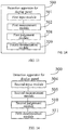
- Fig. 12 is a block diagram of a detection apparatus for a display panel provided in an embodiment of the present disclosure.
- the detection apparatus 50 for the display panel may comprise:
Landscapes
- Engineering & Computer Science (AREA)
- Physics & Mathematics (AREA)
- Computer Hardware Design (AREA)
- General Physics & Mathematics (AREA)
- Theoretical Computer Science (AREA)
- Control Of Indicators Other Than Cathode Ray Tubes (AREA)
Abstract
Description
- This application claims priority to Chinese Patent Application No.
201710672710.2 - The present disclosure relates to the field of display technology, and more particularly to a detection method and apparatus for display panel, a detection device and a storage medium.
- With the development of display technologies, various products having display functions appear in daily life, such as mobile phones, tablet computers, televisions, notebook computers, digital photo frames and navigators, each of which requires to be assembled with a display panel.
- Currently, an active-matrix organic light emitting diode (AMOLED) display panel as a new display panel on the market may comprise a plurality of data lines and a plurality of gate lines. Each two adjacent data lines and each two adjacent gate lines form a pixel unit in an enclosing manner. Each pixel unit corresponds to a driving circuit which is used for driving a corresponding pixel unit to emit light.
- The present disclosure provides a detection method and apparatus for display panel, a detection device and a storage medium. The technical solutions are as follows.
- In a first aspect, there is provided a detection method for a display panel, wherein the display panel comprises a plurality of data lines and a plurality of gate lines; the plurality of data lines and the plurality of gate lines intersect to form a plurality of pixel units in an enclosing manner; at least a part of the pixel units comprises a driving circuit and a pixel electrode; the driving circuit is connected to a data input end, a gate electrode scan input end and a power source end, respectively; and the method comprises: inputting a second data signal, a second gate line scan signal and a power source signal respectively to the data input end, the gate electrode scan input end and the power source end, wherein during the signal inputting process, the second data signal is at a first level, a level of the second gate line scan signal jumps from the first level to a second level, a level of the power source signal jumps from the first level to the second level, and the level of the second gate line scan signal jumps before the jumping of the level of the power source signal; measuring a second voltage of the pixel electrode in each pixel unit of the display panel; and determining a faulty gate line according to the second voltage.Optionally, the method further comprises: determining a faulty data line; and determining a position of a defective point in the display panel according to the faulty gate line and the faulty data line.
- Optionally, the defective point is a short-circuited defective point; and determining the faulty data line comprises: inputting a first data signal, a first gate line scan signal and a power source signal respectively to the data input end, the gate electrode scan input end and the power source end, wherein during the signal inputting process, the first gate line scan signal is at the first level, a level of the first data signal jumps from the first level to the second level, a level of the power source signal jumps from the first level to the second level, and the level of the first data signal jumps before the jumping of the level of the power source signal; measuring a first voltage of the pixel electrode in each pixel unit of the display panel; and determining the faulty data line according to the first voltage.
- Optionally, determining the faulty data line according to the first voltage comprises: judging whether the first voltage of the pixel electrode in each pixel unit is within a first preset voltage range; and determining that the data line corresponding to the pixel unit in which the first voltage is within the first preset voltage range is faulty, wherein a lower limit value in the first preset voltage range is greater than or equal to a voltage value when the power source signal is at the second level.
- Optionally, determining the faulty gate line according to the second voltage comprises: judging whether the second voltage of the pixel electrode in each pixel unit is within a second preset voltage range; and determining that the gate line corresponding to the pixel unit in which the second voltage is within the second preset voltage range is faulty, wherein a lower limit value in the second preset voltage range is greater than or equal to a voltage value when the power source signal is at the second level.
- Optionally, after measuring the first voltage of the pixel electrode in each pixel unit of the display panel, the method further comprises: judging whether the first voltage of the pixel electrode in each pixel unit is within a third preset voltage range; and determining that the data line corresponding to the pixel unit in which the first voltage is within the third preset voltage range is normal, wherein a lower limit value in the third preset voltage range is greater than an upper limit value in the first preset voltage range.
- Optionally, after measuring the second voltage of the pixel electrode in each pixel unit of the display panel, the method further comprises: judging whether the second voltage of the pixel electrode in each pixel unit is within a fourth preset voltage range; and determining that the gate line corresponding to the pixel unit in which the second voltage is within the fourth preset voltage range is normal, wherein a lower limit value in the fourth preset voltage range is greater than an upper limit value in the second preset voltage range.
- Optionally, when the first gate line scan signal is at the first level, the voltage value is 20 volts; when the first data signal is at the first level, the voltage value is 25 volts; when the first data signal is at the second level, the voltage value is -8 volts; when the power source signal is at the first level, the voltage value is 25 volts; and when the power source signal is at the second level, the voltage value is -15 volts; and when the second data signal is at the first level, the voltage value is 8 volts; when the second gate line scan signal is at the first level, the voltage value is 25 volts; and when the second gate line scan signal is at the second level, the voltage value is -25 volts.
- In a second aspect, there is provided a detection apparatus for a display panel, wherein the display panel comprises a plurality of data lines and a plurality of gate lines; the plurality of data lines and the plurality of gate lines intersect to form a plurality of pixel units in an enclosing manner; at least a part of the pixel units comprises a driving circuit and a pixel electrode; the driving circuit is connected to a data input end, a gate electrode scan input end and a power source end, respectively; and the apparatus comprises: a second input module configured to input a second data signal, a second gate line scan signal and a power source signal respectively to the data input end, the gate electrode scan input end and the power source end, wherein during the signal inputting process, the second data signal is at a first level, a level of the second gate line scan signal jumps from the first level to a second level, a level of the power source signal jumps from the first level to the second level, and the level of the second gate line scan signal jumps before the jumping of the level of the power source signal; a second measurement module configured to measure a second voltage of a pixel electrode in each pixel unit of the display panel; and a second determination module configured to determine a faulty gate line according to the second voltage.
- Optionally, the apparatus further comprises: a first determination module configured to determine a faulty data line; and a third determination module configured to determine a position of a defective point in the display panel according to the faulty gate line and the faulty data line.
- Optionally, the defective point is a short-circuited defective point, and the apparatus further comprises: a first input module configured to input a first data signal, a first gate line scan signal and a power source signal respectively to the data input end, the gate electrode scan input end and the power source end, wherein during the signal inputting process, the first gate line scan signal is at the first level, a level of the first data signal jumps from the first level to the second level, a level of the power source signal jumps from the first level to the second level, and the level of the first data signal jumps before the jumping of the level of the power source signal; a first measurement module configured to measure a first voltage of the pixel electrode in each pixel unit of the display panel; and a first determination module configured to determine a faulty data line according to the first voltage.
- Optionally, the first determination module is configured to: judge whether the first voltage of the pixel electrode in each pixel unit is within a first preset voltage range, and determine that the data line corresponding to the pixel unit in which the first voltage is within the first preset voltage range is faulty, wherein a lower limit value in the first preset voltage range is greater than or equal to a voltage value when the power source signal is at the second level.
- Optionally, the second determination module is configured to: judge whether the second voltage of the pixel electrode in each pixel unit is within a second preset voltage range; and determine that the gate line corresponding to the pixel unit in which the second voltage is within the second preset voltage range is faulty, wherein a lower limit value in the second preset voltage range is greater than or equal to a voltage value when the power source signal is at the second level.
- Optionally, the apparatus further comprises: a first judgment module configured to judge whether the first voltage of the pixel electrode in each pixel unit is within a third preset voltage range; and a fourth determination module configured to determine that the data line corresponding to the pixel unit in which the first voltage is in the third preset voltage range is normal, wherein a lower limit value in the third preset voltage range is greater than an upper limit value in the first preset voltage range.
- Optionally, the apparatus further comprises: a second judgment module configured to judge whether the second voltage of the pixel electrode in each pixel unit is within a fourth preset voltage range; and a fifth determination module configured to determine that the gate line corresponding to the pixel unit in which the second voltage is in the fourth preset voltage range is normal, wherein a lower limit value in the fourth preset voltage range is greater than an upper limit value in the second preset voltage range.
- Optionally, when the first gate line scan signal is at the first level, the voltage value is 20 volts; when the first data signal is at the first level, the voltage value is 25 volts; when the first data signal is at the second level, the voltage value is -8 volts; when the power source signal is at the first level, the voltage value is 25 volts; when the power source signal is at the second level, the voltage value is -15 volts; and when the second data signal is at the first level, the voltage value is 8 volts; when the second gate line scan signal is at the first level, the voltage value is 25 volts; and when the second gate line scan signal is at the second level, the voltage value is -25 volts.
- In a third aspect, there is provided a detection device for detecting a display panel, wherein the display panel comprises a plurality of data lines and a plurality of gate lines; the plurality of data lines and the plurality of gate lines intersect to form a plurality of pixel units in an enclosing manner; at least a part of the pixel units comprises a driving circuit and a pixel electrode; the driving circuit is connected to a data input end, a gate electrode scan input end and a power source end, respectively; and the detection device comprises: a processor, and a memory storing one or more programs executed by the processor, and the one or more programs includes instructions for performing the following operations: inputting a second data signal, a second gate line scan signal and a power source signal respectively to the data input end, the gate electrode scan input end and the power source end, wherein during the signal inputting process, the second data signal is at a first level, a level of the second gate line scan signal jumps from the first level to a second level, a level of the power source signal jumps from the first level to the second level, and the level of the second gate line scan signal jumps before the jumping of the level of the power source signal; measuring a second voltage of the pixel electrode in each pixel unit of the display panel; and determining a faulty gate line according to the second voltage.
- Optionally, the one or more programs include instructions for performing the following operations: determining a faulty data line; and determining a position of a defective point in the display panel according to the faulty gate line and the faulty data line.
- Optionally, the defective point is a short-circuited defective point, and the one or more programs include instructions for performing the following operations: inputting a first data signal, a first gate line scan signal and a power source signal respectively to the data input end, the gate electrode scan input end and the power source end, wherein during the signal inputting process, the first gate line scan signal is at the first level, a level of the first data signal jumps from the first level to the second level, a level of the power source signal jumps from the first level to the second level, and the level of the first data signal jumps before the jumping of the level of the power source signal; measuring a first voltage of the pixel electrode in each pixel unit of the display panel; and determining the faulty data line according to the first voltage.
- In a fourth aspect, there is provided a computer-readable storage medium storing a computer program, wherein the stored computer program is executed by a processor for implementing the detection method for the display panel of any of the above aspects.
- In order to describe the technical solutions in the embodiments of the present more clearly, the following briefly introduces the accompanying drawings required for describing the embodiments. Apparently, the accompanying drawings in the following description show merely some embodiments of the present disclosure, and a person of ordinary skill in the art may also derive other drawings from these accompanying drawings without creative efforts.
-
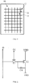
Fig. 1 is a schematic view of a structure of a display panel provided in an embodiment of the present disclosure; -
Fig. 2 is a schematic view of a structure of a driving circuit provided in an embodiment of the present disclosure; -
Fig. 3 is a schematic view of an effect of a display panel mounted on a detection device provided in the embodiment of the present disclosure; -
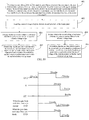
Fig. 4 is a flow chart of a detection method for a display panel provided in an embodiment of the present disclosure; -
Fig. 5 is a flow chart of a detection method for another display panel provided in an embodiment of the present disclosure; -
Fig. 6 is a timing sequence diagram of each signal end in a detection process provided in an embodiment of the present disclosure; -
Fig. 7 is a flow chart of a detection method for another display panel provided in an embodiment of the present disclosure; -
Fig. 8 is a diagram of an analogue simulation of a first voltage which measures a pixel electrode ITO provided in an embodiment of the present disclosure; -
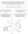
Fig. 9 is a timing sequence diagram of each signal end in another detection process provided in an embodiment of the present disclosure; -
Fig. 10 is a flow chart of a detection method for yet another display panel provided in an embodiment of the present disclosure; -
Fig. 11 is a diagram of an analogue simulation of a second voltage which measures a pixel electrode ITO provided in an embodiment of the present disclosure;Fig. 12 is a block diagram of a detection apparatus for a display panel provided in an embodiment of the present disclosure; -
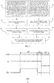
Fig. 13 is a block diagram of a detection apparatus for another display panel provided in an embodiment of the present disclosure; -
Fig. 14 is a block diagram of a detection apparatus for yet another display panel provided in an embodiment of the present disclosure; and -
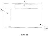
Fig. 15 is a top view of a detection device provided in an embodiment of the present disclosure. - The embodiments of the present disclosure will be described in further detail with reference to the accompanying drawings, to clearly present the objects, technical solutions, and advantages of the present disclosure.
- In related arts, as forming a plurality of data lines and a plurality of gate lines in an AMOLED display panel is difficult, many undesirable phenomena such as a short circuit and an open circuit may exist in the gate lines and the data lines, resulting in a defect in a produced AMOLED display panel. In order to improve a product yield of the AMOLED display panel, it is required to detect the AMOLED display panel.
- However, when detecting an AMOLED display panel in the prior art, only a defect in the data line can be detected (that is, a faulty data line can be detected), but a defect in the gate line cannot be detected (that is, a faulty gate line cannot be detected).
- An embodiment of the present disclosure provides a display panel. As shown in
Fig. 1, Fig. 1 is a schematic view of a structure of a display panel provided in an embodiment of the present disclosure. Thedisplay panel 10 may comprise a plurality ofdata lines 11 and a plurality ofgate lines 12, the plurality ofdata lines 11 and the plurality ofgate lines 12 intersect to form a plurality ofpixel units 13 in an enclosing manner; at least a part of thepixel units 13 may comprise a driving circuit and a pixel electrode; and the driving circuit is connected to a data line, a gate line and a power source end, respectively. For example, referring toFig. 2, Fig. 2 is a schematic view of a structure of a driving circuit provided in an embodiment of the present disclosure. The driving circuit may comprise: a first transistor T1, a second transistor T2 and a pixel storage capacitor Cst. - A gate electrode of the first transistor T1 is connected to the gate line; a first electrode of the first transistor T1 is connected to the data line; and a second electrode of the first transistor T1 and a gate electrode of the second transistor T2 are connected to a first metal layer of the pixel storage capacitor Cst.
- A first electrode of the second transistor T2 is connected to a power source end VDD; and a second electrode of the second transistor T2 is connected to a second metal layer of the pixel storage capacitor Cst and a pixel electrode ITO.
- In the embodiments of the present disclosure, in order to distinguish two electrodes of the transistor in addition to the gate electrode, a source electrode in the transistor may be referred to as a first electrode, and a drain electrode in the transistor may be referred to as a second electrode. Alternatively, the drain electrode in the transistor may be referred to as the first electrode, and the source electrode in the transistor may be referred to as the second electrode. The following embodiments are schematically illustrated by referring to the source electrode in the transistor as the first electrode and the drain electrode as the second electrode. A switching transistor used in the embodiments of the present disclosure may be an N-type switching transistor; and the N-type switching transistor is turned on when the gate electrode is at a high level, and is turned off when the gate electrode is at a low level. Moreover, a plurality of signals in various embodiments of the present disclosure each corresponds to a first level and a second level. The first level and the second level only represent two state quantities of the level of this signal, rather than a specific value of the first level or the second level.
- In some embodiments, a gate insulating layer is arranged between a source-drain electrode pattern and a gate electrode pattern in the display panel. When manufacturing the display panel, the gate insulating layer may not completely insulate the source-drain electrode pattern and the gate electrode pattern due to a process error. As a result, the source-drain electrode pattern is in contact with the gate electrode pattern, causing a short circuit between the gate line and the data line. In order to improve the product yield of the display panel, it is required to detect the display panel. When detecting the display panel provided in the embodiments of the present disclosure, it is required to mount the display panel on a detection device. For example, referring to
Fig. 3, Fig. 3 is a schematic view of an effect of a display panel mounted on a detection device provided in the embodiment of the present disclosure. The detection device may comprise a first signal input component A1 and a second signal input component A2. The plurality ofdata lines 11 in thedisplay panel 10 are connected to the same data input end; and the data input end is connected to the first signal input component A1. The plurality ofgate lines 12 in thedisplay panel 10 are connected to the same gate electrode scan input end; and the gate electrode scan input end is connected to the second signal input component A2. The first signal input component A1 is configured to simultaneously input a first data signal to the plurality of data lines through the data input end, or simultaneously input a second data signal to the plurality of data lines through the data input end. The second signal input component A2 is configured to simultaneously input a first gate line scan signal to the plurality of gate lines through the gate electrode scan input end, or simultaneously input a second gate line scan signal to the plurality of gate lines through the gate electrode scan input end. - Therefore, in a detection process of a display panel provided in the embodiments of the present disclosure, a driving circuit in each pixel unit may be connected to a data input end D, a gate electrode scan input end G1 and a power source end VDD, respectively.
- An embodiment of the present disclosure provides a detection method for a display panel. As shown in
Fig. 4, Fig. 4 is a flow chart of the detection method for the display panel provided in an embodiment of the present disclosure. The method is configured to detect the display panel shown inFig. 1 , and determine a short-circuited gate line in the display panel. The method may comprise the following steps. - In
step 101, a second data signal, a second gate line scan signal and a power source signal are input to a data input end, a gate electrode scan input end and a power source end, respectively. In the signal input process, the second data signal is at a first level; a level of the second gate line scan signal jumps from the first level to a second level; a level of the power source signal jumps from the first level to the second level; and the level of the second gate line scan signal jumps before the jumping of the level of the power source signal. - In
step 102, a second voltage of a pixel electrode in each pixel unit of the display panel is measured. - In
step 103, a faulty gate line is determined in accordance with the second voltage. - In summary, in the detection method for the display panel provided in the embodiments of the present disclosure, the second data signal, the second gate line scan signal and the power source signal are input to the data input end, the gate electrode scan input end and the power source end, respectively; the second voltage of the pixel electrode in each pixel unit of the display panel is measured; and the faulty gate line is determined in accordance with the second voltage.
- In the related art, as a faulty gate line cannot be detected, a position of a defective point in the AMOLED display panel cannot be located. Herein, the position of the defective point is a position where the faulty gate line intersects with a faulty data line. As a result, the gate line and the data line that correspond to the defective point cannot be repaired. Therefore, the current AMOLED display panel has a relatively lower product yield.
- In the embodiments of the present disclosure, the method may further comprise: detecting a faulty data line; and determining a position of a defective point in the display panel according to a faulty gate line and the faulty data line. The defective point is a short-circuited defective point. When the gate line and the data line are short-circuited, the position where the gate line is connected to the data line is the position of the defective point.
- For example, as shown in
Fig. 5, Fig. 5 is a flow chart of a detection method for another display panel provided in an embodiment of the present disclosure. The method is configured to detect the display panel shown inFig. 1 , and determine a short-circuited gate line and a short-circuited data line in the display panel. The method may comprise the following steps. - In
step 201, a first data signal, a first gate line scan signal and a power source signal are input to a data input end, a gate electrode scan input end and a power source end, respectively. In a signal input process, the first gate line scan signal is at a first level; a level of the first data signal jumps from the first level to a second level; a level of the power source signal jumps from the first level to the second level; and the level of the first data signal jumps before the jumping of the level of the power source signal. - In
step 202, a first voltage of a pixel electrode in each pixel unit of the display panel is measured. - In
step 203, a faulty data line is determined in accordance with the first voltage. - In
step 204, a second data signal, a second gate line scan signal and a power source signal are input to the data input end, the gate electrode scan input end and the power source end, respectively. In the signal input process, the second data signal is at the first level; a level of the second gate line scan signal jumps from the first level to the second level; a level of the power source signal jumps from the first level to the second level; and the level of the second gate line scan signal jumps before the jumping of the level of the power source signal. - In
step 205, a second voltage of the pixel electrode in each pixel unit of the display panel is measured. - In
step 206, a faulty gate line is determined in accordance with the second voltage. - In
step 207, a position of a defective point in the display panel is determined in accordance with the faulty gate line and the faulty data line. - In summary, in the detection method for the display panel provided in the embodiments of the present disclosure, the first data signal, the first gate line scan signal and the power source signal are input to the data input end, the gate electrode scan input end and the power source end, respectively; the first voltage of the pixel electrode in each pixel unit of the display panel is measured; the faulty data line is determined in accordance with the first voltage; the second data signal, the second gate line scan signal and the power source signal are input to the data input end, the gate electrode scan input end and the power source end, respectively; the second voltage of the pixel electrode in each pixel unit of the display panel is measured; and the faulty gate line is determined in accordance with the second voltage. Further, the position of the defective point in the display panel is determined in accordance with the faulty gate line and the faulty data line. When the position of the defective point in the display panel is determined, the gate line and the data line that correspond to the defective point can be repaired, so that the product yield of the display panel can be improved.
- In the embodiments of the present disclosure, different signals are input to the plurality of data lines through the first signal input component, and different signals are input to the plurality of gate lines through the second signal input component, so that the faulty data line and the faulty gate line can be determined. In the embodiments of the present disclosure, as the manner for determining the faulty data line is different from that for determining the faulty gate line, the embodiment of the present disclosure is schematically illustrated in the following two aspects.
- In a first aspect, when it is required to determine a faulty data line, referring to
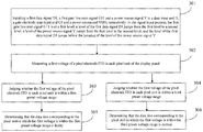
Fig. 6 which is a timing sequence diagram of each signal end in a detection process provided in an embodiment of the present disclosure, a first detection component transmits a first data signal D1 to a data input end D; and a second detection component transmits a first gate line scan signal G11 to a gate electrode scan input end G1. Referring toFig. 7, Fig. 7 is a flow chart of a detection method for another display panel provided in an embodiment of the present disclosure. The method is configured to detect the display panel shown inFig. 1 , and determine a short-circuited data line in the display panel. The method may comprise the following steps. - In
step 301, a first data signal D1, a first gate line scan signal G11 and a power source signal V are input to a data input end D, a gate electrode scan input end G1 and a power source end VDD, respectively. In the signal input process, the first gate line scan signal G11 is at a first level; a level of the first data signal D1 jumps from the first level to a second level; a level of the power source signal V jumps from the first level to the second level; and the level of the first data signal D1 jumps before the jumping of the level of the power source signal V. - For example, as shown in
Fig. 6 , the method in thestep 301 may be divided into three stages, namely, t1, t2 and t3. In the first stage t1, all the first gate line scan signal G11, the first data signal D1 and the power source signal V are at the first level; in the second stage t2, the first gate line scan signal G11 and the power source signal V are at the first level, and the first data signal D1 is at the second level; and in the third stage t3, the first gate line scan signal G11 is at the first level, and both the first data signal D1 and the power source signal V are at the second level. - Herein, when the first gate line scan signal G11 is at the first level, the voltage value may be 20 volts; when the first data signal D1 is at the first level, the voltage value may be 25 volts; when the first data signal D1 is at the second level, the voltage value may be -8 volts; when the power source signal V is at the first level, the voltage value may be 25 volts; and when the power source signal V is at the second level, the voltage value may be -15 volts.
- In the embodiments of the present disclosure, as shown in
Figs. 2 and6 , the level of the first gate line scan signal G11 input by the second signal input component to the gate electrode scan input end G1 does not jump during a detection process, and is always at the first level, so that the first transistor T1 is always in a turn-on state during the signal input process. When the gate line and the data line are both normal (that is, both the gate line and the data line can perform effective data transmission without failure such as short circuit, open circuit or others), if the first data signal D1 input from the data input end D is at the first level, the second transistor T2 is in a turn-on state; or if the first data signal D1 is at the second level, the second transistor T2 is in a turn-off state. When the gate line and the data line are short-circuited, a potential of the first data signal D1 transmitted on the data line is affected by the first gate line scan signal G11 transmitted on the gate line. As a result, when the first data signal D1 input by the data input end D is at the second level, the voltage on the data line is pulled up by the first gate line scan signal G11 transmitted on the gate line, so that the on-off state of the second transistor T2 is unaffected by the level of the first data signal D1, and the second transistor T2 is always in the turn-on state. - In
step 302, a first voltage of a pixel electrode ITO in each pixel unit of the display panel is measured. - In the embodiments of the present disclosure, as shown in
Figs. 2 and6 , as the level of the first data signal D1 jumps before the jumping of the level of the power source signal V, if the gate line and the data line are both normal, it is detected that the first voltage of the pixel electrode ITO is always the voltage when the power source signal V is at the first level; or if the gate line and the data line are short-circuited, it can be detected that the first voltage of the pixel electrode ITO is the voltage when the power source signal V is at the second level. - For example, when both the gate line and the data line are normal, the second transistor T2 may be in a turn-on state or in a turn-off state under the control of the first data signal D1. For instance, when the second transistor T2 is in the turn-on state, the power source end VDD can charge the pixel storage capacitor Cst, so that both the voltages at the two ends of the storage capacitor Cst are the voltage when the power source signal V is at the first level, and it can be measured that the first voltage of the pixel electrode ITO is the voltage when the power source signal V is at the first level. When the second transistor T2 is in the turn-off state, the pixel storage capacitor Cst is not discharged or charged, the voltage of the pixel electrode ITO is the voltage at one end of the storage capacitor Cst, and it can be measured that the first voltage of the pixel electrode ITO is also the voltage when the power source signal V is at the first level.
- When the gate line and the data line are short-circuited, as the second transistor T2 is always in the turn-on state under the influence of the first gate line scan signal G11 transmitted on the gate line, it can be measured that the first voltage of the pixel electrode ITO is the voltage when the power source signal V is at the second level.
- For example, referring to
Fig. 8, Fig. 8 is a diagram of an analogue simulation of a first voltage which measures a pixel electrode ITO provided in an embodiment of the present disclosure. When both the gate line and the data line are normal, the first voltage of the pixel electrode ITO is always the voltage when the power source signal V is at the first level, and finally, it can be detected that the first voltage of the pixel electrode ITO is 25 volts. When the gate line and the data line are short-circuited, the first voltage of the pixel electrode ITO drops to the voltage when the power source signal V is at the second level, and finally, it can be detected that the first voltage of the pixel electrode ITO is -15 volts. - Therefore, in the embodiments of the present disclosure, the first voltage of the pixel electrode ITO in each pixel unit of the display panel can be measured, and thus a short-circuited data line in the display panel can be judged.
- In
step 303, it is judged whether the first voltage of the pixel electrode ITO in each pixel unit is within a first preset voltage range. - Herein, a lower limit value in the first preset voltage range is greater than or equal to the voltage value when the power source signal V is at the second level.
- In some embodiments, as shown in
Fig. 2 , there may be resistance in the second transistor T2, so that when the gate line and the data line are short-circuited and after the power source signal V input in the power source end VDD is transmitted to the pixel electrode ITO, the voltage when the power source signal V is at the second level is divided by the resistance in the second transistor T2, causing the first voltage of the pixel electrode ITO to be possibly greater than the voltage when the power source signal V is at the second level. Thus, when it is judged that the first voltage of the pixel electrode ITO in each pixel unit is within the first preset voltage range,step 305 is executed. - In
step 304, it is judged whether the first voltage of the pixel electrode ITO in each pixel unit is within a third preset voltage range. - Herein, a lower limit value in the third preset voltage range is greater than an upper limit value in the first preset voltage range.
- In some embodiments, as shown in
Fig. 2 , similarly, when both the gate line and the data line are normal, the first voltage of the pixel electrode ITO may be lower than the voltage when the power source signal V is at the first level, thus when it is judged that the first voltage of the pixel electrode ITO in each pixel unit is within the third preset voltage range,step 306 is executed. - In
step 305, it is determined that the data line corresponding to the pixel unit in which the first voltage is within the first preset voltage range is faulty. - In the embodiments of the present disclosure, the data line corresponding to the pixel unit refers to the data line connected to a driving circuit in the pixel unit.
- In
step 306, it is determined that the data line corresponding to the pixel unit in which the first voltage is within the third preset voltage range is normal. - It should be noted that when the first voltage is neither within the first preset voltage range nor within the third preset range, other faults may appear in the display panel.
- It should be noted that in the embodiments of the present disclosure, after executing the
above step 302,step 303 may be executed first, and then step 304 is executed; or,steps - In the second aspect, when it is required to determine a faulty gate line, referring to
Fig. 9 which is a timing sequence diagram of each signal end in another detection process provided in an embodiment of the present disclosure, a first detection component transmits a second data signal D2 to a data input end D; and a second detection component transmits a second gate line scan signal G12 to a gate electrode scan input end G1. Referring toFig. 10, Fig. 10 is a flow chart of a detection method for yet another display panel provided in the embodiment of the present disclosure. The method is configured to detect the display panel shown inFig. 1 , and determine a short-circuited gate line in the display panel. The method may comprise the following steps. - In
step 401, a second data signal D2, a second gate line scan signal G12 and a power source signal V are respectively input to the data input end D, the gate electrode scan input end G1 and the power source end VDD. In the signal input process, the second data signal D2 is at a first level; a level of the second gate line scan signal G12 jumps from the first level to a second level; a level of the power source signal V jumps from the first level to the second level; and the level of the second gate line scan signal G12 jumps before the jumping of the level of the power source signal V. - For example, as shown in
Fig. 9 , the method illustrated instep 401 may be divided into three stages, namely, t1, t2 and t3. In the first stage t1, all the second gate line scan signal G12, the second data signal D2 and the power source signal V are at the first level; in the second stage t2, both the second data signal D2 and the power source signal V are at the first level, and the second gate line scan signal G12 is at the second level; and in the third stage t3, the second data signal D2 is at the first level, both the second gate line scan signal G12 and the power source signal V are at the second level. - Herein, when the second data signal D2 is at the first level, the voltage value may be 8 volts; when the second gate line scan signal G12 is at the first level, the voltage value may be 25 volts; and when the second gate line scan signal G12 is at the second level, the voltage value may be -25 volts.
- In the embodiments of the present disclosure, as shown in
Figs. 2 and9 , in a signal transmission process, when both the gate line and the data line are normal, if the second gate line scan signal G12 input from the gate electrode scan input end G1 is at the first level, the first transistor T1 is in a turn-on state; or if the second gate line scan signal G12 input from the gate electrode scan input end G1 is at the second level, the first transistor T1 is in a turn-off state. In a detection process, the level of the second data signal D2 input by the first signal input component to the data input end D does not jump, and is always at the first level, so that when the first transistor T1 is in the turn-on state, the second transistor T2 is also in the turn-on state; and when the first transistor T1 is in the turn-off state, the second transistor T2 is also in the turn-off state. When the gate line and the data line are short-circuited, a potential of the second gate line scan signal G12 transmitted on the gate line is affected by the second data signal D2 transmitted on the data line. As a result, when the second gate line scan signal G12 input from the gate electrode scan input end G1 is at the second level, the voltage on the gate line is pulled up by the second data signal D2 transmitted on the data line, so that the on-off state of the first transistor T1 is unaffected by the level of the second gate line scan signal G12, and the first transistor T1 is always in the turn-on state. In addition, as the level of the second data signal D2 input from the data input end D does not jump, and is always at the first level, the second transistor T2 is always in the turn-on state in a signal input process. - In
step 402, a second voltage of a pixel electrode ITO in each pixel unit of the display panel is measured. - In the embodiments of the present disclosure, as shown in
Figs. 2 and9 , as the level of the second gate line scan signal G12 jumps before the jumping of the level of the power source signal V, if the gate line and the data line are both normal, it can be detected that the second voltage of the pixel electrode ITO is not the voltage when the power source signal V is at the second level; or if the gate line and the data line are short-circuited, it can be detected that the second voltage of the pixel electrode ITO is the voltage when the power source signal V is at the second level. - For example, when both the gate line and the data line are normal, the first transistor T1 may be in a turn-on state or in a turn-off state under the control of the second gate line scan signal G12. For instance, when the first transistor T1 is in the turn-on state, the second transistor T2 is also in the turn-on state, and the voltage end VDD can charge the pixel storage capacitor Cst, so that the voltages at the two ends of the storage capacitor Cst are the voltage when the power source signal V is at the first level, and it can be measured that the second voltage of the pixel electrode ITO is the voltage when the power source signal V is at the first level. When the first transistor T1 is in the turn-off state, the pixel storage capacitor Cst is discharged, so that the second transistor T2 cannot be turned off immediately. After the discharging of the pixel storage capacitor Cst is completed, the second transistor T2 is in the turn-off state. During the discharging process of the capacitor Cst, the voltages at the two ends of the storage capacitor Cst drop continuously, so that the voltage of the pixel electrode ITO continues to drop, and the second voltage of the pixel electrode ITO stops to drop until the second transistor T2 is in the turn-off state.
- When the gate line and the data line are short-circuited, as the first transistor T1 is always in a turn-on state under the influence of the second data signal D2 transmitted on the data line, the second transistor T2 is always in the turn-on state; and at this time, it can be measured that the second voltage of the pixel electrode ITO is the voltage when the power source signal V is at the second level.
- For example, referring to
Fig. 11, Fig. 11 is a diagram of an analogue simulation of a second voltage for measuring a pixel electrode ITO provided in an embodiment of the present disclosure. When both the gate line and the data line are normal, after the second voltage of the pixel electrode ITO drops to -2.5743 volts, the second transistor T2 is turned off, and finally, it can be measured that the second voltage of the pixel electrode ITO is -2.5743 volts. When the gate line and the data line are short-circuited, the second voltage of the pixel electrode ITO drops to the voltage when the power source signal V is at the second level, and finally, it can be measured that the second voltage of the pixel electrode ITO is -15 volts. - Therefore, in the embodiments of the present disclosure, the second voltage of the pixel electrode ITO in each pixel unit of the display panel can be measured, and thus a short-circuited gate line in the display panel can be judged.
- In
step 403, it is judged whether the second voltage of the pixel electrode ITO in each pixel unit is within a second preset voltage range. - Herein, a lower limit value in the second preset voltage range is greater than or equal to the voltage value when the power source signal V is at the second level.
- In some embodiments, as shown in
Fig. 2 , there may be resistance in the second transistor T2, so that when the gate line and the data line are short-circuited and after the power source signal V input from the power source end VDD is transmitted to the pixel electrode ITO, the voltage when the power source signal V is at the second level is divided by the resistance in the second transistor T2, causing the second voltage of the pixel electrode ITO to be possibly greater than the voltage when the power source signal V is at the second level. As a result, when it is judged that the second voltage of the pixel electrode ITO in each pixel unit is within the second preset voltage range,step 405 is executed. - It should be noted that the first preset voltage range and the second preset voltage range provided in the embodiments of the present disclosure are the same. That is, values included in the first preset voltage range are the same as those included in the second preset voltage range.
- In
step 404, it is judged whether the second voltage of the pixel electrode ITO in each pixel unit is within a fourth preset voltage range. - Herein, a lower limit value in the fourth preset voltage range is greater than an upper limit value in the second preset voltage range.
- For example, when it is judged that the second voltage of the pixel electrode ITO in each pixel unit is within the fourth preset voltage range,
step 406 is executed. - In
step 405, it is determined that the gate line corresponding to the pixel unit in which the second voltage is within the second preset voltage range is faulty. - In the embodiments of the present disclosure, the gate line corresponding to the pixel unit refers to the gate line connected to the driving circuit in the pixel unit.
- In
step 406, it is determined that the gate line corresponding to the pixel unit in which the second voltage is within the fourth preset voltage range is normal. - It should be noted that when the second voltage is neither within the second preset voltage range nor within the fourth preset range, other faults may appear in the display panel.
- It should be noted that in the embodiments of the present disclosure, after executing the
above step 402,step 403 may be executed first, and then step 404 is executed; or,steps - It should be noted that after
step 305 and step 405 in the above embodiments, the faulty gate line and the faulty data line can be determined; and a position of a defective point in the display panel can be determined in accordance with the faulty gate line and the faulty data line, so that the gate line and the data line corresponding to the defective point can be repaired, thereby improving the product yield of the display panel. - It should be noted that a sequence of the steps of the detection method for the display panel provided by the embodiments of the present disclosure may be appropriately adjusted, and the steps may also be correspondingly increased or decreased in accordance with a situation. For example, the faulty gate line may be determined first, and then the faulty data line may be determined. That is, the steps in
Fig. 10 are executed first, and then the steps inFig. 7 are executed. Any variation methods which can be easily expected by any person skilled in the art within the technical scope disclosed by the present disclosure should be covered in the protection scope of the present disclosure, which is not repeated herein. - In summary, in the detection method for the display panel provided in the embodiments of the present disclosure, the first data signal, the first gate line scan signal and the power source signal are input to the data input end, the gate electrode scan input end and the power source end, respectively; the first voltage of the pixel electrode in each pixel unit of the display panel is measured; the faulty data line is determined in accordance with the first voltage; the second data signal, the second gate line scan signal and the power source signal are input to the data input end, the gate electrode scan input end and the power source end, respectively; the second voltage of the pixel electrode in each pixel unit of the display panel is measured; and the faulty gate line is determined in accordance with the second voltage. Further, the position of the defective point in the display panel is determined in accordance with the faulty gate line and the faulty data line. When the position of the defective point in the display panel is determined, the gate line and the data line that correspond to the defective point can be repaired, so that the product yield of the display panel can be improved.An embodiment of the present disclosure further provides a detection apparatus for a display panel. The display panel may comprise a plurality of data lines and a plurality of gate lines which intersect to form a plurality of pixel units in an enclosing manner; at least a part of the pixel units comprises a driving circuit and a pixel electrode; and the driving circuit is connected to a data input end, a gate electrode scan input end and a power source end, respectively. The detection apparatus for the display panel may comprise:
- a second input module configured to input a second data signal, a second gate line scan signal and a power source signal to the data input end, the gate electrode scan input end and the power source end, respectively, wherein in the signal input process, the second data signal is at a first level; a level of the second gate line scan signal jumps from the first level to a second level; a level of the power source signal jumps from the first level to the second level; the level of the second gate line scan signal jumps before the jumping of the level of the power source signal;
- a second measurement module configured to measure a second voltage of a pixel electrode in each pixel unit of the display panel; and
- a second determination module configured to determine a faulty gate line in accordance with the second voltage.Optionally, the detection apparatus for the display panel may comprise a first determination module configured to determine a faulty data line, and
- a third determination module configured to determine a position of a defective point in the display panel in accordance with the faulty gate line and the faulty data line. Optionally, the defective point is a short-circuited defective point.
- For example, referring to
Fig. 12, Fig. 12 is a block diagram of a detection apparatus for a display panel provided in an embodiment of the present disclosure. The detection apparatus 50 for the display panel may comprise: - a
first input module 501 configured to input a first data signal, a first gate line scan signal and a power source signal to a data input end, a gate electrode scan input end and a power source end, respectively, wherein in a signal input process, the first gate line scan signal is at a first level; a level of the first data signal jumps from the first level to a second level; a level of the power source signal jumps from the first level to the second level; and the level of the first data signal jumps before the jumping of the level of the power source signal; - a
first measurement module 502 configured to measure a first voltage of a pixel electrode in each pixel unit of the display panel; - a
first determination module 503 configured to determine a faulty data line in accordance with the first voltage; - a
second input module 504 configured to input a second data signal, a second gate line scan signal and a power source signal to the data input end, the gate electrode scan input end and the power source end, respectively, wherein in the signal input process, the second data signal is at a first level; a level of the second gate line scan signal jumps from the first level to a second level; a level of the power source signal jumps from the first level to the second level; and the level of the second gate line scan signal jumps before the jumping of the level of the power source signal; - a
second measurement module 505 configured to measure a second voltage of a pixel electrode in each pixel unit of the display panel; - a
second determination module 506 configured to determine a faulty gate line in accordance with the second voltage; and - a
third determination module 507 configured to determine a position of a defective point in the display panel in accordance with the faulty gate line and the faulty data line. - In summary, in the detection apparatus for the display panel provided in the embodiments of the present disclosure, the first data signal, the first gate line scan signal and the power source signal are input to the data input end, the gate electrode scan input end and the power source end, respectively; the first voltage of the pixel electrode in each pixel unit of the display panel is measured; the faulty data line is determined in accordance with the first voltage; the second data signal, the second gate line scan signal and the power source signal are input to the data input end, the gate electrode scan input end and the power source end, respectively; the second voltage of the pixel electrode in each pixel unit of the display panel is measured; and the faulty gate line is determined in accordance with the second voltage. Further, the position of the defective point in the display panel is determined in accordance with the faulty gate line and the faulty data line. When the position of the defective point in the display panel is determined, the gate line and the data line corresponding to the defective point can be repaired, so that the product yield of the display panel can be improved.
- Optionally, the
first determination module 503 is configured to - judged whether the first voltage of the pixel electrode in each pixel unit is within a first preset voltage range, and determine that the data line corresponding to the pixel unit in which the first voltage is within the first preset voltage range is faulty, wherein a lower limit value of the first preset voltage range is greater than or equal to a voltage value when the power source signal is at the second level.
- Optionally, the
second determination module 506 is configured to
judged whether the second voltage of the pixel electrode in each pixel unit is within a second preset voltage range, and determine that the gate line corresponding to the pixel unit in which the second voltage is within the second preset voltage range is faulty, wherein a lower limit value of the second preset voltage range is greater than or equal to a voltage value when the power source signal is at the second level. - Optionally, referring to
Fig. 13, Fig. 13 is a block diagram of a detection apparatus for another display panel in accordance with an embodiment of the present disclosure. Thedetection apparatus 500 for the display panel may further comprise: - a
first judgment module 508 configured to judge whether the first voltage of the pixel electrode in each pixel unit is within a third preset voltage range; and - a
fourth determination module 509 configured to determine that the data line corresponding to the pixel unit in which the first voltage is within the third preset voltage range is normal. - Herein, a lower limit value in the third preset voltage range is greater than an upper limit value in the first preset voltage range.
- Optionally, referring to
Fig. 14, Fig. 14 is a block diagram of a detection apparatus for yet another display panel provided in an embodiment of the present disclosure. Thedetection apparatus 500 for the display panel may further comprise: - a
second judgment module 510 configured to judge whether the second voltage of the pixel electrode in each pixel unit is within a fourth preset voltage range; and - a
fifth determination module 511 configured to determine that the gate line corresponding to the pixel unit in which the second voltage is in the fourth preset voltage range is normal. Herein, a lower limit value in the fourth preset voltage range is greater than an upper limit value in the second preset voltage range.In some embodiments, when the first gate line scan signal is at the first level, the voltage value is 20 volts; when the first data signal is at the first level, the voltage value is 25 volts; when the first data signal is at the second level, the voltage value is -8 volts; when the power source signal is at the first level, the voltage value is 25 volts; when the power source signal is at the second level, the voltage value is -15 volts; when the second data signal is at the first level, the voltage value is 8 volts; when the second gate line scan signal is at the first level, the voltage value is 25 volts; and when the second gate line scan signal is at the second level, the voltage value is -25 volts. - A person skilled in the art can easily understand that for the sake of convent and brief description, a particular working process of the above apparatus can refer to a corresponding process in the foregoing method embodiments, and details are not repeated herein.
- In summary, in the detection apparatus for the display panel provided in the embodiments of the present disclosure, the first data signal, the first gate line scan signal and the power source signal are input to the data input end, the gate electrode scan input end and the power source end, respectively; the first voltage of the pixel electrode in each pixel unit of the display panel is measured; the faulty data line is determined in accordance with the first voltage; the second data signal, the second gate line scan signal and the power source signal are input to the data input end, the gate electrode scan input end and the power source end, respectively; the second voltage of the pixel electrode in each pixel unit of the display panel is measured; and the faulty gate line is determined in accordance with the second voltage. Further, the position of the defective point in the display panel is determined in accordance with the faulty gate line and the faulty data line. When the position of the defective point in the display panel is determined, the gate line and the data line corresponding to the defective point can be repaired, so that the product yield of the display panel can be improved.
- An embodiment of the present disclosure further provides a detection device for detecting a display panel shown in
Fig. 1 . The detection device comprises: - a processor; and
- a memory.
- The memory stores one or more programs which are configured to be executed by the processor. The one or more programs include a detection method for a display panel according to the
above steps 101 to 103, or include a detection method for a display panel according to theabove steps 201 to 207, or a detection method for a display panel according to theabove steps 301 to 306, or a detection method for a display panel according to theabove steps 401 to 406. - Optionally, as shown in
Fig. 15, Fig. 15 is a top view of a detection device provided in an embodiment of the present disclosure. The detection device may comprise abearing base 150, a first signal input component A1 and a second signal input component A2. The first signal input component A1 and the second signal input component A2 are both arranged on thebearing base 150. When it is required to detect the display panel, the display panel may be arranged on thebearing base 150, and a plurality of data lines in the display panel are connected to the first signal input component A1; and a plurality of gate lines in the display panel are connected to the second signal input component A2. A connection relationship between the detection device and the display panel may refer toFig. 3 . - It should be noted that the processor in the detection device may be connected to the first signal input component A1 and the second signal input component A2; or the processor and the memory may be simultaneously arranged in each of the first signal input component A1 and the second signal input component A2. Thus, the first signal input component can input a first data signal to each of the plurality of data lines or can input a second data signal to each of the plurality of data lines; and the second signal input component can input a first gate electrode scan signal to each of the plurality of gate lines or input a second gate electrode scan signal to each of the plurality of gate lines.
- In an exemplary embodiment, there is also provided a non-volatile computer-readable storage medium comprising instructions, such as a memory comprising the instructions executable by a processor in a detection device to perform the detection method for the display panel described in the
above steps 101 to 103, or the detection method for the display panel described in theabove steps 201 to 207, or the detection method for the display panel described in theabove steps 301 to 306, or the detection method for the display panel described in theabove steps 401 to 406. For example, the non-volatile computer-readable storage medium may be an ROM, a random access memory (RAM), a CD-ROM, a magnetic tape, a floppy disk, an optical data storage device, or the like. - In an exemplary embodiment, there is also provided a computer program product in which instructions are stored. When the instructions are run on the computer, the computer can execute the detection method for the display panel described in the
above steps 101 to 103, or the detection method for the display panel described in theabove steps 201 to 207, or the detection method for the display panel described in theabove steps 301 to 306, or the detection method for the display panel described in theabove steps 401 to 406. - In an exemplary embodiment, there is also provided a chip comprising a programmable logic circuit and/or program instructions. When running, the chip is configured to realize the detection method for the display panel described in the
above steps 101 to 103, or the detection method for the display panel described in theabove steps 201 to 207, or the detection method for the display panel described in theabove steps 301 to 306, or the detection method for the display panel described in theabove steps 401 to 406. - Persons of ordinary skill in the art can understand that all or part of the steps described in the above embodiments can be completed through hardware, or through relevant hardware instructed by programs that may be stored in a non-transitory computer readable storage medium, such as read-only memory, disk or CD, etc.
- The foregoing descriptions are only preferred embodiments of the present disclosure, and are not intended to limit the present disclosure. Within the spirit and principles of the disclosure, any modifications, equivalent substitutions, improvements, etc., are within the protection scope of the present disclosure.
Claims (20)
- A detection method for a display panel, wherein the display panel comprises a plurality of data lines and a plurality of gate lines; the plurality of data lines and the plurality of gate lines intersect to form a plurality of pixel units in an enclosing manner; at least a part of the pixel units comprises a driving circuit and a pixel electrode; the driving circuit is connected to a data input end, a gate electrode scan input end and a power source end, respectively; and the method comprises:inputting a second data signal, a second gate line scan signal and a power source signal respectively to the data input end, the gate electrode scan input end and the power source end, wherein during the signal inputting process, the second data signal is at a first level, a level of the second gate line scan signal jumps from the first level to a second level, a level of the power source signal jumps from the first level to the second level, and the level of the second gate line scan signal jumps before the jumping of the level of the power source signal;measuring a second voltage of the pixel electrode in each pixel unit of the display panel; anddetermining a faulty gate line according to the second voltage.
- The method of claim 1, further comprising:determining a faulty data line; anddetermining a position of a defective point in the display panel according to the faulty gate line and the faulty data line.
- The method of claim 2, wherein the defective point is a short-circuited defective point; and determining the faulty data line comprises:inputting a first data signal, a first gate line scan signal and a power source signal respectively to the data input end, the gate electrode scan input end and the power source end, wherein during the signal inputting process, the first gate line scan signal is at the first level, a level of the first data signal jumps from the first level to the second level, a level of the power source signal jumps from the first level to the second level, and the level of the first data signal jumps before the jumping of the level of the power source signal;measuring a first voltage of the pixel electrode in each pixel unit of the display panel; anddetermining the faulty data line according to the first voltage.
- The method of claim 3, wherein determining the faulty data line according to the first voltage comprises:judging whether the first voltage of the pixel electrode in each pixel unit is within a first preset voltage range; anddetermining that the data line corresponding to the pixel unit in which the first voltage is within the first preset voltage range is faulty, wherein a lower limit value in the first preset voltage range is greater than or equal to a voltage value when the power source signal is at the second level.
- The method of claim 3, wherein determining the faulty gate line according to the second voltage comprises:judging whether the second voltage of the pixel electrode in each pixel unit is within a second preset voltage range; anddetermining that the gate line corresponding to the pixel unit in which the second voltage is within the second preset voltage range is faulty,wherein a lower limit value in the second preset voltage range is greater than or equal to a voltage value when the power source signal is at the second level.
- The method of claim 4, wherein after measuring the first voltage of the pixel electrode in each pixel unit of the display panel, the method further comprises:judging whether the first voltage of the pixel electrode in each pixel unit is within a third preset voltage range; anddetermining that the data line corresponding to the pixel unit in which the first voltage is within the third preset voltage range is normal,wherein a lower limit value in the third preset voltage range is greater than an upper limit value in the first preset voltage range.
- The method of claim 5, wherein after measuring the second voltage of the pixel electrode in each pixel unit of the display panel, the method further comprises:judging whether the second voltage of the pixel electrode in each pixel unit is within a fourth preset voltage range; anddetermining that the gate line corresponding to the pixel unit in which the second voltage is within the fourth preset voltage range is normal,wherein a lower limit value in the fourth preset voltage range is greater than an upper limit value in the second preset voltage range.
- The method of any one of claims 3-7, wherein,
when the first gate line scan signal is at the first level, the voltage value is 20 volts; when the first data signal is at the first level, the voltage value is 25 volts; when the first data signal is at the second level, the voltage value is -8 volts; when the power source signal is at the first level, the voltage value is 25 volts; and when the power source signal is at the second level, the voltage value is -15 volts; and
when the second data signal is at the first level, the voltage value is 8 volts; when the second gate line scan signal is at the first level, the voltage value is 25 volts; and when the second gate line scan signal is at the second level, the voltage value is -25 volts. - A detection apparatus for a display panel, wherein the display panel comprises a plurality of data lines and a plurality of gate lines; the plurality of data lines and the plurality of gate lines intersect to form a plurality of pixel units in an enclosing manner; at least a part of the pixel units comprises a driving circuit and a pixel electrode; the driving circuit is connected to a data input end, a gate electrode scan input end and a power source end, respectively; and the apparatus comprises:a second input module configured to input a second data signal, a second gate line scan signal and a power source signal respectively to the data input end, the gate electrode scan input end and the power source end, wherein during the signal inputting process, the second data signal is at a first level, a level of the second gate line scan signal jumps from the first level to a second level, a level of the power source signal jumps from the first level to the second level, and the level of the second gate line scan signal jumps before the jumping of the level of the power source signal;a second measurement module configured to measure a second voltage of a pixel electrode in each pixel unit of the display panel; anda second determination module configured to determine a faulty gate line according to the second voltage.
- The apparatus of claim 9, further comprising:a first determination module configured to determine a faulty data line; anda third determination module configured to determine a position of a defective point in the display panel according to the faulty gate line and the faulty data line.
- The apparatus of claim 10, wherein the defective point is a short-circuited defective point, and the apparatus further comprises:a first input module configured to input a first data signal, a first gate line scan signal and a power source signal respectively to the data input end, the gate electrode scan input end and the power source end, wherein during the signal inputting process, the first gate line scan signal is at the first level, a level of the first data signal jumps from the first level to the second level, a level of the power source signal jumps from the first level to the second level, and the level of the first data signal jumps before the jumping of the level of the power source signal;a first measurement module configured to measure a first voltage of the pixel electrode in each pixel unit of the display panel; andthe first determination module configured to determine a faulty data line according to the first voltage.
- The apparatus of claim 11, wherein the first determination module is configured to:judge whether the first voltage of the pixel electrode in each pixel unit is within a first preset voltage range, anddetermine that the data line corresponding to the pixel unit in which the first voltage is within the first preset voltage range is faulty,wherein a lower limit value in the first preset voltage range is greater than or equal to a voltage value when the power source signal is at the second level.
- The apparatus of claim 12, wherein the second determination module is configured to:judge whether the second voltage of the pixel electrode in each pixel unit is within a second preset voltage range; anddetermine that the gate line corresponding to the pixel unit in which the second voltage is within the second preset voltage range is faulty,wherein a lower limit value in the second preset voltage range is greater than or equal to a voltage value when the power source signal is at the second level.
- The apparatus of claim 12, further comprising:a first judgment module configured to judge whether the first voltage of the pixel electrode in each pixel unit is within a third preset voltage range; anda fourth determination module configured to determine that the data line corresponding to the pixel unit in which the first voltage is in the third preset voltage range is normal,wherein a lower limit value in the third preset voltage range is greater than an upper limit value in the first preset voltage range.
- The apparatus of claim 13, further comprising:a second judgment module configured to judge whether the second voltage of the pixel electrode in each pixel unit is within a fourth preset voltage range; anda fifth determination module configured to determine that the gate line corresponding to the pixel unit in which the second voltage is in the fourth preset voltage range is normal,wherein a lower limit value in the fourth preset voltage range is greater than an upper limit value in the second preset voltage range.
- The apparatus of any one of claims 9-15, wherein,
when the first gate line scan signal is at the first level, the voltage value is 20 volts; when the first data signal is at the first level, the voltage value is 25 volts; when the first data signal is at the second level, the voltage value is -8 volts; when the power source signal is at the first level, the voltage value is 25 volts; when the power source signal is at the second level, the voltage value is -15 volts; and
when the second data signal is at the first level, the voltage value is 8 volts; when the second gate line scan signal is at the first level, the voltage value is 25 volts; and when the second gate line scan signal is at the second level, the voltage value is -25 volts. - A detection device for detecting a display panel, wherein the display panel comprises a plurality of data lines and a plurality of gate lines; the plurality of data lines and the plurality of gate lines intersect to form a plurality of pixel units in an enclosing manner; at least a part of the pixel units comprises a driving circuit and a pixel electrode; the driving circuit is connected to a data input end, a gate electrode scan input end and a power source end, respectively; and the detection device comprises:a processor, anda memory storing one or more programs executed by the processor, and the one or more programs comprises instructions for performing the following operations:inputting a second data signal, a second gate line scan signal and a power source signal respectively to the data input end, the gate electrode scan input end and the power source end, wherein during the signal inputting process, the second data signal is at a first level, a level of the second gate line scan signal jumps from the first level to a second level, a level of the power source signal jumps from the first level to the second level, and the level of the second gate line scan signal jumps before the jumping of the level of the power source signal;measuring a second voltage of the pixel electrode in each pixel unit of the display panel; anddetermining a faulty gate line according to the second voltage.
- The detection device of claim 17, wherein the one or more programs comprises instructions for performing the following operations:determining a faulty data line; anddetermining a position of a defective point in the display panel according to the faulty gate line and the faulty data line.
- The detection device of claim 18, wherein the defective point is a short-circuited defective point, and the one or more programs include instructions for performing the following operations:inputting a first data signal, a first gate line scan signal and a power source signal respectively to the data input end, the gate electrode scan input end and the power source end, wherein during the signal inputting process, the first gate line scan signal is at the first level, a level of the first data signal jumps from the first level to the second level, a level of the power source signal jumps from the first level to the second level, and the level of the first data signal jumps before the jumping of the level of the power source signal;measuring a first voltage of the pixel electrode in each pixel unit of the display panel; anddetermining the faulty data line according to the first voltage.
- A computer-readable storage medium storing a computer program, wherein the stored computer program is executed by a processor for implementing the detection method for the display panel according to any one of claims 1-8.
Applications Claiming Priority (2)
| Application Number | Priority Date | Filing Date | Title |
|---|---|---|---|
| CN201710672710.2A CN109389919B (en) | 2017-08-08 | 2017-08-08 | Display panel detection method and device |
| PCT/CN2018/099198 WO2019029532A1 (en) | 2017-08-08 | 2018-08-07 | Display panel detection method and apparatus, detection device, and storage medium |
Publications (2)
| Publication Number | Publication Date |
|---|---|
| EP3667652A1 true EP3667652A1 (en) | 2020-06-17 |
| EP3667652A4 EP3667652A4 (en) | 2021-04-28 |
Family
ID=65273348
Family Applications (1)
| Application Number | Title | Priority Date | Filing Date |
|---|---|---|---|
| EP18843763.6A Withdrawn EP3667652A4 (en) | 2017-08-08 | 2018-08-07 | Display panel detection method and apparatus, detection device, and storage medium |
Country Status (4)
| Country | Link |
|---|---|
| US (1) | US10872545B2 (en) |
| EP (1) | EP3667652A4 (en) |
| CN (1) | CN109389919B (en) |
| WO (1) | WO2019029532A1 (en) |
Families Citing this family (2)
| Publication number | Priority date | Publication date | Assignee | Title |
|---|---|---|---|---|
| CN110428760A (en) * | 2019-06-27 | 2019-11-08 | 重庆惠科金渝光电科技有限公司 | Display panel testing method, display panel and display device |
| CN110706629B (en) * | 2019-09-27 | 2023-08-29 | 京东方科技集团股份有限公司 | Detection method and detection device for display substrate |
Family Cites Families (12)
| Publication number | Priority date | Publication date | Assignee | Title |
|---|---|---|---|---|
| KR20060038081A (en) * | 2004-10-29 | 2006-05-03 | 삼성전자주식회사 | Inspection device and inspection method of liquid crystal display |
| US8576217B2 (en) * | 2011-05-20 | 2013-11-05 | Ignis Innovation Inc. | System and methods for extraction of threshold and mobility parameters in AMOLED displays |
| JP5317419B2 (en) * | 2007-03-07 | 2013-10-16 | 株式会社ジャパンディスプレイ | Organic EL display device |
| CN102110400B (en) * | 2009-12-29 | 2013-04-03 | 上海天马微电子有限公司 | Test structure of double-grid line display device and line defect test method |
| KR101113476B1 (en) * | 2010-03-10 | 2012-03-02 | 삼성모바일디스플레이주식회사 | Liquid Crystal Display |
| TWM396960U (en) * | 2010-07-29 | 2011-01-21 | Chunghwa Picture Tubes Ltd | Display device having repair and detect structure |
| KR101931175B1 (en) * | 2012-05-18 | 2019-03-14 | 삼성디스플레이 주식회사 | Method for inspecting short defect, method for inspecting short defect of display apparatus and method for inspecting short defect of organic light emitting display apparatus |
| KR20140059573A (en) * | 2012-11-08 | 2014-05-16 | 삼성디스플레이 주식회사 | Organic light emitting display apparatus and method for inspecting the organic light emitting display apparatus |
| TWI496066B (en) * | 2013-07-10 | 2015-08-11 | Wacom Co Ltd | Electromagnetic input device and circuit for detecting induction coil |
| CN103454792B (en) * | 2013-08-27 | 2016-04-20 | 北京京东方光电科技有限公司 | The bright spot detection method of liquid crystal panel |
| CN106409198B (en) * | 2016-11-24 | 2017-11-10 | 京东方科技集团股份有限公司 | A kind of method for detecting drive circuit |
| CN106683605A (en) * | 2017-03-31 | 2017-05-17 | 京东方科技集团股份有限公司 | Failure pixel detection circuit and method and display device |
-
2017
- 2017-08-08 CN CN201710672710.2A patent/CN109389919B/en active Active
-
2018
- 2018-08-07 US US16/335,866 patent/US10872545B2/en active Active
- 2018-08-07 EP EP18843763.6A patent/EP3667652A4/en not_active Withdrawn
- 2018-08-07 WO PCT/CN2018/099198 patent/WO2019029532A1/en not_active Ceased
Also Published As
| Publication number | Publication date |
|---|---|
| US10872545B2 (en) | 2020-12-22 |
| US20190259317A1 (en) | 2019-08-22 |
| CN109389919A (en) | 2019-02-26 |
| EP3667652A4 (en) | 2021-04-28 |
| WO2019029532A1 (en) | 2019-02-14 |
| CN109389919B (en) | 2020-07-28 |
Similar Documents
| Publication | Publication Date | Title |
|---|---|---|
| US10672312B2 (en) | Organic light emitting display device and method of inspecting the same | |
| US9934729B2 (en) | Organic light-emitting display panel, organic light-emitting display device, driving circuit, controller, and driving method | |
| US9658710B2 (en) | Pixel circuit, its driving method, organic light-emitting diode display panel and display device | |
| US9778800B2 (en) | Pixel circuit, display panel and display apparatus | |
| US9910537B2 (en) | In-cell touch screen panel, driving method thereof, and display device | |
| US20200273410A1 (en) | Oled pixel circuit and driving method thereof, and display device | |
| US10026360B2 (en) | Timing controller, display panel, organic light emitting display device, and the method for driving the organic light emitting display device | |
| US10373538B2 (en) | Judging method of array test reliability, testing method and device of organic light emitting backplane | |
| US10553154B2 (en) | Method and apparatus for detecting driving circuit | |
| US9645662B2 (en) | Pixel circuit, display panel and display apparatus | |
| CN107516483B (en) | Electrical detection method and device for device faults and display module | |
| US8884848B2 (en) | Driver for an OLED device | |
| US20150325158A1 (en) | Display panel and display device | |
| US10643513B2 (en) | Array substrate, display panel and test method thereof and display device | |
| US8604798B2 (en) | Short-circuit detection for touch panels | |
| EP3779942A1 (en) | Display substrate and detection method thereof, and display device | |
| JP2020515894A (en) | Invalid pixel detection circuit, method and display device | |
| KR102634473B1 (en) | Panel driving device and display device | |
| CN105204684B (en) | Touch-screen driving frequency control method, device and electronic equipment | |
| KR20200137817A (en) | Gate driving circuit and repairing method of the same | |
| US20180233074A1 (en) | Organic electroluminescent display panel, aging testing device and method, and display device | |
| WO2018028334A1 (en) | Array substrate, display panel, display device and current measurement method | |
| US10872545B2 (en) | Detection method and apparatus for display panel, detection device and storage medium | |
| US11935444B2 (en) | Detection circuit, driving circuit, and display panel and driving method therefor | |
| US20210335245A1 (en) | Method for controlling charging time of display panel, and electronic apparatus |
Legal Events
| Date | Code | Title | Description |
|---|---|---|---|
| STAA | Information on the status of an ep patent application or granted ep patent |
Free format text: STATUS: THE INTERNATIONAL PUBLICATION HAS BEEN MADE |
|
| PUAI | Public reference made under article 153(3) epc to a published international application that has entered the european phase |
Free format text: ORIGINAL CODE: 0009012 |
|
| STAA | Information on the status of an ep patent application or granted ep patent |
Free format text: STATUS: REQUEST FOR EXAMINATION WAS MADE |
|
| 17P | Request for examination filed |
Effective date: 20190318 |
|
| AK | Designated contracting states |
Kind code of ref document: A1 Designated state(s): AL AT BE BG CH CY CZ DE DK EE ES FI FR GB GR HR HU IE IS IT LI LT LU LV MC MK MT NL NO PL PT RO RS SE SI SK SM TR |
|
| AX | Request for extension of the european patent |
Extension state: BA ME |
|
| DAV | Request for validation of the european patent (deleted) | ||
| DAX | Request for extension of the european patent (deleted) | ||
| A4 | Supplementary search report drawn up and despatched |
Effective date: 20210329 |
|
| RIC1 | Information provided on ipc code assigned before grant |
Ipc: G09G 3/00 20060101AFI20210324BHEP Ipc: G09G 3/3233 20160101ALI20210324BHEP |
|
| STAA | Information on the status of an ep patent application or granted ep patent |
Free format text: STATUS: THE APPLICATION HAS BEEN WITHDRAWN |
|
| 18W | Application withdrawn |
Effective date: 20220411 |