EP3667406A1 - Display device - Google Patents
Display device Download PDFInfo
- Publication number
- EP3667406A1 EP3667406A1 EP18844889.8A EP18844889A EP3667406A1 EP 3667406 A1 EP3667406 A1 EP 3667406A1 EP 18844889 A EP18844889 A EP 18844889A EP 3667406 A1 EP3667406 A1 EP 3667406A1
- Authority
- EP
- European Patent Office
- Prior art keywords
- light
- display device
- light assembly
- substrate
- frame
- Prior art date
- Legal status (The legal status is an assumption and is not a legal conclusion. Google has not performed a legal analysis and makes no representation as to the accuracy of the status listed.)
- Granted
Links
Images





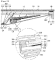


Classifications
-
- G—PHYSICS
- G02—OPTICS
- G02F—OPTICAL DEVICES OR ARRANGEMENTS FOR THE CONTROL OF LIGHT BY MODIFICATION OF THE OPTICAL PROPERTIES OF THE MEDIA OF THE ELEMENTS INVOLVED THEREIN; NON-LINEAR OPTICS; FREQUENCY-CHANGING OF LIGHT; OPTICAL LOGIC ELEMENTS; OPTICAL ANALOGUE/DIGITAL CONVERTERS
- G02F1/00—Devices or arrangements for the control of the intensity, colour, phase, polarisation or direction of light arriving from an independent light source, e.g. switching, gating or modulating; Non-linear optics
- G02F1/01—Devices or arrangements for the control of the intensity, colour, phase, polarisation or direction of light arriving from an independent light source, e.g. switching, gating or modulating; Non-linear optics for the control of the intensity, phase, polarisation or colour
- G02F1/13—Devices or arrangements for the control of the intensity, colour, phase, polarisation or direction of light arriving from an independent light source, e.g. switching, gating or modulating; Non-linear optics for the control of the intensity, phase, polarisation or colour based on liquid crystals, e.g. single liquid crystal display cells
- G02F1/133—Constructional arrangements; Operation of liquid crystal cells; Circuit arrangements
- G02F1/1333—Constructional arrangements; Manufacturing methods
- G02F1/1335—Structural association of cells with optical devices, e.g. polarisers or reflectors
- G02F1/1336—Illuminating devices
- G02F1/133602—Direct backlight
- G02F1/133603—Direct backlight with LEDs
-
- G—PHYSICS
- G02—OPTICS
- G02F—OPTICAL DEVICES OR ARRANGEMENTS FOR THE CONTROL OF LIGHT BY MODIFICATION OF THE OPTICAL PROPERTIES OF THE MEDIA OF THE ELEMENTS INVOLVED THEREIN; NON-LINEAR OPTICS; FREQUENCY-CHANGING OF LIGHT; OPTICAL LOGIC ELEMENTS; OPTICAL ANALOGUE/DIGITAL CONVERTERS
- G02F1/00—Devices or arrangements for the control of the intensity, colour, phase, polarisation or direction of light arriving from an independent light source, e.g. switching, gating or modulating; Non-linear optics
- G02F1/01—Devices or arrangements for the control of the intensity, colour, phase, polarisation or direction of light arriving from an independent light source, e.g. switching, gating or modulating; Non-linear optics for the control of the intensity, phase, polarisation or colour
- G02F1/13—Devices or arrangements for the control of the intensity, colour, phase, polarisation or direction of light arriving from an independent light source, e.g. switching, gating or modulating; Non-linear optics for the control of the intensity, phase, polarisation or colour based on liquid crystals, e.g. single liquid crystal display cells
- G02F1/133—Constructional arrangements; Operation of liquid crystal cells; Circuit arrangements
- G02F1/1333—Constructional arrangements; Manufacturing methods
- G02F1/1335—Structural association of cells with optical devices, e.g. polarisers or reflectors
- G02F1/1336—Illuminating devices
- G02F1/133602—Direct backlight
-
- G—PHYSICS
- G02—OPTICS
- G02B—OPTICAL ELEMENTS, SYSTEMS OR APPARATUS
- G02B6/00—Light guides; Structural details of arrangements comprising light guides and other optical elements, e.g. couplings
- G02B6/0001—Light guides; Structural details of arrangements comprising light guides and other optical elements, e.g. couplings specially adapted for lighting devices or systems
- G02B6/0011—Light guides; Structural details of arrangements comprising light guides and other optical elements, e.g. couplings specially adapted for lighting devices or systems the light guides being planar or of plate-like form
- G02B6/0033—Means for improving the coupling-out of light from the light guide
- G02B6/0035—Means for improving the coupling-out of light from the light guide provided on the surface of the light guide or in the bulk of it
- G02B6/0045—Means for improving the coupling-out of light from the light guide provided on the surface of the light guide or in the bulk of it by shaping at least a portion of the light guide
- G02B6/0046—Tapered light guide, e.g. wedge-shaped light guide
-
- G—PHYSICS
- G02—OPTICS
- G02B—OPTICAL ELEMENTS, SYSTEMS OR APPARATUS
- G02B6/00—Light guides; Structural details of arrangements comprising light guides and other optical elements, e.g. couplings
- G02B6/0001—Light guides; Structural details of arrangements comprising light guides and other optical elements, e.g. couplings specially adapted for lighting devices or systems
- G02B6/0011—Light guides; Structural details of arrangements comprising light guides and other optical elements, e.g. couplings specially adapted for lighting devices or systems the light guides being planar or of plate-like form
- G02B6/0033—Means for improving the coupling-out of light from the light guide
- G02B6/005—Means for improving the coupling-out of light from the light guide provided by one optical element, or plurality thereof, placed on the light output side of the light guide
- G02B6/0055—Reflecting element, sheet or layer
-
- G—PHYSICS
- G02—OPTICS
- G02F—OPTICAL DEVICES OR ARRANGEMENTS FOR THE CONTROL OF LIGHT BY MODIFICATION OF THE OPTICAL PROPERTIES OF THE MEDIA OF THE ELEMENTS INVOLVED THEREIN; NON-LINEAR OPTICS; FREQUENCY-CHANGING OF LIGHT; OPTICAL LOGIC ELEMENTS; OPTICAL ANALOGUE/DIGITAL CONVERTERS
- G02F1/00—Devices or arrangements for the control of the intensity, colour, phase, polarisation or direction of light arriving from an independent light source, e.g. switching, gating or modulating; Non-linear optics
- G02F1/01—Devices or arrangements for the control of the intensity, colour, phase, polarisation or direction of light arriving from an independent light source, e.g. switching, gating or modulating; Non-linear optics for the control of the intensity, phase, polarisation or colour
- G02F1/13—Devices or arrangements for the control of the intensity, colour, phase, polarisation or direction of light arriving from an independent light source, e.g. switching, gating or modulating; Non-linear optics for the control of the intensity, phase, polarisation or colour based on liquid crystals, e.g. single liquid crystal display cells
- G02F1/133—Constructional arrangements; Operation of liquid crystal cells; Circuit arrangements
- G02F1/1333—Constructional arrangements; Manufacturing methods
- G02F1/1335—Structural association of cells with optical devices, e.g. polarisers or reflectors
-
- G—PHYSICS
- G02—OPTICS
- G02F—OPTICAL DEVICES OR ARRANGEMENTS FOR THE CONTROL OF LIGHT BY MODIFICATION OF THE OPTICAL PROPERTIES OF THE MEDIA OF THE ELEMENTS INVOLVED THEREIN; NON-LINEAR OPTICS; FREQUENCY-CHANGING OF LIGHT; OPTICAL LOGIC ELEMENTS; OPTICAL ANALOGUE/DIGITAL CONVERTERS
- G02F1/00—Devices or arrangements for the control of the intensity, colour, phase, polarisation or direction of light arriving from an independent light source, e.g. switching, gating or modulating; Non-linear optics
- G02F1/01—Devices or arrangements for the control of the intensity, colour, phase, polarisation or direction of light arriving from an independent light source, e.g. switching, gating or modulating; Non-linear optics for the control of the intensity, phase, polarisation or colour
- G02F1/13—Devices or arrangements for the control of the intensity, colour, phase, polarisation or direction of light arriving from an independent light source, e.g. switching, gating or modulating; Non-linear optics for the control of the intensity, phase, polarisation or colour based on liquid crystals, e.g. single liquid crystal display cells
- G02F1/133—Constructional arrangements; Operation of liquid crystal cells; Circuit arrangements
- G02F1/1333—Constructional arrangements; Manufacturing methods
- G02F1/1335—Structural association of cells with optical devices, e.g. polarisers or reflectors
- G02F1/133524—Light-guides, e.g. fibre-optic bundles, louvered or jalousie light-guides
-
- G—PHYSICS
- G02—OPTICS
- G02F—OPTICAL DEVICES OR ARRANGEMENTS FOR THE CONTROL OF LIGHT BY MODIFICATION OF THE OPTICAL PROPERTIES OF THE MEDIA OF THE ELEMENTS INVOLVED THEREIN; NON-LINEAR OPTICS; FREQUENCY-CHANGING OF LIGHT; OPTICAL LOGIC ELEMENTS; OPTICAL ANALOGUE/DIGITAL CONVERTERS
- G02F1/00—Devices or arrangements for the control of the intensity, colour, phase, polarisation or direction of light arriving from an independent light source, e.g. switching, gating or modulating; Non-linear optics
- G02F1/01—Devices or arrangements for the control of the intensity, colour, phase, polarisation or direction of light arriving from an independent light source, e.g. switching, gating or modulating; Non-linear optics for the control of the intensity, phase, polarisation or colour
- G02F1/13—Devices or arrangements for the control of the intensity, colour, phase, polarisation or direction of light arriving from an independent light source, e.g. switching, gating or modulating; Non-linear optics for the control of the intensity, phase, polarisation or colour based on liquid crystals, e.g. single liquid crystal display cells
- G02F1/133—Constructional arrangements; Operation of liquid crystal cells; Circuit arrangements
- G02F1/1333—Constructional arrangements; Manufacturing methods
- G02F1/1335—Structural association of cells with optical devices, e.g. polarisers or reflectors
- G02F1/133553—Reflecting elements
-
- G—PHYSICS
- G02—OPTICS
- G02F—OPTICAL DEVICES OR ARRANGEMENTS FOR THE CONTROL OF LIGHT BY MODIFICATION OF THE OPTICAL PROPERTIES OF THE MEDIA OF THE ELEMENTS INVOLVED THEREIN; NON-LINEAR OPTICS; FREQUENCY-CHANGING OF LIGHT; OPTICAL LOGIC ELEMENTS; OPTICAL ANALOGUE/DIGITAL CONVERTERS
- G02F1/00—Devices or arrangements for the control of the intensity, colour, phase, polarisation or direction of light arriving from an independent light source, e.g. switching, gating or modulating; Non-linear optics
- G02F1/01—Devices or arrangements for the control of the intensity, colour, phase, polarisation or direction of light arriving from an independent light source, e.g. switching, gating or modulating; Non-linear optics for the control of the intensity, phase, polarisation or colour
- G02F1/13—Devices or arrangements for the control of the intensity, colour, phase, polarisation or direction of light arriving from an independent light source, e.g. switching, gating or modulating; Non-linear optics for the control of the intensity, phase, polarisation or colour based on liquid crystals, e.g. single liquid crystal display cells
- G02F1/133—Constructional arrangements; Operation of liquid crystal cells; Circuit arrangements
- G02F1/1333—Constructional arrangements; Manufacturing methods
- G02F1/1335—Structural association of cells with optical devices, e.g. polarisers or reflectors
- G02F1/1336—Illuminating devices
- G02F1/133602—Direct backlight
- G02F1/133605—Direct backlight including specially adapted reflectors
-
- G—PHYSICS
- G02—OPTICS
- G02F—OPTICAL DEVICES OR ARRANGEMENTS FOR THE CONTROL OF LIGHT BY MODIFICATION OF THE OPTICAL PROPERTIES OF THE MEDIA OF THE ELEMENTS INVOLVED THEREIN; NON-LINEAR OPTICS; FREQUENCY-CHANGING OF LIGHT; OPTICAL LOGIC ELEMENTS; OPTICAL ANALOGUE/DIGITAL CONVERTERS
- G02F1/00—Devices or arrangements for the control of the intensity, colour, phase, polarisation or direction of light arriving from an independent light source, e.g. switching, gating or modulating; Non-linear optics
- G02F1/01—Devices or arrangements for the control of the intensity, colour, phase, polarisation or direction of light arriving from an independent light source, e.g. switching, gating or modulating; Non-linear optics for the control of the intensity, phase, polarisation or colour
- G02F1/13—Devices or arrangements for the control of the intensity, colour, phase, polarisation or direction of light arriving from an independent light source, e.g. switching, gating or modulating; Non-linear optics for the control of the intensity, phase, polarisation or colour based on liquid crystals, e.g. single liquid crystal display cells
- G02F1/133—Constructional arrangements; Operation of liquid crystal cells; Circuit arrangements
- G02F1/1333—Constructional arrangements; Manufacturing methods
- G02F1/1335—Structural association of cells with optical devices, e.g. polarisers or reflectors
- G02F1/1336—Illuminating devices
- G02F1/133615—Edge-illuminating devices, i.e. illuminating from the side
-
- G—PHYSICS
- G02—OPTICS
- G02B—OPTICAL ELEMENTS, SYSTEMS OR APPARATUS
- G02B6/00—Light guides; Structural details of arrangements comprising light guides and other optical elements, e.g. couplings
- G02B6/0001—Light guides; Structural details of arrangements comprising light guides and other optical elements, e.g. couplings specially adapted for lighting devices or systems
- G02B6/0011—Light guides; Structural details of arrangements comprising light guides and other optical elements, e.g. couplings specially adapted for lighting devices or systems the light guides being planar or of plate-like form
- G02B6/0075—Arrangements of multiple light guides
- G02B6/0078—Side-by-side arrangements, e.g. for large area displays
-
- G—PHYSICS
- G02—OPTICS
- G02B—OPTICAL ELEMENTS, SYSTEMS OR APPARATUS
- G02B6/00—Light guides; Structural details of arrangements comprising light guides and other optical elements, e.g. couplings
- G02B6/0001—Light guides; Structural details of arrangements comprising light guides and other optical elements, e.g. couplings specially adapted for lighting devices or systems
- G02B6/0011—Light guides; Structural details of arrangements comprising light guides and other optical elements, e.g. couplings specially adapted for lighting devices or systems the light guides being planar or of plate-like form
- G02B6/0081—Mechanical or electrical aspects of the light guide and light source in the lighting device peculiar to the adaptation to planar light guides, e.g. concerning packaging
- G02B6/0086—Positioning aspects
- G02B6/0088—Positioning aspects of the light guide or other optical sheets in the package
-
- G—PHYSICS
- G02—OPTICS
- G02F—OPTICAL DEVICES OR ARRANGEMENTS FOR THE CONTROL OF LIGHT BY MODIFICATION OF THE OPTICAL PROPERTIES OF THE MEDIA OF THE ELEMENTS INVOLVED THEREIN; NON-LINEAR OPTICS; FREQUENCY-CHANGING OF LIGHT; OPTICAL LOGIC ELEMENTS; OPTICAL ANALOGUE/DIGITAL CONVERTERS
- G02F1/00—Devices or arrangements for the control of the intensity, colour, phase, polarisation or direction of light arriving from an independent light source, e.g. switching, gating or modulating; Non-linear optics
- G02F1/01—Devices or arrangements for the control of the intensity, colour, phase, polarisation or direction of light arriving from an independent light source, e.g. switching, gating or modulating; Non-linear optics for the control of the intensity, phase, polarisation or colour
- G02F1/13—Devices or arrangements for the control of the intensity, colour, phase, polarisation or direction of light arriving from an independent light source, e.g. switching, gating or modulating; Non-linear optics for the control of the intensity, phase, polarisation or colour based on liquid crystals, e.g. single liquid crystal display cells
- G02F1/133—Constructional arrangements; Operation of liquid crystal cells; Circuit arrangements
- G02F1/1333—Constructional arrangements; Manufacturing methods
- G02F1/1335—Structural association of cells with optical devices, e.g. polarisers or reflectors
- G02F1/1336—Illuminating devices
- G02F1/133602—Direct backlight
- G02F1/133611—Direct backlight including means for improving the brightness uniformity
Definitions
- the present disclosure relates to a display device.
- LCD liquid crystal display device
- PDP plasma display panel
- ELD electro luminescent display
- VFD vacuum fluorescent display
- the liquid crystal panel of the LCD includes a liquid crystal layer, and a TFT substrate and a color filter substrate that face each other with the liquid crystal layer interposed therebetween, and may display an image using light provided by a backlight unit.
- the disclosure has been intended to solve the aforementioned problems and other problems.
- the disclosure is to improve the contrast ratio of a display device and also reduce consumption power of the display device.
- the disclosure is to improve a light characteristic or light distribution of a display device.
- the disclosure is to implement the slim structure of a display device.
- a display panel a frame positioned at the back of the display panel, a main light assembly positioned on the frame between the display panel and the frame, and a side light assembly positioned on the frame between the display panel and the frame and positioned to be adjacent to the main light assembly.
- the frame includes a bottom forming a lower surface and a side support extended from the bottom to one side of the display panel, the side support is closer to the display panel than the bottom, the main light assembly is positioned at the bottom, and he side light assembly is positioned at the side support.
- the main light assembly may include a substrate positioned on the bottom, a plurality of light sources sequentially mounted on the substrate, and a plurality of lenses mounted on the substrate and corresponding to the plurality of light sources, respectively.
- the side light assembly may include a light guide panel positioned between the display panel and the side support, a light source positioned adjacent to one side surface of the light guide panel, and a reflection plate positioned at the bottom of the light guide panel.
- the light guide panel may include a light incidence portion positioned to neighbor the light source, a light output portion forming the top of the light guide panel, and a slope portion forming the bottom of the light guide panel and having a distance closer to the light output portion as the slope portion becomes distant from the light source.
- the reflection plate may be bonded to the slope portion.
- the display device may further include a substrate on which the light source is mounted, a lower cover positioned on the lower side of the substrate, and an upper cover positioned on an upper side of the light source and coupled to the lower cover.
- the lower cover may include a base supporting the substrate and an extension portion extended from the base to the light guide panel and supporting the light guide panel.
- the upper cover may include a light hole formed at the top of the light source, and the light source may provide light toward at least the upper cover.
- the display device may further include a reflection sheet positioned between the main light assembly and the display panel.
- the reflection sheet may include a first part positioned on the bottom or the substrate, a second part extended from the first part to the side light assembly, and a third part elongated from the second part and covering a part of the side light assembly.
- the frame may further include a stepped portion formed between the bottom and the side support.
- the side support may include a first side support positioned on one side of the bottom and a second side support positioned on the other side of the bottom.
- the side light assembly may include a first side light assembly positioned on the first side support and a second side light assembly positioned on the second side support.
- the contrast ratio of the display device can be improved, and consumption power of the display device can also be improved.
- a light characteristic or light distribution of the display device can be improved.
- the slim structure of the display device can be implemented.
- a display panel is described by taking a liquid crystal display device (LCD) as an example, but the display panel capable of being applied to the disclosure is not limited to the LCD and may be applied to a plasma display panel (PDP), a field emission display (FED), and an organic light emitting diode (OLED).
- LCD liquid crystal display device
- PDP plasma display panel
- FED field emission display
- OLED organic light emitting diode
- FIGS. 1 and 2 are diagrams illustrating an example of a display device related to the disclosure.
- the display device 100 may include a first long side LS1, a second long side LS2 opposite the first long side LS1, a first short side SS1 neighboring the first long side LS1 and the second long side LS2, and a second short side SS2 opposite the first short side SS1.
- the area of the first short side SS1 may be called a first side area.
- the area of the second short side SS2 may be called a second side area opposite the first side area.
- the area of the first long side LS1 may be called a third side area neighboring the first side area and the second side area and positioned between the first side area and the second side area.
- the area of the second long side LS2 may be called a fourth side area neighboring the first side area and the second side area, positioned between the first side area and the second side area, and opposite the third side area.
- the length of the first or second long side LS1, LS2 has been illustrated as being longer than the length of the first, second short side SS1, SS2, but the length of the first, second long side LS1, LS2 may be approximately the same as that of the first, second short side SS1, SS2.
- a first direction DR1 may be a direction parallel to the long side LS1, LS2 of the display device 100.
- a second direction DR2 may be a direction parallel to the short side SS1, SS2 of the display device 100.
- a third direction DR3 may be a direction perpendicular to the first direction DR1 and/or the second direction DR2.
- the first direction DR1 and the second direction DR2 may be collectively called a horizontal direction. Furthermore, the third direction DR3 may be called a vertical direction.
- the side on which the display device 100 displays an image may be called a front or front surface.
- the side on which the image cannot be viewed may be called a rear or rear surface.
- the side of the first long side LS1 may be called a top or top surface.
- the side of the second long side LS2 may be called a bottom or bottom surface.
- the side of the second short side SS2 may be called the left side or a left surface
- the first short side SS1 may be called the right side or a right surface.
- first long side LS1, the second long side LS2, the first short side SS1, and the second short side SS2 may be called the edges of the display device 100. Furthermore, points where the first long side LS1, the second long side LS2, the first short side SS1, and the second short side SS2 meet may be called corners.
- the point where the first long side LS1 and the first short side SS1 meet may be called a first corner C 1
- the point where the first long side LS1 and the second short side SS2 meet may be called a second corner C 2
- the point where the second short side SS2 and the second long side LS2 meet may be called a third corner C 3
- the point where the second long side LS2 and the first short side SS1 meet may be called a fourth corner C 4 .
- a direction from the first short side SS1 to the second short side SS1 or a direction from the second short side SS2 to the first short side SS1 may be called a left and right LR.
- a direction from the first long side LS1 to the second long side LS2 or a direction from the second long side LS2 to the first long side LS1 may be called an up and down UD.
- a front cover 105 may cover at least some of the front and side of the display panel 110.
- the front cover 105 may have a quadrangular frame shape having an empty center.
- the front cover 105 may include a front surface cover and a side cover. That is, the front cover may be divided into the front surface cover positioned on the front side of the display panel 110 and the side cover positioned on the side of the display panel 110.
- the front surface cover and the side cover may be separately configured. Any one of the front surface cover and the side cover may be omitted.
- a display panel 110 is provided at the front of the display device 100, and an image may be displayed on the display panel.
- the display panel 110 may divide an image into a plurality of pixels and output the image in accordance with a color, brightness, and chroma per pixel.
- the display panel 110 may be divided into an active area in which an image is displayed and an inactive area in which an image is not displayed.
- the display panel 110 may include a front substrate and a rear substrate opposite each other with a liquid crystal layer interposed therebetween.
- the front substrate may include a plurality of pixels configured with red (R), green (G) and blue (B) subpixels.
- the rear substrate may include switching elements.
- the rear substrate may switch a pixel electrode.
- the pixel electrode may change the array of the molecules of the liquid crystal layer in response to an external control signal.
- the liquid crystal layer may include a plurality of liquid crystal molecules.
- the array of the liquid crystal molecules may be changed in accordance with a voltage difference generated between the pixel electrode and a common electrode.
- the liquid crystal layer may block or transmit, toward the front substrate, light provided by a backlight unit 120.
- the backlight unit 120 may be positioned at the back of the display panel 110.
- the backlight unit 120 may include a plurality of light sources.
- the light sources of the backlight unit 120 may have a direct type or an edge type.
- the edge type backlight unit 120 may further include a light guide panel.
- the backlight unit 120 may be driven using a full driving method or a partial driving method, such as local dimming or impulsive.
- the backlight unit 120 may include an optical sheet 125 and an optical layer 123.
- the optical sheet 125 may uniformly transmit, to the display panel 110, light provided by a light source.
- the optical sheet 125 may be configured with a plurality of layers.
- the optical sheet 125 may include at least one prism sheet and/or at least one diffusion sheet.
- the optical sheet 125 may include at least one coupling part 125d.
- the coupling part 125d may be coupled to the front cover 105 and/or a back cover 150.
- the coupling part 125d may be coupled to a structure mounted on the front cover 105 and/or the back cover 150.
- the optical layer 123 may include the light source, etc. A detailed element of the optical layer 123 is described in a corresponding part.
- a frame 130 may function to support the elements of the display device 100.
- an element such as the backlight unit 120, may be coupled to the frame 130.
- the frame 130 may be made of a metal material, such as an aluminum alloy, and may provide stiffness to the display device 100.
- the back cover 150 may be positioned at the back of the frame 130.
- the back cover 150 can protect internal elements against the outside. At least some of the back cover 150 may be coupled to the frame 130 and/or the front cover 105.
- the back cover 150 may be an injected matter of a resin material.
- the frame 130 may include a bottom 130B and side supports 130S1 and 130S2.
- the bottom 130B may be a flat plate.
- the side supports 130S1 and 130S2 may be positioned on one side or both sides of the bottom 130B, and may be positioned over the bottom 130B.
- the bottom 130B and the side supports 130S1 and 130S2 may form a step.
- the frame 130 may have stepped portions 130I 1 and 130I 2 .
- the stepped portions 130I 1 and 130I 2 may be extended from the bottom 130B to the side supports 130S1 and 130S2.
- each of the stepped portions 130I 1 and 13012 may have a slope.
- a distance D1 from the display panel 110 to the bottom 130B may be greater than a distance DS1 or DS2 from the display panel 110 to the side support 130S1 or 130S2.
- the distance DS1 from the display panel 110 to the first side support 130S1 may be the same as the distance DS2 from the display panel 110 to the second side support 130S2.
- the distances D1, DS2, and DS3 may be called optical distances.
- a main light assembly LA may be positioned on the bottom 130B.
- a first light assembly LA1 may be positioned on the first side support 130S1.
- a second light assembly LA2 may be positioned on the second side support 130S2.
- the first light assembly LA1 and/or the second light assembly LA2 may be different from the main light assembly LA.
- the first light assembly LA1 may be the same as the second light assembly LA2.
- the main light assembly LA may include a substrate 122 and a plurality of lenses 124.
- the substrate 122 may be lengthily elongated to the left and right of the bottom 130B.
- a plurality of light sources LS may be sequentially mounted on the substrate 122.
- the plurality of lenses 124 may be mounted on the substrate 122 in accordance with the plurality of light sources LS, respectively.
- a plurality of the substrates 122 may be sequentially arranged in the up and down direction of the bottom 130B.
- a housing 1223 may be mounted on a substrate 1220.
- a light source 1224 may be received in or mounted on the housing 1223.
- the light source 1224 may provide light from the housing 1223 to the lateral direction of the housing 1223.
- a reflection sheet 1221 may be positioned on the substrate 1220.
- a reflection pattern 1222 may be formed on the reflection sheet 1221.
- a resin layer 1226 may be formed over the substrate 1220 in such a way as to cover the reflection sheet 1221 and/or the reflection pattern 1222 and/or the housing 1223.
- the resin layer 1226 may be a transparent substance.
- the resin layer 1226 may fully cover the housing 1223.
- the reflection pattern 1222 may be formed on the top or top surface of the resin layer 1226. Accordingly, light LP provided from the light source 1224 to the side of the housing 1223 may be reflected and/or scattered and uniformly spread to the entire resin layer 1226.
- the aforementioned contents may be an example of a first light assembly or a second light assembly.
- a light source 1224 may be mounted on a housing 1223.
- the housing 1223 may be mounted on the substrate 122.
- a reflection sheet 1221 may be positioned on the substrate 122.
- the reflection sheet 1221 may partially overlap the substrate 122 in order to be adjacent to the light source 1224 or the housing 1223.
- An optical sheet 1228 may be positioned over the reflection sheet 1221 and/or the light source 1224 and/or the substrate 122, and may be spaced apart therefrom. That is, an empty space AG may be formed between the optical sheet 1228 and the reflection sheet 1221.
- the optical sheet 1228 may be spaced apart from the reflection sheet 1221 by a support 1227.
- the optical sheet 1228 may include a plurality of holes h.
- the plurality of holes h may be formed to penetrate the optical sheet 1228.
- the size of a second hole h12 may be greater than the size of a first hole h11.
- the size of a third hole h13 may be greater than the size of the second hole h12. That is, the sizes of the plurality of holes h may be greater as the plurality of holes becomes distant in a horizontal direction from the light source 1224. Accordingly, a light distribution may be uniform regardless of the light source 1224.
- the optical sheet 1228 may include a reflection surface RF.
- the reflection surface RF may be formed on the bottom of the optical sheet 1228. Accordingly, light may be reflected and/or scattered between the reflection sheet 1221 and the optical sheet 1228. The reflected and/or scattered light may be externally output through the plurality of holes h.
- the aforementioned contents may be an example of the first light assembly LA1 or a second light assembly LA2.
- a light source 220 may be mounted on a substrate 210.
- the substrate 210 may be a PCB.
- the light source 220 may be electrically connected to the substrate 210.
- the light source 220 may provide light in the lateral direction of the substrate 210. This may be called a side view type.
- a light guide panel 230 may be positioned over the substrate 210.
- the light source 220 may be positioned on one side of the light guide panel 230.
- the light guide panel 230 may include an introduction part 231, a slope portion 232, and a light output portion 233.
- the introduction part 231 may form one side of the light guide panel 230.
- the introduction part 231 may neighbor the light source 220 or come into contact with the light source 220.
- the slope portion 232 may form the lower surface of the light guide panel 230.
- the slope portion 232 may have a positive slope with respect to the center of the light source 220. This may mean that the slope portion 232 may have an ascent slope as it becomes distant from the light source 220.
- the light output portion 233 may form the upper surface of the light guide panel 230.
- the light output portion 233 may face the slope portion 232.
- a stepped portion 234 may be formed between the introduction part 231 and the light output portion 233.
- the introduction part 231 may be called a light incidence portion 231.
- a lower cover 240 may be positioned on the lower side of the substrate 210 and/or under the light guide panel 230.
- the lower cover 240 may receive the substrate 210 and the light source 220 and support the light guide panel 230.
- the lower cover 240 may include a base 242.
- the base 242 may be a lengthily elongated flat panel.
- the lower cover 240 may include an extension portion 244.
- the extension portion 244 may be extended from the light source 220 to a direction toward the light guide panel 230.
- the base 242 and the extension portion 244 may form a step 246.
- An upper cover 250 may be coupled to the lower cover 240.
- the upper cover 250 may press the light guide panel 230 from the upper side.
- the upper cover 250 may cover the top of the light source 220.
- the upper cover 250 and the lower cover 240 may be metal.
- a reflection plate 235 may be positioned at the bottom of the light guide panel 230 or may come into contact with the bottom of the light guide panel 230 or may be formed on the bottom of the light guide panel 230.
- the reflection plate 235 may be a reflection sheet or may be a coated reflection material.
- the aforementioned contents may be an example of the first light assembly LA1 or the second light assembly LA2.
- the light guide panel 230 may be a plural number.
- the plurality of light guide panels 230 may be sequentially arranged.
- a first light guide panel U1 may be positioned on one side
- a second light guide panel U2 may neighbor the first light guide panel U1
- a third light guide panel U3 may neighbor the second light guide panel U2
- a fourth light guide panel U4 may neighbor the third light guide panel U3
- a fifth light guide panel U5 may neighbor the fourth light guide panel U4
- a sixth light guide panel U6 may neighbor the fifth light guide panel U5.
- a single or a plurality of the light sources 220 (refer to FIG. 7 ) may be arranged in accordance with the light guide panels U1-U6. Accordingly, the amount of light can be locally adjusted.
- the aforementioned contents may be an example of the first light assembly LA1 or the second light assembly LA2.
- the first light assembly LA1 and/or the second light assembly LA2 may be called a side light assembly.
- the main light assembly LA may be positioned on the bottom 130B of the frame 130.
- the side light assemblies LA1 and LA2 may include an eleventh light assembly LA11, a twelfth light assembly LA12, a twenty-first light assembly LA21, and a twenty-second light assembly LA22.
- the eleventh light assembly LA11 and/or the twelfth light assembly LA12 may be positioned on the first side support 130S1.
- the twenty-first light assembly LA21 and/or the twenty-second light assembly LA22 may be positioned on the second side support 130S2.
- a connector CN may be electrically connected to a plurality of the substrates 122. Externally supplied power may be provided to the light sources LS provided in the main light assembly LA through the plurality of substrates 122.
- the frame 130 may include a flange 130P.
- the flange 130P may be formed at one end of the side support 130S1.
- the flange 130P may support a side frame SF.
- the optical sheet 125 may be supported by the flange 130P, and may be positioned under the display panel 110.
- the side frame SF may include a horizontal portion SF1 and a vertical portion SF2.
- the vertical portion SF2 may form an external appearance of the display device.
- An adhesion member AD may be fixed on the horizontal portion SF1, and the display panel 110 may be fixed to the adhesion member AD.
- the adhesion member AD may be a double-sided tape.
- a reflection sheet 300 may include a first part 310, a second part 320, and a third part 330.
- the first part 310 may be positioned on the bottom 130B of the frame 130.
- the first part 310 may include a hole (not illustrated) through which the lens 124 passes.
- the second part 320 may be extended from the first part 310 to the side light assembly LA1.
- the second part 320 may face the stepped portion 130I1.
- the third part 330 may be positioned on the side light assembly LA1.
- the third part 330 may be fixed on the upper cover 250 of the side light assembly LA1.
- One end of the third part 330 may be adjacent to the side of the stepped portion 234 of the light guide panel 230 or may come into contact with the side of the stepped portion 234 of the light guide panel 230.
- the third part 330 may be coupled to the second part 320. Accordingly, a dark area which may be formed between the main light assembly LA and the side light assembly LA1 can be improved, and a light distribution provided to the display panel 110 can be uniform.
- the side support 130S1 may be extended from the bottom 130B to the flange 130P.
- the side support 130S1 may have a gentle slope from the bottom 130B to the flange 130P.
- the side light assembly LA1 may be positioned over the side support 130S1. Accordingly, a dark area which may be formed between the main light assembly LA and the side light assembly LA1 can be improved, and a light distribution provided to the display panel 110 can become more uniform.
- the light source 220 may have many-sided light.
- the light source 220 may be an LED capable of 5-sided light emission.
- the light source 220 may be an LED capable of 4-sided light emission.
- a wall LW may cover one side of the light source 220.
- the upper cover 250 may be a plate lengthily elongated in the length direction of one side of the light guide panel 230.
- the upper cover 250 may be coupled to the lower cover 240 (refer to FIG. 7 ) by a fastening member f.
- the upper cover 250 may include a light hole LH.
- a plurality of the light holes LH may be formed in the upper cover 250.
- the light hole LH may be positioned at the top of the light source 220 (refer to FIG. 7 ).
- the number of light holes LH may correspond to the number of light sources 220 (refer to FIG. 7 ).
- light emitted from the light source 220 to the light guide panel 230 may pass through the introduction part 231, may be reflected within the light guide panel 230, and may be spread to the entire light guide panel 230. Accordingly, the light guide panel 230 can uniformly provide light to the display panel 110.
- Light provided from the light source 220 to the upper side of the light source 220 may be provided to the display panel 110 through the light hole LH of the upper cover 250. Accordingly, light having a distribution identical with or similar to that of the main light assembly LA and the side light assembly LA1 can be provided between the main light assembly LA and the side light assembly LA1.
Landscapes
- Physics & Mathematics (AREA)
- Nonlinear Science (AREA)
- General Physics & Mathematics (AREA)
- Optics & Photonics (AREA)
- Mathematical Physics (AREA)
- Chemical & Material Sciences (AREA)
- Crystallography & Structural Chemistry (AREA)
- Liquid Crystal (AREA)
- Planar Illumination Modules (AREA)
Abstract
Description
- The present disclosure relates to a display device.
- With the development of the information society, the demand for a display device is increased in various forms. Accordingly, various display devices, such as a liquid crystal display device (LCD), a plasma display panel (PDP), an electro luminescent display (ELD), and a vacuum fluorescent display (VFD), are recently researched and used.
- From among them, the liquid crystal panel of the LCD includes a liquid crystal layer, and a TFT substrate and a color filter substrate that face each other with the liquid crystal layer interposed therebetween, and may display an image using light provided by a backlight unit.
- The disclosure has been intended to solve the aforementioned problems and other problems. The disclosure is to improve the contrast ratio of a display device and also reduce consumption power of the display device.
- The disclosure is to improve a light characteristic or light distribution of a display device.
- The disclosure is to implement the slim structure of a display device.
- According to an aspect of the disclosure, there is provided a display panel, a frame positioned at the back of the display panel, a main light assembly positioned on the frame between the display panel and the frame, and a side light assembly positioned on the frame between the display panel and the frame and positioned to be adjacent to the main light assembly. The frame includes a bottom forming a lower surface and a side support extended from the bottom to one side of the display panel, the side support is closer to the display panel than the bottom, the main light assembly is positioned at the bottom, and he side light assembly is positioned at the side support.
- Furthermore, according to another aspect of the disclosure, the main light assembly may include a substrate positioned on the bottom, a plurality of light sources sequentially mounted on the substrate, and a plurality of lenses mounted on the substrate and corresponding to the plurality of light sources, respectively.
- Furthermore, according to another aspect of the disclosure, the side light assembly may include a light guide panel positioned between the display panel and the side support, a light source positioned adjacent to one side surface of the light guide panel, and a reflection plate positioned at the bottom of the light guide panel.
- Furthermore, according to another aspect of the disclosure, the light guide panel may include a light incidence portion positioned to neighbor the light source, a light output portion forming the top of the light guide panel, and a slope portion forming the bottom of the light guide panel and having a distance closer to the light output portion as the slope portion becomes distant from the light source.
- Furthermore, according to another aspect of the disclosure, the reflection plate may be bonded to the slope portion.
- Furthermore, according to another aspect of the disclosure, the display device may further include a substrate on which the light source is mounted, a lower cover positioned on the lower side of the substrate, and an upper cover positioned on an upper side of the light source and coupled to the lower cover. The lower cover may include a base supporting the substrate and an extension portion extended from the base to the light guide panel and supporting the light guide panel.
- Furthermore, according to another aspect of the disclosure, the upper cover may include a light hole formed at the top of the light source, and the light source may provide light toward at least the upper cover.
- Furthermore, according to another aspect of the disclosure, the display device may further include a reflection sheet positioned between the main light assembly and the display panel. The reflection sheet may include a first part positioned on the bottom or the substrate, a second part extended from the first part to the side light assembly, and a third part elongated from the second part and covering a part of the side light assembly.
- Furthermore, according to another aspect of the disclosure, the frame may further include a stepped portion formed between the bottom and the side support.
- Furthermore, according to another aspect of the disclosure, the side support may include a first side support positioned on one side of the bottom and a second side support positioned on the other side of the bottom. The side light assembly may include a first side light assembly positioned on the first side support and a second side light assembly positioned on the second side support.
- Effects of the display device according to the disclosure are as follows.
- According to at least one of embodiments of the disclosure, the contrast ratio of the display device can be improved, and consumption power of the display device can also be improved.
- According to at least one of embodiments of the disclosure, a light characteristic or light distribution of the display device can be improved.
- According to at least one of embodiments of the disclosure, the slim structure of the display device can be implemented.
- An additional scope of the applicability of the disclosure will become evident from the following detailed description. However, various changes and modifications may be evidently understood by those skilled in the art within the spirit and scope of the disclosure. Accordingly, it is to be understood that the detailed description and a specific embodiment, such as a specific embodiment of the disclosure, are merely given as examples.
-
-
FIGS. 1 and2 are diagrams illustrating an example of a display device related to the disclosure. -
FIG. 3 is a diagram illustrating an example of a frame according to an embodiment of the disclosure. -
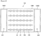
FIG. 4 is a diagram illustrating an example of the deployment of a light assembly according to an embodiment of the disclosure. -
FIGS. 5 to 9 are diagrams illustrating examples of light assemblies according to an embodiment of the disclosure. -
FIGS. 10 to 12 are diagrams illustrating examples of a light assembly structure according to an embodiment of the disclosure. -
FIGS. 13 to 17 are diagrams illustrating other examples of a light assembly according to an embodiment of the disclosure. - Hereinafter, embodiments disclosed in the disclosure are described in detail with reference to the accompanying drawings. The same or similar element is assigned the same reference numeral regardless of its reference numeral, and a redundant description thereof is omitted.
- It is to be noted that the suffixes of elements used in the following description, such as a "module" and a "unit", are assigned or interchangeable with each other by taking into consideration only the ease of writing this specification, but in themselves are not particularly given distinct meanings and roles. Furthermore, in describing the embodiments disclosed in this specification, a detailed description of a related known technology will be omitted if it is deemed to make the gist of the disclosure unnecessarily vague. Furthermore, the accompanying drawings are merely intended to make easily understood the exemplary embodiments disclosed in this specification, and the technical spirit disclosed in this specification is not restricted by the accompanying drawings and includes all modifications, equivalents, and substitutions which fall within the spirit and technological scope of the disclosure.
- Hereinafter, a display panel is described by taking a liquid crystal display device (LCD) as an example, but the display panel capable of being applied to the disclosure is not limited to the LCD and may be applied to a plasma display panel (PDP), a field emission display (FED), and an organic light emitting diode (OLED).
-
FIGS. 1 and2 are diagrams illustrating an example of a display device related to the disclosure. - Hereinafter, the
display device 100 may include a first long side LS1, a second long side LS2 opposite the first long side LS1, a first short side SS1 neighboring the first long side LS1 and the second long side LS2, and a second short side SS2 opposite the first short side SS1. - In this case, the area of the first short side SS1 may be called a first side area. The area of the second short side SS2 may be called a second side area opposite the first side area. The area of the first long side LS1 may be called a third side area neighboring the first side area and the second side area and positioned between the first side area and the second side area. The area of the second long side LS2 may be called a fourth side area neighboring the first side area and the second side area, positioned between the first side area and the second side area, and opposite the third side area.
- Furthermore, for convenience of description, the length of the first or second long side LS1, LS2 has been illustrated as being longer than the length of the first, second short side SS1, SS2, but the length of the first, second long side LS1, LS2 may be approximately the same as that of the first, second short side SS1, SS2.
- Furthermore, hereinafter, a first direction DR1 may be a direction parallel to the long side LS1, LS2 of the
display device 100. A second direction DR2 may be a direction parallel to the short side SS1, SS2 of thedisplay device 100. A third direction DR3 may be a direction perpendicular to the first direction DR1 and/or the second direction DR2. - The first direction DR1 and the second direction DR2 may be collectively called a horizontal direction. Furthermore, the third direction DR3 may be called a vertical direction.
- From a different viewpoint, the side on which the
display device 100 displays an image may be called a front or front surface. When thedisplay device 100 displays an image, the side on which the image cannot be viewed may be called a rear or rear surface. When thedisplay device 100 is viewed from the front or front surface, the side of the first long side LS1 may be called a top or top surface. Likewise, the side of the second long side LS2 may be called a bottom or bottom surface. Likewise, the side of the second short side SS2 may be called the left side or a left surface, and the first short side SS1 may be called the right side or a right surface. - Furthermore, the first long side LS1, the second long side LS2, the first short side SS1, and the second short side SS2 may be called the edges of the
display device 100. Furthermore, points where the first long side LS1, the second long side LS2, the first short side SS1, and the second short side SS2 meet may be called corners. For example, the point where the first long side LS1 and the first short side SS1 meet may be called a first corner C1, the point where the first long side LS1 and the second short side SS2 meet may be called a second corner C2, the point where the second short side SS2 and the second long side LS2 meet may be called a third corner C3, and the point where the second long side LS2 and the first short side SS1 meet may be called a fourth corner C4. - In this case, a direction from the first short side SS1 to the second short side SS1 or a direction from the second short side SS2 to the first short side SS1 may be called a left and right LR. A direction from the first long side LS1 to the second long side LS2 or a direction from the second long side LS2 to the first long side LS1 may be called an up and down UD.
- A
front cover 105 may cover at least some of the front and side of thedisplay panel 110. Thefront cover 105 may have a quadrangular frame shape having an empty center. - The
front cover 105 may include a front surface cover and a side cover. That is, the front cover may be divided into the front surface cover positioned on the front side of thedisplay panel 110 and the side cover positioned on the side of thedisplay panel 110. The front surface cover and the side cover may be separately configured. Any one of the front surface cover and the side cover may be omitted. - A
display panel 110 is provided at the front of thedisplay device 100, and an image may be displayed on the display panel. Thedisplay panel 110 may divide an image into a plurality of pixels and output the image in accordance with a color, brightness, and chroma per pixel. Thedisplay panel 110 may be divided into an active area in which an image is displayed and an inactive area in which an image is not displayed. Thedisplay panel 110 may include a front substrate and a rear substrate opposite each other with a liquid crystal layer interposed therebetween. - The front substrate may include a plurality of pixels configured with red (R), green (G) and blue (B) subpixels. The rear substrate may include switching elements. The rear substrate may switch a pixel electrode. For example, the pixel electrode may change the array of the molecules of the liquid crystal layer in response to an external control signal. The liquid crystal layer may include a plurality of liquid crystal molecules. The array of the liquid crystal molecules may be changed in accordance with a voltage difference generated between the pixel electrode and a common electrode. The liquid crystal layer may block or transmit, toward the front substrate, light provided by a
backlight unit 120. - The
backlight unit 120 may be positioned at the back of thedisplay panel 110. Thebacklight unit 120 may include a plurality of light sources. The light sources of thebacklight unit 120 may have a direct type or an edge type. The edgetype backlight unit 120 may further include a light guide panel. - The
backlight unit 120 may be driven using a full driving method or a partial driving method, such as local dimming or impulsive. Thebacklight unit 120 may include anoptical sheet 125 and anoptical layer 123. - The
optical sheet 125 may uniformly transmit, to thedisplay panel 110, light provided by a light source. Theoptical sheet 125 may be configured with a plurality of layers. For example, theoptical sheet 125 may include at least one prism sheet and/or at least one diffusion sheet. - The
optical sheet 125 may include at least onecoupling part 125d. Thecoupling part 125d may be coupled to thefront cover 105 and/or aback cover 150. Alternatively, thecoupling part 125d may be coupled to a structure mounted on thefront cover 105 and/or theback cover 150. - The
optical layer 123 may include the light source, etc. A detailed element of theoptical layer 123 is described in a corresponding part. - A
frame 130 may function to support the elements of thedisplay device 100. For example, an element, such as thebacklight unit 120, may be coupled to theframe 130. Theframe 130 may be made of a metal material, such as an aluminum alloy, and may provide stiffness to thedisplay device 100. - The
back cover 150 may be positioned at the back of theframe 130. Theback cover 150 can protect internal elements against the outside. At least some of theback cover 150 may be coupled to theframe 130 and/or thefront cover 105. Theback cover 150 may be an injected matter of a resin material. - Referring to
FIG. 3 , theframe 130 may include a bottom 130B and side supports 130S1 and 130S2. The bottom 130B may be a flat plate. The side supports 130S1 and 130S2 may be positioned on one side or both sides of the bottom 130B, and may be positioned over the bottom 130B. For example, the bottom 130B and the side supports 130S1 and 130S2 may form a step. Theframe 130 may have stepped portions 130I1 and 130I2. The stepped portions 130I1 and 130I2 may be extended from the bottom 130B to the side supports 130S1 and 130S2. For example, each of the steppedportions 130I1 and 13012 may have a slope. - A distance D1 from the
display panel 110 to the bottom 130B may be greater than a distance DS1 or DS2 from thedisplay panel 110 to the side support 130S1 or 130S2. The distance DS1 from thedisplay panel 110 to the first side support 130S1 may be the same as the distance DS2 from thedisplay panel 110 to the second side support 130S2. The distances D1, DS2, and DS3 may be called optical distances. - Referring to
FIG. 4 , a main light assembly LA may be positioned on the bottom 130B. A first light assembly LA1 may be positioned on the first side support 130S1. A second light assembly LA2 may be positioned on the second side support 130S2. The first light assembly LA1 and/or the second light assembly LA2 may be different from the main light assembly LA. The first light assembly LA1 may be the same as the second light assembly LA2. - The main light assembly LA may include a
substrate 122 and a plurality oflenses 124. Thesubstrate 122 may be lengthily elongated to the left and right of the bottom 130B. A plurality of light sources LS may be sequentially mounted on thesubstrate 122. The plurality oflenses 124 may be mounted on thesubstrate 122 in accordance with the plurality of light sources LS, respectively. A plurality of thesubstrates 122 may be sequentially arranged in the up and down direction of the bottom 130B. - Referring to
FIG. 5 , ahousing 1223 may be mounted on asubstrate 1220. Alight source 1224 may be received in or mounted on thehousing 1223. Thelight source 1224 may provide light from thehousing 1223 to the lateral direction of thehousing 1223. Areflection sheet 1221 may be positioned on thesubstrate 1220. Areflection pattern 1222 may be formed on thereflection sheet 1221. - A
resin layer 1226 may be formed over thesubstrate 1220 in such a way as to cover thereflection sheet 1221 and/or thereflection pattern 1222 and/or thehousing 1223. Theresin layer 1226 may be a transparent substance. Theresin layer 1226 may fully cover thehousing 1223. Thereflection pattern 1222 may be formed on the top or top surface of theresin layer 1226. Accordingly, light LP provided from thelight source 1224 to the side of thehousing 1223 may be reflected and/or scattered and uniformly spread to theentire resin layer 1226. The aforementioned contents may be an example of a first light assembly or a second light assembly. - Referring to
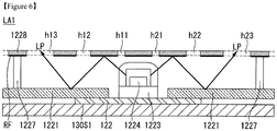
FIG. 6 , alight source 1224 may be mounted on ahousing 1223. Thehousing 1223 may be mounted on thesubstrate 122. Areflection sheet 1221 may be positioned on thesubstrate 122. Thereflection sheet 1221 may partially overlap thesubstrate 122 in order to be adjacent to thelight source 1224 or thehousing 1223. Anoptical sheet 1228 may be positioned over thereflection sheet 1221 and/or thelight source 1224 and/or thesubstrate 122, and may be spaced apart therefrom. That is, an empty space AG may be formed between theoptical sheet 1228 and thereflection sheet 1221. Theoptical sheet 1228 may be spaced apart from thereflection sheet 1221 by asupport 1227. - The
optical sheet 1228 may include a plurality of holes h. The plurality of holes h may be formed to penetrate theoptical sheet 1228. The size of a second hole h12 may be greater than the size of a first hole h11. The size of a third hole h13 may be greater than the size of the second hole h12. That is, the sizes of the plurality of holes h may be greater as the plurality of holes becomes distant in a horizontal direction from thelight source 1224. Accordingly, a light distribution may be uniform regardless of thelight source 1224. - The
optical sheet 1228 may include a reflection surface RF. The reflection surface RF may be formed on the bottom of theoptical sheet 1228. Accordingly, light may be reflected and/or scattered between thereflection sheet 1221 and theoptical sheet 1228. The reflected and/or scattered light may be externally output through the plurality of holes h. The aforementioned contents may be an example of the first light assembly LA1 or a second light assembly LA2. - Referring to
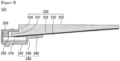
FIGS. 7 and8 , alight source 220 may be mounted on asubstrate 210. For example, thesubstrate 210 may be a PCB. Thelight source 220 may be electrically connected to thesubstrate 210. Thelight source 220 may provide light in the lateral direction of thesubstrate 210. This may be called a side view type. Alight guide panel 230 may be positioned over thesubstrate 210. Thelight source 220 may be positioned on one side of thelight guide panel 230. - The
light guide panel 230 may include anintroduction part 231, aslope portion 232, and alight output portion 233. Theintroduction part 231 may form one side of thelight guide panel 230. Theintroduction part 231 may neighbor thelight source 220 or come into contact with thelight source 220. Theslope portion 232 may form the lower surface of thelight guide panel 230. Theslope portion 232 may have a positive slope with respect to the center of thelight source 220. This may mean that theslope portion 232 may have an ascent slope as it becomes distant from thelight source 220. Thelight output portion 233 may form the upper surface of thelight guide panel 230. Thelight output portion 233 may face theslope portion 232. A steppedportion 234 may be formed between theintroduction part 231 and thelight output portion 233. Theintroduction part 231 may be called alight incidence portion 231. - A
lower cover 240 may be positioned on the lower side of thesubstrate 210 and/or under thelight guide panel 230. Thelower cover 240 may receive thesubstrate 210 and thelight source 220 and support thelight guide panel 230. Thelower cover 240 may include abase 242. The base 242 may be a lengthily elongated flat panel. Thelower cover 240 may include anextension portion 244. Theextension portion 244 may be extended from thelight source 220 to a direction toward thelight guide panel 230. Thebase 242 and theextension portion 244 may form astep 246. Anupper cover 250 may be coupled to thelower cover 240. Theupper cover 250 may press thelight guide panel 230 from the upper side. Theupper cover 250 may cover the top of thelight source 220. For example, theupper cover 250 and thelower cover 240 may be metal. - A
reflection plate 235 may be positioned at the bottom of thelight guide panel 230 or may come into contact with the bottom of thelight guide panel 230 or may be formed on the bottom of thelight guide panel 230. For example, thereflection plate 235 may be a reflection sheet or may be a coated reflection material. - The aforementioned contents may be an example of the first light assembly LA1 or the second light assembly LA2.
- Referring to
FIG. 9 , thelight guide panel 230 may be a plural number. The plurality oflight guide panels 230 may be sequentially arranged. For example, a first light guide panel U1 may be positioned on one side, a second light guide panel U2 may neighbor the first light guide panel U1, a third light guide panel U3 may neighbor the second light guide panel U2, a fourth light guide panel U4 may neighbor the third light guide panel U3, a fifth light guide panel U5 may neighbor the fourth light guide panel U4, and a sixth light guide panel U6 may neighbor the fifth light guide panel U5. A single or a plurality of the light sources 220 (refer toFIG. 7 ) may be arranged in accordance with the light guide panels U1-U6. Accordingly, the amount of light can be locally adjusted. - The aforementioned contents may be an example of the first light assembly LA1 or the second light assembly LA2. The first light assembly LA1 and/or the second light assembly LA2 may be called a side light assembly.
- Referring to
FIG. 10 , the main light assembly LA may be positioned on the bottom 130B of theframe 130. The side light assemblies LA1 and LA2 may include an eleventh light assembly LA11, a twelfth light assembly LA12, a twenty-first light assembly LA21, and a twenty-second light assembly LA22. The eleventh light assembly LA11 and/or the twelfth light assembly LA12 may be positioned on the first side support 130S1. The twenty-first light assembly LA21 and/or the twenty-second light assembly LA22 may be positioned on the second side support 130S2. - A connector CN may be electrically connected to a plurality of the
substrates 122. Externally supplied power may be provided to the light sources LS provided in the main light assembly LA through the plurality ofsubstrates 122. - Referring to
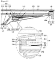
FIG. 11 , theframe 130 may include aflange 130P. Theflange 130P may be formed at one end of the side support 130S1. Theflange 130P may support a side frame SF. Theoptical sheet 125 may be supported by theflange 130P, and may be positioned under thedisplay panel 110. - The side frame SF may include a horizontal portion SF1 and a vertical portion SF2. The vertical portion SF2 may form an external appearance of the display device. An adhesion member AD may be fixed on the horizontal portion SF1, and the
display panel 110 may be fixed to the adhesion member AD. For example, the adhesion member AD may be a double-sided tape. - A reflection sheet 300 may include a
first part 310, asecond part 320, and athird part 330. Thefirst part 310 may be positioned on the bottom 130B of theframe 130. Thefirst part 310 may include a hole (not illustrated) through which thelens 124 passes. Thesecond part 320 may be extended from thefirst part 310 to the side light assembly LA1. Thesecond part 320 may face the stepped portion 130I1. - The
third part 330 may be positioned on the side light assembly LA1. Thethird part 330 may be fixed on theupper cover 250 of the side light assembly LA1. One end of thethird part 330 may be adjacent to the side of the steppedportion 234 of thelight guide panel 230 or may come into contact with the side of the steppedportion 234 of thelight guide panel 230. Thethird part 330 may be coupled to thesecond part 320. Accordingly, a dark area which may be formed between the main light assembly LA and the side light assembly LA1 can be improved, and a light distribution provided to thedisplay panel 110 can be uniform. - Referring to
FIG. 12 , the side support 130S1 may be extended from the bottom 130B to theflange 130P. The side support 130S1 may have a gentle slope from the bottom 130B to theflange 130P. The side light assembly LA1 may be positioned over the side support 130S1. Accordingly, a dark area which may be formed between the main light assembly LA and the side light assembly LA1 can be improved, and a light distribution provided to thedisplay panel 110 can become more uniform. - Referring to
FIG. 13 , thelight source 220 may have many-sided light. Referring toFIG. 13(a) , thelight source 220 may be an LED capable of 5-sided light emission. Referring toFIG. 13(b) , thelight source 220 may be an LED capable of 4-sided light emission. A wall LW may cover one side of thelight source 220. - Referring to
FIGS. 14 and15 , theupper cover 250 may be a plate lengthily elongated in the length direction of one side of thelight guide panel 230. Theupper cover 250 may be coupled to the lower cover 240 (refer toFIG. 7 ) by a fastening member f. Theupper cover 250 may include a light hole LH. A plurality of the light holes LH may be formed in theupper cover 250. The light hole LH may be positioned at the top of the light source 220 (refer toFIG. 7 ). The number of light holes LH may correspond to the number of light sources 220 (refer toFIG. 7 ). - Referring to
FIGS. 16 and17 , light emitted from thelight source 220 to thelight guide panel 230 may pass through theintroduction part 231, may be reflected within thelight guide panel 230, and may be spread to the entirelight guide panel 230. Accordingly, thelight guide panel 230 can uniformly provide light to thedisplay panel 110. Light provided from thelight source 220 to the upper side of thelight source 220 may be provided to thedisplay panel 110 through the light hole LH of theupper cover 250. Accordingly, light having a distribution identical with or similar to that of the main light assembly LA and the side light assembly LA1 can be provided between the main light assembly LA and the side light assembly LA1. - Any or others of the aforementioned embodiments of the disclosure should not be understood to be exclusive or different. In any or others of the aforementioned embodiments of the disclosure, the elements or functions may be interchangeably used or used in combination.
- The detailed description should not be construed as being limited, but should be considered to be illustrative from all aspects. The scope of the disclosure should be determined by reasonable analysis of the attached claims, and all changes within the equivalent scope of the disclosure are included in the scope of the disclosure.
Claims (10)
- A display device, comprising:a display panel;a frame positioned at a back of the display panel;a main light assembly positioned on the frame between the display panel and the frame; anda side light assembly positioned on the frame between the display panel and the frame and positioned to be adjacent to the main light assembly,wherein the frame comprises a bottom forming a lower surface and a side support extended from the bottom to one side of the display panel,wherein the side support is closer to the display panel than the bottom,wherein the main light assembly is positioned at the bottom, andwherein the side light assembly is positioned at the side support.
- The display device of claim 1,
wherein the main light assembly comprises:a substrate positioned on the bottom;a plurality of light sources sequentially mounted on the substrate; anda plurality of lenses mounted on the substrate and corresponding to the plurality of light sources, respectively. - The display device of claim 1,
wherein the side light assembly comprises:a light guide panel positioned between the display panel and the side support;a light source positioned adjacent to one side surface of the light guide panel; anda reflection plate positioned at a bottom of the light guide panel. - The display device of claim 3,
wherein the light guide panel comprises:a light incidence portion positioned to neighbor the light source;a light output portion forming a top of the light guide panel; anda slope portion forming a bottom of the light guide panel and having a distance closer to the light output portion as the slope portion becomes distant from the light source. - The display device of claim 4,
wherein the reflection plate is bonded to the slope portion. - The display device of claim 4, further comprising:a substrate on which the light source is mounted;a lower cover positioned on a lower side of the substrate; andan upper cover positioned on an upper side of the light source and coupled to the lower cover,wherein the lower cover comprises:a base supporting the substrate; andan extension portion extended from the base to the light guide panel and supporting the light guide panel.
- The display device of claim 6,
wherein the upper cover comprises a light hole formed at a top of the light source, and
wherein the light source provides light toward at least the upper cover. - The display device of claim 2, further comprising:a reflection sheet positioned between the main light assembly and the display panel,wherein the reflection sheet comprises:a first part positioned on the bottom or the substrate;a second part extended from the first part to the side light assembly; anda third part elongated from the second part and covering a part of the side light assembly.
- The display device of claim 1,
wherein the frame further comprises a stepped portion formed between the bottom and the side support. - The display device of claim 1,
wherein the side support comprises:a first side support positioned on one side of the bottom; anda second side support positioned on the other side of the bottom,wherein the side light assembly comprises:a first side light assembly positioned on the first side support; anda second side light assembly positioned on the second side support.
Applications Claiming Priority (2)
| Application Number | Priority Date | Filing Date | Title |
|---|---|---|---|
| KR1020170100371A KR102314920B1 (en) | 2017-08-08 | 2017-08-08 | Display device |
| PCT/KR2018/004512 WO2019031684A1 (en) | 2017-08-08 | 2018-04-18 | Display device |
Publications (3)
| Publication Number | Publication Date |
|---|---|
| EP3667406A1 true EP3667406A1 (en) | 2020-06-17 |
| EP3667406A4 EP3667406A4 (en) | 2021-04-07 |
| EP3667406B1 EP3667406B1 (en) | 2025-07-16 |
Family
ID=65271606
Family Applications (1)
| Application Number | Title | Priority Date | Filing Date |
|---|---|---|---|
| EP18844889.8A Active EP3667406B1 (en) | 2017-08-08 | 2018-04-18 | Display device |
Country Status (4)
| Country | Link |
|---|---|
| US (1) | US10816719B2 (en) |
| EP (1) | EP3667406B1 (en) |
| KR (1) | KR102314920B1 (en) |
| WO (1) | WO2019031684A1 (en) |
Families Citing this family (2)
| Publication number | Priority date | Publication date | Assignee | Title |
|---|---|---|---|---|
| US11543690B2 (en) * | 2020-10-23 | 2023-01-03 | Lg Electronics Inc. | Display device |
| EP4517415A4 (en) * | 2022-09-22 | 2025-08-06 | Lg Electronics Inc | DISPLAY DEVICE |
Family Cites Families (9)
| Publication number | Priority date | Publication date | Assignee | Title |
|---|---|---|---|---|
| KR100654220B1 (en) | 1999-08-03 | 2006-12-05 | 삼성전자주식회사 | LCD Display |
| KR20090008749U (en) * | 2008-02-26 | 2009-08-31 | 주식회사 자화라이텍 | Side light type led lightening device having auxiliary led in direct type for auxiliary display |
| CN102128398B (en) * | 2011-03-21 | 2013-05-01 | 深圳市华星光电技术有限公司 | Backlight module and liquid crystal display device |
| CN202253209U (en) * | 2011-10-14 | 2012-05-30 | 深圳市华星光电技术有限公司 | Backlight module and liquid crystal display comprising same |
| KR101470057B1 (en) * | 2011-10-27 | 2014-12-10 | 엘지이노텍 주식회사 | optical assembly, backlight unit having the same, and display apparatus thereof |
| KR101474734B1 (en) | 2013-06-03 | 2014-12-22 | 삼성전자주식회사 | Illuminating apparatus and liquid crystal display having the same |
| CN104100886B (en) | 2014-06-30 | 2016-08-03 | 北京京东方视讯科技有限公司 | A kind of backlight, display device and method for controlling backlight thereof thereof |
| CN104864311A (en) * | 2015-05-06 | 2015-08-26 | 广州创维平面显示科技有限公司 | Liquid crystal display device and downright and side entry hybrid backlight module |
| KR102339539B1 (en) * | 2015-05-08 | 2021-12-16 | 삼성전자주식회사 | Display apparatus |
-
2017
- 2017-08-08 KR KR1020170100371A patent/KR102314920B1/en active Active
-
2018
- 2018-04-18 EP EP18844889.8A patent/EP3667406B1/en active Active
- 2018-04-18 WO PCT/KR2018/004512 patent/WO2019031684A1/en not_active Ceased
- 2018-04-18 US US16/636,893 patent/US10816719B2/en active Active
Also Published As
| Publication number | Publication date |
|---|---|
| KR102314920B1 (en) | 2021-10-20 |
| US20200166695A1 (en) | 2020-05-28 |
| EP3667406A4 (en) | 2021-04-07 |
| EP3667406B1 (en) | 2025-07-16 |
| KR20190016305A (en) | 2019-02-18 |
| WO2019031684A1 (en) | 2019-02-14 |
| US10816719B2 (en) | 2020-10-27 |
Similar Documents
| Publication | Publication Date | Title |
|---|---|---|
| KR102504803B1 (en) | Display device | |
| KR102650102B1 (en) | Display device | |
| KR102558277B1 (en) | Display device | |
| KR100959157B1 (en) | Multi-screen device with multiple display panels | |
| EP3825761B1 (en) | Display device | |
| KR102466114B1 (en) | Display device | |
| KR102557654B1 (en) | Display device | |
| KR102585211B1 (en) | Display device | |
| EP3761108B1 (en) | Display device | |
| KR102370820B1 (en) | Display device | |
| KR20160081599A (en) | Back light unit and display apparatus having it | |
| CN218767715U (en) | Display device | |
| KR102476297B1 (en) | Display device | |
| EP2546685B1 (en) | Backlight unit and display apparatus using the same | |
| US9116277B2 (en) | Lighting device, display device, and television receiver | |
| US20190254195A1 (en) | Display device | |
| EP3667406B1 (en) | Display device | |
| KR102547734B1 (en) | Display device | |
| EP3559733B1 (en) | Display apparatus | |
| KR102104980B1 (en) | Liquid Crystal Display | |
| KR20190116836A (en) | Display device | |
| KR20160078038A (en) | Display apparatus | |
| US20260010037A1 (en) | Display device | |
| KR101666224B1 (en) | Backlight unit and liquid crystal display device having the same | |
| KR20070073505A (en) | Backlight unit and liquid crystal display including the same |
Legal Events
| Date | Code | Title | Description |
|---|---|---|---|
| STAA | Information on the status of an ep patent application or granted ep patent |
Free format text: STATUS: THE INTERNATIONAL PUBLICATION HAS BEEN MADE |
|
| PUAI | Public reference made under article 153(3) epc to a published international application that has entered the european phase |
Free format text: ORIGINAL CODE: 0009012 |
|
| STAA | Information on the status of an ep patent application or granted ep patent |
Free format text: STATUS: REQUEST FOR EXAMINATION WAS MADE |
|
| 17P | Request for examination filed |
Effective date: 20200308 |
|
| AK | Designated contracting states |
Kind code of ref document: A1 Designated state(s): AL AT BE BG CH CY CZ DE DK EE ES FI FR GB GR HR HU IE IS IT LI LT LU LV MC MK MT NL NO PL PT RO RS SE SI SK SM TR |
|
| AX | Request for extension of the european patent |
Extension state: BA ME |
|
| DAV | Request for validation of the european patent (deleted) | ||
| DAX | Request for extension of the european patent (deleted) | ||
| A4 | Supplementary search report drawn up and despatched |
Effective date: 20210309 |
|
| RIC1 | Information provided on ipc code assigned before grant |
Ipc: G02F 1/13357 20060101ALI20210302BHEP Ipc: G02F 1/1335 20060101AFI20210302BHEP Ipc: F21V 8/00 20060101ALI20210302BHEP |
|
| STAA | Information on the status of an ep patent application or granted ep patent |
Free format text: STATUS: EXAMINATION IS IN PROGRESS |
|
| 17Q | First examination report despatched |
Effective date: 20230213 |
|
| GRAP | Despatch of communication of intention to grant a patent |
Free format text: ORIGINAL CODE: EPIDOSNIGR1 |
|
| STAA | Information on the status of an ep patent application or granted ep patent |
Free format text: STATUS: GRANT OF PATENT IS INTENDED |
|
| INTG | Intention to grant announced |
Effective date: 20250211 |
|
| GRAS | Grant fee paid |
Free format text: ORIGINAL CODE: EPIDOSNIGR3 |
|
| GRAA | (expected) grant |
Free format text: ORIGINAL CODE: 0009210 |
|
| STAA | Information on the status of an ep patent application or granted ep patent |
Free format text: STATUS: THE PATENT HAS BEEN GRANTED |
|
| AK | Designated contracting states |
Kind code of ref document: B1 Designated state(s): AL AT BE BG CH CY CZ DE DK EE ES FI FR GB GR HR HU IE IS IT LI LT LU LV MC MK MT NL NO PL PT RO RS SE SI SK SM TR |
|
| REG | Reference to a national code |
Ref country code: GB Ref legal event code: FG4D |
|
| REG | Reference to a national code |
Ref country code: CH Ref legal event code: EP |
|
| REG | Reference to a national code |
Ref country code: DE Ref legal event code: R096 Ref document number: 602018083685 Country of ref document: DE |
|
| REG | Reference to a national code |
Ref country code: IE Ref legal event code: FG4D |
|
| REG | Reference to a national code |
Ref country code: NL Ref legal event code: MP Effective date: 20250716 |
|
| PG25 | Lapsed in a contracting state [announced via postgrant information from national office to epo] |
Ref country code: PT Free format text: LAPSE BECAUSE OF FAILURE TO SUBMIT A TRANSLATION OF THE DESCRIPTION OR TO PAY THE FEE WITHIN THE PRESCRIBED TIME-LIMIT Effective date: 20251117 |
|
| PG25 | Lapsed in a contracting state [announced via postgrant information from national office to epo] |
Ref country code: NL Free format text: LAPSE BECAUSE OF FAILURE TO SUBMIT A TRANSLATION OF THE DESCRIPTION OR TO PAY THE FEE WITHIN THE PRESCRIBED TIME-LIMIT Effective date: 20250716 |
|
| REG | Reference to a national code |
Ref country code: AT Ref legal event code: MK05 Ref document number: 1814557 Country of ref document: AT Kind code of ref document: T Effective date: 20250716 |
|
| PG25 | Lapsed in a contracting state [announced via postgrant information from national office to epo] |
Ref country code: IS Free format text: LAPSE BECAUSE OF FAILURE TO SUBMIT A TRANSLATION OF THE DESCRIPTION OR TO PAY THE FEE WITHIN THE PRESCRIBED TIME-LIMIT Effective date: 20251116 |
|
| PG25 | Lapsed in a contracting state [announced via postgrant information from national office to epo] |
Ref country code: NO Free format text: LAPSE BECAUSE OF FAILURE TO SUBMIT A TRANSLATION OF THE DESCRIPTION OR TO PAY THE FEE WITHIN THE PRESCRIBED TIME-LIMIT Effective date: 20251016 |
|
| REG | Reference to a national code |
Ref country code: LT Ref legal event code: MG9D |
|
| PG25 | Lapsed in a contracting state [announced via postgrant information from national office to epo] |
Ref country code: AT Free format text: LAPSE BECAUSE OF FAILURE TO SUBMIT A TRANSLATION OF THE DESCRIPTION OR TO PAY THE FEE WITHIN THE PRESCRIBED TIME-LIMIT Effective date: 20250716 |
|
| PG25 | Lapsed in a contracting state [announced via postgrant information from national office to epo] |
Ref country code: FI Free format text: LAPSE BECAUSE OF FAILURE TO SUBMIT A TRANSLATION OF THE DESCRIPTION OR TO PAY THE FEE WITHIN THE PRESCRIBED TIME-LIMIT Effective date: 20250716 |
|
| PG25 | Lapsed in a contracting state [announced via postgrant information from national office to epo] |
Ref country code: HR Free format text: LAPSE BECAUSE OF FAILURE TO SUBMIT A TRANSLATION OF THE DESCRIPTION OR TO PAY THE FEE WITHIN THE PRESCRIBED TIME-LIMIT Effective date: 20250716 |
|
| PG25 | Lapsed in a contracting state [announced via postgrant information from national office to epo] |
Ref country code: GR Free format text: LAPSE BECAUSE OF FAILURE TO SUBMIT A TRANSLATION OF THE DESCRIPTION OR TO PAY THE FEE WITHIN THE PRESCRIBED TIME-LIMIT Effective date: 20251017 |
|
| PG25 | Lapsed in a contracting state [announced via postgrant information from national office to epo] |
Ref country code: SE Free format text: LAPSE BECAUSE OF FAILURE TO SUBMIT A TRANSLATION OF THE DESCRIPTION OR TO PAY THE FEE WITHIN THE PRESCRIBED TIME-LIMIT Effective date: 20250716 |
|
| PG25 | Lapsed in a contracting state [announced via postgrant information from national office to epo] |
Ref country code: LV Free format text: LAPSE BECAUSE OF FAILURE TO SUBMIT A TRANSLATION OF THE DESCRIPTION OR TO PAY THE FEE WITHIN THE PRESCRIBED TIME-LIMIT Effective date: 20250716 |
|
| PG25 | Lapsed in a contracting state [announced via postgrant information from national office to epo] |
Ref country code: PL Free format text: LAPSE BECAUSE OF FAILURE TO SUBMIT A TRANSLATION OF THE DESCRIPTION OR TO PAY THE FEE WITHIN THE PRESCRIBED TIME-LIMIT Effective date: 20250716 Ref country code: BG Free format text: LAPSE BECAUSE OF FAILURE TO SUBMIT A TRANSLATION OF THE DESCRIPTION OR TO PAY THE FEE WITHIN THE PRESCRIBED TIME-LIMIT Effective date: 20250716 |
|
| PG25 | Lapsed in a contracting state [announced via postgrant information from national office to epo] |
Ref country code: RS Free format text: LAPSE BECAUSE OF FAILURE TO SUBMIT A TRANSLATION OF THE DESCRIPTION OR TO PAY THE FEE WITHIN THE PRESCRIBED TIME-LIMIT Effective date: 20251016 |
|
| PG25 | Lapsed in a contracting state [announced via postgrant information from national office to epo] |
Ref country code: ES Free format text: LAPSE BECAUSE OF FAILURE TO SUBMIT A TRANSLATION OF THE DESCRIPTION OR TO PAY THE FEE WITHIN THE PRESCRIBED TIME-LIMIT Effective date: 20250716 |
|
| PG25 | Lapsed in a contracting state [announced via postgrant information from national office to epo] |
Ref country code: SM Free format text: LAPSE BECAUSE OF FAILURE TO SUBMIT A TRANSLATION OF THE DESCRIPTION OR TO PAY THE FEE WITHIN THE PRESCRIBED TIME-LIMIT Effective date: 20250716 |
|
| PGFP | Annual fee paid to national office [announced via postgrant information from national office to epo] |
Ref country code: GB Payment date: 20260309 Year of fee payment: 9 |
|
| PG25 | Lapsed in a contracting state [announced via postgrant information from national office to epo] |
Ref country code: DK Free format text: LAPSE BECAUSE OF FAILURE TO SUBMIT A TRANSLATION OF THE DESCRIPTION OR TO PAY THE FEE WITHIN THE PRESCRIBED TIME-LIMIT Effective date: 20250716 |
|
| PG25 | Lapsed in a contracting state [announced via postgrant information from national office to epo] |
Ref country code: IT Free format text: LAPSE BECAUSE OF FAILURE TO SUBMIT A TRANSLATION OF THE DESCRIPTION OR TO PAY THE FEE WITHIN THE PRESCRIBED TIME-LIMIT Effective date: 20250716 |
|
| PGFP | Annual fee paid to national office [announced via postgrant information from national office to epo] |
Ref country code: FR Payment date: 20260309 Year of fee payment: 9 |
|
| PG25 | Lapsed in a contracting state [announced via postgrant information from national office to epo] |
Ref country code: CZ Free format text: LAPSE BECAUSE OF FAILURE TO SUBMIT A TRANSLATION OF THE DESCRIPTION OR TO PAY THE FEE WITHIN THE PRESCRIBED TIME-LIMIT Effective date: 20250716 |
|
| PG25 | Lapsed in a contracting state [announced via postgrant information from national office to epo] |
Ref country code: SK Free format text: LAPSE BECAUSE OF FAILURE TO SUBMIT A TRANSLATION OF THE DESCRIPTION OR TO PAY THE FEE WITHIN THE PRESCRIBED TIME-LIMIT Effective date: 20250716 Ref country code: EE Free format text: LAPSE BECAUSE OF FAILURE TO SUBMIT A TRANSLATION OF THE DESCRIPTION OR TO PAY THE FEE WITHIN THE PRESCRIBED TIME-LIMIT Effective date: 20250716 |