EP3665015B1 - Printing system and writing module thereof - Google Patents
Printing system and writing module thereof Download PDFInfo
- Publication number
- EP3665015B1 EP3665015B1 EP18762930.8A EP18762930A EP3665015B1 EP 3665015 B1 EP3665015 B1 EP 3665015B1 EP 18762930 A EP18762930 A EP 18762930A EP 3665015 B1 EP3665015 B1 EP 3665015B1
- Authority
- EP
- European Patent Office
- Prior art keywords
- imaging surface
- light
- polymer
- printing
- printing system
- Prior art date
- Legal status (The legal status is an assumption and is not a legal conclusion. Google has not performed a legal analysis and makes no representation as to the accuracy of the status listed.)
- Active
Links
Images



Classifications
-
- B—PERFORMING OPERATIONS; TRANSPORTING
- B29—WORKING OF PLASTICS; WORKING OF SUBSTANCES IN A PLASTIC STATE IN GENERAL
- B29C—SHAPING OR JOINING OF PLASTICS; SHAPING OF MATERIAL IN A PLASTIC STATE, NOT OTHERWISE PROVIDED FOR; AFTER-TREATMENT OF THE SHAPED PRODUCTS, e.g. REPAIRING
- B29C64/00—Additive manufacturing, i.e. manufacturing of three-dimensional [3D] objects by additive deposition, additive agglomeration or additive layering, e.g. by 3D printing, stereolithography or selective laser sintering
- B29C64/20—Apparatus for additive manufacturing; Details thereof or accessories therefor
- B29C64/264—Arrangements for irradiation
- B29C64/268—Arrangements for irradiation using laser beams; using electron beams [EB]
-
- B—PERFORMING OPERATIONS; TRANSPORTING
- B33—ADDITIVE MANUFACTURING TECHNOLOGY
- B33Y—ADDITIVE MANUFACTURING, i.e. MANUFACTURING OF THREE-DIMENSIONAL [3D] OBJECTS BY ADDITIVE DEPOSITION, ADDITIVE AGGLOMERATION OR ADDITIVE LAYERING, e.g. BY 3D PRINTING, STEREOLITHOGRAPHY OR SELECTIVE LASER SINTERING
- B33Y30/00—Apparatus for additive manufacturing; Details thereof or accessories therefor
-
- B—PERFORMING OPERATIONS; TRANSPORTING
- B41—PRINTING; LINING MACHINES; TYPEWRITERS; STAMPS
- B41J—TYPEWRITERS; SELECTIVE PRINTING MECHANISMS, i.e. MECHANISMS PRINTING OTHERWISE THAN FROM A FORME; CORRECTION OF TYPOGRAPHICAL ERRORS
- B41J2/00—Typewriters or selective printing mechanisms characterised by the printing or marking process for which they are designed
- B41J2/005—Typewriters or selective printing mechanisms characterised by the printing or marking process for which they are designed characterised by bringing liquid or particles selectively into contact with a printing material
- B41J2/0057—Typewriters or selective printing mechanisms characterised by the printing or marking process for which they are designed characterised by bringing liquid or particles selectively into contact with a printing material where an intermediate transfer member receives the ink before transferring it on the printing material
-
- B—PERFORMING OPERATIONS; TRANSPORTING
- B41—PRINTING; LINING MACHINES; TYPEWRITERS; STAMPS
- B41J—TYPEWRITERS; SELECTIVE PRINTING MECHANISMS, i.e. MECHANISMS PRINTING OTHERWISE THAN FROM A FORME; CORRECTION OF TYPOGRAPHICAL ERRORS
- B41J2/00—Typewriters or selective printing mechanisms characterised by the printing or marking process for which they are designed
- B41J2/435—Typewriters or selective printing mechanisms characterised by the printing or marking process for which they are designed characterised by selective application of radiation to a printing material or impression-transfer material
- B41J2/447—Typewriters or selective printing mechanisms characterised by the printing or marking process for which they are designed characterised by selective application of radiation to a printing material or impression-transfer material using arrays of radiation sources
-
- B—PERFORMING OPERATIONS; TRANSPORTING
- B41—PRINTING; LINING MACHINES; TYPEWRITERS; STAMPS
- B41J—TYPEWRITERS; SELECTIVE PRINTING MECHANISMS, i.e. MECHANISMS PRINTING OTHERWISE THAN FROM A FORME; CORRECTION OF TYPOGRAPHICAL ERRORS
- B41J2/00—Typewriters or selective printing mechanisms characterised by the printing or marking process for which they are designed
- B41J2/435—Typewriters or selective printing mechanisms characterised by the printing or marking process for which they are designed characterised by selective application of radiation to a printing material or impression-transfer material
- B41J2/447—Typewriters or selective printing mechanisms characterised by the printing or marking process for which they are designed characterised by selective application of radiation to a printing material or impression-transfer material using arrays of radiation sources
- B41J2/45—Typewriters or selective printing mechanisms characterised by the printing or marking process for which they are designed characterised by selective application of radiation to a printing material or impression-transfer material using arrays of radiation sources using light-emitting diode [LED] or laser arrays
-
- B—PERFORMING OPERATIONS; TRANSPORTING
- B41—PRINTING; LINING MACHINES; TYPEWRITERS; STAMPS
- B41J—TYPEWRITERS; SELECTIVE PRINTING MECHANISMS, i.e. MECHANISMS PRINTING OTHERWISE THAN FROM A FORME; CORRECTION OF TYPOGRAPHICAL ERRORS
- B41J2/00—Typewriters or selective printing mechanisms characterised by the printing or marking process for which they are designed
- B41J2/435—Typewriters or selective printing mechanisms characterised by the printing or marking process for which they are designed characterised by selective application of radiation to a printing material or impression-transfer material
- B41J2/447—Typewriters or selective printing mechanisms characterised by the printing or marking process for which they are designed characterised by selective application of radiation to a printing material or impression-transfer material using arrays of radiation sources
- B41J2/455—Typewriters or selective printing mechanisms characterised by the printing or marking process for which they are designed characterised by selective application of radiation to a printing material or impression-transfer material using arrays of radiation sources using laser arrays, the laser array being smaller than the medium to be recorded
-
- B—PERFORMING OPERATIONS; TRANSPORTING
- B41—PRINTING; LINING MACHINES; TYPEWRITERS; STAMPS
- B41M—PRINTING, DUPLICATING, MARKING, OR COPYING PROCESSES; COLOUR PRINTING
- B41M5/00—Duplicating or marking methods; Sheet materials for use therein
- B41M5/025—Duplicating or marking methods; Sheet materials for use therein by transferring ink from the master sheet
-
- B—PERFORMING OPERATIONS; TRANSPORTING
- B41—PRINTING; LINING MACHINES; TYPEWRITERS; STAMPS
- B41M—PRINTING, DUPLICATING, MARKING, OR COPYING PROCESSES; COLOUR PRINTING
- B41M5/00—Duplicating or marking methods; Sheet materials for use therein
- B41M5/025—Duplicating or marking methods; Sheet materials for use therein by transferring ink from the master sheet
- B41M5/0256—Duplicating or marking methods; Sheet materials for use therein by transferring ink from the master sheet the transferable ink pattern being obtained by means of a computer driven printer, e.g. an ink jet or laser printer, or by electrographic means
-
- B—PERFORMING OPERATIONS; TRANSPORTING
- B41—PRINTING; LINING MACHINES; TYPEWRITERS; STAMPS
- B41M—PRINTING, DUPLICATING, MARKING, OR COPYING PROCESSES; COLOUR PRINTING
- B41M5/00—Duplicating or marking methods; Sheet materials for use therein
- B41M5/025—Duplicating or marking methods; Sheet materials for use therein by transferring ink from the master sheet
- B41M5/03—Duplicating or marking methods; Sheet materials for use therein by transferring ink from the master sheet by pressure
-
- G—PHYSICS
- G02—OPTICS
- G02B—OPTICAL ELEMENTS, SYSTEMS OR APPARATUS
- G02B19/00—Condensers, e.g. light collectors or similar non-imaging optics
- G02B19/0004—Condensers, e.g. light collectors or similar non-imaging optics characterised by the optical means employed
- G02B19/0009—Condensers, e.g. light collectors or similar non-imaging optics characterised by the optical means employed having refractive surfaces only
-
- G—PHYSICS
- G02—OPTICS
- G02B—OPTICAL ELEMENTS, SYSTEMS OR APPARATUS
- G02B19/00—Condensers, e.g. light collectors or similar non-imaging optics
- G02B19/0033—Condensers, e.g. light collectors or similar non-imaging optics characterised by the use
- G02B19/0047—Condensers, e.g. light collectors or similar non-imaging optics characterised by the use for use with a light source
-
- G—PHYSICS
- G02—OPTICS
- G02B—OPTICAL ELEMENTS, SYSTEMS OR APPARATUS
- G02B3/00—Simple or compound lenses
- G02B3/0087—Simple or compound lenses with index gradient
-
- G—PHYSICS
- G02—OPTICS
- G02B—OPTICAL ELEMENTS, SYSTEMS OR APPARATUS
- G02B3/00—Simple or compound lenses
- G02B3/02—Simple or compound lenses with non-spherical faces
- G02B3/06—Simple or compound lenses with non-spherical faces with cylindrical or toric faces
-
- G—PHYSICS
- G03—PHOTOGRAPHY; CINEMATOGRAPHY; ANALOGOUS TECHNIQUES USING WAVES OTHER THAN OPTICAL WAVES; ELECTROGRAPHY; HOLOGRAPHY
- G03G—ELECTROGRAPHY; ELECTROPHOTOGRAPHY; MAGNETOGRAPHY
- G03G15/00—Apparatus for electrographic processes using a charge pattern
- G03G15/01—Apparatus for electrographic processes using a charge pattern for producing multicoloured copies
- G03G15/0142—Structure of complete machines
- G03G15/0178—Structure of complete machines using more than one reusable electrographic recording member, e.g. one for every monocolour image
-
- G—PHYSICS
- G03—PHOTOGRAPHY; CINEMATOGRAPHY; ANALOGOUS TECHNIQUES USING WAVES OTHER THAN OPTICAL WAVES; ELECTROGRAPHY; HOLOGRAPHY
- G03G—ELECTROGRAPHY; ELECTROPHOTOGRAPHY; MAGNETOGRAPHY
- G03G15/00—Apparatus for electrographic processes using a charge pattern
- G03G15/04—Apparatus for electrographic processes using a charge pattern for exposing, i.e. imagewise exposure by optically projecting the original image on a photoconductive recording material
- G03G15/04036—Details of illuminating systems, e.g. lamps, reflectors
- G03G15/04045—Details of illuminating systems, e.g. lamps, reflectors for exposing image information provided otherwise than by directly projecting the original image onto the photoconductive recording material, e.g. digital copiers
- G03G15/04072—Details of illuminating systems, e.g. lamps, reflectors for exposing image information provided otherwise than by directly projecting the original image onto the photoconductive recording material, e.g. digital copiers by laser
-
- G—PHYSICS
- G03—PHOTOGRAPHY; CINEMATOGRAPHY; ANALOGOUS TECHNIQUES USING WAVES OTHER THAN OPTICAL WAVES; ELECTROGRAPHY; HOLOGRAPHY
- G03G—ELECTROGRAPHY; ELECTROPHOTOGRAPHY; MAGNETOGRAPHY
- G03G15/00—Apparatus for electrographic processes using a charge pattern
- G03G15/06—Apparatus for electrographic processes using a charge pattern for developing
- G03G15/10—Apparatus for electrographic processes using a charge pattern for developing using a liquid developer
-
- G—PHYSICS
- G03—PHOTOGRAPHY; CINEMATOGRAPHY; ANALOGOUS TECHNIQUES USING WAVES OTHER THAN OPTICAL WAVES; ELECTROGRAPHY; HOLOGRAPHY
- G03G—ELECTROGRAPHY; ELECTROPHOTOGRAPHY; MAGNETOGRAPHY
- G03G15/00—Apparatus for electrographic processes using a charge pattern
- G03G15/22—Apparatus for electrographic processes using a charge pattern involving the combination of more than one step according to groups G03G13/02 - G03G13/20
- G03G15/34—Apparatus for electrographic processes using a charge pattern involving the combination of more than one step according to groups G03G13/02 - G03G13/20 in which the powder image is formed directly on the recording material, e.g. by using a liquid toner
- G03G15/342—Apparatus for electrographic processes using a charge pattern involving the combination of more than one step according to groups G03G13/02 - G03G13/20 in which the powder image is formed directly on the recording material, e.g. by using a liquid toner by forming a uniform powder layer and then removing the non-image areas
-
- H—ELECTRICITY
- H01—ELECTRIC ELEMENTS
- H01S—DEVICES USING THE PROCESS OF LIGHT AMPLIFICATION BY STIMULATED EMISSION OF RADIATION [LASER] TO AMPLIFY OR GENERATE LIGHT; DEVICES USING STIMULATED EMISSION OF ELECTROMAGNETIC RADIATION IN WAVE RANGES OTHER THAN OPTICAL
- H01S5/00—Semiconductor lasers
- H01S5/02—Structural details or components not essential to laser action
- H01S5/024—Arrangements for thermal management
- H01S5/02469—Passive cooling, e.g. where heat is removed by the housing as a whole or by a heat pipe without any active cooling element like a TEC
-
- H—ELECTRICITY
- H01—ELECTRIC ELEMENTS
- H01S—DEVICES USING THE PROCESS OF LIGHT AMPLIFICATION BY STIMULATED EMISSION OF RADIATION [LASER] TO AMPLIFY OR GENERATE LIGHT; DEVICES USING STIMULATED EMISSION OF ELECTROMAGNETIC RADIATION IN WAVE RANGES OTHER THAN OPTICAL
- H01S5/00—Semiconductor lasers
- H01S5/10—Construction or shape of the optical resonator, e.g. extended or external cavity, coupled cavities, bent-guide, varying width, thickness or composition of the active region
- H01S5/18—Surface-emitting [SE] lasers, e.g. having both horizontal and vertical cavities
- H01S5/183—Surface-emitting [SE] lasers, e.g. having both horizontal and vertical cavities having only vertical cavities, e.g. vertical cavity surface-emitting lasers [VCSEL]
- H01S5/18308—Surface-emitting [SE] lasers, e.g. having both horizontal and vertical cavities having only vertical cavities, e.g. vertical cavity surface-emitting lasers [VCSEL] having a special structure for lateral current or light confinement
- H01S5/18311—Surface-emitting [SE] lasers, e.g. having both horizontal and vertical cavities having only vertical cavities, e.g. vertical cavity surface-emitting lasers [VCSEL] having a special structure for lateral current or light confinement using selective oxidation
-
- H—ELECTRICITY
- H01—ELECTRIC ELEMENTS
- H01S—DEVICES USING THE PROCESS OF LIGHT AMPLIFICATION BY STIMULATED EMISSION OF RADIATION [LASER] TO AMPLIFY OR GENERATE LIGHT; DEVICES USING STIMULATED EMISSION OF ELECTROMAGNETIC RADIATION IN WAVE RANGES OTHER THAN OPTICAL
- H01S5/00—Semiconductor lasers
- H01S5/40—Arrangement of two or more semiconductor lasers, not provided for in groups H01S5/02 - H01S5/30
- H01S5/42—Arrays of surface emitting lasers
- H01S5/423—Arrays of surface emitting lasers having a vertical cavity
-
- H—ELECTRICITY
- H01—ELECTRIC ELEMENTS
- H01S—DEVICES USING THE PROCESS OF LIGHT AMPLIFICATION BY STIMULATED EMISSION OF RADIATION [LASER] TO AMPLIFY OR GENERATE LIGHT; DEVICES USING STIMULATED EMISSION OF ELECTROMAGNETIC RADIATION IN WAVE RANGES OTHER THAN OPTICAL
- H01S5/00—Semiconductor lasers
- H01S5/40—Arrangement of two or more semiconductor lasers, not provided for in groups H01S5/02 - H01S5/30
- H01S5/42—Arrays of surface emitting lasers
- H01S5/423—Arrays of surface emitting lasers having a vertical cavity
- H01S5/426—Vertically stacked cavities
-
- H—ELECTRICITY
- H01—ELECTRIC ELEMENTS
- H01S—DEVICES USING THE PROCESS OF LIGHT AMPLIFICATION BY STIMULATED EMISSION OF RADIATION [LASER] TO AMPLIFY OR GENERATE LIGHT; DEVICES USING STIMULATED EMISSION OF ELECTROMAGNETIC RADIATION IN WAVE RANGES OTHER THAN OPTICAL
- H01S5/00—Semiconductor lasers
- H01S5/10—Construction or shape of the optical resonator, e.g. extended or external cavity, coupled cavities, bent-guide, varying width, thickness or composition of the active region
- H01S5/18—Surface-emitting [SE] lasers, e.g. having both horizontal and vertical cavities
- H01S5/183—Surface-emitting [SE] lasers, e.g. having both horizontal and vertical cavities having only vertical cavities, e.g. vertical cavity surface-emitting lasers [VCSEL]
- H01S5/18308—Surface-emitting [SE] lasers, e.g. having both horizontal and vertical cavities having only vertical cavities, e.g. vertical cavity surface-emitting lasers [VCSEL] having a special structure for lateral current or light confinement
- H01S5/18322—Position of the structure
- H01S5/1833—Position of the structure with more than one structure
-
- H—ELECTRICITY
- H01—ELECTRIC ELEMENTS
- H01S—DEVICES USING THE PROCESS OF LIGHT AMPLIFICATION BY STIMULATED EMISSION OF RADIATION [LASER] TO AMPLIFY OR GENERATE LIGHT; DEVICES USING STIMULATED EMISSION OF ELECTROMAGNETIC RADIATION IN WAVE RANGES OTHER THAN OPTICAL
- H01S5/00—Semiconductor lasers
- H01S5/10—Construction or shape of the optical resonator, e.g. extended or external cavity, coupled cavities, bent-guide, varying width, thickness or composition of the active region
- H01S5/18—Surface-emitting [SE] lasers, e.g. having both horizontal and vertical cavities
- H01S5/183—Surface-emitting [SE] lasers, e.g. having both horizontal and vertical cavities having only vertical cavities, e.g. vertical cavity surface-emitting lasers [VCSEL]
- H01S5/18383—Surface-emitting [SE] lasers, e.g. having both horizontal and vertical cavities having only vertical cavities, e.g. vertical cavity surface-emitting lasers [VCSEL] with periodic active regions at nodes or maxima of light intensity
-
- H—ELECTRICITY
- H01—ELECTRIC ELEMENTS
- H01S—DEVICES USING THE PROCESS OF LIGHT AMPLIFICATION BY STIMULATED EMISSION OF RADIATION [LASER] TO AMPLIFY OR GENERATE LIGHT; DEVICES USING STIMULATED EMISSION OF ELECTROMAGNETIC RADIATION IN WAVE RANGES OTHER THAN OPTICAL
- H01S5/00—Semiconductor lasers
- H01S5/10—Construction or shape of the optical resonator, e.g. extended or external cavity, coupled cavities, bent-guide, varying width, thickness or composition of the active region
- H01S5/18—Surface-emitting [SE] lasers, e.g. having both horizontal and vertical cavities
- H01S5/183—Surface-emitting [SE] lasers, e.g. having both horizontal and vertical cavities having only vertical cavities, e.g. vertical cavity surface-emitting lasers [VCSEL]
- H01S5/18397—Plurality of active layers vertically stacked in a cavity for multi-wavelength emission
-
- H—ELECTRICITY
- H01—ELECTRIC ELEMENTS
- H01S—DEVICES USING THE PROCESS OF LIGHT AMPLIFICATION BY STIMULATED EMISSION OF RADIATION [LASER] TO AMPLIFY OR GENERATE LIGHT; DEVICES USING STIMULATED EMISSION OF ELECTROMAGNETIC RADIATION IN WAVE RANGES OTHER THAN OPTICAL
- H01S5/00—Semiconductor lasers
- H01S5/40—Arrangement of two or more semiconductor lasers, not provided for in groups H01S5/02 - H01S5/30
- H01S5/4018—Lasers electrically in series
Definitions
- the present disclosure relates to a digital printing system having a writing module that includes a plurality of light sources and seeks to mitigate problems caused by heat generation by high power writing modules that use Vertical Cavity Surface Emitting Lasers (VCSELs) as light sources.
- VCSELs Vertical Cavity Surface Emitting Lasers
- Digital printing offers the capability of printing a desired item without the use of a physical template.
- an image primarily stored in a digital storage, is transferred to the substrate via control of ink deposition to form the printed item thereon.
- the image transfer may be effected either directly onto the substrate or indirectly, to an intermediate medium such as a blanket, from which the image is transferred to the substrate.
- 3D printing (assumed here to be "additive") the printed object is generated layer after layer, each such layer being printed as a semi 2D print item on top of a previous layer (a semi 2D print item meaning a print item having a small, but not vanishing, thickness).
- the process of transferring an image to ultimately form a printout on the substrate involves a step of radiating a structured light beam on a target surface so as to form the desired image thereon.
- the target surface may be in some examples the printing substrate or an intermediate transfer member (sometimes termed a blanket), or any material found on such printing substrate or intermediate transfer member, which may be modified by such radiation.
- WO 2016/189512 discloses a printing apparatus for printing a film made of a polymeric material onto a surface of a substrate.
- the printing apparatus comprises a movable transfer member having an imaging surface, which is configured to be coated, during operation, with a monolayer of particles comprising a thermoplastic polymer and when desired a coloring agent.
- the printing apparatus further comprises an imaging device for projecting individually controllable laser beams onto the imaging surface, as the imaging surface moves in a reference X-direction relative to the device.
- the imaging device includes a plurality of semiconductor chips or dies having a plurality of laser beam emitting elements, mounted on a support in such a manner that, when activated continuously, the emitted laser beams trace across the imaging surface a set of parallel lines that extend in the X -direction, and are substantially uniformly spaced in the Y -direction.
- the laser beam emitting elements are vertical-cavity surface-emitting lasers (VCSELs or VCSEL elements)
- the semiconductor chips are VCSEL chip arrays.
- the signals supplied to the semiconductor chips for the activation of one or more laser elements are synchronized with the movement of the transfer member, so as to allow a high-resolution image to be traced on the imaging surface by the emitted laser beams.
- selected regions of the coated imaging surface are exposed to laser beams of activated laser elements thereby rendering the particles within the selected regions tacky.
- the tacky film formed on the selected regions of the imaging surface may be transferred to the surface of the substrate.
- VCSEL gallium arsenide
- IR Infra-Red
- the terms "light” or “radiation” herein, when applied to light sources (e . g ., VCSELs), are meant to include all electromagnetic (EM) radiation capable of softening a polymer, even if such radiation is not in the visible range of the electromagnetic spectrum.
- EM electromagnetic
- a material (e . g ., a thermoplastic polymer) exposed to such radiation is said to be irradiated or radiated.
- US 2016/0072258 discloses a projection apparatus for generating a high-resolution structured illumination pattern.
- the projection apparatus comprises an optical source including one or more VCSEL arrays, wherein each VCSEL array includes at least 5,000, but no more than 500,000 VCSEL devices each separated from an adjacent VCSEL device by a distance that is no more than 5 micrometer ( ⁇ m).
- the projection apparatus is configured to generate a desired one or more high resolution structured illumination patterns, wherein each VCSEL array has an area proportional to the size of the VCSEL array.
- the projection apparatus further comprises a projection device including at least one optical element to magnify and project the desired one or more illumination patterns on to an area distal to the optical source.
- Another example printing system using VCSEL technology is known from WO 2016/189510 .
- Embodiments of the invention described herein are concerned with electric current mitigation and heat mitigation in writing modules that use VCSELs as light sources.
- a digital printing process includes a step of using radiation to directly modify the physical properties of a polymeric material on an imaging surface
- a considerable amount of energy is typically involved in the step whether the radiated material modified in the process (e . g ., softened or liquified) is to further transfer to a printing substrate or already coating it.
- softening or liquefying an initially solid layer of polymer may be considered.
- a region covered with a solid layer of the polymer may be radiated to modify the polymer and/or particles thereof to form a tacky and/or liquid ink, for transferring the softened or liquified material onto the printing substrate. It may be assumed that a transfer member carrying the layer of polymer is displaced along an X direction while a plurality of light sources distributed along the Y direction are employed to radiate the required energy.
- each pixel requires about 10mW of power (the actual energy spent on one pixel being the power multiplied by the time duration of the pixel).
- VCSELs are used for the light sources, the VCSELs being distributed along the Y direction so that each VCSEL is associated with a single stripe of pixels (the stripe extending along the X direction), then the electric power consumed by each VCSEL is determined by the VCSEL's radiation efficiency (also termed power conversion efficiency). For illustrative purposes, supposing that the VCSELs radiation efficiency is about 30%, then 150mW of power should be driven to each VCSEL in order to achieve aforesaid exemplary radiated power.
- the electric power that should preferably be supplied to each light source of a printing system in practice may differ from the illustrative exemplary values given above, which depend on the specific assumptions made above.
- the delivered electric power varies linearly with the specific energy required to modify the material to be transferred (e . g ., the volumetric heat capacity of the material), and with the volume of the material on a unit area ( e . g ., the thickness of the material layer); it is further linearly dependent on the printing speed of the printing system; and the delivered power is inversely proportional to the transfer efficiency of radiation energy to heat of the modified material, and to the radiation efficiency of the light source ( e .
- printing systems using the principles described hereinabove may use light sources radiating at a lower or higher power density than that stated above - e . g ., at 30 or 40 or 50MW/m 2 or even at 70 or 100 or 200 or even 400MW/m 2 (the last exemplary value being valid if printing is done, for example, at a printing speed of 5m/sec, a pixel width of 25 ⁇ m, the volumetric heat capacity of the polymer is double and the transfer efficiency is half of the values assumed above).
- Delivering and consuming such power at such spatial density poses several barriers on actual implementation of a printing system, as is detailed and explained below.
- Such barriers may be associated specifically with the heat generated by the light sources and their driving electric circuitry; the electric current density required to drive the light sources; and the switching rate of the light sources.
- the switching rate draws constraints on the driving electronic circuitry itself, the heat dissipated therewith and the physical distance over which the driving signals may be conducted between the driving circuitry and the light sources. It should be noted in this regard that the switching rate discussed above is linearly dependent on the printing speed of the printing system, and inversely proportional to the pixel dimension.
- a pixel size / length of 50 ⁇ m and a printing speed of 1m/sec implies a switching rate of about 20kHz, which generally requires driving circuitry having a bandwidth greater by an order of magnitude namely of roughly 200kHz. It is noted that a smaller pixel size or a higher printing speed may respectively require a higher switching rate, such as 40kHz or 80kHz or 150kHZ or even about 300kHz, in a printing system having a pixel size of about 25 ⁇ m and a printing speed of 8m/sec.
- Contemporary VCSEL technology is based primarily on p-doped and n-doped GaAs junctions (possibly with InGaAs quantum wells defined between AlGaAs confinement walls within the active region).
- the potential barrier of a GaAs junction is about 1.2V, and accordingly the typical lasing operational voltage drop on a GaAs junction is in the range of 1.2 - 4V.
- a commercial single-mode VCSEL may provide about 100mW of output light at an operating voltage of about 3V and an operating current of about 300mA. It should be noted that the resulting efficiency of about 10% is typical to the relatively-high current implied working point, because power conversion efficiency in VCSELs tends to decrease when the current increases beyond an optimum level.
- the relatively-low efficiency implies a relatively-high heat generation during operation - about 1W of heat generated by each VCSEL during the generation of 100mW of light.
- the person skilled in the art will appreciate that such heat must be removed from the surroundings of the VCSELs, to prevent intolerable temperature rise thereof.
- driving 300mA of current to a multitude of VCSELs that are distributed along the Y direction at spacings of, for example, about 50 ⁇ m as above assumed implies very high current densities in the conductors leading to the VCSELs.
- Such current densities may add a considerable amount of heat generation (to the heat generated by the VCSELs themselves) in the immediate surroundings of the VCSELs, thereby adding more difficulty to the heat rejection problem and/or may require a complex configuration of conductors for conducting the current, such as conductors arranged in several layers.
- switching the VCSELs requires high-current, high-rate drivers which in turn require power switches in the output stage of the driver, meaning relatively large components that require relatively large mounting area. Since mounting surface near the VCSELs is at a premium, a demand for large mounting area implies that at least some of the driving electricity is mounted distantly to the VCSELs, which require, in turn, relatively long conducting lines between the driving electricity and the VCSELs.
- each light source in the present invention is formed as a cascade of at least two Vertical-Cavity Surface-Emitting Laser (VCSEL) light-emitting semiconductor junctions connected in series with one another and configured to emit light along a common axis so as to direct a single beam onto the imaging surface.
- VCSEL Vertical-Cavity Surface-Emitting Laser
- the integrated electronic modules are arranged in two rows that are spaced from one another in the X-direction, the system further comprising two or more separate packages containing electronic driver circuitry to provide electrical power to the integrated electronic modules, wherein integrated electronic modules that are spaced from one another in the X-direction are connected to be powered by different ones of the packages.
- such arrangement also provides relatively more space for the electrical connectors leading to the individual VCSEL elements.
- the electronic driver circuitry may suitably be electrically connected to the integrated electronic modules by conductors on a flexible circuit board. Furthermore, the integrated electronic modules and said electronic packages of said electronic circuitry may be thermally coupled to a common heatsink.
- the selectively irradiated polymer (or particles thereof) transferred, in one embodiment, from an imaging surface to a printing substrate can be referred to as the printing material.
- the polymer in itself provides the desired printing effect (e . g ., a visual effect, the polymer optionally including a coloring agent), the polymer can alternatively constitute only part of the printing effect.
- the polymer transferred to the printing substrate may serve as an adhesive to a distinct printing material (e . g ., embellishment particles made of solid polymeric materials - for instance, thermoplastic or thermoset plastic polymers - or made of non-polymeric materials, such as metals, alloys, glasses or ceramics).
- the embellishment particles serving as printing material subsequently applied in such embodiments ( e . g ., being deposited at an embellishment station on the adhesive formed by the polymer rendered tacky), can have any desired shape.
- the embellishment particles may have a globular shape, a rod-like shape, a flake-like shape or any irregular shape that may suitably adhere to the tacky adhesive layer formed by the radiated polymer.
- Such printing material can be readily selected according to the desired printing effect, and for instance metallic flakes can be appropriate if the desired effect involves a metal appearance.
- selective formation of printing material on the substrate may be effected by the imaging module directly targeting the substrate, rather than an intermediate transfer member coated with a transferrable polymer.
- selective radiation may be employed according to the principles described above to modify (e . g ., to "activate") selective regions on an imaging surface residing on the substrate, so that the printing material (e . g ., embellishment particles) may be glued onto the substrate in the modified regions able to serve as adhesive.
- adhesives activatable on the substrate may share similar physical and/or chemical properties with the polymers transferrable from an intermediate member, they need not necessarily be the same.
- transferable polymers or particles thereof are generally thermoplastic polymers
- the activatable adhesives can additionally be alternatively made of thermoset polymers, as long as their glass transition temperature ( Tg ) is above ambient temperature (e . g ., having a Tg of 25°C or more, 35°C or more, or 45°C or more).
- the term "polymer” or “polymer particles” refers to any material or materials that are intended to be selectively modified by the radiation as described above for allowing selective formation on the substrate of a printing material during the printing process, including by transfer of the radiated polymer thereto.
- a suitable polymer which can be selectively modified by radiation using an imaging device according to the present teachings, can either absorb the radiation by itself ( e . g ., using a radiation absorbing polymer and/or or a polymer containing inter alia a radiation absorbing agent), or be softened by radiation absorbed by its underlying support ( e . g ., the imaging surface being an intermediate transfer member or a printing substrate) or by a combination of both.
- the polymer particles can either be formed wholly of a polymer or can be particles that only have a polymer coating.
- the particles typically including coloring agents such as dyes or pigments
- the polymer can be viewed as a printing ink or said to serve as an ink. This does not rule out the presence of coloring agents in polymer particles serving alternative purposes, such as for overcoatings ( e . g ., as applied to afford protection of printed matter) or even for adhesives.
- a visually detectable printing effect e . g ., the printing material forming visual content of text and/or images typically under visible light
- the desired printing effects can alternatively or additionally include a tactile effect (detectable by touch feel of the printing material), an olfactory effect (e . g ., the printing material or the printing ink including a scent) or any other functional effect ( e . g ., using anti-counterfeiting inks, luminescent inks, electrically conductive inks, and any such functional inks readily appreciated by the skilled person).
- a printing system comprising a movable member configured for carrying on an imaging surface thereof a polymer (e . g ., capable of forming a printing ink, an overcoat or an adhesive), while displacing at a velocity ⁇ along an X -direction of an X-Y plane.
- the printing system further comprises a writing module configured for producing a multitude of light spots arranged in an ordered pattern on the X-Y plane, the writing module capable of outputting a multitude of parallel light beams ( e . g ., spaced from one another in the Y-direction).
- the writing module comprises individually controllable light sources disposed in groups on several integrated electronic modules and arranged in an ordered pattern corresponding to the pattern of the light spots.
- Each light source comprises at least two light-emitting semiconductor junctions electrically connected in series and arranged in one or more VCSELs.
- the VCSELs of each light source are spatially arranged and optically configured to produce, when activated, a single light spot on the X-Y plane.
- the writing module further comprises electronic circuitry deployed on two or more electronic chips, the circuitry being electrically associated with the light sources and configured to individually activate and deactivate the light sources.
- the writing modules and inter alia their associated electronic modules, circuitries and assembly form a station of the printing system which can be referred to as a writing station, which may optionally further include an optical system.
- the printing system may further comprise at least one of the following: (a) a coating station, where polymer can be applied to the imaging surface, optionally in the form of polymer particles, and further optionally in the form of a monolayer; (b) a transfer station or impression station, where radiated polymer can be transferred from the imaging surface to a printing substrate; (c) an embellishment station, where embellishing particles can be applied to radiated polymer; (d) a conveyer for delivering the printing substrate at least to the writing station; and (e) a finishing station, where the printing substrate carrying inter alia the radiated polymer is further processed (as conventional in the printing industry).
- FIG. 1A schematically depicts an embodiment of a printing system 10 according to the teachings herein.
- Printing system 10 is configured to print on a substrate, e . g ., sheets of paper, with up to four layers which may represent inks of different printing colors such as cyan, magenta, yellow and black (CMYK) inks, or coating materials such as lacquers.
- Printing system 10 comprises four transfer or impression stations 12 , denoted specifically 12a , 12b , 12c and 12d, each impression station being configured to print one of the up to four layers.
- Impression stations 12 are arranged around an impression cylinder 14, configured to revolve around a cylinder axis 16 according to the direction denoted by arrow 18.
- impression stations 12a , 12b, 12c and 12d and the elements associated therewith are substantially identical to one another. Consequently, in the explanation hereinbelow the extensions " a “, “ b “, “ c “ or “ d “ are generally omitted from the respective numerals of impression stations 12 and the associated elements, when the description pertains to an element in any or all the impression stations.
- the description relates explicitly to a specific impression station or to a specific associated element ( e . g ., relating specifically to impression station 12b , rather than relating generally to impression stations 12 ), then the specific extension is included.
- the number of four impression stations and hence four colors is entirely arbitrary and provided only for illustrative purpose, whereas the printing system may incorporate any number of one or more impression stations 12 , being capable of printing correspondingly one or more layers ( e . g ., colors).
- Each impression station 12 includes a movable transfer member 20 having an imaging surface 22 on an external surface thereof.
- Transfer member 20 is formed as a drum, being configured to revolve around a drum axis 24 along the direction denoted by arrow 26 (only axis 24a and arrow 26a are explicitly indicated in the figure).
- Each impression station 12 is further associated with a coating system 30 , configured to coat the transfer member 20 on the imaging surface 22 with thermoplastic polymer particles that may serve as an overcoat to printed matter ( e . g ., a lacquer), as an adhesive (for example to enable a metallization coating to be subsequently adhered to a substrate upon which it would transfer) or as a printing material in itself ( e .
- the polymer further including a coloring agent, also referred to as a pigmented polymer serving as an ink).
- the polymeric material coating the transfer member may be selectively transferred to the substrate only after being modified by radiation as explained and detailed below.
- the coating on the imaging surface is uniform, namely the imaging surface 22 is coated by the coating system 30 with a uniform layer of polymer.
- the polymer may be a substantially uniform particle layer, for example consisting of a monolayer of nanometric or microscopic particles ( e . g ., of size between about 100nm and 10 ⁇ m) covering the imaging surface.
- substantially uniform it is meant that the layer is uniform on a macroscopic scale that may be in the range between the size of a sheet of substrate (or the printing format width), and the dimension of a pixel of the printing system 10 , but may not be uniform on a microscopic scale smaller than a pixel size (but larger than atomic scale).
- the polymer is solid and it can be modified by irradiation, e . g ., to be tacky or to be jelly or to be liquid, thereby rendering the modified material suitable for transfer to the substrate.
- Suitable polymers comprise thermoplastic polymers and may further include a desired coloring agent.
- tacky state While polymers in tacky state are generally preferred, as dots formed therefrom typically remains above the surface of the printing substrate, polymers rendered more liquid by exposure to the radiation may also be suitable.
- tacky and sufficiently tacky as used herein are not intended to mean that the irradiated spots of polymer on the imaging surface are necessarily tacky to the touch but only that the polymer in these selected regions is softened sufficiently to enable its adhesion to the surface of a substrate when pressed against it in the transfer station or to enable the adhesion of embellishment particles to its surface at an embellishment station.
- Each impression station 12 further includes a writing module 40 , configured to controllably and selectively radiate energy onto selected regions of the imaging surface 22 of the transfer member 20 , thereby modifying the polymer on the radiated, selected regions, to permit transfer to the substrate.
- a writing module 40 configured to controllably and selectively radiate energy onto selected regions of the imaging surface 22 of the transfer member 20 , thereby modifying the polymer on the radiated, selected regions, to permit transfer to the substrate.
- the coating system coats the imaging surface of the transfer member which moves (continuously or quasi-continuously, as in continuous back-and-forth motion, or intermittently) relative to the coating system.
- a coated portion of the imaging surface is displaced due to the transfer member's movement - e.g., the drum's continuous rotation - into a position aligned with the writing module, wherein a selected region of the coated portion of the imaging surface, selectively and synchronously with the displacement of the imaging surface, is radiated by the writing module to soften the polymer thereon ( e . g ., rendering it sufficiently tacky to transfer to a substrate).
- the modification of the polymer need not necessarily be direct and may be indirect.
- the radiated energy may, in some embodiments, be absorbed by the polymer, thereby modifying the polymer directly.
- the radiation may be mostly absorbed by the imaging surface on which the polymer is disposed, or by underneath layers of the transfer member, the heat thereafter propagating towards the imaging surface, whereupon the polymer is then heated "indirectly". Whether the polymer is modified by the radiation "directly” or “indirectly” may have considerable consequence on the energy conversion efficiency (indirect modification typically involving lower efficiency).
- the radiation may be absorbed in part or completely by a thin layer of the transfer member adjacent to the imaging surface, thereby heating the imaging surface - and the polymer thereon - in well-defined regions. The low or even vanishing thickness of the thin layer of the transfer member in which the radiation may be absorbed ensures that the borders of the radiated regions on the imaging surface may not be unduly modified due to heat diffusion along the transfer member.
- Figure 1A depicts schematically a side view of printing system 10 , hence the nip 46 is the line of contact between the transfer member and the impression cylinder, extending generally in parallel to the cylinder axis of rotation 16 .
- a local (Cartesian) coordinate system is defined so that the X-Y plane is tangential to the imaging surface, wherein the X axis (or X direction) coincides with the local direction of motion of the transfer member, the Y axis (or Y direction) is parallel to the nip 46 , and the Z axis is directed perpendicular to the imaging surface.
- the embodiment illustrated in the figure relates to a printing system in which the substrate is in movement with respect to the writing modules and their respective impression stations, which can be seen as "print heads” of traditional printing systems, any other arrangement causing a relative motion between the "print head” able to form an image and the substrate upon which the image can be formed is equally feasible.
- the impression station can be capable of moving over a platform stationary in the X and Y coordinates upon which the substrate can be positioned.
- the cylinder of the impression station can have the width or length of the substrate to be printed upon, its movement with respect to the platform allowing to form the desired print out in one pass.
- the cylinder of the impression station can be shorter / narrower than the area of the substrate to be printed, in which case the impression station can be moved in swath in the X and Y directions so as to cover the entire printable area of the substrate in multiple passes.
- the length of the line of contact represented by nip 46 is related to the printing format namely the width of the substrate - which may be a continuous web or in the form of separate sheets.
- the printing format in printing system 10 may be adapted to the width of the substrate to be printed in the machine and can be in the range between a few centimeters and a few meters.
- printing system 10 may be configured to print substrates at a maximum size of a few cm such as business cards or envelopes; or a few tens of cm, for example be about 20cm as the width of standard A4 or Letter pages; or be about 1 meter, being configured to print on A0 (or B0 or C0) size substrates; or even be as a large as a few meters, e . g ., about 5 meters, thereby being suitable for large format printing e . g ., street posters or large-size packages.
- a substrate 50 may be fed into printing system 10 , and carried onto impression cylinder 14.
- Substrate 50 may be made of a suitable material such as paper, cardboard, plastic, fabric etc.
- the substrate may be fed to printing system 10 in a continuous form in some embodiments, and in some embodiments in a form of discrete sheets.
- the substrate may be carried on impression cylinder 14 to nip 46 , where the transfer member and the substrate are pressed to one another, thereby effecting the transfer of polymer in the radiated regions from the imaging surface to the substrate.
- the selected regions on the imaging surface are devoid of polymer particles.
- the continued motion of transfer member 20 carries the imaging surface including the depleted regions again below the coating system 30 , where these regions are replenished with polymer particles to form again a uniform or a substantially uniform layer on the transfer member.
- the feeding of the substrate 50 towards nip 46 is synchronous with the displacement of the imaging surface 22 in that the substrate and the transfer member 20 move together, namely there is no relative displacement between the substrate and the transfer member at the nip.
- the feeding of the substrate towards nip 46 and the displacement of the imaging surface are synchronous also in that a location of the substrate on the impression cylinder and a location of a specific radiated, modified region on the imaging surface are aligned so that the polymer on the radiated region is transferred to an accurately pre-defined region on the substrate.
- the displacements of transfer members 20a , 20b , 20c and 20d are all synchronous with the advancement of the substrate from one impression station to a next impression station - being typically linked with the rotation of impression cylinder 14 - and hence are all mutually synchronous with one another. Consequently, the printing on the substrate in impression station 12d is accurately aligned with the printing on the substrate in impression stations 12c and 12b and in impression station 12a , thereby enabling co-aligned printing of pixels of, e.g., 4 colors such as CMYK or any other basic color combination, to create a desired hue on the substrate.
- 4 colors such as CMYK or any other basic color combination
- Figure 1B depicts schematically an alternative embodiment of a printing system 70.
- Printing system 70 differs from printing system 10 in that printing system 70 lacks a single impression cylinder around which the impression stations are arranged and around which the substrate is carried. Instead, printing system 70 comprises a number of impression cylinders 74a , 74b and 74c in correspondence with the number of impression stations 72a , 72b and 72c arranged along a substrate carrier 76.
- the substrate carrier is planar in the segment in which the impression stations and respective impression cylinders are positioned
- printing system 70 may be suitable for printing on rigid or semi-rigid planar substrates.
- a different printing process may be employed by a variation of the embodiment of printing system 70 , wherein, for example, the writing modules 40 are directed towards the substrate carrier 76 to modify the substrate 50 itself or some material coating the top surface of the substrate.
- the substrate may be coated by glue which may be selectively activated ( e . g ., heated up to become sticky in selective regions) by the radiation of the writing modules 40.
- glue may be selectively activated ( e . g ., heated up to become sticky in selective regions) by the radiation of the writing modules 40.
- the printing material may be transferred from the transfer member only to the selectively-radiated regions on the substrate.
- the polymer serving as adhesive in the present embodiment can be either capable of directly absorbing the radiation, or be indirectly softened by heat transferred from a radiation absorbing printing substrate underneath, or be rendered sufficiently tacky to attach a subsequently applied printing material by a combination of both mechanisms.
- Figure 1C depicts schematically a further embodiment of a printing system 80.
- Printing system 80 differs from printing system 10 in that a writing module 82 is positioned, aligned and configured to radiate a back surface 84 of a transfer member 86 , the back surface 84 being opposite to an imaging surface 88 coated with the polymer.
- the writing module is positioned inside a drum 90 , radiating onto an inner surface of the drum, whereas the polymer is disposed on the imaging surface on the outer surface of the drum.
- the transfer member 86 or portions thereof and/or the drum 90 or portions thereof are transparent to the radiation of the writing module 82.
- the radiation may more effectively reach the polymer or be absorbed in the transfer member near the imaging surface on which the polymer is disposed, to indirectly affect the polymer and modify the same substantially at the nip where the polymer transfers to the substrate.
- the transfer member may be transparent throughout its entire cross-section or at least throughout most of its cross section to such radiation, enabling radiation from the writing module to be absorbed by the polymer to heat up the polymer ( e . g ., rendering it suitably tacky for transfer).
- the drum and transfer member may be configured so that the radiation may be absorbed in part or completely by a thin layer of the transfer member adj acent to the imaging surface, thereby minimizing or preventing heat diffusion along the transfer member while heating the polymer, as described above.
- the polymer may be modified by the radiation - e.g., may be softened or liquified - at a nip 92 or very close to the nip 92 between the impression cylinder 14 and the transfer member 86.
- Exemplary printing systems wherein imaging devices and writing modules according to the present teachings can serve to selectively radiate the back surface of a transfer member coated with polymer on the imaging surface are further detailed in WO 2018/100412 and WO 2018/100528 , all foregoing applications to the same Applicant having published on 7 June 2018.
- the irradiation of the polymer by the writing module it is desirable for the irradiation of the polymer by the writing module to be done along a region at a well-defined distance from the nip.
- Such well-defined distance may be zero or very close to zero as is exemplified in printing system 80 , or may be substantially different from zero, as is exemplified in printing systems 10 and 70.
- a well-defined distance between the irradiation region on the transfer member and the nip means a well-defined time gap between the imaging step and the impression step, because the steps of coating, imaging and impression are advantageously performed while the transfer member moves.
- a wide region over which the transfer member is irradiated namely distributed distances (across the transfer member) between the irradiation locations and the nip, implies a wide range of time gaps between the irradiation event and the impression event.
- the modification of the polymer is temporary and time dependent - for example when irradiation softens or liquifies the polymer by heat - and therefore a wide distribution of time gaps between irradiation and impression might cause irregular print quality.
- irradiation of the transfer member is advantageously performed along a region across the transfer member which is as narrow as possible, generally implying that the light sources should preferably be assembled along an elongated region in one direction parallel to the nip (in the Y -direction) and be as tightly packed as possible along a perpendicular direction (along the motion of the transfer member in the X- direction).
- the writing module comprises a multitude of individually controllable light sources arranged in an ordered pattern and configured to produce parallel light beams.
- the writing module may further comprise an optical system, generally comprising a multitude of lenses, configured to focus the light beams so as to image the light sources (or focus the light beams) onto the imaging surface of the transfer member of the printing system.
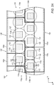
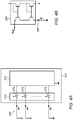
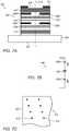
- FIG 2A schematically depicts a side of a writing module 100 that faces the imaging surface.
- Writing module 100 may exemplify some embodiments of writing modules 40 and 82 depicted in Figures 1A-1C .
- Writing module 100 comprises several integrated electronic modules 110 (designated specifically 110a , 110b etc .), each constructed as an electronic die or chip and comprising an array 112 of light sources 120.
- Integrated electronic modules 110 are mounted, directly or indirectly, on a heatsink or a cooler (not depicted in this figure), configured to remove excess heat from the integrated electronic modules 110 during operation, as is explained in detail further below.
- the surface of integrated electronic modules 110 that faces the heatsink is termed herein the rear surface (or rear side) of the module, whereas the other surface (which is viewed in the figure) is identified herein as the front side or the light-emitting side.
- Integrated electronic modules 110 are VCSEL dies, as detailed further below.
- Each array 112 comprises rows 114 and columns 116 , and is arranged to be skewed so that the rows 114 are parallel to the Y direction and the columns 116 are tilted at an angle ⁇ relative to the X direction.
- the angle ⁇ is determined so that the locations of the light sources 120 along the Y direction are equally spaced, namely the projection on the Y axis of the locations of the light sources 120 in each array form an equally spaced grid.
- arrays 112 are similar to one another, each having an equal number, five, of rows and columns.
- integrated electronic modules 110 may comprise additional light sources (not depicted here) to the light sources in the arrays 112. Such additional light sources may be employed as redundancy, or spare, to bridge gaps in the grid of light spots along the Y direction due to, e.g., failed light sources within the array, or due to e.g., minor dislocations ( e . g ., resulting from misplacement) of one integrated electronic module 110 relative to another during assembly.
- the arrays 112 are arranged in the illustrative figure along two lines 118a and 118b, the lines extending parallel to the Y direction, and being spaced apart from one another along the X direction.
- the arrays are arranged along the lines 118a and 118b in a staggered arrangement so that neighboring arrays along the Y direction are positioned on different lines alternatingly.
- the arrays neighboring (along the Y direction) an array on line 118a are located on line 118b
- arrays neighboring an array on line 118b are on line 118a .
- Writing module 100 further comprises an optical system 128 configured to focus the light beams of light sources 120 onto an imaging surface (e . g ., imaging surface 22 or 88 as respectively exemplified in Figures 1A and 1C - the imaging surface is not depicted in Figure 2A ).
- optical system 128 is configured to image light sources 120 onto imaging surface 22.
- optical system 128 comprises lenses 130 each lens 130 being associated with one array 112 of light sources.
- An optical system comprising micro-lenses wherein each lens is associated with one light source, and preferably manufactured together with the light source, is also contemplated.
- an optical system may comprise optics (e . g ., lenses), so that a single lens may image a group of VCSEL dies onto the imaging surface, and the adjacent lenses are lined up in the Y direction.
- the lenses 130 comprise Gradient Index (GRIN) lenses.
- GRIN lenses are preferred compared to spherical lenses, because GRIN lenses, which are constructed as elongated rods 132 extending along the Z axis, may be self-aligned during assembly as is described herein below.
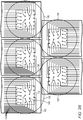
- a bottom view of the rods 132 is presented.
- rods 132 are of identical diameter and are arranged (in the X-Y plane) in a close-packed arrangement in two rods lines 134a and 134b , corresponding to lines 118a and 118b , respectively. In such an arrangement, the rods 132 are self-aligned (in the Z direction) parallel to one another, hence the light beams focused by different rods are also aligned substantially parallel to one another.
- arrays 112 are spaced apart along the lines 118a and 118b , in 1-to-1 correspondence to the positions of rods 132 along the rods lines 134a and 134b , respectively. In other words, the arrays are located so that the light beams produced by each array may be focused by one GRIN rod 132 (onto imaging surface 22 ). If arrays 112 are identical to one another, then the distance between corresponding points of neighboring arrays along any of the lines ( 118a or 118b ) is equal to the diameter of rods 132.
- the magnification of optical system 128 may be +1 or -1 or any other number, preferably having an absolute value smaller than 2, still preferably being relatively close to 1. If the magnification is +1 or -1, then the light beams of each array generate an array of spots on imaging surface 22 , substantially identical with the array 112. Thus, when the magnification of optical system 128 is +1 or -1, the arrays 112 are spaced apart along the lines 118a and 118b , so that the locations along the Y direction of the light sources of two neighboring arrays are equally spaced.
- the distance, along the Y direction is equal to the distance between two locations along the Y direction of neighboring light sources in a same array.
- the absolute value of the magnification of optical system 128 may be different from 1, namely either higher or lower than 1, and consequently an imaged array of light spots on the imaging surface is larger or smaller than the corresponding array 112 , respectively.
- the magnification is larger than 1
- each array's image is magnified through optical system 128 , hence to obtain on the imaging surface an equally-spaced grid of light spots along the Y direction, neighboring arrays should have a gap between their closest light sources, which is larger than the gap along the Y direction between neighboring light sources on a same array.
- the spacing along the Y direction of light sources on a specific die in such a case needs to be smaller than the intended spacing between the imaged light spots (which relates to the address resolution of the printing system). And vice versa - if the absolute value of the magnification is smaller than 1, then each array's image is shrunk through optical system 128 , hence to obtain an equally-spaced grid of light spots along the Y direction, neighboring arrays should partially overlap along the Y direction.
- a magnification of +1 by the optical system 128 is preferred in some embodiments. If the magnification is positive, a dislocation of a lens relative to the related array may be compensated, at least partially, by the lens, in that the dislocation of the resulting light spots on imaging surface 22 is diminished. In comparison, in a case of a negative magnification, such a misalignment of a lens may be magnified so that the dislocation of the resulting light spots on imaging surface 22 is enhanced.
- Embodiments of writing module 100 may comprise integrated electronic modules 110 in various shapes and sizes as is demonstrated in Figure 2A .
- integrated electronic modules 110a and 110b each include a single array 112.
- Integrated electronic module 110c is arranged as a rectangle including two arrays 112.
- Other embodiments may include rectangle integrated electronic modules 110 having more than two arrays arranged in a line.
- Integrated electronic module 110d comprises four arrays 112 , two of which are arranged on line 118a and two on line 118b. It is noted that including on a single die of integrated electronic modules 110 arrays from both lines 118a and 118b may necessitate that the border line of the die is not rectangular nor is it quadrilateral, which implies more complicated cutting technique (compared to a rectangular-shaped die).
- a relatively large integrated electronic module 110 including several arrays 112 , contributes to decreasing mismatch between locations of neighboring arrays 112 in a single writing module 100 during assembly, and hence contributes to eventual higher writing quality in the printing system. Further, such a relatively large integrated electronic module 110 allows for a more compact configuration of the arrays, by minimizing dead space which is generally associated with the edge of the die. On the other hand, large integrated electronic modules 110 tend to be very brittle.
- an integrated electronic module 110 may include one or two or even more arrays 112 , but the overall dimensions thereof may preferably be limited to less than a few centimeters and according to some embodiments even less than one centimeter.
- integrated electronic module 110 may result in reduced yield of manufacturing, as a single die that includes several arrays includes more light sources, thus increasing the likelihood of a failed light source on a specific die.
- writing module 100 may typically comprise several integrated electronic modules 110 , and possibly tens or even hundreds of integrated electronic modules 110 assembled side by side.
- integrated electronic modules 110 may comprise electric contacts on the front (light-emitting) surface thereof, thereby enabling feeding electric signals to the light sources via the front side and thereby enabling mounting the integrated electronic modules 110 directly on an electrically isolating surface of the heatsink, thus enabling efficient heat removal from the module during operation.
- the heatsink can be passive or active, depending on the amount of heat one needs to remove under particular operating conditions. It is noted that electric contacts of the integrated circuit on the front side may be positioned according to common manufacturing techniques on the periphery of the die, thus necessitating a net of conductors on the die that electrically and exclusively connect each light source with at least one contact.
- integrated electronic module 110 may be mounted on a sub-mount using contacts on the back side of the die for electric connections.
- Such contacts - e . g ., employing a Ball Grid Array (BGA) or another solder bumps technology - may each be positioned on the back side directly opposite the location of one light source, thus withdrawing the need for a net of conductors across integrated electronic module 110 itself.
- BGA Ball Grid Array
- handling and assembly (mounting) of integrated electronic module 110 using a sub-mount as described herein may be a more efficient method compared to direct mounting on the heatsink as described above; however, heat removal from the integrated electronic module 110 through the sub-mount towards the heatsink may be inferior.
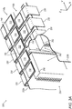
- Writing module 100 comprises sub-mounts 140 ( e . g ., 140a, 140b etc .) for mounting integrated electronic modules 110 thereon as explained above.
- sub-mount 140 may comprise a substrate made from a highly thermally conducting, electrically insulating material.
- the substrate may be selected from the group comprising aluminum nitride (A1N), having thermal conductivity of 170W/(m ⁇ °K) and thermal expansion coefficient of 4.6•10 -6 ⁇ °C -1 ; beryllium oxide (BeO), having thermal conductivity of 270W/(m ⁇ °K) and thermal expansion coefficient of 9•10 -6 ⁇ °C -1 ; and CVD diamond, having thermal conductivity of 1000W/(m ⁇ °K) and thermal expansion coefficient of 1•10 -6 ⁇ °C -1 .
- A1N aluminum nitride
- BeO beryllium oxide
- CVD diamond having thermal conductivity of 1000W/(m ⁇ °K) and thermal expansion coefficient of 1•10 -6 ⁇ °C -1 .
- CVD diamond demonstrates the highest thermal conductivity, however the thermal expansion coefficient is the most distant, within the group of materials listed above, from the thermal expansion coefficient of GaAs, 5.73•10 -6 ⁇ °C -1 (GaAs being the typical substrate in VCSEL dies). In this group aluminum nitride has the closest thermal expansion coefficient to that of GaAs, but the lowest thermal conductivity.
- FIG. 2A schematically depicts several illustrative examples of sub-mounts having various sizes and shapes.
- Sub-mounts 140a and 140b are similar to one another, each being dimensioned and configured to be connected to single arrays 112.
- integrated electronic module 110c comprising two arrays 112
- Sub-mount 140c is electrically connected to sub-mounts 140a and 140b , each array being connected to one of the two sub-mounts, respectively.
- Sub-mount 140c is dimensioned and configured to be connected to two arrays 112 , positioned side by side along one of the lines 118a or 118b.
- integrated electronic module 110a and integrated electronic module 110b are both assembled onto sub-mount 140c .
- Sub-mount 140d is dimensioned and configured to be connected to four arrays 112 , positioned as a neighboring quartet on both lines 118a and 118b.
- integrated electronic module 110d (comprising four arrays 112 ) is assembled onto sub-mount 140d .
- Sub-mounts according to the description hereinabove may be provided within a range of thicknesses, e . g ., between about 100 ⁇ m and about 1mm. There are therefore various and even conflicting considerations that may apply to the selection of size and thickness of sub-mounts 140.
- a relatively large sub-mount 140 allowing the assembly of several arrays 112 thereto, contributes to decreasing mismatch between locations of neighboring arrays 112 in a single writing module 100 during assembly, and hence contributes to eventual higher writing quality in the printing system. Further, such a relatively large sub-mount 140 allows for a more compact configuration of the arrays, by minimizing dead space which is generally associated with the edge of the sub-mount.
- heat removal may be a dominant consideration, favoring a thin sub-mount and thereby allowing for more efficient heat removal from the integrated electronic module 110 through the sub-mount towards the heatsink. Since a thin sub-mount tends to be very brittle, small sub-mounts, providing connections to only a small number of arrays 112 - e . g ., four arrays or two arrays or even only one array - may be preferred. Also, as a higher number of arrays are assembled onto a single (larger) sub-mount, the higher also is the likelihood of a failure (either during assembly or later during machine operation) necessitating replacement of a large fraction of the light sources in the writing module.
- the surface of the metallic cooler can deposit on the surface of the metallic cooler a thin layer (e . g ., of a few microns, typically less than 2 ⁇ m) of electrically insulating and thermally conducting material.
- a thin layer e . g ., of a few microns, typically less than 2 ⁇ m
- the surface of the cooler can be coated ( e . g ., by sputtering) with a thin layer of Aluminum Nitride, upon which electrical conductors are subsequently applied to individually convey the driving signals to each light emitting element.
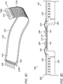
- Electrical connections to the arrays may typically be provided by metallized lines disposed on the surface of the sub-mount, typically connecting a set of contacts (e . g ., arranged in a connector or array of contacts 138 ) and an array of pads on the sub-mount configured to solder to the solder bumps of the integrated electronic module 110 (such lines being explicitly illustrated in Figure 2B ).
- a set of contacts e . g ., arranged in a connector or array of contacts 138
- an array of pads on the sub-mount configured to solder to the solder bumps of the integrated electronic module 110 (such lines being explicitly illustrated in Figure 2B ).
- the lateral density of conducting lines on the sub-mount along the Y direction corresponds at least roughly to the density of light sources along the Y direction, divided by 2.
- the following is a non-limiting numerical example illustrating the tight constraints associated with the current conducting lines of the sub-mount.
- the lateral spacing of light sources along the Y direction is about 50 ⁇ m, hence, about 20 light sources are distributed along each 1mm along the Y direction and about 20 conducting lines may be provided along each such 1mm for connecting each light source.
- the conducting lines to arrays 112 on line 118a and to the arrays 112 on line 118b may be directed from opposite directions (namely from top and bottom of Figure 2A ), hence a total width of each line together with an adjacent spacing to a next conducting line may roughly be of about 100 ⁇ m.
- the conducting line thickness is limited both in absolute value and in aspect ratio.
- the absolute thickness may be limited to several tens of ⁇ m ( e . g ., 10 or 20 or even 30 ⁇ m) whereas the aspect ratio of the cross section of the conducting line may be limited to 1:1 or even less (hence the thickness of a 20 ⁇ m wide line, for example, may not be larger than 20 ⁇ m, and may typically be even less).
- 500mAmps of current generate in the same configuration a temperature rise of 170°C and a power loss of about 30mW on a 3mm-length conductor. It should be understood that if the spacing of the light sources along the Y direction is smaller than 50 ⁇ m (possibly allowing a higher address resolution of the printing system) then the conducting line width should preferably be smaller, resulting in yet even more tight constraints on the allowed current through the conductor.
- Figure 2B schematically depicts a detailed view of a portion of sub-mount 140 , showing an array of pads 142 corresponding to array 112 with 5 rows and 5 columns of lights sources (only the outline of array 112 is depicted in the figure). Each pad 142 is electrically connected to a conducting line 144. It should be noted that various and even conflicting considerations may apply to the physical dimension of array 112 and to the total number of light sources in each array. It is noted in this regard that array 112 preferably roughly forms a quadrilateral shape with four substantially equal sides.
- the optical quality of the lens 130 is typically lower towards the lens' periphery, namely the imaged spot of a light source near the periphery of the array (being away from the lens center and close to the lens periphery) is typically bigger than the spot of a center light source.
- a square array allows producing more uniform imaged light spots, compared to a rectangular array.
- a small array of light sources is difficult to implement for at least two reasons.
- a small number of light sources in a column implies a small distance between two neighboring light sources in a same row, and overall small dimensions of the die. For example, in an array of 2x2 wherein the distance between two adjacent projections on the Y axis of the locations of the light sources ( i . e .
- the distance between two adjacent light spots in case the magnification is ⁇ 1) is about 50 ⁇ m, the distance between two neighboring light sources in a row is twice as large, namely about 100 ⁇ m, which may be difficult to manufacture.
- the overall dimension of the die in this case may be roughly 0.3-0.4mm, which may be, in some embodiments, more costly to manufacture due to a large number of dies, and difficult to handle and to assemble.
- the distance between two neighboring light sources in a row can be about 250 ⁇ m and the overall dimension (side length) of the die can be about 1.5mm.
- a second difficulty associated with small arrays is the resulting small diameter of the lenses 130.
- the lens diameter may be about 0.7mm which may be difficult to handle and to align with neighboring light sources arrays.
- the lens diameter may be about 5mm, lending itself for much simpler handling and alignment.
- an array of a large number of light sources may also be difficult to implement.
- the physical dimension of the array should preferably be larger. Firstly, assuming the distance between neighboring light sources in a column remains constant, the overall dimension of the array's size is enlarged, as more light sources are included in the array. Secondly, as more light sources are included in the array, the distance between neighboring light sources in a column should preferably increase, to allow more conducting lines to extend in between neighboring light sources on the array's periphery and reach light sources in the internal portions of the array.
- array's dimensions namely array's side length for an approximately square-shaped array
- a large array may be difficult to implement for at least two reasons: first, a large array implies a large die that might be extremely brittle due to size. For example, a 50x50 light sources array with the same Y -axis grid spacing specified above of 50 ⁇ m, may have a side length of about 40-60mm. As explained above regarding the integrated electronic module 110 overall dimensions, a corresponding die having a side length of about 4-6cm might be too big to manufacture, too big to handle and too big to assemble reliably. Further, a large array necessarily implies a lower yield during manufacturing (as any single defected light source or a local defect in the wafer may disqualify the whole die).
- a second difficulty in implementing large arrays in writing module 100 is associated with the resulting large distribution of locations of light sources along the X axis.
- a large distribution of locations of light sources along the X axis implies a large distribution of distances between the points of irradiation of the imaging surface, and the nip, resulting, in turn, in a large spread of time gaps between the event of modifying the polymer on the imaging surface by the light sources and the event of impression.
- the die of integrated electronic module 110 may be (that is, have a side length) larger than about 0.5mm and smaller than about 25mm, being preferably between 0.8mm and 20mm, still preferably between 1mm and 10mm and more preferably between 1mm and 5mm.
- array 112 of light sources may, according to some embodiments, be larger than about 2x2 and smaller than about 50x50, being preferably between about 3x3 and about 30x30, more preferably between about 5x5 and about 20x20. It is emphasized that according to some embodiments, specifically embodiments requiring higher or lower printing resolution compared to the printing resolution discussed explicitly here, larger or smaller arrays may be contemplated.
- the writing module further comprises an electronic driver circuitry, electrically associated with the light sources and configured to individually activate and deactivate the light sources.
- Figures 3A and 3B depict schematically an embodiment of a writing module 200 as can be assembled, in perspective view and in side view, respectively.
- Writing module 200 can comprise writing module 100 as described above, attached by its rear side to a bottom face 212 of a heatsink 210 (depicted explicitly in Figure 3B ). For the sake of clarity, the lenses are not depicted in these Figures and the heatsink is not shown in Figure 3A .
- Writing module 200 further comprises electronic circuitry 220 deployed from two sides of writing module 100.
- electronic circuitry 220 is deployed on at least two electronic boards 222a and 222b ( e . g ., Printed Circuit Boards, PCB) attached to two side faces 214 and 216 , respectively, of the heatsink.
- electronic boards 222a and 222b e . g ., Printed Circuit Boards, PCB
- Flex circuit 230 comprises a multitude of conducting lines, electrically isolated from one another and mechanically associated together to form a flexible, preferably flat assemblage of conductors. Flex circuit 230 is thus configured to provide a mechanically-flexible and massively-parallel electrical conduction for conducting the driving signals to the individually controlled light sources. According to some embodiments, flex circuit 230 comprises also a common conductor line, configured to commonly conduct the return current from all or at least some of the light sources in the integrated electronic module 110. The common line may have a larger cross-section than a single signal conducting line to carry the return current of at least some or all of the light sources.
- a flex circuit 230 may comprise a Flexible Flat Cable (FFC) comprising a multitude of parallel flat conducting lines disposed on a thin and flexible dielectric layer or laminated between two thin and flexible dielectric layers.
- a flex circuit 230 may comprise a Flexible Printed Circuit (FPC), typically manufactured by photolithography, as is well known in the art.
- FPC Flexible Printed Circuit
- a typical FPC may comprise photolithographed flat metallic conductors typically made of copper or another well-conducting metal, bonded or deposited onto a thin and flexible dielectric substrate, e . g ., made of polyimides or polyesters, such as Polyethylene Naphthalate (PEN) or Polyethylene Terephthalate (PET).
- PEN Polyethylene Naphthalate
- PET Polyethylene Terephthalate
- one flex circuit 230 is associated with one sub-mount 140 , however such a correspondence is not mandatory.
- sub-mount 140 has assembled thereon one integrated electronic module 110 comprising a single array 112 of light sources, and is electrically associated with a single flex circuit 230.
- Double flex circuit 232 comprises a double-sided FFC, comprising a dielectric layer 234 extending between a first end 236a and a second end 236b.
- Double flex circuit 232 further comprises multiple conducting lines 238 disposed on a first surface of the dielectric layer, being configured to conduct the driving signals to the individually controlled light sources.
- Multiple conducting lines 238 extend from a first array of pads 242 on the first end 236a to a second array of pads (not shown here) on the second end 236b.
- the first array of pads 242 is configured to connect ( e .
- each conducting line 238 electrically connects a single pad in the first array to a single pad in the second array.
- Double flex circuit 232 further comprises a single conducting line 240 disposed on the second surface of the dielectric layer and configured to commonly conduct the return current from the light sources, thereby functioning as a common line.
- the common line 240 extends from first end 236a to second end 236b , and electrically connects a pad 244 on the first surface of the dielectric layer to one or more pads 246 on the second end 236b.
- Pad 244 may be electrically connected to the common line 240 , for example, through via-holes (not depicted here) - from the first surface to the second surface.
- Pad 244 may be configured to connect ( e . g ., by soldering) to a corresponding common pad on the PCB carrying the electronic circuitry.
- One or more wires 248 may be used to connect the one or more pads 246 on the second end 236b , to a common contact of the integrated electronic module 110 (not shown here), e.g., using wire bonding technique.
- the common contact is conveniently disposed on the surface of the die opposite to the surface of the individual control contacts to the VCSELs.
- the common contact may face the opposite direction, being disposed on the front side of the die, thereby being accessible for such wire bonding.
- the common line may be electrically connected to a pad (not shown here) on the first surface of double flex circuit 232 , which is configured, in turn, to be soldered to the sub-mount (or to the light sources die) thus eliminating the need for wire bonding.
- the wires 248 may be relatively thin, having a diameter smaller than e .
- wires may connect the common line 240 to the common contact on integrated electronic module 110 , so as to maintain mechanically-flexible, yet good conduction path, thereby providing a relatively small voltage drop on such connection during operation.
- wire-bonding technique may be used, according to some embodiments, to connect the electronic circuitry on the boards 222 and the sub-mount (or the integrated electronic module 110 ) using a mechanically flexible connection.
- a multi-layer flex circuit may be used for connecting the electronic circuitry 220 and the light sources. It is alternatively possible for the common contact and the signals contacts to be disposed on the same side of the light-sources die, thus allowing connection to the die from a single side thereof.
- flex circuits 230 for electrical connection between the sub-mount 140 and the boards 222 allows a relatively simple, massively parallel, electrical connection over the "corners" between bottom face 212 and the side faces 214 and 216 of heatsink 210. Also, flex circuits 230 allow a relatively simple connection between two different substrates of the module - namely the sub-mount and the electronic boards - as integrated electronic module 110 may, preferably, not be assembled onto a board such as a PCB, and electronic circuitry 220 may, preferably, not be installed directly on sub-mount 140.
- Figure 3D schematically depicts an embodiment of a writing module 250 wherein the sub-mount 140 and the electronic boards 222 are assembled onto a heatsink 252 aligning along a same plane.
- the sub-mount 140 and the electronic boards 222 are connected via a massively-parallel flexible connection, e . g ., double flex circuits 232. It is noted that, even in the configuration of writing module 250 , a rigid connection between the electronic boards 222 and the sub-mount (or with the die of integrated electronic module 110 ), instead of double flex circuits 232 (or, for that matter, any type of flex circuit), might be less than optimal. First, inevitable mechanical misalignment and tolerances of the mutual positions of the sub-mount (or the die) and the boards of the electronic circuitry may decrease or jeopardize the reliability or durability of such a rigid connection. Moreover, due to different temperatures and different temperature expansion coefficients of the sub-mounts 140 and the boards 222 , a rigid connection therebetween might affect detrimentally the mechanical integrity of one, or both, during operation.
- the relatively high density of conductors on flex circuit 230 poses an upper limit or at least a barrier on the available conducting cross-section of each conducting line, thereby implying an upper limit or at least a barrier on the current that may reliably be conducted in such a conducting line.
- the following is a non-limiting numerical example illustrating the tight constraints associated with the conducting lines of flex circuit 230.
- the example employs some common assumptions as detailed above regarding the current conducting lines on the sub-mount 140. According to the example, the lateral spacing of light sources along the Y direction is of about 50 ⁇ m, hence a total width of each conducting line together with an adjacent spacing to a next conducting line may roughly be about 100 ⁇ m.
- a current of 300mAmps generates a temperature rise of about 60°C in the conductor (in ambient air, and independent of the conductor length). It is noted in this regard that according to presently available technology, the thickness of a conducting line having a width of several tens of micrometers, on a flex circuit, may not typically exceed 10 ⁇ m, and may even be limited to yet a smaller value.
- 500mAmps of current generate in the same configuration a temperature rise of 170°C, a power loss of about 300mW, and a voltage drop of about 0.6V on a 30mm-length conductor.
- a 300mW power loss is equivalent, namely roughly equal, to a required light power from each light source according to some embodiments.
- a 500mA of driving current through the conducting lines of the present example may result in significant efficiency loss and therefore a tremendous heat removal problem.
- a voltage drop of a few tenths of a volt on the conducting lines e . g ., about 0.6V as in the example above
- the conducting line width should preferably be lower, resulting in yet even more tight constraints on the allowed current through the conductor.
- electronic circuitry 220 may comprise a current driving stage configured as a voltage source to light source 120. Additionally, or alternatively, electronic circuitry 220 may comprise a current driving stage configured as a current source to light source 120. It is noted that two VCSELs may differ in electrical resistance when activated and driven by a same current or by a same voltage. Moreover, the electrical resistances of two different conducting lines between two VCSELs and the associated driving stages, may be different from one another. Hence, a same current driven into two VCSELs may require a different voltage at the output port of the associated driving stages. It is further noted that different individual VCSELs may require different levels of current, to output a same level of light power.
- an individual calibration function may be established for each VCSEL, the function defining the current (or voltage, in some embodiments) that should be provided at the output of the associated driving stage, to produce a pre-determined light power by a particular VCSEL. It should be understood that due to temporal changes that may occur to the VCSEL and/or to the conducting lines thereto, the calibration function may preferably be updated periodically or intermittently, by employing a calibration process.
- FIG 4A schematically depicts a block diagram of an embodiment of a driving module 270 , configured to electrically and individually connect to a multitude of light sources 280 comprising VCSELs, and thereby drive suitable currents to the light sources (previously schematically illustrated by dots 120 in Figure 2A ).
- Driving module 270 comprises a control module 272 , configured to receive commands to activate or deactivate any single light source or any combination of light sources 280.
- Control module 272 is further configured to receive calibration data, associating, for each of light sources 280 , a driving current (or an input voltage, according to some embodiments) with a light output power.
- Driving module 270 further comprises a driving stage module 274 , comprising a multitude of driving stages 276.
- Each driving stage 276 is configured to receive from control module 272 a signal indicating a current (or a voltage) that should be driven to an associated light source 280. Driving stage 276 is further configured to output the required current (or, in some embodiments, the required voltage), so as to yield a desired light output from the associated light source.
- Figure 4B depicts schematically a particular implementation of a current driving stage 284 configured to drive current suitable for activating some embodiments of a GaAs VCSEL light source 286.
- Current driving stage 284 may be configured to switch VCSEL light source 286 between two levels of output light power, namely between an ON state and an OFF state (equivalent to zero-output power), generally requiring different current levels to be supplied to the different VCSELs (at least in the ON state) to produce a same output light power, as explained above.
- current driving stage 284 may be configured to activate VCSEL light source 286 at more than two levels of output light power, namely to activate VCSEL light source 286 to produce an intermediate power of light output, in addition to producing a maximum power output level and a zero-power output level.
- current driving stage 284 may activate VCSEL light source 286 at more than four different levels of output power, or more than six or more than ten, or even more than fifteen different levels of output light power. The use of several calibrated levels of output light power is advantageous in a printing system, for enabling fine-tuning of printed line widths and fine tuning of printed regions' border lines.
- various calibrated levels of output light power may enable, respectively, printing of various dot sizes within a pixel or within a pre-defined area comprising several pixels, thereby enabling controlling the grey level of a printed region.
- the use of several calibrated levels of output light power may enable compensating for a failed light source by using neighboring light sources, as exemplified below in Figures 5A - 5D .
- driving stage 276 or current driving stage 284 is configured to drive into a VCSEL light source a current greater than about 50mA, or greater than about 100mA, or greater than about 150mA. In some embodiments, driving stage 276 or current driving stage 284 is configured to drive into a VCSEL light source a current of less than about 200mA. In some embodiments, driving stage 276 or current driving stage 284 is configured to supply to a VCSEL light source a switching voltage which is determined according to the number of semiconductor junctions connected in series in the light source.
- driving stage 276 or current driving stage 284 may be configured to supply a maximal driving voltage between 3V and 8V.
- driving stage 276 or current driving stage 284 may be configured to supply a maximal driving voltage between 5V and 15V.
- Figures 5A - 5D illustrate schematically power profiles of light spots generated by a group of neighboring light sources, and the resulting combined power profile delivered by the group. It is emphasized that, for sake of explanation, the figures relate to a simplistic, one-dimensional example of idealised light spots arranged along a line, whereas a more realistic and quantitative analysis should take into account the two-dimensional nature of the light spots on the imaging surface during printing system operation.
- Figure 5A illustrates spot profiles 502a ⁇ 502g of the power of seven light spots arranged along the Y axis.
- the spot profiles are assumed to have a Gaussian shape of arbitrarily-selected maximal intensity of about 1 and half width at half maximum of about 1.
- a combined profile 504 represents the total power, namely the sum of the powers of the spot profiles, along the Y axis.
- Figure 5B illustrates spot profiles 522a ⁇ 522d and 522f ⁇ 522g , of the power of 6 light spots arranged along the Y axis as in the example of Figure 5A .
- a spot profile 522e is absent, representing an inoperative seventh light source.
- a similar outcome might have been obtained, were the inoperative light source merely defective so that its reduced spot profile does not suffice to allow reaching the threshold, even in combination with neighboring profiles of operative light sources.
- the power of light sources neighboring to the defected light source may be increased, as is demonstrated in Figure 5C .
- spot profiles 542d and 542f (on both sides of an absent spot profile 542e ) are doubled in power, reaching a maximal intensity of 2.
- increasing the output light power of a light source beyond a nominally standard level may be used to compensate for a neighboring light source which is inoperative or defective.
- fine tuning the location of the end of the print line namely fine-tuning the location where the combined profile 544 crosses the threshold h , may be achieved by fine-tuning the intensity of spot profile 544g , as is demonstrated in Figure 5D .
- Figure 5D illustrates spot profiles 562a ⁇ 562g whereas spot profiles 562a - 562f have a nominally standard intensity of 1, and spot profile 562g has half the intensity, namely a maximal intensity of 0.5.
- the driving stages of the electronic circuitry are preferably positioned close to the light sources.
- driving stages 276 are preferably positioned close to light sources 280 in Figure 4A . Minimizing the length of conducting lines between the driving stages and the light sources, results in minimizing power loss and heat dissipation on such conducting lines, minimizing signal distortions due to parasitic inductance and mutual capacitance of the conducting lines, and maximizing switching bandwidth of the driving module 270.
- the driving stages (such as driving stages 276 of Figure 4A , for example) for driving current to the multitude of light sources in arrays 112 , are arranged in electronic chips 290 (depicted here within conventional electronic packages 292 ), deployed on boards 222.
- each electronic chip 290 is electrically associated with the light sources in two neighboring arrays 112 along one of the lines 118a or 118b.
- each array 112 comprises five rows and five columns of light sources at a grid spacing of 50 ⁇ m along the Y axis
- each array comprises twenty-five light sources, capable of radiating along a continuous segment of about a 1.25mm length along the Y direction.
- a single electronic chip is electrically associated with fifty individual light sources, spanning together two such non-consecutive segments along the Y axis.
- two electronic chips 290 positioned oppositely to one another on the two boards 222a and 222b , are electrically associated with a hundred light sources, spanning together a consecutive segment of about 5mm length along the Y direction.
- a row of electronic chips 290 , packaged in electronic packages 292 , each having a width (as measured along the Y direction) of about 4.5mm may be installed side by side with a 0.5mm gap in between, on each of the boards 222a and 222b.
- Each electronic package may further have a length (measured along the Z direction) of about 1cm or 2cm or even 3cm, and a consequent area of about 0.5cm 2 or 1 cm 2 or even 1.5cm 2 , such area being configured to allow heat dissipation from the electronic chip into the heatsink 210.
- electronic chip 290 may be configured to switch ("on” and “off only) 50 individual GaAs VCSELs, wherein the maximal ("on") current is about 50mA, and the voltage drop on each driving stage during "on" time is about 2V.
- the electronic chip may consume a maximum power of about 5W and may span an area of about 70mm 2 .
- modifying a polymer for accomplishing the print process typically requires a pre-determined energy density defined as the energy per unit length of the print format.
- the power density required for the process - being derived from the energy density - is linearly dependent on the printing speed.
- the density of VCSEL light sources i.e. the number of sources per unit area
- the grid spacing of the VCSEL light sources along the Y direction may be smaller than 50 ⁇ m, being for example 40 ⁇ m or 30 ⁇ m or even 20 ⁇ m.
- Each electronic chip 290 is then preferably configured to switch a correspondingly higher number of VCESLs light sources, e.g., about 60, or about 80 or about 120 individual VCESLs light sources.
- the area of each chip may correspondingly be larger, as more switches are integrated on a single chip, and heat dissipation on the chip during operation may be larger too.
- the driving stage is configured to drive current at several non-zero current levels to obtain light radiation at several non-zero levels (as exemplified e .
- the average heat dissipation on the chip is larger, and the area of the chip should also preferably be higher (compared to an embodiment configured for only on-off switching).
- a layout of electronic circuitry 220 may be realized by many embodiments other than those explicitly detailed above.
- electronic chips such as 290 may be configured to be associated to a different number of arrays 112 , in particular to a greater number than 2 arrays, for example to 3 or 4 arrays or more, thereby reducing dead space in boards 222 due to gaps between packages 292 , hence allowing a greater chip area for heat removal.
- Figures 6A - 6E depict some embodiments of a light source 300 comprising a cluster 310 of VCSELs disposed adjacent to one another and electrically connected to one another in series.
- Figure 6A depicts a portion of an array 312 of light sources 300 , comprising rows 314 and columns 316 , skewed so that the rows 314 are parallel to the Y direction whereas the columns 316 are tilted at an angle ⁇ relative to theXdirection, as is described above regarding array 112.
- a distance between neighboring light sources is marked D (denoted here along column 316 ).
- a grid spacing along the Y direction - that is to say, the distance between neighboring projections on the Y axis of the locations of the light sources - is denoted r.
- r determines the address resolution, being related to (and in some embodiments being equal to) the printing resolution of the printing system.
- the distance D in some embodiments, is determined by various manufacturing considerations, some being explained above.
- the distance between neighboring light sources along row 314 is roughly equal or exactly equal to the distance between neighboring light sources along column 316.
- Figure 6B schematically depicts five different embodiments of light source 300 , comprising clusters 310a , 310b , ... 310e , of three, four, five, six, and seven VCSELs 320 , respectively.
- VCSELs 320 in each cluster are configured and operable to radiate together, and are spatially arranged and optically configured to produce a single light spot on the imaging surface of the printing system when activated, as is further explained below.
- a diameter (or dimension) of light source 300 is denoted d and is determined by a diameter of a circle 324 encompassing the cluster 310 of VCSELs 320 of the single light source.
- d may be smaller or larger than r and is typically roughly equal to r, whereas D is typically larger than d .
- Figure 6C depicts schematically a side view of light beams 330 generated by two clusters 310 of VCSELs 320.
- the divergence angle of light beams produced by VCSELs according to currently available technologies is typically in the range of 5 - 25 degrees (half angle).
- the distance s between a plane 332 of the active region of the VCSELs and a plane 334 wherein adjacent light beams merge (coincide) is about 1.5 to 5 times the distance between neighboring VCSELs in a cluster (here s is measured along the optical axis of the VCSELs, coinciding with the Z axis). If the distance between neighboring VCSELs is, for example, 10 ⁇ m, then the distance between the planes 332 and 334 may be about 15 ⁇ 50 ⁇ m.
- Cluster 310 may produce a single light spot on the imaging surface using the optical system (not shown here) of the printing system.
- the optical system - such as, e.g., optical system 128 in Figure 2A - may be configured to image onto the imaging surface the plane 334 or another plane which is distal from the plane 332 of light sources.
- the optical system may be tuned to image light sources 300 onto the imaging surface with some defocus - typically a slight defocus, thereby blurring the image of the light sources on the imaging surface, and thereby forming from the light beams from each cluster 310 a single light spot.
- inevitable blur of the optical system resulting for example from aberrations or diffraction, may cause imaging the cluster on the imaging surface as a single spot, even without defocus.
- the arrangement and orientation of VCSELs 320 in cluster 310 is preferably determined relative to the X direction so that traces of the activated VCSELs (in a single cluster) overlap and merge into a single light spot on the imaging surface (not depicted here) during the duration of a single pixel formation.
- each light beam emerging from a VCSEL traces a short line on the imaging surface due to the continuous motion of the imaging surface.
- each VCSEL leaves on the imaging surface a trace, the length of which is determined by the pixel duration and the imaging surface's velocity, and the width of which is determined by the diameter of the light beam on the imaging surface.
- the partial overlap and merger of the light beams of each cluster 310 together with the motion of the imaging surface during the pixel duration, hence produce a single light spot from the cluster of VCSELs.
- Figure 6D schematically depicts an equivalent electrical circuit 340 of a cluster of VCSELs electrically connected in series.
- Circuit 340 comprises, as an illustrative non-limiting example, three VCSELs 320 represented as light-emitting diodes 342a , 342b and 342c , respectively, connected in series, each having an active region comprising one junction.
- such cluster of three VCSELs may output roughly three times the light output power of a single VCSEL, at the same operating current.
- a light source 300 comprising a cluster 310 of VCSELs may be configured ( e . g ., the number of VCSELs in the cluster be determined) in a process according to the following sequence of steps: first, a desired operating current for the light source may be selected. Such a desired operating current may be selected so as to determine a relatively highly-efficient working point for a single VCSEL in the cluster, and also while considering limitations of current-conducting lines and switching frequency of the circuitry associated with the VCSEL, as explained and detailed herein above. Then, the light output power of a single VCSEL at the selected working point may be estimated using the light output power equation (1) given above. Then, the desired light output power from a single light source may be divided by the light output power of the single VCSEL, to determine the required number of VCSELs in the cluster.
- FIG. 6E schematically depicts a cross-section view of two VCSELs, 320a and 320b , respectively, connected in series in a two-VCSELs cluster 346 (the suffixes 'a' and 'b' to numerals of this figure representing elements in the respective VCSELs 320a and 320b ).
- the VCSELs are constructed above a substrate 348 , being isolated therefrom by a thin isolating layer 350.
- Each VCSEL comprises a bottom Bragg reflector 352 , a partially-reflecting top Bragg reflector 356 above bottom Bragg reflector 352 , and an active region 354 between the bottom and top Bragg reflectors.
- the VCSELs typically further comprise an oxidized layer having a conducting aperture (which is not explicitly depicted here) for confining the current and thereby defining the beam width.
- a positive electrical contact 360 may generally reside on top of the substrate 350 , being electrically separated therefrom by the insulating layer 350.
- An electric conductor 362a e.g., a metallic channel
- Electric conductor 362a electrically contacts upper Bragg reflector 356a of VCSEL 320a , and is further electrically isolated from other parts of VCSEL 320a by a dielectric layer 358a .
- an electric conductor 362b may electrically connect bottom Bragg reflector 352a with an upper Bragg reflector 356b of VCSEL 320b , being isolated from other parts of VCSEL 320b by a dielectric layer 358b .
- a negative metal contact 370 of the cluster may contact a bottom Bragg reflector 352b , possibly residing on a same plane therewith (generally coinciding with the plane of bottom Bragg reflector 352a ). Both negative metal contact 370 and bottom Bragg reflector 352b are electrically insulated from substrate 348 by insulating layer 350.
- the cluster of Figure 6E may thus be activated by applying a voltage between the positive and negative metal contacts 360 and 370 respectively, whereas the voltage drop between the contacts is the sum of the voltage drops on VCSELs 320a and 320b , and whereas the current through the two VCSELs is the same.
- a writing module according to the teachings herein, incorporating the serially-connected cluster such as clusters 310 or cluster 346 is advantageous over an alternative writing module incorporating a cluster of VCSELs connected in parallel to each other (herein denoted parallel-connected, and not depicted here as it falls outside the scope of the invention as claimed).
- parallel-connected a cluster of VCSELs connected in parallel to each other
- a desired working point involving a total output light power and an optimum, or close-to-an-optimum VCSEL current, may be employed with a parallel-connected cluster as much as with a serially-connected cluster.
- the number of VCSELs in the cluster may be selected as described above by dividing the total required power from the cluster by the light power delivered by a single VCSEL at such an optimum working point. Further, the whole cluster may be supplied with a voltage determining the said optimum current, thereby obtaining from a parallel-connected cluster, having the same number of VCSELs as a serially-connected cluster, the same total light power.
- a parallel-connected cluster by itself, may have certain advantages over a serially connected cluster of VCSELs.
- One such advantage is that the construction of a parallel-connected cluster is simpler than the serially connected cluster described for example in Figure 6E and is simpler to construct because the respective connected elements of the VCSELs lie in the same plane.
- Another advantage of a parallel-connected cluster is higher reliability, because a disconnection (electrical break) within one of the VCSELs in a serially connected cluster renders the whole cluster inoperative, whereas in a parallel connected cluster, a disconnection within one of the VCSELs renders only the faulty VCSEL inoperative.
- the writing module incorporating serially-connected cluster is deemed to be the more advantageous.
- parallel-connected clusters require relatively high current (at a relatively low voltage), thus imposing severe complexity on the arrangement of current conducting lines to the VCSEL electronic integrated module, as explained in detail above.
- switching the parallel-connected cluster might require more complex electronic circuitry and/or of much larger surface area due to the higher current required by the parallel-connected cluster.
- Cascade VCSELs utilize a further arrangement of light-emitting semiconductor junctions connected in series according to the teachings herein.
- Figure 7A depicts in a cross-section view a structure of an exemplary embodiment of a cascade VCSEL 400
- Figure 7B depicts schematically an equivalent circuit 450 thereof.
- Cascade VCSEL 400 comprises two active regions 410a and 410b respectively, disposed on two planes parallel to each other along an optical axis 412 of the cascade VCSEL.
- a bottom Bragg reflector 414 below active region 410a and a partially-reflecting top Bragg reflector 416 above active region 410b determine therebetween a cavity 420 of cascade VCSEL 400.
- bottom Bragg reflector 414 may conveniently comprise an n-doped GaAs, being constructed from epitaxial layers on top of an n-doped substrate 424 of VCSEL 400 , whereas top Bragg reflector 416 may consequently comprise a p-doped GaAs.
- Cascade VCSEL 400 may be activated by driving a current between a top contact 430 (positive contact) attached to top Bragg reflector 416 and a bottom contact 432 (negative contact) attached to substrate 424 (or to bottom Bragg reflector 414 ).
- Each oxidized layer 436a and 436b is arranged above the active regions 410a and 410b , respectively and parallel thereto.
- Each oxidized layer 436a and 436b has an unoxidized, electrically conducting aperture 438a and 438b , respectively, centered around optical axis 412 for confining the electric current through the active regions 410a and 410b within the apertures and thereby determining the effective light beam diameter produced by the cascade VCSEL.
- Top contact 430 comprises an opening defining an aperture 448 centered around optical axis 412 , thereby allowing cascade VCSEL 400 to emit radiation from the top surface ( e . g ., top Bragg reflector 416 ) thereof.
- a tunneling diode 440 may be constructed between each two active regions in the cascade VCSEL - specifically between active regions 410a and 410b in cascade VCSEL 400 - to regenerate charge carriers from combined electron-hole pairs.
- equivalent circuit 450 comprises two junctions represented as light emitting diodes 452a and 452b , respectively, connected in series, corresponding to the active regions 410a and 410b , respectively.
- a tunneling diode 454 is connected in series between diodes 452a and 452b , corresponding to the tunneling diode 440 in Figure 7A in between the active regions 410a and 410b.
- V AR 1 and V AR 2 are the voltage drops on the active regions 410a and 410b , respectively, and ⁇ (which may typically be dependent on the current I ) is a combined power conversion efficiency of the active regions.
- ⁇ (which may typically be dependent on the current I ) is a combined power conversion efficiency of the active regions.
- ⁇ above does not represent the total power conversion efficiency of VCSEL 400 and the total efficiency is yet lower than ⁇ .
- a cascade VCSEL such as cascade VCSEL 400 may be configured - namely a required number of semiconductor regions connected in series may be determined - by carrying out similar steps to those outlined above or by the following steps: first, an efficient working point may be selected, indicating a desired operating current I and determining a power conversion efficiency of the active regions ⁇ . Then, the producible output light power from a cascade VCSEL having N active regions ( N being 2, 3, 4, or more) may be estimated.
- a cascade VCSEL configuration may be selected, comprising a selected number of active regions thereinside, so as to enable producing an output light power equal to or greater than a required light power.
- V Tunn may be comparable to the voltage drop on the VCSEL active regions, being in the range 1-2V.
- the structure of a cascade VCSEL according to the teachings herein is considerably more complex compared to the construction of conventional VCSELs, resulting in a higher failure rate during manufacturing and during operation, and, generally, higher cost.
- a writing module comprising VCSEL arrays of cascade VCSELs as described herein may be advantageous over alternatives that do not incorporate cascade VCSELs.
- the cascade VCSEL may provide a higher light density (compared, for example, to a cluster of ordinary VCSELs such as clusters 310 or 346 ). Consequently, a smaller spot size - namely a smaller pixel size - may be attained in some embodiments using a writing module incorporating arrays of cascade VCSELs.
- cascade VCSELs may be preferred for printing with a spot size smaller than 100 ⁇ m or smaller than 80 ⁇ m or even smaller than 50 ⁇ m.
- FIG. 7C schematically depicts a portion of an integrated electronic module 470 , comprising an array 472 of cascade VCSELs 474 according to the teachings herein.
- integrated electronic module 470 may be used in any of the writing modules described hereinabove, e . g ., in writing modules 100 and / or 200.
- thermoplastic particles or “thermoplastic polymer particles” are interchangeably used to refer to all particles comprising a thermoplastic polymer, whether coating the particle or forming substantially all of the particle, including any intermediate range of presence of the polymer allowing the thermoplastic particles to serve their intended purposes. In the latter cases, wherein the thermoplastic polymer(s) can be homogeneously present in the entire particle, not being particularly restricted to an external coating, the particles may also be said to be made of a thermoplastic polymer.
- the terms “polymer particles” or “polymeric particles” refer to aforesaid particles comprising a thermoplastic polymer. The polymer, or the polymer particles, need to be compatible with the radiation emitted by the light sources of the imaging device / writing module.
- the polymer or particles formed therewith should be able to convert the incoming radiation into thermal energy.
- agents able to achieve or facilitate such conversion may be included in the thermoplastic particles.
- radiation absorbing agents include dyes, fillers, organic or inorganic pigments which can be colourless or tinted.
- the radiation absorbing agents may be present in the imaging surface, as further detailed in WO 2018/100541 to the same Applicant, published on 7 June 2018 .
- Thermoplastic polymers are plastic materials formed of repeating units (monomers), the polymer chains associating with one another through intermolecular forces which weaken with increased temperature. Above their glass transition temperature ( Tg ), the thermoplastic polymers become sufficiently softened and flexible to be shaped, by a variety of processing techniques, solidifying upon cooling. Depending on their morphology below their respective Tg , thermoplastic polymers are classified into amorphous, semi-amorphous (or semicrystalline) and crystalline plastics. Amorphous and crystalline thermoplastic polymers, having typically less than 30% or more than 70% crystalline components respectively, are believed to typically have shorter open- time than semi-amorphous thermoplastic polymers.
- the degree of amorphism/crystallinity of a specific thermoplastic polymer may depend on its chemical family, the degree of branching, the extent of cross-linking, the number and type of monomers present (affecting also the average molecular weight of the polymer, whether it is a homopolymer or a copolymer, its affinity towards other constituents of the system, and like factors readily appreciated by a person skilled in polymer chemistry).
- the ratio between monomers of different chemical families and/or their distribution along the polymer chain may also play a role on the properties of the polymers formed therefrom, including inter alia on their open-time such as within a printing system as herein disclosed.
- the monomers can have functionalized moieties also affecting the open-time of the polymer or copolymer functionalized therewith.
- thermoplastic polymers or copolymers can each display a variety of open-times, a particular value can be obtained by mixing two or more thermoplastic materials in respective amounts allowing the tailoring of a desired open-time.
- Thermoplastic polymers can, for instance, be selected from polyacrylate compounds (PAN), polyamides (PA), polycarbonates (PC), polyesters ( e . g ., PET), polyethylenes (PE), polypropylenes (PP), polystyrenes (PS), polyurethanes (PUR), and polyvinyl chlorides (PVC), to name a few. Copolymers based on such chemistry may also provide suitable thermoplastic polymers.
- Functional groups that may be used to modulate the afore-said polymers and/or copolymers (whether random or block), and which in turn can modify the open-time of the thermoplastic particles, include amine groups, epoxy groups, acidic groups, such as carboxylic groups or acrylic groups, hydroxyl groups and salts.
- thermoplastic polymer particles can be formed from aforesaid suitable thermoplastic polymers by any appropriate method known to the skilled person.
- the thermoplastic polymer particles can be prepared by a first plastic compounding step (e . g ., by mixing, kneading, extruding, and like procedures, typically under elevated temperatures suitably softening the polymer) and a second size reduction step (e . g ., by milling, attrition, sonication, shear mixing, micro-emulsification, etc .).
- the above-listed exemplary methods may generate particles of various sizes and shapes.
- the thermoplastic particles can have approximately a globular / spherical shape, but can also have a flake-like platelet shape or any intermediate non-spherical form.
- the dimensionless aspect ratio between the smallest dimension of the particle and its longest dimension in the largest plane orthogonal to the smallest dimension can vary from approximately 1:1 for particles having an almost spherical shape, to at least 1:5 ( e . g ., bean-shaped particles) or at least 1:10 for non-spherical shapes ( e . g ., rod-like particles), some flake-like particles having an aspect ratio of at least 1:15, of at least 1:20, at least 1:40, at least 1:60, or even of at least 1:100.
- the polymeric particles have approximately a globular / spherical shape with a dimensionless aspect ratio between a smallest dimension and a longest orthogonal dimension not exceeding 1:10, being typically no more than 1:5, 1:4, or 1:3, near spherical particles having an aspect ratio of less than 1:2, less than 1:1.5, and approximately 1:1.
- the characterizing dimensions of a particle can be at least one of the longest dimension, the smallest dimension and the diameter, such dimensions being typically provided as average values for a population of representative particles.
- the average size of particles can be assessed by any known technique, such as microscopy or Dynamic Light scattering (DLS), the latter being particularly suitable for particles having a near spherical shape.
- the size of the particles is assessed on a sample of the population of particles suspended in a suitable liquid (e . g ., water optionally supplemented with a dispersant), in which case the average diameter of the particles is estimated by D V 50 (maximum particle hydrodynamic diameter below which 50% of the sample volume exists) as measured by DLS, D V 10 and D V 90 providing the range within which a predominant portion of the population of particles exists.
- D V 50 maximum particle hydrodynamic diameter below which 50% of the sample volume exists
- DLS maximum particle hydrodynamic diameter below which 50% of the sample volume exists
- D V 10 and D V 90 providing the range within which a predominant portion of the population of particles exists.
- the average size of the polymeric particles is relatively uniform.
- Such relative size uniformity is believed to increase the correlation between a particular level of particles' irradiation and the outcome of resulting thermal transformation on similarly sized particles, facilitating, in other words, the reproducibility of the printing system. Size uniformity is however not essential as some variations may assist in achieving a better packing of the particles on the imaging surface, smaller ones being able to fill voids in between larger ones, hence resulting in an increased coverage of the transfer member.
- adjectives such as “substantially” and “about” that modify a condition or relationship characteristic of a feature or features of an embodiment of the present technology are to be understood to mean that the condition or characteristic is defined to within tolerances that are acceptable for operation of the embodiment for an application for which it is intended.
- each of the verbs "comprise”, “include” and “have”, and conjugates thereof, are used to indicate that the object or objects of the verb are not necessarily a complete listing of features, members, steps, components, elements or parts of the subject or subjects of the verb.
- a and B are intended to mean either A or B, and may mean, in some embodiments, A and B.
- Positional or motional terms such as “upper”, “lower”, “right”, “left”, “bottom”, “below”, “lowered”, “low”, “top”, “above”, “elevated”, “high”, “vertical”, “horizontal”, “backward”, “forward”, “upstream” and “downstream”, as well as grammatical variations thereof, may be used herein for exemplary purposes only, to illustrate the relative positioning, placement or displacement of certain components, to indicate a first and a second component in present illustrations or to do both. Such terms do not necessarily indicate that, for example, a “bottom” component is below a “top” component, as such directions, components or both may be flipped, rotated, moved in space, placed in a diagonal orientation or position, placed horizontally or vertically, or similarly modified.
- adjectives such as “substantially” and “about” that modify a condition or relationship characteristic of a feature or features of an embodiment of the present technology are to be understood to mean that the condition or characteristic is defined to within tolerances that are acceptable for operation of the embodiment for an application for which it is intended, or within variations expected from the measurement being performed and/or from the measuring instrument being used.
- the terms used in this disclosure should be construed as having tolerances which may depart from the precise meaning of the relevant term but would enable the invention or the relevant portion thereof to operate and function as described, and as understood by a person skilled in the art.
Landscapes
- Physics & Mathematics (AREA)
- Optics & Photonics (AREA)
- General Physics & Mathematics (AREA)
- Condensed Matter Physics & Semiconductors (AREA)
- Electromagnetism (AREA)
- Engineering & Computer Science (AREA)
- Health & Medical Sciences (AREA)
- Toxicology (AREA)
- General Health & Medical Sciences (AREA)
- Chemical & Material Sciences (AREA)
- Materials Engineering (AREA)
- Manufacturing & Machinery (AREA)
- Plasma & Fusion (AREA)
- Mechanical Engineering (AREA)
- General Engineering & Computer Science (AREA)
- Electronic Switches (AREA)
- Manufacture Or Reproduction Of Printing Formes (AREA)
- Printers Or Recording Devices Using Electromagnetic And Radiation Means (AREA)
- Thermal Transfer Or Thermal Recording In General (AREA)
- Semiconductor Lasers (AREA)
- Printing Methods (AREA)
Description
- This application claims Paris Convention priority from
GB 1712726.7, filed 8 August 2017 - The present disclosure relates to a digital printing system having a writing module that includes a plurality of light sources and seeks to mitigate problems caused by heat generation by high power writing modules that use Vertical Cavity Surface Emitting Lasers (VCSELs) as light sources.
- Digital printing offers the capability of printing a desired item without the use of a physical template. In digital two-dimensional (2D) printing, an image, primarily stored in a digital storage, is transferred to the substrate via control of ink deposition to form the printed item thereon. The image transfer may be effected either directly onto the substrate or indirectly, to an intermediate medium such as a blanket, from which the image is transferred to the substrate. In three-dimensional (3D) printing (assumed here to be "additive") the printed object is generated layer after layer, each such layer being printed as a semi 2D print item on top of a previous layer (a semi 2D print item meaning a print item having a small, but not vanishing, thickness). In a recently disclosed printing technology, the process of transferring an image to ultimately form a printout on the substrate involves a step of radiating a structured light beam on a target surface so as to form the desired image thereon. The target surface may be in some examples the printing substrate or an intermediate transfer member (sometimes termed a blanket), or any material found on such printing substrate or intermediate transfer member, which may be modified by such radiation.
-
WO 2016/189512 to the same Applicant (hereinafter '512) discloses a printing apparatus for printing a film made of a polymeric material onto a surface of a substrate. The printing apparatus comprises a movable transfer member having an imaging surface, which is configured to be coated, during operation, with a monolayer of particles comprising a thermoplastic polymer and when desired a coloring agent. According to some embodiments of '512, the printing apparatus further comprises an imaging device for projecting individually controllable laser beams onto the imaging surface, as the imaging surface moves in a reference X-direction relative to the device. The imaging device includes a plurality of semiconductor chips or dies having a plurality of laser beam emitting elements, mounted on a support in such a manner that, when activated continuously, the emitted laser beams trace across the imaging surface a set of parallel lines that extend in the X-direction, and are substantially uniformly spaced in the Y-direction. According to some embodiments of '512, the laser beam emitting elements are vertical-cavity surface-emitting lasers (VCSELs or VCSEL elements), and the semiconductor chips are VCSEL chip arrays. The signals supplied to the semiconductor chips for the activation of one or more laser elements are synchronized with the movement of the transfer member, so as to allow a high-resolution image to be traced on the imaging surface by the emitted laser beams. During operation, selected regions of the coated imaging surface are exposed to laser beams of activated laser elements thereby rendering the particles within the selected regions tacky. By pressing the coated imaging surface and the surface of the substrate against one another, the tacky film formed on the selected regions of the imaging surface may be transferred to the surface of the substrate. - It is noted that current VCSEL technology is based mostly on gallium arsenide (GaAs) semiconductors (although exceptions exist), and a great percentage of commercially available VCSELs are correspondingly configured to radiate in the Infra-Red (IR) range. Hence, the terms "light" or "radiation" herein, when applied to light sources (e.g., VCSELs), are meant to include all electromagnetic (EM) radiation capable of softening a polymer, even if such radiation is not in the visible range of the electromagnetic spectrum. A material (e.g., a thermoplastic polymer) exposed to such radiation is said to be irradiated or radiated.
- The technology of laser diodes, and particularly VCSELs, is undergoing continuous progress, and currently dense arrays of high-power laser beam emitting elements on a single die are readily available.
US 2016/0072258 discloses a projection apparatus for generating a high-resolution structured illumination pattern. The projection apparatus comprises an optical source including one or more VCSEL arrays, wherein each VCSEL array includes at least 5,000, but no more than 500,000 VCSEL devices each separated from an adjacent VCSEL device by a distance that is no more than 5 micrometer (µm). The projection apparatus is configured to generate a desired one or more high resolution structured illumination patterns, wherein each VCSEL array has an area proportional to the size of the VCSEL array. The projection apparatus further comprises a projection device including at least one optical element to magnify and project the desired one or more illumination patterns on to an area distal to the optical source. - Another example printing system using VCSEL technology is known from
WO 2016/189510 . - According to an aspect of the present invention, there is provided a printing system as hereinafter set forth in
Claim 1 of the appended claims. - Embodiments of the invention described herein are concerned with electric current mitigation and heat mitigation in writing modules that use VCSELs as light sources.
- When a digital printing process includes a step of using radiation to directly modify the physical properties of a polymeric material on an imaging surface, a considerable amount of energy is typically involved in the step whether the radiated material modified in the process (e.g., softened or liquified) is to further transfer to a printing substrate or already coating it. As an illustrative non-limiting example, softening or liquefying an initially solid layer of polymer may be considered. In such a case, a region covered with a solid layer of the polymer, including for instance a layer formed by particles of the polymer, may be radiated to modify the polymer and/or particles thereof to form a tacky and/or liquid ink, for transferring the softened or liquified material onto the printing substrate. It may be assumed that a transfer member carrying the layer of polymer is displaced along an X direction while a plurality of light sources distributed along the Y direction are employed to radiate the required energy.
- Assuming a polymer having a volumetric heat capacity of about 10-12 J/µm3 °C (here J stands for Joule, µm stands for micrometers and °C stands for degrees Celsius), and a layer thickness of about 2µm, and further assuming that the printing is done with a hypothetical square pixel having edges of 50µm and at a printing speed of 1m/sec, then to raise the temperature of the polymer by 100°C, each pixel requires about 10mW of power (the actual energy spent on one pixel being the power multiplied by the time duration of the pixel). Assuming further an energy transfer efficiency of about 20% for the ratio between the energy used for modifying the material and the energy radiated from the source, then 50mW of radiated power is required at the light source for every 50µm width stripe of printed substrate across the Y direction - corresponding to a radiated power density of about 20MW/m2 from the light source.
- If VCSELs are used for the light sources, the VCSELs being distributed along the Y direction so that each VCSEL is associated with a single stripe of pixels (the stripe extending along the X direction), then the electric power consumed by each VCSEL is determined by the VCSEL's radiation efficiency (also termed power conversion efficiency). For illustrative purposes, supposing that the VCSELs radiation efficiency is about 30%, then 150mW of power should be driven to each VCSEL in order to achieve aforesaid exemplary radiated power.
- It will be appreciated by the person skilled in the art that the electric power that should preferably be supplied to each light source of a printing system in practice may differ from the illustrative exemplary values given above, which depend on the specific assumptions made above. For instance: the delivered electric power varies linearly with the specific energy required to modify the material to be transferred (e.g., the volumetric heat capacity of the material), and with the volume of the material on a unit area (e.g., the thickness of the material layer); it is further linearly dependent on the printing speed of the printing system; and the delivered power is inversely proportional to the transfer efficiency of radiation energy to heat of the modified material, and to the radiation efficiency of the light source (e.g., the radiation efficiency of the VCSEL). Thus, it may be envisaged that printing systems using the principles described hereinabove may use light sources radiating at a lower or higher power density than that stated above - e.g., at 30 or 40 or 50MW/m2 or even at 70 or 100 or 200 or even 400MW/m2 (the last exemplary value being valid if printing is done, for example, at a printing speed of 5m/sec, a pixel width of 25µm, the volumetric heat capacity of the polymer is double and the transfer efficiency is half of the values assumed above).
- Delivering and consuming such power at such spatial density poses several barriers on actual implementation of a printing system, as is detailed and explained below. Such barriers may be associated specifically with the heat generated by the light sources and their driving electric circuitry; the electric current density required to drive the light sources; and the switching rate of the light sources. The switching rate, in turn, draws constraints on the driving electronic circuitry itself, the heat dissipated therewith and the physical distance over which the driving signals may be conducted between the driving circuitry and the light sources. It should be noted in this regard that the switching rate discussed above is linearly dependent on the printing speed of the printing system, and inversely proportional to the pixel dimension. In the illustrative example given above, a pixel size / length of 50µm and a printing speed of 1m/sec implies a switching rate of about 20kHz, which generally requires driving circuitry having a bandwidth greater by an order of magnitude namely of roughly 200kHz. It is noted that a smaller pixel size or a higher printing speed may respectively require a higher switching rate, such as 40kHz or 80kHz or 150kHZ or even about 300kHz, in a printing system having a pixel size of about 25µm and a printing speed of 8m/sec.
- Contemporary VCSEL technology is based primarily on p-doped and n-doped GaAs junctions (possibly with InGaAs quantum wells defined between AlGaAs confinement walls within the active region). The potential barrier of a GaAs junction is about 1.2V, and accordingly the typical lasing operational voltage drop on a GaAs junction is in the range of 1.2 - 4V. For example, a commercial single-mode VCSEL may provide about 100mW of output light at an operating voltage of about 3V and an operating current of about 300mA. It should be noted that the resulting efficiency of about 10% is typical to the relatively-high current implied working point, because power conversion efficiency in VCSELs tends to decrease when the current increases beyond an optimum level. Such a working point is therefore far less than optimal for several reasons: first, the relatively-low efficiency implies a relatively-high heat generation during operation - about 1W of heat generated by each VCSEL during the generation of 100mW of light. The person skilled in the art will appreciate that such heat must be removed from the surroundings of the VCSELs, to prevent intolerable temperature rise thereof. Second, driving 300mA of current to a multitude of VCSELs that are distributed along the Y direction at spacings of, for example, about 50µm as above assumed implies very high current densities in the conductors leading to the VCSELs. Such current densities may add a considerable amount of heat generation (to the heat generated by the VCSELs themselves) in the immediate surroundings of the VCSELs, thereby adding more difficulty to the heat rejection problem and/or may require a complex configuration of conductors for conducting the current, such as conductors arranged in several layers. And third, switching the VCSELs requires high-current, high-rate drivers which in turn require power switches in the output stage of the driver, meaning relatively large components that require relatively large mounting area. Since mounting surface near the VCSELs is at a premium, a demand for large mounting area implies that at least some of the driving electricity is mounted distantly to the VCSELs, which require, in turn, relatively long conducting lines between the driving electricity and the VCSELs. Clearly, long conducting lines carrying high current densities at high switching rates affect negatively at least the quality of the driving signals, namely limit the signals bandwidth, and also contribute to increase the electrical resistance of the conducting lines between the drivers and the VCSELs, thereby increasing heat generation near the VCSELs.
- More detailed explanations of the constraints and limitations imposed by the combined requirements as detailed above on the overall electrical and physical configuration of the VCSELs and the driving electronics in such a printing system are provided in the Detailed Description.
- With a view to reducing the current requirement of the light sources, each light source in the present invention is formed as a cascade of at least two Vertical-Cavity Surface-Emitting Laser (VCSEL) light-emitting semiconductor junctions connected in series with one another and configured to emit light along a common axis so as to direct a single beam onto the imaging surface.
- In order to provide improved heat management, in an embodiment of the invention, the integrated electronic modules are arranged in two rows that are spaced from one another in the X-direction, the system further comprising two or more separate packages containing electronic driver circuitry to provide electrical power to the integrated electronic modules, wherein integrated electronic modules that are spaced from one another in the X-direction are connected to be powered by different ones of the packages. Advantageously, such arrangement also provides relatively more space for the electrical connectors leading to the individual VCSEL elements.
- The electronic driver circuitry may suitably be electrically connected to the integrated electronic modules by conductors on a flexible circuit board. Furthermore, the integrated electronic modules and said electronic packages of said electronic circuitry may be thermally coupled to a common heatsink.
- The selectively irradiated polymer (or particles thereof) transferred, in one embodiment, from an imaging surface to a printing substrate (e.g., as thin film dots) can be referred to as the printing material. While in most printing systems, the polymer in itself provides the desired printing effect (e.g., a visual effect, the polymer optionally including a coloring agent), the polymer can alternatively constitute only part of the printing effect. For instance, the polymer transferred to the printing substrate may serve as an adhesive to a distinct printing material (e.g., embellishment particles made of solid polymeric materials - for instance, thermoplastic or thermoset plastic polymers - or made of non-polymeric materials, such as metals, alloys, glasses or ceramics). The embellishment particles, serving as printing material subsequently applied in such embodiments (e.g., being deposited at an embellishment station on the adhesive formed by the polymer rendered tacky), can have any desired shape. By way of non-limiting examples, the embellishment particles may have a globular shape, a rod-like shape, a flake-like shape or any irregular shape that may suitably adhere to the tacky adhesive layer formed by the radiated polymer. Such printing material can be readily selected according to the desired printing effect, and for instance metallic flakes can be appropriate if the desired effect involves a metal appearance.
- It is noted that according to some further additional printing processes, selective formation of printing material on the substrate may be effected by the imaging module directly targeting the substrate, rather than an intermediate transfer member coated with a transferrable polymer. For instance, selective radiation may be employed according to the principles described above to modify (e.g., to "activate") selective regions on an imaging surface residing on the substrate, so that the printing material (e.g., embellishment particles) may be glued onto the substrate in the modified regions able to serve as adhesive. The use of polymer selectively exposed to radiation on either type of imaging surface for the transfer and/or formation of an adhesive layer for a subsequently applied printing material is described in more details in copending application
GB 1809302.1 to the same Applicant, filed on June 6, 2018 - While adhesives activatable on the substrate may share similar physical and/or chemical properties with the polymers transferrable from an intermediate member, they need not necessarily be the same. For instance, while transferable polymers or particles thereof are generally thermoplastic polymers, the activatable adhesives can additionally be alternatively made of thermoset polymers, as long as their glass transition temperature ( Tg ) is above ambient temperature (e.g., having a Tg of 25°C or more, 35°C or more, or 45°C or more). Thus, in view of the various embodiments in which an imaging module according to the present teachings can serve to produce a desired printing effect, the term "polymer" or "polymer particles" refers to any material or materials that are intended to be selectively modified by the radiation as described above for allowing selective formation on the substrate of a printing material during the printing process, including by transfer of the radiated polymer thereto. A suitable polymer, which can be selectively modified by radiation using an imaging device according to the present teachings, can either absorb the radiation by itself (e.g., using a radiation absorbing polymer and/or or a polymer containing inter alia a radiation absorbing agent), or be softened by radiation absorbed by its underlying support (e.g., the imaging surface being an intermediate transfer member or a printing substrate) or by a combination of both.
- The polymer particles can either be formed wholly of a polymer or can be particles that only have a polymer coating. When the polymer particles by themselves provide the printing effect, the particles typically including coloring agents such as dyes or pigments, the polymer can be viewed as a printing ink or said to serve as an ink. This does not rule out the presence of coloring agents in polymer particles serving alternative purposes, such as for overcoatings (e.g., as applied to afford protection of printed matter) or even for adhesives.
- While the invention is illustrated in the present description for a visually detectable printing effect (e.g., the printing material forming visual content of text and/or images typically under visible light), this should not be construed as limiting. The desired printing effects can alternatively or additionally include a tactile effect (detectable by touch feel of the printing material), an olfactory effect (e.g., the printing material or the printing ink including a scent) or any other functional effect (e.g., using anti-counterfeiting inks, luminescent inks, electrically conductive inks, and any such functional inks readily appreciated by the skilled person).
- According to another aspect of the present invention, there is provided a printing method as hereinafter set forth in Claim 15 of the appended claims.
- Some embodiments of the disclosure will now be described further, by way of example, with reference to the accompanying figures. The description, together with the figures, makes apparent to a person having ordinary skill in the art how some embodiments of the disclosure may be practiced. The figures are for the purpose of illustrative discussion and no attempt is made to show structural details of an embodiment in more detail than is necessary for a fundamental understanding of the disclosure. For the sake of clarity and convenience of presentation, some objects depicted in the figures are not necessarily shown to scale.
- In the Figures:
-
FIG. 1A schematically depicts an embodiment of a printing system according to the teachings herein; -
FIG. 1B schematically depicts a printing system having a different architecture from that ofFIG. 1A ; -
FIG. 1C schematically depicts a further embodiment of a printing system; -
FIG. 2A schematically depicts a bottom view of an exemplary embodiment of a writing module comprising several integrated electronic modules, each constructed as an electronic die comprising an array of light sources; -
FIG. 2B schematically depicts a detailed view of a portion of a sub-mount, showing arrays of pads corresponding to the arrays of lights sources ofFIG. 2A , and electrical conductors thereto; -
FIG. 3A depicts schematically an embodiment of a writing module in a perspective view; -
FIG. 3B depicts schematically the writing module ofFIG. 3A in side view; -
FIG. 3C schematically depicts an embodiment of a double flex circuit of the writing modules ofFIGs. 3A and3B ; -
FIG. 3D schematically depicts an exemplary embodiment of a writing module wherein the sub-mount and the electronic boards are assembled onto the heatsink so as to align along a common plane; -
FIG. 4A schematically depicts a block diagram of an embodiment of a driving module, configured to electrically associate to a multitude of light sources comprising light emitting diodes for the individual activation thereof; -
FIG. 4B depicts schematically a particular implementation of a current driving stage of the VCSEL driving module ofFIG. 4A , configured to drive current suitable for activating some embodiments of a GaAs VCSEL-based light source; -
FIG. 5A illustrates spot profiles of the power of seven light spots arranged along the Y axis, and a combined profile representing the light sources' total power distribution, compared to a threshold value h; -
FIG. 5B illustrates individual spot profiles and a combined profile of the power of seven light spots as in the example ofFIG. 5A , wherein one of the light sources is inoperative; -
FIG. 5C illustrates spot profiles of the light sources ofFIG. 5B , wherein the light sources on both sides of the inoperative light source produce double the power so that a combined profile exceeds the threshold h; -
FIG. 5D illustrates spot profiles of seven light sources wherein the spot profile on the right-hand side has half the intensity so that a combined profile crosses the threshold h over a shorter distance, compared to the illustration ofFIG. 5A ; -
FIG. 6A depicts a portion of an array of light sources each comprising a cluster of VCSELs disposed adjacently to one another and electrically connected to one another in serial; -
FIG. 6B schematically depicts some different exemplary embodiments of the light sources ofFIG. 6A , comprising clusters VCSELs; -
FIG. 6C depicts schematically a side view of two clusters of VCSELs, and light beams generated by the VCSELs; -
FIG. 6D schematically depicts an equivalent electrical circuit of a cluster of VCSELs electrically connected in series; -
FIG. 6E schematically depicts a cross-section view of two VCSELs connected in serial in a two-VCSELs cluster; -
FIG. 7A depicts in a cross-section view a structure of a cascade VCSEL; -
FIG. 7B depicts schematically an equivalent circuit of the cascade VCSEL ofFIG. 7A ; and -
FIG. 7C schematically depicts a portion of an integrated electronic module, comprising an array of cascade VCSELs according to the teachings herein. - There is described below a printing system comprising a movable member configured for carrying on an imaging surface thereof a polymer (e.g., capable of forming a printing ink, an overcoat or an adhesive), while displacing at a velocity ν along an X-direction of an X-Y plane. The printing system further comprises a writing module configured for producing a multitude of light spots arranged in an ordered pattern on the X-Y plane, the writing module capable of outputting a multitude of parallel light beams (e.g., spaced from one another in the Y-direction). The writing module comprises individually controllable light sources disposed in groups on several integrated electronic modules and arranged in an ordered pattern corresponding to the pattern of the light spots. Each light source comprises at least two light-emitting semiconductor junctions electrically connected in series and arranged in one or more VCSELs. The VCSELs of each light source are spatially arranged and optically configured to produce, when activated, a single light spot on the X-Y plane. The writing module further comprises electronic circuitry deployed on two or more electronic chips, the circuitry being electrically associated with the light sources and configured to individually activate and deactivate the light sources.
- The writing modules and inter alia their associated electronic modules, circuitries and assembly form a station of the printing system which can be referred to as a writing station, which may optionally further include an optical system. The printing system may further comprise at least one of the following: (a) a coating station, where polymer can be applied to the imaging surface, optionally in the form of polymer particles, and further optionally in the form of a monolayer; (b) a transfer station or impression station, where radiated polymer can be transferred from the imaging surface to a printing substrate; (c) an embellishment station, where embellishing particles can be applied to radiated polymer; (d) a conveyer for delivering the printing substrate at least to the writing station; and (e) a finishing station, where the printing substrate carrying inter alia the radiated polymer is further processed (as conventional in the printing industry).
- The principles, uses and implementations of the teachings herein may be better understood with reference to the accompanying description and figures. Upon perusal of the description and figures present herein, one skilled in the art is able to implement the disclosure without undue effort or experimentation.
-
Figure 1A schematically depicts an embodiment of aprinting system 10 according to the teachings herein.Printing system 10 is configured to print on a substrate, e.g., sheets of paper, with up to four layers which may represent inks of different printing colors such as cyan, magenta, yellow and black (CMYK) inks, or coating materials such as lacquers.Printing system 10 comprises four transfer orimpression stations 12, denoted specifically 12a, 12b, 12c and 12d, each impression station being configured to print one of the up to four layers.Impression stations 12 are arranged around animpression cylinder 14, configured to revolve around acylinder axis 16 according to the direction denoted byarrow 18. Theimpression stations impression stations 12 and the associated elements, when the description pertains to an element in any or all the impression stations. When the description relates explicitly to a specific impression station or to a specific associated element (e.g., relating specifically to impression station 12b, rather than relating generally to impression stations 12), then the specific extension is included. It should be understood that the number of four impression stations and hence four colors is entirely arbitrary and provided only for illustrative purpose, whereas the printing system may incorporate any number of one ormore impression stations 12, being capable of printing correspondingly one or more layers (e.g., colors). - Each
impression station 12 includes a movable transfer member 20 having an imaging surface 22 on an external surface thereof. Transfer member 20 is formed as a drum, being configured to revolve around a drum axis 24 along the direction denoted by arrow 26 (onlyaxis 24a andarrow 26a are explicitly indicated in the figure). Eachimpression station 12 is further associated with acoating system 30, configured to coat the transfer member 20 on the imaging surface 22 with thermoplastic polymer particles that may serve as an overcoat to printed matter (e.g., a lacquer), as an adhesive (for example to enable a metallization coating to be subsequently adhered to a substrate upon which it would transfer) or as a printing material in itself (e.g., the polymer further including a coloring agent, also referred to as a pigmented polymer serving as an ink). The polymeric material coating the transfer member may be selectively transferred to the substrate only after being modified by radiation as explained and detailed below. According to some embodiments, the coating on the imaging surface is uniform, namely the imaging surface 22 is coated by thecoating system 30 with a uniform layer of polymer. According to some embodiments, the polymer may be a substantially uniform particle layer, for example consisting of a monolayer of nanometric or microscopic particles (e.g., of size between about 100nm and 10µm) covering the imaging surface. By substantially uniform it is meant that the layer is uniform on a macroscopic scale that may be in the range between the size of a sheet of substrate (or the printing format width), and the dimension of a pixel of theprinting system 10, but may not be uniform on a microscopic scale smaller than a pixel size (but larger than atomic scale). According to some embodiments, the polymer is solid and it can be modified by irradiation, e.g., to be tacky or to be jelly or to be liquid, thereby rendering the modified material suitable for transfer to the substrate. Suitable polymers comprise thermoplastic polymers and may further include a desired coloring agent. - While polymers in tacky state are generally preferred, as dots formed therefrom typically remains above the surface of the printing substrate, polymers rendered more liquid by exposure to the radiation may also be suitable. The terms "tacky" and "sufficiently tacky" as used herein are not intended to mean that the irradiated spots of polymer on the imaging surface are necessarily tacky to the touch but only that the polymer in these selected regions is softened sufficiently to enable its adhesion to the surface of a substrate when pressed against it in the transfer station or to enable the adhesion of embellishment particles to its surface at an embellishment station.
- Each
impression station 12 further includes a writing module 40, configured to controllably and selectively radiate energy onto selected regions of the imaging surface 22 of the transfer member 20, thereby modifying the polymer on the radiated, selected regions, to permit transfer to the substrate. - During operation, the coating system coats the imaging surface of the transfer member which moves (continuously or quasi-continuously, as in continuous back-and-forth motion, or intermittently) relative to the coating system.
- A coated portion of the imaging surface is displaced due to the transfer member's movement - e.g., the drum's continuous rotation - into a position aligned with the writing module, wherein a selected region of the coated portion of the imaging surface, selectively and synchronously with the displacement of the imaging surface, is radiated by the writing module to soften the polymer thereon (e.g., rendering it sufficiently tacky to transfer to a substrate). It should be noted that the modification of the polymer need not necessarily be direct and may be indirect. For example, the radiated energy may, in some embodiments, be absorbed by the polymer, thereby modifying the polymer directly. In other embodiments, the radiation may be mostly absorbed by the imaging surface on which the polymer is disposed, or by underneath layers of the transfer member, the heat thereafter propagating towards the imaging surface, whereupon the polymer is then heated "indirectly". Whether the polymer is modified by the radiation "directly" or "indirectly" may have considerable consequence on the energy conversion efficiency (indirect modification typically involving lower efficiency). Thus, when indirect heating is involved, the radiation may be absorbed in part or completely by a thin layer of the transfer member adjacent to the imaging surface, thereby heating the imaging surface - and the polymer thereon - in well-defined regions. The low or even vanishing thickness of the thin layer of the transfer member in which the radiation may be absorbed ensures that the borders of the radiated regions on the imaging surface may not be unduly modified due to heat diffusion along the transfer member.
- Following radiation, the portion of the transfer member subjected to the selective activation of the writing module further moves so that the radiated region reaches a nip 46 of the
impression station 12. It should be understood thatFigure 1A (as well asFigures 1B and 1C described below) depicts schematically a side view ofprinting system 10, hence the nip 46 is the line of contact between the transfer member and the impression cylinder, extending generally in parallel to the cylinder axis ofrotation 16. For simplifying the explanation hereinbelow, a local (Cartesian) coordinate system is defined so that the X-Y plane is tangential to the imaging surface, wherein the X axis (or X direction) coincides with the local direction of motion of the transfer member, the Y axis (or Y direction) is parallel to the nip 46, and the Z axis is directed perpendicular to the imaging surface. It should be noted that while the embodiment illustrated in the figure relates to a printing system in which the substrate is in movement with respect to the writing modules and their respective impression stations, which can be seen as "print heads" of traditional printing systems, any other arrangement causing a relative motion between the "print head" able to form an image and the substrate upon which the image can be formed is equally feasible. For instance, the impression station can be capable of moving over a platform stationary in the X and Y coordinates upon which the substrate can be positioned. The cylinder of the impression station can have the width or length of the substrate to be printed upon, its movement with respect to the platform allowing to form the desired print out in one pass. Alternatively, the cylinder of the impression station can be shorter / narrower than the area of the substrate to be printed, in which case the impression station can be moved in swath in the X and Y directions so as to cover the entire printable area of the substrate in multiple passes. - The length of the line of contact represented by nip 46 is related to the printing format namely the width of the substrate - which may be a continuous web or in the form of separate sheets. The printing format in
printing system 10 may be adapted to the width of the substrate to be printed in the machine and can be in the range between a few centimeters and a few meters. In other words,printing system 10 may be configured to print substrates at a maximum size of a few cm such as business cards or envelopes; or a few tens of cm, for example be about 20cm as the width of standard A4 or Letter pages; or be about 1 meter, being configured to print on A0 (or B0 or C0) size substrates; or even be as a large as a few meters, e.g., about 5 meters, thereby being suitable for large format printing e.g., street posters or large-size packages. - Synchronously with the displacement of the transfer member, a
substrate 50 may be fed intoprinting system 10, and carried ontoimpression cylinder 14.Substrate 50 may be made of a suitable material such as paper, cardboard, plastic, fabric etc. The substrate may be fed toprinting system 10 in a continuous form in some embodiments, and in some embodiments in a form of discrete sheets. The substrate may be carried onimpression cylinder 14 to nip 46, where the transfer member and the substrate are pressed to one another, thereby effecting the transfer of polymer in the radiated regions from the imaging surface to the substrate. Following the transfer of polymer from such selected regions on the imaging surface to the substrate, the selected regions on the imaging surface are devoid of polymer particles. The continued motion of transfer member 20 (e.g., the continued rotation of the drum) carries the imaging surface including the depleted regions again below thecoating system 30, where these regions are replenished with polymer particles to form again a uniform or a substantially uniform layer on the transfer member. - The feeding of the
substrate 50 towards nip 46 is synchronous with the displacement of the imaging surface 22 in that the substrate and the transfer member 20 move together, namely there is no relative displacement between the substrate and the transfer member at the nip. The feeding of the substrate towards nip 46 and the displacement of the imaging surface are synchronous also in that a location of the substrate on the impression cylinder and a location of a specific radiated, modified region on the imaging surface are aligned so that the polymer on the radiated region is transferred to an accurately pre-defined region on the substrate. Thus, the displacements oftransfer members impression station 12d is accurately aligned with the printing on the substrate in impression stations 12c and 12b and inimpression station 12a, thereby enabling co-aligned printing of pixels of, e.g., 4 colors such as CMYK or any other basic color combination, to create a desired hue on the substrate. -
Figure 1B depicts schematically an alternative embodiment of aprinting system 70.Printing system 70 differs from printingsystem 10 in thatprinting system 70 lacks a single impression cylinder around which the impression stations are arranged and around which the substrate is carried. Instead, printingsystem 70 comprises a number ofimpression cylinders impression stations substrate carrier 76. In the embodiment illustrated in the figure, where the substrate carrier is planar in the segment in which the impression stations and respective impression cylinders are positioned,printing system 70 may be suitable for printing on rigid or semi-rigid planar substrates. - A different printing process may be employed by a variation of the embodiment of
printing system 70, wherein, for example, the writing modules 40 are directed towards thesubstrate carrier 76 to modify thesubstrate 50 itself or some material coating the top surface of the substrate. For example, the substrate may be coated by glue which may be selectively activated (e.g., heated up to become sticky in selective regions) by the radiation of the writing modules 40. Hence, when the substrate is pressed to the transfer member at the nip, the printing material may be transferred from the transfer member only to the selectively-radiated regions on the substrate. As in previous alternatives, the polymer serving as adhesive in the present embodiment, can be either capable of directly absorbing the radiation, or be indirectly softened by heat transferred from a radiation absorbing printing substrate underneath, or be rendered sufficiently tacky to attach a subsequently applied printing material by a combination of both mechanisms. -
Figure 1C depicts schematically a further embodiment of aprinting system 80.Printing system 80 differs from printingsystem 10 in that awriting module 82 is positioned, aligned and configured to radiate aback surface 84 of atransfer member 86, theback surface 84 being opposite to animaging surface 88 coated with the polymer. In the example depicted inFigure 1C , the writing module is positioned inside adrum 90, radiating onto an inner surface of the drum, whereas the polymer is disposed on the imaging surface on the outer surface of the drum. According to some embodiments, thetransfer member 86 or portions thereof and/or thedrum 90 or portions thereof, are transparent to the radiation of thewriting module 82. Thus, the radiation may more effectively reach the polymer or be absorbed in the transfer member near the imaging surface on which the polymer is disposed, to indirectly affect the polymer and modify the same substantially at the nip where the polymer transfers to the substrate. For example, the transfer member may be transparent throughout its entire cross-section or at least throughout most of its cross section to such radiation, enabling radiation from the writing module to be absorbed by the polymer to heat up the polymer (e.g., rendering it suitably tacky for transfer). According to some embodiments, the drum and transfer member may be configured so that the radiation may be absorbed in part or completely by a thin layer of the transfer member adj acent to the imaging surface, thereby minimizing or preventing heat diffusion along the transfer member while heating the polymer, as described above. Thus, inprinting system 80 the polymer may be modified by the radiation - e.g., may be softened or liquified - at anip 92 or very close to the nip 92 between theimpression cylinder 14 and thetransfer member 86. Exemplary printing systems wherein imaging devices and writing modules according to the present teachings can serve to selectively radiate the back surface of a transfer member coated with polymer on the imaging surface are further detailed inWO 2018/100412 andWO 2018/100528 , all foregoing applications to the same Applicant having published on 7 June 2018. - In the printing process described herein it is desirable for the irradiation of the polymer by the writing module to be done along a region at a well-defined distance from the nip. Such well-defined distance may be zero or very close to zero as is exemplified in
printing system 80, or may be substantially different from zero, as is exemplified inprinting systems - The writing module comprises a multitude of individually controllable light sources arranged in an ordered pattern and configured to produce parallel light beams. In some embodiments (generally, wherein the light beams are characterized by relatively large divergence angles) the writing module may further comprise an optical system, generally comprising a multitude of lenses, configured to focus the light beams so as to image the light sources (or focus the light beams) onto the imaging surface of the transfer member of the printing system.
-
Figure 2A schematically depicts a side of awriting module 100 that faces the imaging surface.Writing module 100 may exemplify some embodiments of writingmodules 40 and 82 depicted inFigures 1A-1C .Writing module 100 comprises several integrated electronic modules 110 (designated specifically 110a, 110b etc.), each constructed as an electronic die or chip and comprising anarray 112 oflight sources 120. Integratedelectronic modules 110 are mounted, directly or indirectly, on a heatsink or a cooler (not depicted in this figure), configured to remove excess heat from the integratedelectronic modules 110 during operation, as is explained in detail further below. The surface of integratedelectronic modules 110 that faces the heatsink is termed herein the rear surface (or rear side) of the module, whereas the other surface (which is viewed in the figure) is identified herein as the front side or the light-emitting side. - Integrated
electronic modules 110 are VCSEL dies, as detailed further below. Eacharray 112 comprisesrows 114 andcolumns 116, and is arranged to be skewed so that therows 114 are parallel to the Y direction and thecolumns 116 are tilted at an angle θ relative to the X direction. The angle θ is determined so that the locations of thelight sources 120 along the Y direction are equally spaced, namely the projection on the Y axis of the locations of thelight sources 120 in each array form an equally spaced grid. In the embodiment ofFigure 2A ,arrays 112 are similar to one another, each having an equal number, five, of rows and columns. It should be understood that other embodiments are contemplated, including embodiments having arrays with rows perpendicular to the columns and both rows and columns are tilted at an angle to the X-Y axes; or embodiments having non-identical arrays, or arrays with a number of rows and columns different from five, or arrays with a number of rows different from the number of columns. It is further noted that integratedelectronic modules 110 may comprise additional light sources (not depicted here) to the light sources in thearrays 112. Such additional light sources may be employed as redundancy, or spare, to bridge gaps in the grid of light spots along the Y direction due to, e.g., failed light sources within the array, or due to e.g., minor dislocations (e.g., resulting from misplacement) of one integratedelectronic module 110 relative to another during assembly. - The
arrays 112 are arranged in the illustrative figure along twolines lines line 118a are located online 118b, and conversely, arrays neighboring an array online 118b are online 118a. -
Writing module 100 further comprises anoptical system 128 configured to focus the light beams oflight sources 120 onto an imaging surface (e.g., imagingsurface 22 or 88 as respectively exemplified inFigures 1A and 1C - the imaging surface is not depicted inFigure 2A ). According to some embodiments,optical system 128 is configured to imagelight sources 120 onto imaging surface 22. According to some embodiments,optical system 128 compriseslenses 130 eachlens 130 being associated with onearray 112 of light sources. An optical system comprising micro-lenses wherein each lens is associated with one light source, and preferably manufactured together with the light source, is also contemplated. Additionally, or alternatively, according to some embodiments an optical system may comprise optics (e.g., lenses), so that a single lens may image a group of VCSEL dies onto the imaging surface, and the adjacent lenses are lined up in the Y direction. - According to some embodiments, the
lenses 130 comprise Gradient Index (GRIN) lenses. GRIN lenses are preferred compared to spherical lenses, because GRIN lenses, which are constructed aselongated rods 132 extending along the Z axis, may be self-aligned during assembly as is described herein below. In the figure, a bottom view of therods 132 is presented. According to someembodiments rods 132 are of identical diameter and are arranged (in the X-Y plane) in a close-packed arrangement in tworods lines lines rods 132 are self-aligned (in the Z direction) parallel to one another, hence the light beams focused by different rods are also aligned substantially parallel to one another. - It is noted that
arrays 112 are spaced apart along thelines rods 132 along therods lines arrays 112 are identical to one another, then the distance between corresponding points of neighboring arrays along any of the lines (118a or 118b) is equal to the diameter ofrods 132. - The magnification of
optical system 128 may be +1 or -1 or any other number, preferably having an absolute value smaller than 2, still preferably being relatively close to 1. If the magnification is +1 or -1, then the light beams of each array generate an array of spots on imaging surface 22, substantially identical with thearray 112. Thus, when the magnification ofoptical system 128 is +1 or -1, thearrays 112 are spaced apart along thelines line 118a and a right-most light source on a neighboring array online 118b, is equal to the distance between two locations along the Y direction of neighboring light sources in a same array. - According to some embodiments, the absolute value of the magnification of
optical system 128 may be different from 1, namely either higher or lower than 1, and consequently an imaged array of light spots on the imaging surface is larger or smaller than thecorresponding array 112, respectively. Thus, for example, if the magnification is larger than 1, then each array's image is magnified throughoptical system 128, hence to obtain on the imaging surface an equally-spaced grid of light spots along the Y direction, neighboring arrays should have a gap between their closest light sources, which is larger than the gap along the Y direction between neighboring light sources on a same array. It will be appreciated by the person skilled in the art that the spacing along the Y direction of light sources on a specific die in such a case needs to be smaller than the intended spacing between the imaged light spots (which relates to the address resolution of the printing system). And vice versa - if the absolute value of the magnification is smaller than 1, then each array's image is shrunk throughoptical system 128, hence to obtain an equally-spaced grid of light spots along the Y direction, neighboring arrays should partially overlap along the Y direction. - It is yet further noted that a magnification of +1 by the optical system 128 (and positive magnification in general), is preferred in some embodiments. If the magnification is positive, a dislocation of a lens relative to the related array may be compensated, at least partially, by the lens, in that the dislocation of the resulting light spots on imaging surface 22 is diminished. In comparison, in a case of a negative magnification, such a misalignment of a lens may be magnified so that the dislocation of the resulting light spots on imaging surface 22 is enhanced.
- Embodiments of writing
module 100 may comprise integratedelectronic modules 110 in various shapes and sizes as is demonstrated inFigure 2A . For example, integratedelectronic modules single array 112. Integratedelectronic module 110c is arranged as a rectangle including twoarrays 112. Other embodiments may include rectangle integratedelectronic modules 110 having more than two arrays arranged in a line. Integratedelectronic module 110d comprises fourarrays 112, two of which are arranged online 118a and two online 118b. It is noted that including on a single die of integratedelectronic modules 110 arrays from bothlines - Various and even conflicting considerations apply to the selection of the size and shape of integrated
electronic modules 110. A relatively large integratedelectronic module 110, includingseveral arrays 112, contributes to decreasing mismatch between locations of neighboringarrays 112 in asingle writing module 100 during assembly, and hence contributes to eventual higher writing quality in the printing system. Further, such a relatively large integratedelectronic module 110 allows for a more compact configuration of the arrays, by minimizing dead space which is generally associated with the edge of the die. On the other hand, large integratedelectronic modules 110 tend to be very brittle. Current manufacturing and operational constraints typically limit the thickness of integratedelectronic modules 110 to no more than a few hundreds of micrometers and possibly even 100µm or less, because large thickness might detrimentally affect the efficiency of heat rejection from the module, or light beam quality, or both. Thus, in a preferred configuration an integratedelectronic module 110 may include one or two or evenmore arrays 112, but the overall dimensions thereof may preferably be limited to less than a few centimeters and according to some embodiments even less than one centimeter. - Nonetheless, it is noted that another limitation on overall size of integrated
electronic module 110 emerges from the manufacturing technique. Semiconductor lasers are typically manufactured on wafers, thereby limiting the maximum theoretical size of an integrated electronic module to the wafer diameter, and practically to no more than half the wafer diameter, being typically smaller than 20cm and even smaller than 10cm. Also, large integratedelectronic modules 110 may result in reduced yield of manufacturing, as a single die that includes several arrays includes more light sources, thus increasing the likelihood of a failed light source on a specific die. Because the typical printing format inprinting system 10 may be larger than about 10cm or even 20cm, and in some embodiments printing format may typically be larger than 1 meter, it is concluded thatwriting module 100 may typically comprise several integratedelectronic modules 110, and possibly tens or even hundreds of integratedelectronic modules 110 assembled side by side. - Various and even conflicting considerations may apply also to the mounting technique of integrated
electronic modules 110. According to some embodiments, integratedelectronic modules 110 may comprise electric contacts on the front (light-emitting) surface thereof, thereby enabling feeding electric signals to the light sources via the front side and thereby enabling mounting the integratedelectronic modules 110 directly on an electrically isolating surface of the heatsink, thus enabling efficient heat removal from the module during operation. The heatsink can be passive or active, depending on the amount of heat one needs to remove under particular operating conditions. It is noted that electric contacts of the integrated circuit on the front side may be positioned according to common manufacturing techniques on the periphery of the die, thus necessitating a net of conductors on the die that electrically and exclusively connect each light source with at least one contact. Experience shows that due to the die brittleness, the density of contacts on the die's periphery and the density of dies arranged side by side in the writing module, wiring the integratedelectronic module 110 according to this embodiment may be less preferred. According to some embodiments, integratedelectronic module 110 may be mounted on a sub-mount using contacts on the back side of the die for electric connections. Such contacts - e.g., employing a Ball Grid Array (BGA) or another solder bumps technology - may each be positioned on the back side directly opposite the location of one light source, thus withdrawing the need for a net of conductors across integratedelectronic module 110 itself. It is noted that the handling and assembly (mounting) of integratedelectronic module 110 using a sub-mount as described herein may be a more efficient method compared to direct mounting on the heatsink as described above; however, heat removal from the integratedelectronic module 110 through the sub-mount towards the heatsink may be inferior. -
Writing module 100 comprises sub-mounts 140 (e.g., 140a, 140b etc.) for mounting integratedelectronic modules 110 thereon as explained above. Preferably, sub-mount 140 may comprise a substrate made from a highly thermally conducting, electrically insulating material. According to some embodiments the substrate may be selected from the group comprising aluminum nitride (A1N), having thermal conductivity of 170W/(m·°K) and thermal expansion coefficient of 4.6•10-6·°C-1; beryllium oxide (BeO), having thermal conductivity of 270W/(m·°K) and thermal expansion coefficient of 9•10-6·°C-1; and CVD diamond, having thermal conductivity of 1000W/(m·°K) and thermal expansion coefficient of 1•10-6·°C-1. Various and even conflicting considerations may apply to the selection of a substrate material for the sub-mount. CVD diamond demonstrates the highest thermal conductivity, however the thermal expansion coefficient is the most distant, within the group of materials listed above, from the thermal expansion coefficient of GaAs, 5.73•10-6·°C-1 (GaAs being the typical substrate in VCSEL dies). In this group aluminum nitride has the closest thermal expansion coefficient to that of GaAs, but the lowest thermal conductivity. -
Figure 2A schematically depicts several illustrative examples of sub-mounts having various sizes and shapes.Sub-mounts single arrays 112. InFigure 2A , integratedelectronic module 110c, comprising twoarrays 112, is electrically connected to sub-mounts 140a and 140b, each array being connected to one of the two sub-mounts, respectively. Sub-mount 140c is dimensioned and configured to be connected to twoarrays 112, positioned side by side along one of thelines Figure 2A , integratedelectronic module 110a and integratedelectronic module 110b are both assembled onto sub-mount 140c. Sub-mount 140d is dimensioned and configured to be connected to fourarrays 112, positioned as a neighboring quartet on bothlines Figure 2A , integratedelectronic module 110d (comprising four arrays 112) is assembled onto sub-mount 140d. - Sub-mounts according to the description hereinabove may be provided within a range of thicknesses, e.g., between about 100µm and about 1mm. There are therefore various and even conflicting considerations that may apply to the selection of size and thickness of
sub-mounts 140. A relatively large sub-mount 140, allowing the assembly ofseveral arrays 112 thereto, contributes to decreasing mismatch between locations of neighboringarrays 112 in asingle writing module 100 during assembly, and hence contributes to eventual higher writing quality in the printing system. Further, such a relatively large sub-mount 140 allows for a more compact configuration of the arrays, by minimizing dead space which is generally associated with the edge of the sub-mount. However, in some embodiments heat removal may be a dominant consideration, favoring a thin sub-mount and thereby allowing for more efficient heat removal from the integratedelectronic module 110 through the sub-mount towards the heatsink. Since a thin sub-mount tends to be very brittle, small sub-mounts, providing connections to only a small number of arrays 112 - e.g., four arrays or two arrays or even only one array - may be preferred. Also, as a higher number of arrays are assembled onto a single (larger) sub-mount, the higher also is the likelihood of a failure (either during assembly or later during machine operation) necessitating replacement of a large fraction of the light sources in the writing module. It should be noted that, in order to minimize thermal resistance between the VCSEL arrays and the cooler underneath, one can deposit on the surface of the metallic cooler a thin layer (e.g., of a few microns, typically less than 2µm) of electrically insulating and thermally conducting material. For instance, the surface of the cooler can be coated (e.g., by sputtering) with a thin layer of Aluminum Nitride, upon which electrical conductors are subsequently applied to individually convey the driving signals to each light emitting element. - Electrical connections to the arrays may typically be provided by metallized lines disposed on the surface of the sub-mount, typically connecting a set of contacts (e.g., arranged in a connector or array of contacts 138) and an array of pads on the sub-mount configured to solder to the solder bumps of the integrated electronic module 110 (such lines being explicitly illustrated in
Figure 2B ). It is noted that the lateral density of conducting lines on the sub-mount along the Y direction corresponds at least roughly to the density of light sources along the Y direction, divided by 2. The following is a non-limiting numerical example illustrating the tight constraints associated with the current conducting lines of the sub-mount. According to the example, the lateral spacing of light sources along the Y direction is about 50µm, hence, about 20 light sources are distributed along each 1mm along the Y direction and about 20 conducting lines may be provided along each such 1mm for connecting each light source. The conducting lines toarrays 112 online 118a and to thearrays 112 online 118b may be directed from opposite directions (namely from top and bottom ofFigure 2A ), hence a total width of each line together with an adjacent spacing to a next conducting line may roughly be of about 100µm. Assuming a spacing of about 30µm, conducting line width of about 70µm and metal thickness of about 10µm, then a current of 300mAmps generates a temperature rise of about 60°C in the conductor (in ambient air, and independent of the conductor length). It is noted in this regard that the conducting line thickness is limited both in absolute value and in aspect ratio. The absolute thickness may be limited to several tens of µm (e.g., 10 or 20 or even 30µm) whereas the aspect ratio of the cross section of the conducting line may be limited to 1:1 or even less (hence the thickness of a 20µm wide line, for example, may not be larger than 20µm, and may typically be even less). 500mAmps of current generate in the same configuration a temperature rise of 170°C and a power loss of about 30mW on a 3mm-length conductor. It should be understood that if the spacing of the light sources along the Y direction is smaller than 50µm (possibly allowing a higher address resolution of the printing system) then the conducting line width should preferably be smaller, resulting in yet even more tight constraints on the allowed current through the conductor. -
Figure 2B schematically depicts a detailed view of a portion ofsub-mount 140, showing an array ofpads 142 corresponding toarray 112 with 5 rows and 5 columns of lights sources (only the outline ofarray 112 is depicted in the figure). Eachpad 142 is electrically connected to aconducting line 144. It should be noted that various and even conflicting considerations may apply to the physical dimension ofarray 112 and to the total number of light sources in each array. It is noted in this regard thatarray 112 preferably roughly forms a quadrilateral shape with four substantially equal sides. The reason is that the optical quality of thelens 130 is typically lower towards the lens' periphery, namely the imaged spot of a light source near the periphery of the array (being away from the lens center and close to the lens periphery) is typically bigger than the spot of a center light source. Hence a square array allows producing more uniform imaged light spots, compared to a rectangular array. A small array of light sources is difficult to implement for at least two reasons. First, a small number of light sources in a column implies a small distance between two neighboring light sources in a same row, and overall small dimensions of the die. For example, in an array of 2x2 wherein the distance between two adjacent projections on the Y axis of the locations of the light sources (i.e. the distance between two adjacent light spots, in case the magnification is ± 1) is about 50µm, the distance between two neighboring light sources in a row is twice as large, namely about 100µm, which may be difficult to manufacture. The overall dimension of the die in this case may be roughly 0.3-0.4mm, which may be, in some embodiments, more costly to manufacture due to a large number of dies, and difficult to handle and to assemble. In comparison, in an array of 5x5 with the same spacing of light sources along the Y axis, the distance between two neighboring light sources in a row can be about 250µm and the overall dimension (side length) of the die can be about 1.5mm. A second difficulty associated with small arrays is the resulting small diameter of thelenses 130. For example, in the case of a 2x2 array specified above, the lens diameter may be about 0.7mm which may be difficult to handle and to align with neighboring light sources arrays. In comparison, in the case of a 5x5 array mentioned above, the lens diameter may be about 5mm, lending itself for much simpler handling and alignment. - On the other hand, an array of a large number of light sources may also be difficult to implement. It is initially noted that as the array is selected to comprise a higher number of light sources, the physical dimension of the array should preferably be larger. Firstly, assuming the distance between neighboring light sources in a column remains constant, the overall dimension of the array's size is enlarged, as more light sources are included in the array. Secondly, as more light sources are included in the array, the distance between neighboring light sources in a column should preferably increase, to allow more conducting lines to extend in between neighboring light sources on the array's periphery and reach light sources in the internal portions of the array. Hence, as a general rule, array's dimensions (namely array's side length for an approximately square-shaped array) is correlated roughly with the total number of light sources in the array (and not with the square root of the total number, as could be speculated).
- A large array may be difficult to implement for at least two reasons: first, a large array implies a large die that might be extremely brittle due to size. For example, a 50x50 light sources array with the same Y-axis grid spacing specified above of 50µm, may have a side length of about 40-60mm. As explained above regarding the integrated
electronic module 110 overall dimensions, a corresponding die having a side length of about 4-6cm might be too big to manufacture, too big to handle and too big to assemble reliably. Further, a large array necessarily implies a lower yield during manufacturing (as any single defected light source or a local defect in the wafer may disqualify the whole die). A second difficulty in implementing large arrays inwriting module 100 is associated with the resulting large distribution of locations of light sources along the X axis. As explained above, a large distribution of locations of light sources along the X axis implies a large distribution of distances between the points of irradiation of the imaging surface, and the nip, resulting, in turn, in a large spread of time gaps between the event of modifying the polymer on the imaging surface by the light sources and the event of impression. - It is therefore concluded that the die of integrated
electronic module 110 may be (that is, have a side length) larger than about 0.5mm and smaller than about 25mm, being preferably between 0.8mm and 20mm, still preferably between 1mm and 10mm and more preferably between 1mm and 5mm. Further,array 112 of light sources may, according to some embodiments, be larger than about 2x2 and smaller than about 50x50, being preferably between about 3x3 and about 30x30, more preferably between about 5x5 and about 20x20. It is emphasized that according to some embodiments, specifically embodiments requiring higher or lower printing resolution compared to the printing resolution discussed explicitly here, larger or smaller arrays may be contemplated. - The writing module further comprises an electronic driver circuitry, electrically associated with the light sources and configured to individually activate and deactivate the light sources.
Figures 3A and3B depict schematically an embodiment of awriting module 200 as can be assembled, in perspective view and in side view, respectively.Writing module 200 can comprisewriting module 100 as described above, attached by its rear side to abottom face 212 of a heatsink 210 (depicted explicitly inFigure 3B ). For the sake of clarity, the lenses are not depicted in these Figures and the heatsink is not shown inFigure 3A .Writing module 200 further compriseselectronic circuitry 220 deployed from two sides of writingmodule 100. According to the embodiment depicted inFigures 3A and3B ,electronic circuitry 220 is deployed on at least twoelectronic boards - The electronic circuitry of
boards electronic modules 110 arranged alonglines flex circuits 230.Flex circuit 230 comprises a multitude of conducting lines, electrically isolated from one another and mechanically associated together to form a flexible, preferably flat assemblage of conductors.Flex circuit 230 is thus configured to provide a mechanically-flexible and massively-parallel electrical conduction for conducting the driving signals to the individually controlled light sources. According to some embodiments,flex circuit 230 comprises also a common conductor line, configured to commonly conduct the return current from all or at least some of the light sources in the integratedelectronic module 110. The common line may have a larger cross-section than a single signal conducting line to carry the return current of at least some or all of the light sources. - A
flex circuit 230 may comprise a Flexible Flat Cable (FFC) comprising a multitude of parallel flat conducting lines disposed on a thin and flexible dielectric layer or laminated between two thin and flexible dielectric layers. Alternatively, aflex circuit 230 may comprise a Flexible Printed Circuit (FPC), typically manufactured by photolithography, as is well known in the art. A typical FPC may comprise photolithographed flat metallic conductors typically made of copper or another well-conducting metal, bonded or deposited onto a thin and flexible dielectric substrate, e.g., made of polyimides or polyesters, such as Polyethylene Naphthalate (PEN) or Polyethylene Terephthalate (PET). - In some embodiments, one
flex circuit 230 is associated with onesub-mount 140, however such a correspondence is not mandatory. In thewriting module 200 ofFigures 3A and3B , sub-mount 140 has assembled thereon one integratedelectronic module 110 comprising asingle array 112 of light sources, and is electrically associated with asingle flex circuit 230. -
Figure 3C schematically depicts an embodiment of adouble flex circuit 232, exemplifyingflex circuit 230.Double flex circuit 232 comprises a double-sided FFC, comprising adielectric layer 234 extending between afirst end 236a and asecond end 236b.Double flex circuit 232 further comprises multiple conductinglines 238 disposed on a first surface of the dielectric layer, being configured to conduct the driving signals to the individually controlled light sources. Multiple conductinglines 238 extend from a first array ofpads 242 on thefirst end 236a to a second array of pads (not shown here) on thesecond end 236b. The first array ofpads 242 is configured to connect (e.g., by soldering) to a corresponding array of pads on a PCB carrying the electronic circuitry whereas the second array of pads (not shown here) is configured to connect (e.g., by soldering) to a corresponding array of pads on the sub-mount (such aspads array 138 inFigure 2A ) or on the integratedelectronic module 110. Each conductingline 238 electrically connects a single pad in the first array to a single pad in the second array. -
Double flex circuit 232 further comprises asingle conducting line 240 disposed on the second surface of the dielectric layer and configured to commonly conduct the return current from the light sources, thereby functioning as a common line. Thecommon line 240 extends fromfirst end 236a tosecond end 236b, and electrically connects apad 244 on the first surface of the dielectric layer to one ormore pads 246 on thesecond end 236b.Pad 244 may be electrically connected to thecommon line 240, for example, through via-holes (not depicted here) - from the first surface to the second surface.Pad 244 may be configured to connect (e.g., by soldering) to a corresponding common pad on the PCB carrying the electronic circuitry. One ormore wires 248 may be used to connect the one ormore pads 246 on thesecond end 236b, to a common contact of the integrated electronic module 110 (not shown here), e.g., using wire bonding technique. - It is noted that when the integrated
electronic module 110, has light sources formed by VCSELs, the common contact is conveniently disposed on the surface of the die opposite to the surface of the individual control contacts to the VCSELs. Thus, if the VCSELs die is assembled with the array of individual contacts facing the sub-mount, then the common contact may face the opposite direction, being disposed on the front side of the die, thereby being accessible for such wire bonding. The common line may be electrically connected to a pad (not shown here) on the first surface ofdouble flex circuit 232, which is configured, in turn, to be soldered to the sub-mount (or to the light sources die) thus eliminating the need for wire bonding. Thewires 248 may be relatively thin, having a diameter smaller than e.g., about 200µm or smaller than about 100µm or even smaller than about 25µm. Correspondingly, several wires (rather than only one wire) may connect thecommon line 240 to the common contact on integratedelectronic module 110, so as to maintain mechanically-flexible, yet good conduction path, thereby providing a relatively small voltage drop on such connection during operation. It is noted that wire-bonding technique may be used, according to some embodiments, to connect the electronic circuitry on theboards 222 and the sub-mount (or the integrated electronic module 110) using a mechanically flexible connection. It is further noted that variations of the technology described above may be contemplated. For example, according to some embodiments, a multi-layer flex circuit may be used for connecting theelectronic circuitry 220 and the light sources. It is alternatively possible for the common contact and the signals contacts to be disposed on the same side of the light-sources die, thus allowing connection to the die from a single side thereof. - The use of
flex circuits 230 for electrical connection between the sub-mount 140 and theboards 222 allows a relatively simple, massively parallel, electrical connection over the "corners" betweenbottom face 212 and the side faces 214 and 216 ofheatsink 210. Also, flexcircuits 230 allow a relatively simple connection between two different substrates of the module - namely the sub-mount and the electronic boards - as integratedelectronic module 110 may, preferably, not be assembled onto a board such as a PCB, andelectronic circuitry 220 may, preferably, not be installed directly onsub-mount 140.Figure 3D schematically depicts an embodiment of awriting module 250 wherein the sub-mount 140 and theelectronic boards 222 are assembled onto aheatsink 252 aligning along a same plane. The sub-mount 140 and theelectronic boards 222 are connected via a massively-parallel flexible connection, e.g.,double flex circuits 232. It is noted that, even in the configuration ofwriting module 250, a rigid connection between theelectronic boards 222 and the sub-mount (or with the die of integrated electronic module 110), instead of double flex circuits 232 (or, for that matter, any type of flex circuit), might be less than optimal. First, inevitable mechanical misalignment and tolerances of the mutual positions of the sub-mount (or the die) and the boards of the electronic circuitry may decrease or jeopardize the reliability or durability of such a rigid connection. Moreover, due to different temperatures and different temperature expansion coefficients of thesub-mounts 140 and theboards 222, a rigid connection therebetween might affect detrimentally the mechanical integrity of one, or both, during operation. - It is noted, however, that the relatively high density of conductors on
flex circuit 230 poses an upper limit or at least a barrier on the available conducting cross-section of each conducting line, thereby implying an upper limit or at least a barrier on the current that may reliably be conducted in such a conducting line. The following is a non-limiting numerical example illustrating the tight constraints associated with the conducting lines offlex circuit 230. The example employs some common assumptions as detailed above regarding the current conducting lines on the sub-mount 140. According to the example, the lateral spacing of light sources along the Y direction is of about 50µm, hence a total width of each conducting line together with an adjacent spacing to a next conducting line may roughly be about 100µm. Assuming a conducting line width of about 70µm, a spacing of about 30µm between conducting lines and metal thickness of about 10µm, then a current of 300mAmps generates a temperature rise of about 60°C in the conductor (in ambient air, and independent of the conductor length). It is noted in this regard that according to presently available technology, the thickness of a conducting line having a width of several tens of micrometers, on a flex circuit, may not typically exceed 10µm, and may even be limited to yet a smaller value. 500mAmps of current generate in the same configuration a temperature rise of 170°C, a power loss of about 300mW, and a voltage drop of about 0.6V on a 30mm-length conductor. It should be noticed that a 300mW power loss is equivalent, namely roughly equal, to a required light power from each light source according to some embodiments. In other words, a 500mA of driving current through the conducting lines of the present example may result in significant efficiency loss and therefore a tremendous heat removal problem. Moreover, a voltage drop of a few tenths of a volt on the conducting lines (e.g., about 0.6V as in the example above) may pose difficulty in the calibration of power output from each light source. Furthermore, it should be understood that if the spacing of the light sources along the Y direction is smaller than 50µm (possibly allowing a higher address resolution, and hence higher printing resolution) then the conducting line width should preferably be lower, resulting in yet even more tight constraints on the allowed current through the conductor. - In some embodiments,
electronic circuitry 220 may comprise a current driving stage configured as a voltage source tolight source 120. Additionally, or alternatively,electronic circuitry 220 may comprise a current driving stage configured as a current source tolight source 120. It is noted that two VCSELs may differ in electrical resistance when activated and driven by a same current or by a same voltage. Moreover, the electrical resistances of two different conducting lines between two VCSELs and the associated driving stages, may be different from one another. Hence, a same current driven into two VCSELs may require a different voltage at the output port of the associated driving stages. It is further noted that different individual VCSELs may require different levels of current, to output a same level of light power. Hence an individual calibration function may be established for each VCSEL, the function defining the current (or voltage, in some embodiments) that should be provided at the output of the associated driving stage, to produce a pre-determined light power by a particular VCSEL. It should be understood that due to temporal changes that may occur to the VCSEL and/or to the conducting lines thereto, the calibration function may preferably be updated periodically or intermittently, by employing a calibration process. -
Figure 4A schematically depicts a block diagram of an embodiment of adriving module 270, configured to electrically and individually connect to a multitude oflight sources 280 comprising VCSELs, and thereby drive suitable currents to the light sources (previously schematically illustrated bydots 120 inFigure 2A ). Drivingmodule 270 comprises acontrol module 272, configured to receive commands to activate or deactivate any single light source or any combination oflight sources 280.Control module 272 is further configured to receive calibration data, associating, for each oflight sources 280, a driving current (or an input voltage, according to some embodiments) with a light output power. Drivingmodule 270 further comprises a drivingstage module 274, comprising a multitude of drivingstages 276. Each drivingstage 276 is configured to receive from control module 272 a signal indicating a current (or a voltage) that should be driven to an associatedlight source 280. Drivingstage 276 is further configured to output the required current (or, in some embodiments, the required voltage), so as to yield a desired light output from the associated light source. -
Figure 4B depicts schematically a particular implementation of acurrent driving stage 284 configured to drive current suitable for activating some embodiments of a GaAs VCSELlight source 286.Current driving stage 284 may be configured to switch VCSELlight source 286 between two levels of output light power, namely between an ON state and an OFF state (equivalent to zero-output power), generally requiring different current levels to be supplied to the different VCSELs (at least in the ON state) to produce a same output light power, as explained above. Alternatively,current driving stage 284 may be configured to activate VCSELlight source 286 at more than two levels of output light power, namely to activate VCSELlight source 286 to produce an intermediate power of light output, in addition to producing a maximum power output level and a zero-power output level. According to some embodiments,current driving stage 284 may activate VCSELlight source 286 at more than four different levels of output power, or more than six or more than ten, or even more than fifteen different levels of output light power. The use of several calibrated levels of output light power is advantageous in a printing system, for enabling fine-tuning of printed line widths and fine tuning of printed regions' border lines. Additionally, or alternatively, various calibrated levels of output light power may enable, respectively, printing of various dot sizes within a pixel or within a pre-defined area comprising several pixels, thereby enabling controlling the grey level of a printed region. Furthermore, according to some embodiments, the use of several calibrated levels of output light power may enable compensating for a failed light source by using neighboring light sources, as exemplified below inFigures 5A - 5D . - In some embodiments, driving
stage 276 orcurrent driving stage 284 is configured to drive into a VCSEL light source a current greater than about 50mA, or greater than about 100mA, or greater than about 150mA. In some embodiments, drivingstage 276 orcurrent driving stage 284 is configured to drive into a VCSEL light source a current of less than about 200mA. In some embodiments, drivingstage 276 orcurrent driving stage 284 is configured to supply to a VCSEL light source a switching voltage which is determined according to the number of semiconductor junctions connected in series in the light source. For example, for a light source having two semiconductor junctions of GaAs (each functioning as an active region), drivingstage 276 orcurrent driving stage 284 may be configured to supply a maximal driving voltage between 3V and 8V. For driving a light source having three semiconductor junctions of GaAs operating in series, drivingstage 276 orcurrent driving stage 284 may be configured to supply a maximal driving voltage between 5V and 15V. -
Figures 5A - 5D illustrate schematically power profiles of light spots generated by a group of neighboring light sources, and the resulting combined power profile delivered by the group. It is emphasized that, for sake of explanation, the figures relate to a simplistic, one-dimensional example of idealised light spots arranged along a line, whereas a more realistic and quantitative analysis should take into account the two-dimensional nature of the light spots on the imaging surface during printing system operation. -
Figure 5A illustratesspot profiles 502a ― 502g of the power of seven light spots arranged along the Y axis. The spot profiles are assumed to have a Gaussian shape of arbitrarily-selected maximal intensity of about 1 and half width at half maximum of about 1. A combinedprofile 504 represents the total power, namely the sum of the powers of the spot profiles, along the Y axis. Polymer on the imaging surface is assumed to be modified (e.g., be softened or liquified) by the radiation at points where the combinedpower profile 504 exceeds a value of h (selected in this example to equal about 1.4). Consequently, the polymer is modified along aprint line 508 oflength 6, between about y=0 and about y=6. - A situation where one light source is inoperative is depicted in
Figure 5B. Figure 5B illustratesspot profiles 522a ― 522d and 522f ― 522g, of the power of 6 light spots arranged along the Y axis as in the example ofFigure 5A . It is noted that a spot profile 522e is absent, representing an inoperative seventh light source. As a result, a combinedprofile 524 does not exceed the threshold h between about y=3 and y=5, resulting in a print line 528 fragmented to two fragments namely 528a and 528b. A similar outcome might have been obtained, were the inoperative light source merely defective so that its reduced spot profile does not suffice to allow reaching the threshold, even in combination with neighboring profiles of operative light sources. - To overcome the problem of a fragmented print line as a result of an inoperative or defective light source, the power of light sources neighboring to the defected light source may be increased, as is demonstrated in
Figure 5C . In this example,spot profiles profile 544 exceeds the threshold h continuously in the section between about y=0 and about y=6.2, hence aprint line 548 may be formed continuously along the said section. Thus, increasing the output light power of a light source beyond a nominally standard level, may be used to compensate for a neighboring light source which is inoperative or defective. It should be noted that due to the increase in amplitude ofspot profile 542f,print line 548 extends beyond the point of y=6 demonstrated inFigure 5A . However, fine tuning the location of the end of the print line, namely fine-tuning the location where the combinedprofile 544 crosses the threshold h, may be achieved by fine-tuning the intensity of spot profile 544g, as is demonstrated inFigure 5D . -
Figure 5D illustratesspot profiles 562a ― 562g whereasspot profiles 562a - 562f have a nominally standard intensity of 1, andspot profile 562g has half the intensity, namely a maximal intensity of 0.5. As a result, a combined profile 564 crosses the threshold h on the right-hand side of the illustrative plot at about y=5.5. Consequently, aprint line 568 extends between about y=0 and y=5.5 being short by about 0.5 units length compared to theprint line 508 in the example demonstrated inFigure 5A . It should be understood that even finer tuning of the length of print line 568 (namely fine tuning the location of one of the ends thereof) may be obtained by tuning the intensity of the spot profiles near these ends, namely 562a and / or 562g, to intermediate levels between 0 and maximal intensity, other than 0.5. It is therefore concluded that by suitably controlling power levels of the spot profiles, printing resolution which is considerably higher than the address resolution (that is, the spacing between light sources on the Y axis) may be attained. - As discussed above with reference to
Figures 2 ,3 and4 , the driving stages of the electronic circuitry are preferably positioned close to the light sources. For example, drivingstages 276 are preferably positioned close tolight sources 280 inFigure 4A . Minimizing the length of conducting lines between the driving stages and the light sources, results in minimizing power loss and heat dissipation on such conducting lines, minimizing signal distortions due to parasitic inductance and mutual capacitance of the conducting lines, and maximizing switching bandwidth of thedriving module 270. Returning toFigures 3A and3B , the driving stages (such as drivingstages 276 ofFigure 4A , for example) for driving current to the multitude of light sources inarrays 112, are arranged in electronic chips 290 (depicted here within conventional electronic packages 292), deployed onboards 222. In the embodiment ofFigures 3A and3B , eachelectronic chip 290 is electrically associated with the light sources in two neighboringarrays 112 along one of thelines single array 112 comprises five rows and five columns of light sources at a grid spacing of 50µm along the Y axis, then each array comprises twenty-five light sources, capable of radiating along a continuous segment of about a 1.25mm length along the Y direction. Accordingly, a single electronic chip is electrically associated with fifty individual light sources, spanning together two such non-consecutive segments along the Y axis. Hence, twoelectronic chips 290, positioned oppositely to one another on the twoboards electronic chips 290, packaged inelectronic packages 292, each having a width (as measured along the Y direction) of about 4.5mm may be installed side by side with a 0.5mm gap in between, on each of theboards heatsink 210. - As an illustrative example,
electronic chip 290 may be configured to switch ("on" and "off only) 50 individual GaAs VCSELs, wherein the maximal ("on") current is about 50mA, and the voltage drop on each driving stage during "on" time is about 2V. Hence the electronic chip may consume a maximum power of about 5W and may span an area of about 70mm2. As explained above, modifying a polymer for accomplishing the print process typically requires a pre-determined energy density defined as the energy per unit length of the print format. Thus, the power density required for the process - being derived from the energy density - is linearly dependent on the printing speed. In other words, if the printing speed is doubled, then the power density required for the printing process should generally be doubled also, necessitating the doubling of the maximal VCSEL current and power consumption by the controlling electronic circuitry. It may further be appreciated by the person skilled in art of electronics and in particular the art of circuits design and micro-electronic packaging, that the density of VCSEL light sources, i.e. the number of sources per unit area, may be higher in some embodiments - for example, the grid spacing of the VCSEL light sources along the Y direction may be smaller than 50µm, being for example 40µm or 30 µm or even 20µm. Eachelectronic chip 290 is then preferably configured to switch a correspondingly higher number of VCESLs light sources, e.g., about 60, or about 80 or about 120 individual VCESLs light sources. As a result, the area of each chip may correspondingly be larger, as more switches are integrated on a single chip, and heat dissipation on the chip during operation may be larger too. Also, if the driving stage is configured to drive current at several non-zero current levels to obtain light radiation at several non-zero levels (as exemplified e.g., inFigures 5C and 5D ), then also the average heat dissipation on the chip is larger, and the area of the chip should also preferably be higher (compared to an embodiment configured for only on-off switching). It may further be appreciated by a person skilled in the art that a layout ofelectronic circuitry 220 may be realized by many embodiments other than those explicitly detailed above. For example, electronic chips such as 290 may be configured to be associated to a different number ofarrays 112, in particular to a greater number than 2 arrays, for example to 3 or 4 arrays or more, thereby reducing dead space inboards 222 due to gaps betweenpackages 292, hence allowing a greater chip area for heat removal. -
Figures 6A - 6E depict some embodiments of alight source 300 comprising acluster 310 of VCSELs disposed adjacent to one another and electrically connected to one another in series.Figure 6A depicts a portion of anarray 312 oflight sources 300, comprisingrows 314 andcolumns 316, skewed so that therows 314 are parallel to the Y direction whereas thecolumns 316 are tilted at an angle θ relative to theXdirection, as is described above regardingarray 112. In the array, a distance between neighboring light sources is marked D (denoted here along column 316). A grid spacing along the Y direction - that is to say, the distance between neighboring projections on the Y axis of the locations of the light sources - is denoted r. As explained above, r determines the address resolution, being related to (and in some embodiments being equal to) the printing resolution of the printing system. The distance D, in some embodiments, is determined by various manufacturing considerations, some being explained above. In some embodiments, the distance between neighboring light sources alongrow 314 is roughly equal or exactly equal to the distance between neighboring light sources alongcolumn 316. -
Figure 6B schematically depicts five different embodiments oflight source 300, comprisingclusters VCSELs 320, respectively.VCSELs 320 in each cluster are configured and operable to radiate together, and are spatially arranged and optically configured to produce a single light spot on the imaging surface of the printing system when activated, as is further explained below. A diameter (or dimension) oflight source 300 is denoted d and is determined by a diameter of acircle 324 encompassing thecluster 310 ofVCSELs 320 of the single light source. Correspondingly, d may be smaller or larger than r and is typically roughly equal to r, whereas D is typically larger than d. -
Figure 6C depicts schematically a side view oflight beams 330 generated by twoclusters 310 ofVCSELs 320. The divergence angle of light beams produced by VCSELs according to currently available technologies is typically in the range of 5 - 25 degrees (half angle). Thus, the distance s between aplane 332 of the active region of the VCSELs and aplane 334 wherein adjacent light beams merge (coincide) is about 1.5 to 5 times the distance between neighboring VCSELs in a cluster (here s is measured along the optical axis of the VCSELs, coinciding with the Z axis). If the distance between neighboring VCSELs is, for example, 10µm, then the distance between theplanes -
Cluster 310 may produce a single light spot on the imaging surface using the optical system (not shown here) of the printing system. According to some such embodiments, the optical system - such as, e.g.,optical system 128 inFigure 2A - may be configured to image onto the imaging surface theplane 334 or another plane which is distal from theplane 332 of light sources. In other words, the optical system may be tuned to imagelight sources 300 onto the imaging surface with some defocus - typically a slight defocus, thereby blurring the image of the light sources on the imaging surface, and thereby forming from the light beams from eachcluster 310 a single light spot. Additionally, or alternatively, inevitable blur of the optical system, resulting for example from aberrations or diffraction, may cause imaging the cluster on the imaging surface as a single spot, even without defocus. - In some embodiments, the arrangement and orientation of
VCSELs 320 incluster 310 is preferably determined relative to the X direction so that traces of the activated VCSELs (in a single cluster) overlap and merge into a single light spot on the imaging surface (not depicted here) during the duration of a single pixel formation. In other words, within the duration of a single pixel whereinlight source 300 is activated, each light beam emerging from a VCSEL traces a short line on the imaging surface due to the continuous motion of the imaging surface. Thus, each VCSEL leaves on the imaging surface a trace, the length of which is determined by the pixel duration and the imaging surface's velocity, and the width of which is determined by the diameter of the light beam on the imaging surface. The partial overlap and merger of the light beams of eachcluster 310, together with the motion of the imaging surface during the pixel duration, hence produce a single light spot from the cluster of VCSELs. -
Figure 6D schematically depicts an equivalentelectrical circuit 340 of a cluster of VCSELs electrically connected in series.Circuit 340 comprises, as an illustrative non-limiting example, threeVCSELs 320 represented as light-emittingdiodes single VCSEL 320 may produce a light output power of
circuit 340 may produce the sum of light output powers, namely P 3 = I · (V 1 · η 1 + V 2 · η 2 + V 3 · η 3), wherein thesubscripts - More generally, a
light source 300, comprising acluster 310 of VCSELs may be configured (e.g., the number of VCSELs in the cluster be determined) in a process according to the following sequence of steps: first, a desired operating current for the light source may be selected. Such a desired operating current may be selected so as to determine a relatively highly-efficient working point for a single VCSEL in the cluster, and also while considering limitations of current-conducting lines and switching frequency of the circuitry associated with the VCSEL, as explained and detailed herein above. Then, the light output power of a single VCSEL at the selected working point may be estimated using the light output power equation (1) given above. Then, the desired light output power from a single light source may be divided by the light output power of the single VCSEL, to determine the required number of VCSELs in the cluster. -
Figure 6E schematically depicts a cross-section view of two VCSELs, 320a and 320b, respectively, connected in series in a two-VCSELs cluster 346 (the suffixes 'a' and 'b' to numerals of this figure representing elements in therespective VCSELs substrate 348, being isolated therefrom by a thin isolatinglayer 350. Each VCSEL comprises a bottom Bragg reflector 352, a partially-reflecting top Bragg reflector 356 above bottom Bragg reflector 352, and an active region 354 between the bottom and top Bragg reflectors. The VCSELs typically further comprise an oxidized layer having a conducting aperture (which is not explicitly depicted here) for confining the current and thereby defining the beam width. A positiveelectrical contact 360 may generally reside on top of thesubstrate 350, being electrically separated therefrom by the insulatinglayer 350. Anelectric conductor 362a (e.g., a metallic channel) may be brought up from the positiveelectrical contact 360 to above theupper Bragg reflector 356a.Electric conductor 362a electrically contactsupper Bragg reflector 356a ofVCSEL 320a, and is further electrically isolated from other parts ofVCSEL 320a by adielectric layer 358a. Likewise, anelectric conductor 362b may electrically connectbottom Bragg reflector 352a with anupper Bragg reflector 356b ofVCSEL 320b, being isolated from other parts ofVCSEL 320b by adielectric layer 358b. Anegative metal contact 370 of the cluster may contact abottom Bragg reflector 352b, possibly residing on a same plane therewith (generally coinciding with the plane of bottom Bragg reflector 352a). Bothnegative metal contact 370 andbottom Bragg reflector 352b are electrically insulated fromsubstrate 348 by insulatinglayer 350. The cluster ofFigure 6E may thus be activated by applying a voltage between the positive andnegative metal contacts VCSELs - It is noted that a writing module according to the teachings herein, incorporating the serially-connected cluster such as
clusters 310 orcluster 346, is advantageous over an alternative writing module incorporating a cluster of VCSELs connected in parallel to each other (herein denoted parallel-connected, and not depicted here as it falls outside the scope of the invention as claimed). It is first noted that a desired working point, involving a total output light power and an optimum, or close-to-an-optimum VCSEL current, may be employed with a parallel-connected cluster as much as with a serially-connected cluster. In other words, once a desired (e.g., optimum efficiency) current is selected for the single VCSEL, the number of VCSELs in the cluster may be selected as described above by dividing the total required power from the cluster by the light power delivered by a single VCSEL at such an optimum working point. Further, the whole cluster may be supplied with a voltage determining the said optimum current, thereby obtaining from a parallel-connected cluster, having the same number of VCSELs as a serially-connected cluster, the same total light power. - It is recognized that, in some respects, a parallel-connected cluster, by itself, may have certain advantages over a serially connected cluster of VCSELs. One such advantage is that the construction of a parallel-connected cluster is simpler than the serially connected cluster described for example in
Figure 6E and is simpler to construct because the respective connected elements of the VCSELs lie in the same plane. Another advantage of a parallel-connected cluster is higher reliability, because a disconnection (electrical break) within one of the VCSELs in a serially connected cluster renders the whole cluster inoperative, whereas in a parallel connected cluster, a disconnection within one of the VCSELs renders only the faulty VCSEL inoperative. - Despite the above-mentioned possible advantages of parallel-connected clusters over the serially-connected clusters, the writing module incorporating serially-connected cluster is deemed to be the more advantageous. One reason is that parallel-connected clusters require relatively high current (at a relatively low voltage), thus imposing severe complexity on the arrangement of current conducting lines to the VCSEL electronic integrated module, as explained in detail above. Second, switching the parallel-connected cluster might require more complex electronic circuitry and/or of much larger surface area due to the higher current required by the parallel-connected cluster.
- Cascade VCSELs utilize a further arrangement of light-emitting semiconductor junctions connected in series according to the teachings herein.
Figure 7A depicts in a cross-section view a structure of an exemplary embodiment of acascade VCSEL 400, andFigure 7B depicts schematically anequivalent circuit 450 thereof.Cascade VCSEL 400 comprises twoactive regions active region 410a and a partially-reflectingtop Bragg reflector 416 aboveactive region 410b determine therebetween acavity 420 ofcascade VCSEL 400. According to some embodiments, bottom Bragg reflector 414 may conveniently comprise an n-doped GaAs, being constructed from epitaxial layers on top of an n-dopedsubstrate 424 ofVCSEL 400, whereastop Bragg reflector 416 may consequently comprise a p-doped GaAs.Cascade VCSEL 400 may be activated by driving a current between a top contact 430 (positive contact) attached totop Bragg reflector 416 and a bottom contact 432 (negative contact) attached to substrate 424 (or to bottom Bragg reflector 414). - Two
oxidized layers active regions layer aperture active regions Top contact 430 comprises an opening defining anaperture 448 centered around optical axis 412, thereby allowingcascade VCSEL 400 to emit radiation from the top surface (e.g., top Bragg reflector 416) thereof. According to some embodiments, atunneling diode 440 may be constructed between each two active regions in the cascade VCSEL - specifically betweenactive regions - Drawing attention to
Figure 7B ,equivalent circuit 450 comprises two junctions represented as light emittingdiodes active regions tunneling diode 454 is connected in series betweendiodes tunneling diode 440 inFigure 7A in between theactive regions cascade VCSEL 400 may produce a light output power of
- Here I is the operating current, V AR1 and V AR2 are the voltage drops on the
active regions VCSEL 400 and the total efficiency is yet lower than η. - A cascade VCSEL such as
cascade VCSEL 400 may be configured - namely a required number of semiconductor regions connected in series may be determined - by carrying out similar steps to those outlined above or by the following steps: first, an efficient working point may be selected, indicating a desired operating current I and determining a power conversion efficiency of the active regions η. Then, the producible output light power from a cascade VCSEL having N active regions (N being 2, 3, 4, or more) may be estimated. A cascade VCSEL configuration may be selected, comprising a selected number of active regions thereinside, so as to enable producing an output light power equal to or greater than a required light power. It is noted that a typical operating voltage for such a cascade VCSEL comprising N active regions may be estimated using the formula Vt = N · VAR + (N ― 1) · VTunn, wherein VAR is an average voltage drop over a single active region, being in the range 1.5V - 4V as discussed above, and VTunn is an average voltage drop over the tunneling diodes in the VCSEL. - As indicated above, the use of a cascade VCSEL involves some power loss (compared to using discrete VCSELs, such as in a cluster, as described above) due to the voltage drop VTunn on the tunneling diode, which generates power loss and reduced power conversion efficiency. In some embodiments, VTunn may be comparable to the voltage drop on the VCSEL active regions, being in the range 1-2V. Moreover, the structure of a cascade VCSEL according to the teachings herein is considerably more complex compared to the construction of conventional VCSELs, resulting in a higher failure rate during manufacturing and during operation, and, generally, higher cost. Nevertheless, in some embodiments, a writing module comprising VCSEL arrays of cascade VCSELs as described herein may be advantageous over alternatives that do not incorporate cascade VCSELs. One reason is that the cascade VCSEL may provide a higher light density (compared, for example, to a cluster of ordinary VCSELs such as
clusters 310 or 346). Consequently, a smaller spot size - namely a smaller pixel size - may be attained in some embodiments using a writing module incorporating arrays of cascade VCSELs. For example, cascade VCSELs may be preferred for printing with a spot size smaller than 100µm or smaller than 80µm or even smaller than 50µm.Figure 7C schematically depicts a portion of an integratedelectronic module 470, comprising anarray 472 ofcascade VCSELs 474 according to the teachings herein. Thus, integratedelectronic module 470 may be used in any of the writing modules described hereinabove, e.g., in writingmodules 100 and / or 200. - The terms "thermoplastic particles" or "thermoplastic polymer particles" are interchangeably used to refer to all particles comprising a thermoplastic polymer, whether coating the particle or forming substantially all of the particle, including any intermediate range of presence of the polymer allowing the thermoplastic particles to serve their intended purposes. In the latter cases, wherein the thermoplastic polymer(s) can be homogeneously present in the entire particle, not being particularly restricted to an external coating, the particles may also be said to be made of a thermoplastic polymer. Unless otherwise stated or clear from context, the terms "polymer particles" or "polymeric particles" refer to aforesaid particles comprising a thermoplastic polymer. The polymer, or the polymer particles, need to be compatible with the radiation emitted by the light sources of the imaging device / writing module.
- For instance, if a laser is used to emit light of a particular wavelength then the polymer or particles formed therewith should be able to convert the incoming radiation into thermal energy. If necessary, agents able to achieve or facilitate such conversion may be included in the thermoplastic particles. Non-limiting examples of radiation absorbing agents include dyes, fillers, organic or inorganic pigments which can be colourless or tinted. Alternatively, or additionally, the radiation absorbing agents may be present in the imaging surface, as further detailed in
WO 2018/100541 to the same Applicant, published on 7 June 2018 . - Thermoplastic polymers are plastic materials formed of repeating units (monomers), the polymer chains associating with one another through intermolecular forces which weaken with increased temperature. Above their glass transition temperature ( Tg ), the thermoplastic polymers become sufficiently softened and flexible to be shaped, by a variety of processing techniques, solidifying upon cooling. Depending on their morphology below their respective Tg , thermoplastic polymers are classified into amorphous, semi-amorphous (or semicrystalline) and crystalline plastics. Amorphous and crystalline thermoplastic polymers, having typically less than 30% or more than 70% crystalline components respectively, are believed to typically have shorter open- time than semi-amorphous thermoplastic polymers. The degree of amorphism/crystallinity of a specific thermoplastic polymer may depend on its chemical family, the degree of branching, the extent of cross-linking, the number and type of monomers present (affecting also the average molecular weight of the polymer, whether it is a homopolymer or a copolymer, its affinity towards other constituents of the system, and like factors readily appreciated by a person skilled in polymer chemistry).
- For copolymers, the ratio between monomers of different chemical families and/or their distribution along the polymer chain (random or block copolymers) may also play a role on the properties of the polymers formed therefrom, including inter alia on their open-time such as within a printing system as herein disclosed. Furthermore, the monomers can have functionalized moieties also affecting the open-time of the polymer or copolymer functionalized therewith. Moreover, as thermoplastic polymers or copolymers can each display a variety of open-times, a particular value can be obtained by mixing two or more thermoplastic materials in respective amounts allowing the tailoring of a desired open-time.
- Thermoplastic polymers can, for instance, be selected from polyacrylate compounds (PAN), polyamides (PA), polycarbonates (PC), polyesters (e.g., PET), polyethylenes (PE), polypropylenes (PP), polystyrenes (PS), polyurethanes (PUR), and polyvinyl chlorides (PVC), to name a few. Copolymers based on such chemistry may also provide suitable thermoplastic polymers. Functional groups that may be used to modulate the afore-said polymers and/or copolymers (whether random or block), and which in turn can modify the open-time of the thermoplastic particles, include amine groups, epoxy groups, acidic groups, such as carboxylic groups or acrylic groups, hydroxyl groups and salts.
- Particles can be formed from aforesaid suitable thermoplastic polymers by any appropriate method known to the skilled person. For instance, the thermoplastic polymer particles can be prepared by a first plastic compounding step (e.g., by mixing, kneading, extruding, and like procedures, typically under elevated temperatures suitably softening the polymer) and a second size reduction step (e.g., by milling, attrition, sonication, shear mixing, micro-emulsification, etc.).
- The above-listed exemplary methods may generate particles of various sizes and shapes. The thermoplastic particles can have approximately a globular / spherical shape, but can also have a flake-like platelet shape or any intermediate non-spherical form. In other words, the dimensionless aspect ratio between the smallest dimension of the particle and its longest dimension in the largest plane orthogonal to the smallest dimension can vary from approximately 1:1 for particles having an almost spherical shape, to at least 1:5 (e.g., bean-shaped particles) or at least 1:10 for non-spherical shapes (e.g., rod-like particles), some flake-like particles having an aspect ratio of at least 1:15, of at least 1:20, at least 1:40, at least 1:60, or even of at least 1:100.
- In a particular embodiment the polymeric particles have approximately a globular / spherical shape with a dimensionless aspect ratio between a smallest dimension and a longest orthogonal dimension not exceeding 1:10, being typically no more than 1:5, 1:4, or 1:3, near spherical particles having an aspect ratio of less than 1:2, less than 1:1.5, and approximately 1:1. Depending on the shape of the particles, the characterizing dimensions of a particle can be at least one of the longest dimension, the smallest dimension and the diameter, such dimensions being typically provided as average values for a population of representative particles.
- The average longest dimension or diameter of the thermoplastic particles generally does not exceed 10 micrometers (µm), being of at most 5µm, at most 4µm, at most 3µm, or at most 2µm. In some embodiments, the average longest dimension or diameter of the thermoplastic particles does not exceed 1,500nm, being of at most 1,000nm, or at most 750nm. The average smallest dimension or diameter of the polymer particles is typically of at least 100nm, 200nm, or 300nm. In particular embodiments, the average diameter of the polymer particles is between about 100nm and about 4µm, or between about 300nm and about 2µm, or between about 500nm and about 1,500nm.
- The average size of particles can be assessed by any known technique, such as microscopy or Dynamic Light scattering (DLS), the latter being particularly suitable for particles having a near spherical shape. In one embodiment, the size of the particles is assessed on a sample of the population of particles suspended in a suitable liquid (e.g., water optionally supplemented with a dispersant), in which case the average diameter of the particles is estimated by DV50 (maximum particle hydrodynamic diameter below which 50% of the sample volume exists) as measured by DLS,
D V10 andD V90 providing the range within which a predominant portion of the population of particles exists. In a particular embodiment, the average size of the polymeric particles (or their average diameter when referring to spherical ones) is relatively uniform. Such relative size uniformity is believed to increase the correlation between a particular level of particles' irradiation and the outcome of resulting thermal transformation on similarly sized particles, facilitating, in other words, the reproducibility of the printing system. Size uniformity is however not essential as some variations may assist in achieving a better packing of the particles on the imaging surface, smaller ones being able to fill voids in between larger ones, hence resulting in an increased coverage of the transfer member. - Unless otherwise stated, the use of the expression "or" is inclusive and not exclusive (hence "A" or "B" includes "A" and "B"). Unless otherwise stated, the use of the expression "and/or" between the last two members of a list of options for selection indicates that a selection of one or more of the listed options is appropriate and may be made.
- In the discussion, unless otherwise stated, adjectives such as "substantially" and "about" that modify a condition or relationship characteristic of a feature or features of an embodiment of the present technology, are to be understood to mean that the condition or characteristic is defined to within tolerances that are acceptable for operation of the embodiment for an application for which it is intended.
- It is appreciated that certain features of the disclosure, which are, for clarity, described in the context of separate embodiments, may also be provided in combination in a single embodiment. Conversely, various features of the disclosure, which are, for brevity, described in the context of a single embodiment, may also be provided separately or in any suitable subcombination or as suitable in any other described embodiment of the disclosure. Certain features described in the context of various embodiments are not to be considered essential features of those embodiments, unless the embodiment is inoperative without those elements.
- Although the present disclosure has been described with respect to various specific embodiments presented thereof for the sake of illustration only, such specifically disclosed embodiments should not be considered limiting.
- In the description and claims of the present disclosure, each of the verbs "comprise", "include" and "have", and conjugates thereof, are used to indicate that the object or objects of the verb are not necessarily a complete listing of features, members, steps, components, elements or parts of the subject or subjects of the verb.
- As used herein, the singular form "a", "an" and "the" include plural references and mean "at least one" or "one or more" unless the context clearly dictates otherwise. At least one of A and B is intended to mean either A or B, and may mean, in some embodiments, A and B.
- Positional or motional terms such as "upper", "lower", "right", "left", "bottom", "below", "lowered", "low", "top", "above", "elevated", "high", "vertical", "horizontal", "backward", "forward", "upstream" and "downstream", as well as grammatical variations thereof, may be used herein for exemplary purposes only, to illustrate the relative positioning, placement or displacement of certain components, to indicate a first and a second component in present illustrations or to do both. Such terms do not necessarily indicate that, for example, a "bottom" component is below a "top" component, as such directions, components or both may be flipped, rotated, moved in space, placed in a diagonal orientation or position, placed horizontally or vertically, or similarly modified.
- As used herein, unless otherwise stated, adjectives such as "substantially" and "about" that modify a condition or relationship characteristic of a feature or features of an embodiment of the present technology, are to be understood to mean that the condition or characteristic is defined to within tolerances that are acceptable for operation of the embodiment for an application for which it is intended, or within variations expected from the measurement being performed and/or from the measuring instrument being used. Furthermore, unless otherwise stated the terms used in this disclosure should be construed as having tolerances which may depart from the precise meaning of the relevant term but would enable the invention or the relevant portion thereof to operate and function as described, and as understood by a person skilled in the art.
- When the term "about" precedes a numerical value, it is intended to indicate +/-10%, or +/-5%, or even only +/-1%, and in some instances the precise value.
- While this disclosure has been described in terms of certain embodiments and generally associated methods, alterations and permutations of the embodiments and methods will be apparent to those skilled in the art. The present disclosure is to be understood as not limited by the specific embodiments described herein.
- Citation or identification of any reference in this application shall not be construed as an admission that such reference is available as prior art to the disclosure.
Claims (15)
- A printing system (10, 70, 80) comprising a writing module (40, 82), and a member (20) having an imaging surface (22) configured to carry a polymer and movable relative to the writing module, wherein the writing module is configured to direct onto the imaging surface a plurality of individually controllable light beams that are spaced from one another in a direction (Y) transverse to the direction (X) of movement of the imaging surface, incidence of a light beam on a spot on the imaging surface serving to soften or liquify the polymer carried by the imaging surface at the spot, the writing module comprising a plurality of integrated electronic modules (110) each having an array of individually controllable light sources (120), each light source producing a respective one of the light beams, characterized in that each light source comprises a cascade of at least two Vertical-Cavity Surface-Emitting Laser (VCSEL) light-emitting semiconductor junctions (342, 452) connected in series with one another and configured to emit light along a common axis so as to direct a single beam onto the same spot on the imaging surface.
- The printing system of claim 1, wherein a tunneling diode is connected in series between each pair of VCSEL's in each light source.
- The printing system of claim 1 or 2, wherein said movable member is an endless transfer member, movable cyclically through a coating station at which the imaging surface is coated with particles of the polymer, a writing station at which spots on the imaging surface are irradiated by the writing module and a transfer station at which only polymer particles residing at spots irradiated by the writing module, and softened or liquified thereby, transfer from the imaging surface to a substrate.
- The printing system of claim 3, wherein the imaging surface is disposed on a first side of the transfer member and the light beams of the writing module are directed onto a second side of the transfer member, opposite the first side.
- The printing system of any one of claims 1 to 4, wherein the polymer is pigmented and serves as an ink.
- The printing system of any one of claims 1 to 4, wherein the softened or liquified polymer serves as an adhesive.
- The printing system of any one of claims 1 to 6, wherein the intensity of each light beam is controllable and is capable of adopting at least three different levels of intensity.
- The printing system of any one of claims 1 to 7, wherein said light sources emit energy at a total power density greater than 20MW/m2.
- The printing system of any one of claims 1 to 8, wherein said light sources on each integrated electronic module are arranged in an array having rows and columns.
- The printing system of any one of claims 1 to 9, wherein the integrated electronic modules are arranged in two rows that are spaced from one another in the direction of movement of the imaging surface, the system further comprising two or more separate packages containing electronic driver circuitry to provide electrical power to the integrated electronic modules, wherein integrated electronic modules that are spaced from one another in the direction of movement of the imaging surface are connected to be powered by different ones of the packages.
- The printing system of claim 10, wherein the electronic driver circuitry is electrically connected to integrated electronic modules by conductors on a flex circuit.
- The printing system of claim 10 or 11, wherein said integrated electronic modules and said packages of said electronic driver circuitry are thermally coupled to a heatsink.
- The printing system of any one of claim 1 to claim 12, further comprising an optical system for focusing the light beams emitted by the light sources onto the imaging surface.
- The printing system of claim 13, wherein said optical system comprises a set of optical lenses, formed as GRIN rods, each lens being configured to focus onto said imaging surface the light beams of all the light sources on a single integrated electronic module.
- A printing method for softening or liquefying a polymer coating on an imaging surface (22) of a member (20), the method comprising:a) moving the member relatively to a writing module (40, 82), wherein the writing module is configured to direct onto the imaging surface a plurality of individually controllable light beams that are spaced from one another in a direction (Y) traverse to the direction (X) of movement of the imaging surface, incidence of a light beam on a spot on the imaging surface serving to soften or liquefy the polymer carried by the imaging surface at the spot, the writing module comprising a plurality of integrated electronic modules (110) each having an array of individually controllable light sources (120), each light source producing a respective one of the light beams, andb) displacing the member having softened or liquefied polymer spots to at least one processing station selected from:characterized in that each light source of the writing module comprisesi. a transfer station (12), wherein the method comprises transferring the softened or liquefied polymer spots from the imaging surface to a printing substrate (50);ii. a direct embellishment station, wherein the method comprises applying embellishment particles to the softened or liquefied polymer spots on the imaging surface;iii. an indirect embellishment station, wherein the method comprises applying embellishment particles to the softened or liquefied polymer spots transferred from the imaging surface to a printing substrate at a transfer station; andiv. a finishing station located downstream from the last of a transfer station, a direct embellishment station and an indirect embellishment station, with respect to a direction of displacement, wherein the method comprises applying conventional finishing steps to the printing substrate;
a cascade of at least two Vertical-Cavity Surface-Emitting Laser (VCSEL) light-emitting semiconductor junctions (342, 452) connected in series with one another and configured to emit light along a common axis so as to direct a single beam onto the same spot on the imaging surface.
Applications Claiming Priority (2)
| Application Number | Priority Date | Filing Date | Title |
|---|---|---|---|
| GBGB1712726.7A GB201712726D0 (en) | 2017-08-08 | 2017-08-08 | Electric current and heat mitigation in a printing machine writing module |
| PCT/IB2018/055971 WO2019030694A1 (en) | 2017-08-08 | 2018-08-08 | Printing system and writing module thereof |
Publications (2)
| Publication Number | Publication Date |
|---|---|
| EP3665015A1 EP3665015A1 (en) | 2020-06-17 |
| EP3665015B1 true EP3665015B1 (en) | 2021-11-17 |
Family
ID=59894977
Family Applications (1)
| Application Number | Title | Priority Date | Filing Date |
|---|---|---|---|
| EP18762930.8A Active EP3665015B1 (en) | 2017-08-08 | 2018-08-08 | Printing system and writing module thereof |
Country Status (7)
| Country | Link |
|---|---|
| US (1) | US11865782B2 (en) |
| EP (1) | EP3665015B1 (en) |
| JP (2) | JP2020529940A (en) |
| CN (1) | CN110997330B (en) |
| ES (1) | ES2902045T3 (en) |
| GB (1) | GB201712726D0 (en) |
| WO (1) | WO2019030694A1 (en) |
Families Citing this family (17)
| Publication number | Priority date | Publication date | Assignee | Title |
|---|---|---|---|---|
| EP3842864B1 (en) * | 2019-12-23 | 2022-08-03 | Cubicure GmbH | Systems and methods for lithography-based additive manufacturing three-dimensional (3d) structures |
| CN112531461A (en) * | 2020-12-30 | 2021-03-19 | 江西铭德半导体科技有限公司 | Multi-junction semiconductor laser with controllable transverse light field and manufacturing method thereof |
| CN116762246A (en) * | 2021-01-20 | 2023-09-15 | 索尼集团公司 | Surface-emitting laser, electronic device, and method of manufacturing surface-emitting laser |
| FR3124030A1 (en) * | 2021-06-09 | 2022-12-16 | Sidel Participations | Laser transmitter for heating station |
| CN113591300B (en) * | 2021-07-29 | 2024-03-15 | 深圳市创想三维科技股份有限公司 | Method, device, computer equipment and storage medium for generating 3D printing file |
| US20230054034A1 (en) * | 2021-08-23 | 2023-02-23 | Palo Alto Research Center Incorporated | 3d package for semiconductor thermal management |
| US12366815B2 (en) * | 2021-08-23 | 2025-07-22 | Xerox Corporation | Focusing optics for use with semiconductor lasers for imaging applications |
| US11827037B2 (en) * | 2021-08-23 | 2023-11-28 | Xerox Corporation | Semiconductor array imager for printing systems |
| US11984701B2 (en) * | 2021-08-23 | 2024-05-14 | Xerox Corporation | System for electronically controlling and driving independently addressable semiconductor lasers |
| US12562552B2 (en) * | 2021-08-23 | 2026-02-24 | Genesee Valley Innovations, LLC | Independently-addressable high power surface-emitting laser array with tight-pitch packing |
| TWI785780B (en) * | 2021-09-06 | 2022-12-01 | 虹光精密工業股份有限公司 | Printing head and method for applying a correction for mounting deviation of light-emitting chips |
| CN113733546A (en) * | 2021-09-13 | 2021-12-03 | 数造科技(湖南)有限公司 | Automatic integrated forming equipment and method for 3D light-emitting character printing |
| CN116277938A (en) * | 2023-02-09 | 2023-06-23 | 京东方科技集团股份有限公司 | A kind of photocuring 3D printer and printing method |
| FR3149229B1 (en) * | 2023-05-31 | 2025-04-25 | Sidel Participations | Preform heat treatment unit comprising heating elements connected in series |
| GB2633405A (en) * | 2023-09-11 | 2025-03-12 | Landa Labs 2012 Ltd | Method an apparatus for 3D printing |
| WO2025057054A1 (en) | 2023-09-11 | 2025-03-20 | Landa Labs (2012) Ltd | Method and apparatus for 3d printing |
| JP7858718B2 (en) * | 2024-05-15 | 2026-05-14 | キヤノン株式会社 | Light-emitting device and range-measuring device |
Family Cites Families (44)
| Publication number | Priority date | Publication date | Assignee | Title |
|---|---|---|---|---|
| JPS61118273A (en) * | 1984-11-15 | 1986-06-05 | Erumu:Kk | Laser type ink jet printer |
| US5600363A (en) * | 1988-12-28 | 1997-02-04 | Kyocera Corporation | Image forming apparatus having driving means at each end of array and power feeding substrate outside head housing |
| JPH03114341U (en) * | 1990-03-12 | 1991-11-25 | ||
| US5572540A (en) * | 1992-08-11 | 1996-11-05 | University Of New Mexico | Two-dimensional opto-electronic switching arrays |
| AUPO799197A0 (en) | 1997-07-15 | 1997-08-07 | Silverbrook Research Pty Ltd | Image processing method and apparatus (ART01) |
| FR2761537B1 (en) | 1997-04-01 | 1999-06-11 | Thomson Csf | LASER COMPRISING A STACK OF EPITAXIAL LASER DIODES INCLUDED BETWEEN TWO BRAGG MIRRORS |
| US6493371B1 (en) * | 1998-04-14 | 2002-12-10 | Bandwidth9, Inc. | Vertical cavity apparatus with tunnel junction |
| US6487230B1 (en) * | 1998-04-14 | 2002-11-26 | Bandwidth 9, Inc | Vertical cavity apparatus with tunnel junction |
| US6635861B1 (en) * | 1998-10-22 | 2003-10-21 | Wavefront Research, Inc. | Relaxed tolerance optical interconnect system having a GRIN rod lens |
| US6799902B2 (en) * | 2000-12-26 | 2004-10-05 | Emcore Corporation | Optoelectronic mounting structure |
| US20030057363A1 (en) * | 2000-12-26 | 2003-03-27 | Anderson Gene R. | Optical power control system |
| US6863444B2 (en) * | 2000-12-26 | 2005-03-08 | Emcore Corporation | Housing and mounting structure |
| GB0121308D0 (en) * | 2001-09-03 | 2001-10-24 | Thomas Swan & Company Ltd | Optical processing |
| JP2003080761A (en) * | 2001-09-12 | 2003-03-19 | Fuji Xerox Co Ltd | Imaging method and apparatus |
| US7002613B2 (en) * | 2002-09-06 | 2006-02-21 | Heidelberger Druckmaschinen Ag | Method for printing an image on a printing substrate and device for inputting energy to a printing-ink carrier |
| JP2004122512A (en) * | 2002-10-01 | 2004-04-22 | Sanyo Electric Co Ltd | Printing head |
| US6771680B2 (en) * | 2002-10-22 | 2004-08-03 | Agilent Technologies, Inc | Electrically-pumped, multiple active region vertical-cavity surface-emitting laser (VCSEL) |
| US7796885B2 (en) * | 2002-11-05 | 2010-09-14 | Lightfleet Corporation | Distribution optical elements and compound collecting lenses for broadcast optical interconnect |
| US6936486B2 (en) | 2002-11-19 | 2005-08-30 | Jdsu Uniphase Corporation | Low voltage multi-junction vertical cavity surface emitting laser |
| JP5017804B2 (en) * | 2005-06-15 | 2012-09-05 | 富士ゼロックス株式会社 | Tunnel junction type surface emitting semiconductor laser device and manufacturing method thereof |
| WO2007010184A1 (en) * | 2005-07-15 | 2007-01-25 | Xyratex Technology Limited | Optical printed circuit board and manufacturing method |
| DE102006010728A1 (en) | 2005-12-05 | 2007-06-06 | Osram Opto Semiconductors Gmbh | Semiconductor component and laser device |
| JP4884810B2 (en) | 2006-03-17 | 2012-02-29 | 古河電気工業株式会社 | Semiconductor light emitting device and manufacturing method thereof |
| JP4697077B2 (en) * | 2006-07-12 | 2011-06-08 | 日立電線株式会社 | Optical module |
| JP5144243B2 (en) * | 2006-12-28 | 2013-02-13 | 富士フイルム株式会社 | Image forming method and image forming apparatus |
| WO2009020012A1 (en) * | 2007-08-06 | 2009-02-12 | Kao Corporation | Liquid application device |
| DE602007011610D1 (en) * | 2007-09-14 | 2011-02-10 | Punch Graphix Int Nv | Light emitting array for printing or copying |
| JP2009260205A (en) * | 2008-03-17 | 2009-11-05 | Ricoh Co Ltd | Light source device, optical scanning device, and image forming apparatus |
| DE102008030818B4 (en) * | 2008-06-30 | 2022-03-03 | OSRAM Opto Semiconductors Gesellschaft mit beschränkter Haftung | Surface emitting semiconductor laser with multiple active zones |
| CN102461340B (en) | 2009-05-14 | 2014-10-22 | 4233999加拿大股份有限公司 | Systems and methods for providing high resolution images using monolithic arrays of light emitting diodes |
| US9160450B2 (en) * | 2011-09-23 | 2015-10-13 | Te Connectivity Nederland B.V. | Multi-channel transceiver |
| JP2013165188A (en) * | 2012-02-10 | 2013-08-22 | Oki Data Corp | Semiconductor light-emitting device, light source device, image forming apparatus and image display device |
| JP2015524756A (en) * | 2012-06-15 | 2015-08-27 | ハイデルベルガー ドルツクマシーネン アクチエンゲゼルシヤフトHeidelberger Druckmaschinen AG | Method for indirectly transferring printing liquid to substrate |
| US9573360B2 (en) * | 2013-09-09 | 2017-02-21 | Xerox Corporation | Thermally conductive aqueous transfix blanket |
| JP6585597B2 (en) * | 2013-12-17 | 2019-10-02 | イーオーエス ゲゼルシャフト ミット ベシュレンクテル ハフツング イレクトロ オプティカル システムズ | Laser printing system |
| CN106457298A (en) * | 2014-05-17 | 2017-02-22 | 善持乐株式会社 | Roll transfer coating method and coating device of hot melt adhesive |
| US20160072258A1 (en) | 2014-09-10 | 2016-03-10 | Princeton Optronics Inc. | High Resolution Structured Light Source |
| JP2016078238A (en) | 2014-10-09 | 2016-05-16 | 株式会社リコー | Print head and image forming device |
| RU2706446C2 (en) | 2015-05-27 | 2019-11-19 | Ланда Лэбс (2012) Лтд | Printing method and device for coating selected areas of substrate with film |
| GB201509080D0 (en) * | 2015-05-27 | 2015-07-08 | Landa Labs 2012 Ltd | Coating apparatus |
| CA2986514C (en) | 2015-05-27 | 2023-01-03 | Landa Labs (2012) Ltd. | Imaging device |
| EP3548292B1 (en) | 2016-11-30 | 2024-02-21 | Landa Labs (2012) Ltd. | Improvements in thermal transfer printing |
| CN110007097A (en) | 2017-12-04 | 2019-07-12 | 蒙大纳仪器公司 | Analysis instrument, method and component |
| US10509128B1 (en) * | 2019-04-12 | 2019-12-17 | K Laser Technology, Inc. | Programmable pattern optical projector for depth detection |
-
2017
- 2017-08-08 GB GBGB1712726.7A patent/GB201712726D0/en not_active Ceased
-
2018
- 2018-08-08 US US16/635,162 patent/US11865782B2/en active Active
- 2018-08-08 WO PCT/IB2018/055971 patent/WO2019030694A1/en not_active Ceased
- 2018-08-08 EP EP18762930.8A patent/EP3665015B1/en active Active
- 2018-08-08 ES ES18762930T patent/ES2902045T3/en active Active
- 2018-08-08 CN CN201880051689.7A patent/CN110997330B/en active Active
- 2018-08-08 JP JP2020507075A patent/JP2020529940A/en active Pending
-
2022
- 2022-09-16 JP JP2022148364A patent/JP2022188090A/en active Pending
Also Published As
| Publication number | Publication date |
|---|---|
| CN110997330B (en) | 2021-06-01 |
| JP2020529940A (en) | 2020-10-15 |
| GB201712726D0 (en) | 2017-09-20 |
| US20200406544A1 (en) | 2020-12-31 |
| WO2019030694A9 (en) | 2019-12-05 |
| JP2022188090A (en) | 2022-12-20 |
| WO2019030694A1 (en) | 2019-02-14 |
| ES2902045T3 (en) | 2022-03-24 |
| US11865782B2 (en) | 2024-01-09 |
| CN110997330A (en) | 2020-04-10 |
| EP3665015A1 (en) | 2020-06-17 |
Similar Documents
| Publication | Publication Date | Title |
|---|---|---|
| US11865782B2 (en) | Printing system and writing module thereof | |
| US10693051B2 (en) | Through backplane laser irradiation for die transfer | |
| US7251882B2 (en) | Method for assembling micro-components to binding sites | |
| US7629026B2 (en) | Thermally controlled fluidic self-assembly | |
| JP2858964B2 (en) | Monolithic laser diode array and method of manufacturing the same | |
| US11784292B2 (en) | Light emitting device package and application thereof | |
| US6943047B2 (en) | Device transferring method, device arraying method, and image display fabrication method using the same | |
| US10991919B2 (en) | Method and apparatus for manufacturing flexible light emitting device | |
| KR20170040194A (en) | Lift printing system | |
| US20060051517A1 (en) | Thermally controlled fluidic self-assembly method and support | |
| US20110102537A1 (en) | Thermal printing with laser activation | |
| JP2022531153A (en) | How to electrically connect the chip to the top connector using 3D printing | |
| TW202137481A (en) | Partial laser liftoff process during die transfer and structures formed by the same | |
| US20090283143A1 (en) | Point contact solar cell | |
| US20210036266A1 (en) | Method and apparatus for manufacturing flexible light emitting device | |
| KR20240025562A (en) | Apparatus and method for transferring light emitting diodes | |
| GB2504199A (en) | Media Exposure Device comprising clusters of LEDs | |
| WO2005113252A2 (en) | Thermal printing with laser activation | |
| CN112042273A (en) | Manufacturing method and manufacturing device of flexible light-emitting device | |
| CN203792894U (en) | Printing device and printing apparatus | |
| JP2022151818A (en) | Method for manufacturing display device | |
| WO2022202945A1 (en) | Method for manufacturing display device | |
| TW200910629A (en) | Multi-wavelength LED array package module and method for packaging the same | |
| US8342707B2 (en) | Multi-wavelength light-emitting module | |
| Nagasaka et al. | Micro-bonding laser chips using arrayed beams |
Legal Events
| Date | Code | Title | Description |
|---|---|---|---|
| STAA | Information on the status of an ep patent application or granted ep patent |
Free format text: STATUS: UNKNOWN |
|
| STAA | Information on the status of an ep patent application or granted ep patent |
Free format text: STATUS: THE INTERNATIONAL PUBLICATION HAS BEEN MADE |
|
| PUAI | Public reference made under article 153(3) epc to a published international application that has entered the european phase |
Free format text: ORIGINAL CODE: 0009012 |
|
| STAA | Information on the status of an ep patent application or granted ep patent |
Free format text: STATUS: REQUEST FOR EXAMINATION WAS MADE |
|
| 17P | Request for examination filed |
Effective date: 20200204 |
|
| AK | Designated contracting states |
Kind code of ref document: A1 Designated state(s): AL AT BE BG CH CY CZ DE DK EE ES FI FR GB GR HR HU IE IS IT LI LT LU LV MC MK MT NL NO PL PT RO RS SE SI SK SM TR |
|
| AX | Request for extension of the european patent |
Extension state: BA ME |
|
| DAV | Request for validation of the european patent (deleted) | ||
| DAX | Request for extension of the european patent (deleted) | ||
| REG | Reference to a national code |
Ref country code: DE Ref legal event code: R079 Ref document number: 602018026859 Country of ref document: DE Free format text: PREVIOUS MAIN CLASS: B41J0002005000 Ipc: G03G0015010000 |
|
| GRAP | Despatch of communication of intention to grant a patent |
Free format text: ORIGINAL CODE: EPIDOSNIGR1 |
|
| STAA | Information on the status of an ep patent application or granted ep patent |
Free format text: STATUS: GRANT OF PATENT IS INTENDED |
|
| RIC1 | Information provided on ipc code assigned before grant |
Ipc: G03G 15/01 20060101AFI20210429BHEP Ipc: G03G 15/10 20060101ALI20210429BHEP Ipc: G03G 15/34 20060101ALI20210429BHEP Ipc: H01S 5/183 20060101ALI20210429BHEP Ipc: H01S 5/40 20060101ALI20210429BHEP Ipc: B41J 2/005 20060101ALI20210429BHEP Ipc: H01S 5/42 20060101ALI20210429BHEP Ipc: B41M 5/025 20060101ALI20210429BHEP Ipc: B41M 5/03 20060101ALI20210429BHEP Ipc: B41J 2/447 20060101ALI20210429BHEP Ipc: B41J 2/45 20060101ALI20210429BHEP Ipc: B41J 2/455 20060101ALI20210429BHEP Ipc: G03G 15/04 20060101ALI20210429BHEP |
|
| INTG | Intention to grant announced |
Effective date: 20210521 |
|
| GRAJ | Information related to disapproval of communication of intention to grant by the applicant or resumption of examination proceedings by the epo deleted |
Free format text: ORIGINAL CODE: EPIDOSDIGR1 |
|
| STAA | Information on the status of an ep patent application or granted ep patent |
Free format text: STATUS: REQUEST FOR EXAMINATION WAS MADE |
|
| INTC | Intention to grant announced (deleted) | ||
| GRAP | Despatch of communication of intention to grant a patent |
Free format text: ORIGINAL CODE: EPIDOSNIGR1 |
|
| STAA | Information on the status of an ep patent application or granted ep patent |
Free format text: STATUS: GRANT OF PATENT IS INTENDED |
|
| GRAS | Grant fee paid |
Free format text: ORIGINAL CODE: EPIDOSNIGR3 |
|
| INTG | Intention to grant announced |
Effective date: 20210914 |
|
| GRAA | (expected) grant |
Free format text: ORIGINAL CODE: 0009210 |
|
| STAA | Information on the status of an ep patent application or granted ep patent |
Free format text: STATUS: THE PATENT HAS BEEN GRANTED |
|
| AK | Designated contracting states |
Kind code of ref document: B1 Designated state(s): AL AT BE BG CH CY CZ DE DK EE ES FI FR GB GR HR HU IE IS IT LI LT LU LV MC MK MT NL NO PL PT RO RS SE SI SK SM TR |
|
| REG | Reference to a national code |
Ref country code: GB Ref legal event code: FG4D |
|
| REG | Reference to a national code |
Ref country code: IE Ref legal event code: FG4D |
|
| REG | Reference to a national code |
Ref country code: DE Ref legal event code: R096 Ref document number: 602018026859 Country of ref document: DE |
|
| REG | Reference to a national code |
Ref country code: AT Ref legal event code: REF Ref document number: 1448551 Country of ref document: AT Kind code of ref document: T Effective date: 20211215 |
|
| REG | Reference to a national code |
Ref country code: NL Ref legal event code: FP |
|
| REG | Reference to a national code |
Ref country code: LT Ref legal event code: MG9D |
|
| REG | Reference to a national code |
Ref country code: ES Ref legal event code: FG2A Ref document number: 2902045 Country of ref document: ES Kind code of ref document: T3 Effective date: 20220324 |
|
| REG | Reference to a national code |
Ref country code: AT Ref legal event code: MK05 Ref document number: 1448551 Country of ref document: AT Kind code of ref document: T Effective date: 20211117 |
|
| PG25 | Lapsed in a contracting state [announced via postgrant information from national office to epo] |
Ref country code: RS Free format text: LAPSE BECAUSE OF FAILURE TO SUBMIT A TRANSLATION OF THE DESCRIPTION OR TO PAY THE FEE WITHIN THE PRESCRIBED TIME-LIMIT Effective date: 20211117 Ref country code: LT Free format text: LAPSE BECAUSE OF FAILURE TO SUBMIT A TRANSLATION OF THE DESCRIPTION OR TO PAY THE FEE WITHIN THE PRESCRIBED TIME-LIMIT Effective date: 20211117 Ref country code: FI Free format text: LAPSE BECAUSE OF FAILURE TO SUBMIT A TRANSLATION OF THE DESCRIPTION OR TO PAY THE FEE WITHIN THE PRESCRIBED TIME-LIMIT Effective date: 20211117 Ref country code: BG Free format text: LAPSE BECAUSE OF FAILURE TO SUBMIT A TRANSLATION OF THE DESCRIPTION OR TO PAY THE FEE WITHIN THE PRESCRIBED TIME-LIMIT Effective date: 20220217 Ref country code: AT Free format text: LAPSE BECAUSE OF FAILURE TO SUBMIT A TRANSLATION OF THE DESCRIPTION OR TO PAY THE FEE WITHIN THE PRESCRIBED TIME-LIMIT Effective date: 20211117 |
|
| PG25 | Lapsed in a contracting state [announced via postgrant information from national office to epo] |
Ref country code: IS Free format text: LAPSE BECAUSE OF FAILURE TO SUBMIT A TRANSLATION OF THE DESCRIPTION OR TO PAY THE FEE WITHIN THE PRESCRIBED TIME-LIMIT Effective date: 20220317 Ref country code: SE Free format text: LAPSE BECAUSE OF FAILURE TO SUBMIT A TRANSLATION OF THE DESCRIPTION OR TO PAY THE FEE WITHIN THE PRESCRIBED TIME-LIMIT Effective date: 20211117 Ref country code: PT Free format text: LAPSE BECAUSE OF FAILURE TO SUBMIT A TRANSLATION OF THE DESCRIPTION OR TO PAY THE FEE WITHIN THE PRESCRIBED TIME-LIMIT Effective date: 20220317 Ref country code: PL Free format text: LAPSE BECAUSE OF FAILURE TO SUBMIT A TRANSLATION OF THE DESCRIPTION OR TO PAY THE FEE WITHIN THE PRESCRIBED TIME-LIMIT Effective date: 20211117 Ref country code: NO Free format text: LAPSE BECAUSE OF FAILURE TO SUBMIT A TRANSLATION OF THE DESCRIPTION OR TO PAY THE FEE WITHIN THE PRESCRIBED TIME-LIMIT Effective date: 20220217 Ref country code: LV Free format text: LAPSE BECAUSE OF FAILURE TO SUBMIT A TRANSLATION OF THE DESCRIPTION OR TO PAY THE FEE WITHIN THE PRESCRIBED TIME-LIMIT Effective date: 20211117 Ref country code: HR Free format text: LAPSE BECAUSE OF FAILURE TO SUBMIT A TRANSLATION OF THE DESCRIPTION OR TO PAY THE FEE WITHIN THE PRESCRIBED TIME-LIMIT Effective date: 20211117 Ref country code: GR Free format text: LAPSE BECAUSE OF FAILURE TO SUBMIT A TRANSLATION OF THE DESCRIPTION OR TO PAY THE FEE WITHIN THE PRESCRIBED TIME-LIMIT Effective date: 20220218 |
|
| PG25 | Lapsed in a contracting state [announced via postgrant information from national office to epo] |
Ref country code: SM Free format text: LAPSE BECAUSE OF FAILURE TO SUBMIT A TRANSLATION OF THE DESCRIPTION OR TO PAY THE FEE WITHIN THE PRESCRIBED TIME-LIMIT Effective date: 20211117 Ref country code: SK Free format text: LAPSE BECAUSE OF FAILURE TO SUBMIT A TRANSLATION OF THE DESCRIPTION OR TO PAY THE FEE WITHIN THE PRESCRIBED TIME-LIMIT Effective date: 20211117 Ref country code: RO Free format text: LAPSE BECAUSE OF FAILURE TO SUBMIT A TRANSLATION OF THE DESCRIPTION OR TO PAY THE FEE WITHIN THE PRESCRIBED TIME-LIMIT Effective date: 20211117 Ref country code: EE Free format text: LAPSE BECAUSE OF FAILURE TO SUBMIT A TRANSLATION OF THE DESCRIPTION OR TO PAY THE FEE WITHIN THE PRESCRIBED TIME-LIMIT Effective date: 20211117 Ref country code: DK Free format text: LAPSE BECAUSE OF FAILURE TO SUBMIT A TRANSLATION OF THE DESCRIPTION OR TO PAY THE FEE WITHIN THE PRESCRIBED TIME-LIMIT Effective date: 20211117 Ref country code: CZ Free format text: LAPSE BECAUSE OF FAILURE TO SUBMIT A TRANSLATION OF THE DESCRIPTION OR TO PAY THE FEE WITHIN THE PRESCRIBED TIME-LIMIT Effective date: 20211117 |
|
| REG | Reference to a national code |
Ref country code: DE Ref legal event code: R097 Ref document number: 602018026859 Country of ref document: DE |
|
| PLBE | No opposition filed within time limit |
Free format text: ORIGINAL CODE: 0009261 |
|
| STAA | Information on the status of an ep patent application or granted ep patent |
Free format text: STATUS: NO OPPOSITION FILED WITHIN TIME LIMIT |
|
| 26N | No opposition filed |
Effective date: 20220818 |
|
| PG25 | Lapsed in a contracting state [announced via postgrant information from national office to epo] |
Ref country code: AL Free format text: LAPSE BECAUSE OF FAILURE TO SUBMIT A TRANSLATION OF THE DESCRIPTION OR TO PAY THE FEE WITHIN THE PRESCRIBED TIME-LIMIT Effective date: 20211117 |
|
| PG25 | Lapsed in a contracting state [announced via postgrant information from national office to epo] |
Ref country code: SI Free format text: LAPSE BECAUSE OF FAILURE TO SUBMIT A TRANSLATION OF THE DESCRIPTION OR TO PAY THE FEE WITHIN THE PRESCRIBED TIME-LIMIT Effective date: 20211117 |
|
| PG25 | Lapsed in a contracting state [announced via postgrant information from national office to epo] |
Ref country code: MC Free format text: LAPSE BECAUSE OF FAILURE TO SUBMIT A TRANSLATION OF THE DESCRIPTION OR TO PAY THE FEE WITHIN THE PRESCRIBED TIME-LIMIT Effective date: 20211117 |
|
| REG | Reference to a national code |
Ref country code: CH Ref legal event code: PL |
|
| PG25 | Lapsed in a contracting state [announced via postgrant information from national office to epo] |
Ref country code: LU Free format text: LAPSE BECAUSE OF NON-PAYMENT OF DUE FEES Effective date: 20220808 Ref country code: LI Free format text: LAPSE BECAUSE OF NON-PAYMENT OF DUE FEES Effective date: 20220831 Ref country code: CH Free format text: LAPSE BECAUSE OF NON-PAYMENT OF DUE FEES Effective date: 20220831 |
|
| REG | Reference to a national code |
Ref country code: BE Ref legal event code: MM Effective date: 20220831 |
|
| P01 | Opt-out of the competence of the unified patent court (upc) registered |
Effective date: 20230314 |
|
| PG25 | Lapsed in a contracting state [announced via postgrant information from national office to epo] |
Ref country code: IE Free format text: LAPSE BECAUSE OF NON-PAYMENT OF DUE FEES Effective date: 20220808 |
|
| PG25 | Lapsed in a contracting state [announced via postgrant information from national office to epo] |
Ref country code: BE Free format text: LAPSE BECAUSE OF NON-PAYMENT OF DUE FEES Effective date: 20220831 |
|
| PG25 | Lapsed in a contracting state [announced via postgrant information from national office to epo] |
Ref country code: CY Free format text: LAPSE BECAUSE OF FAILURE TO SUBMIT A TRANSLATION OF THE DESCRIPTION OR TO PAY THE FEE WITHIN THE PRESCRIBED TIME-LIMIT Effective date: 20211117 |
|
| PG25 | Lapsed in a contracting state [announced via postgrant information from national office to epo] |
Ref country code: MK Free format text: LAPSE BECAUSE OF FAILURE TO SUBMIT A TRANSLATION OF THE DESCRIPTION OR TO PAY THE FEE WITHIN THE PRESCRIBED TIME-LIMIT Effective date: 20211117 Ref country code: HU Free format text: LAPSE BECAUSE OF FAILURE TO SUBMIT A TRANSLATION OF THE DESCRIPTION OR TO PAY THE FEE WITHIN THE PRESCRIBED TIME-LIMIT; INVALID AB INITIO Effective date: 20180808 |
|
| PG25 | Lapsed in a contracting state [announced via postgrant information from national office to epo] |
Ref country code: TR Free format text: LAPSE BECAUSE OF FAILURE TO SUBMIT A TRANSLATION OF THE DESCRIPTION OR TO PAY THE FEE WITHIN THE PRESCRIBED TIME-LIMIT Effective date: 20211117 |
|
| PG25 | Lapsed in a contracting state [announced via postgrant information from national office to epo] |
Ref country code: MT Free format text: LAPSE BECAUSE OF FAILURE TO SUBMIT A TRANSLATION OF THE DESCRIPTION OR TO PAY THE FEE WITHIN THE PRESCRIBED TIME-LIMIT Effective date: 20211117 |
|
| PGFP | Annual fee paid to national office [announced via postgrant information from national office to epo] |
Ref country code: NL Payment date: 20250821 Year of fee payment: 8 |
|
| PGFP | Annual fee paid to national office [announced via postgrant information from national office to epo] |
Ref country code: ES Payment date: 20250926 Year of fee payment: 8 |
|
| PGFP | Annual fee paid to national office [announced via postgrant information from national office to epo] |
Ref country code: DE Payment date: 20250820 Year of fee payment: 8 |
|
| PGFP | Annual fee paid to national office [announced via postgrant information from national office to epo] |
Ref country code: IT Payment date: 20250825 Year of fee payment: 8 |
|
| PGFP | Annual fee paid to national office [announced via postgrant information from national office to epo] |
Ref country code: GB Payment date: 20250820 Year of fee payment: 8 |
|
| PGFP | Annual fee paid to national office [announced via postgrant information from national office to epo] |
Ref country code: FR Payment date: 20250828 Year of fee payment: 8 |