EP3664176A1 - Screen printing plate, packaging method, display panel and display device - Google Patents
Screen printing plate, packaging method, display panel and display device Download PDFInfo
- Publication number
- EP3664176A1 EP3664176A1 EP18841622.6A EP18841622A EP3664176A1 EP 3664176 A1 EP3664176 A1 EP 3664176A1 EP 18841622 A EP18841622 A EP 18841622A EP 3664176 A1 EP3664176 A1 EP 3664176A1
- Authority
- EP
- European Patent Office
- Prior art keywords
- masking
- line
- packaging
- substrate
- screen plate
- Prior art date
- Legal status (The legal status is an assumption and is not a legal conclusion. Google has not performed a legal analysis and makes no representation as to the accuracy of the status listed.)
- Granted
Links
Images


Classifications
-
- B—PERFORMING OPERATIONS; TRANSPORTING
- B41—PRINTING; LINING MACHINES; TYPEWRITERS; STAMPS
- B41F—PRINTING MACHINES OR PRESSES
- B41F15/00—Screen printers
- B41F15/14—Details
- B41F15/34—Screens, Frames; Holders therefor
- B41F15/36—Screens, Frames; Holders therefor flat
-
- H—ELECTRICITY
- H10—SEMICONDUCTOR DEVICES; ELECTRIC SOLID-STATE DEVICES NOT OTHERWISE PROVIDED FOR
- H10K—ORGANIC ELECTRIC SOLID-STATE DEVICES
- H10K59/00—Integrated devices, or assemblies of multiple devices, comprising at least one organic light-emitting element covered by group H10K50/00
- H10K59/80—Constructional details
- H10K59/87—Passivation; Containers; Encapsulations
- H10K59/871—Self-supporting sealing arrangements
- H10K59/8722—Peripheral sealing arrangements, e.g. adhesives, sealants
-
- H—ELECTRICITY
- H10—SEMICONDUCTOR DEVICES; ELECTRIC SOLID-STATE DEVICES NOT OTHERWISE PROVIDED FOR
- H10P—GENERIC PROCESSES OR APPARATUS FOR THE MANUFACTURE OR TREATMENT OF DEVICES COVERED BY CLASS H10
- H10P72/00—Handling or holding of wafers, substrates or devices during manufacture or treatment thereof
- H10P72/04—Apparatus for manufacture or treatment
-
- H—ELECTRICITY
- H10—SEMICONDUCTOR DEVICES; ELECTRIC SOLID-STATE DEVICES NOT OTHERWISE PROVIDED FOR
- H10W—GENERIC PACKAGES, INTERCONNECTIONS, CONNECTORS OR OTHER CONSTRUCTIONAL DETAILS OF DEVICES COVERED BY CLASS H10
- H10W70/00—Package substrates; Interposers; Redistribution layers [RDL]
- H10W70/20—Conductive package substrates serving as an interconnection, e.g. metal plates
Definitions
- the present disclosure relates to the field of display technology, in particular to a screen plate, a packaging method, a display panel and a display device.
- a conventional display device such as a TFT-LCD (Thin Film Transistor-Liquid Crystal Display) or an OLED (Organic Light Emitting Diode) display device, generally includes an upper substrate and a lower substrate. The upper substrate and the lower substrate are bonded by a packaging adhesive in a package area. At present, the packaging adhesive is generally formed on the upper or lower substrate by a screen printing technology, and the upper substrate and the lower substrate are correspondingly attached to each other.
- the display device especially the OLED display device, requires a good packaging effect.
- the OLED display device includes an organic layer that is extremely sensitive to moisture and oxygen. If the packaging effect does not meet the requirements, the lifespan of the OLED display device will be reduced. The desired effect can not be achieved by using the screen printing technology in related art.
- the present disclosure provides a screen plate, a packaging method, a display panel and a display device.
- the present disclosure provides a screen plate, which includes a frame, a mesh fixed onto the frame and a masking film arranged on the mesh.
- a printing area is formed in a portion of the mesh that is not masked by the masking film, at least one masking line is arranged in the printing area along edges of the masking film, and a width of each of the at least one masking line is greater than a width of each mesh line of the mesh.
- the printing area is an annular structure surrounding the masking film, and each of the at least one masking line is a closed annular structure surrounding the masking film.
- the printing area is provided with one masking line of the closed annular structure.
- the number of the at least one masking line is two, and the two masking lines are respectively located in the printing area corresponding to a left side and a right side of the masking film; or the number of the at least one masking line is four, and each of the four masking lines is located in the printing area corresponding to one of the edges of the masking film.
- a distance between the masking line and each edge of the frame corresponding to the masking line is equal to a distance between the masking line and each edge of the masking film corresponding to masking line.
- the present disclosure further provides a packaging method.
- the method includes:
- the packaging method further includes: aligning the first substrate and a second substrate in different layers; and solidifying the packaging adhesive to form a packaging layer.
- the formed packaging layer comprises a plurality of retaining walls that are spaced from each other; and a strip-shaped groove is formed between any two adjacent retaining walls of the retaining walls.
- the strip-shaped groove is formed via each of the at least one masking line in the printing area.
- the present disclosure further provides a display panel, which is packaged using the method described above.
- the display panel includes a first substrate, a second substrate, and a packaging layer between the first substrate and the second substrate.
- the packaging layer is an annular structure arranged surround a display area of the display substrate.
- the packaging layer comprises at least two retaining walls that are spaced from each other and arranged along an edge of the display area. A strip-shaped groove is formed between any two adjacent retaining walls of the retaining walls.
- the strip-shaped groove is formed via each masking line in the printing area.
- the packaging layer comprises two retaining walls that are spaced from each other, and each of the two retaining walls that are spaced from each other is of a closed annular structure.
- a space inside the strip-shaped groove is a vacuum.
- the strip-shaped groove is filled with a water-absorbing material and a gas-absorbing material.
- the present disclosure further provides a display device including the display panel described above.
- some embodiments of the present disclosure provide a screen plate including a frame 10, a mesh 20 fixed to the frame 10, and a masking film 30 arranged on the mesh 20.
- a printing area is formed in a portion of the mesh 20 that is not masked by the masking film 30.
- a masking line 40 is arranged in the printing area.
- the masking line 40 is arranged along an edge of the masking film 30.
- a width of the masking line 40 is greater than a width of each of mesh lines of the mesh 20.
- the printing area is an annular structure surrounding the masking film 30, and the masking line 40 is a closed annular structure surrounding the masking film 30.
- the printing area is provided with one masking line 40 with the closed annular structure.
- the printing area may be provided with two or more masking lines 40 of the closed annular structure.
- the masking line 40 may also not be a closed annular structure.
- the masking line 40 includes four line segments that are arranged independently to each other, and each of the line segments is arranged along the edge of the masking film 30 corresponding to the line segment.
- the number of the line segments in the masking line 40 may be less than four. For example, only one line segment is arranged in the printing areas on each of the left and right sides of the masking film 30.
- the number of turns of the masking line 40 is not limited to one.
- a distance between the masking line 40 and the edge of the frame 10 corresponding to the masking line 40 is equal to a distance between the masking line 40 and the edge of the masking film 30 corresponding to masking line 40.
- the masking line 40 is located in the middle of an annular portion of the corresponding printing area.
- the masking line 40 may not be arranged in the middle of the annular portion of the corresponding printing area.
- the masking line 40 is arranged closer to the edge of the masking film 30, or is arranged closer to the edge of the frame 10 corresponding to the masking line 40.
- the mesh 20 is of a grid structure, is formed by mesh lines and has a plurality of mesh openings.
- the plurality of mesh openings is used to print a material to be printed, such as the packaging adhesive, onto a substrate to be printed.
- the masking line 40 and the mesh lines of the mesh 20 may be made of a same material, such as a metal material.
- some embodiments of the present disclosure further provide a packaging method, including steps 301 to 305.
- Step 301 providing a screen plate, which is the screen plate in the above embodiments.
- Step 302 coating the printing area of the screen plate with a packaging adhesive.
- the packaging adhesive may be a glass adhesive.
- the printing area of the screen plate may be coated with the packaging adhesive by a feeding scraper.
- Step 303 enabling the screen plate coated with the packaging adhesive to contact a first substrate to be printed, and printing the packaging adhesive onto the first substrate.
- the screen plate may be fixed onto the to-be-printed first substrate by a fixed component of a packaging device.
- the screen plate When preparing to print, the screen plate is coated with the packaging adhesive by the scraper so that the packaging adhesive contacts the first substrate through mesh openings of the printing area. After scraping the packaging adhesive by the scraper, the screen plate is moved down entirely, so that the packaging adhesive is printed onto the first substrate.
- Step 304 aligning the first substrate with a second substrate.
- Step 305 solidifying the packaging adhesive to form a packaging layer.
- the way of laser irradiation may be used to solidify the packaging adhesive.
- the packaging adhesive in the printing area corresponding to the masking line is less than the packaging adhesive in the printing area on both sides of the masking line, so that the height of the packaging adhesive in the area where the masking line is located is lower than the height of the packaging adhesive on both sides of the masking line.
- the packaging adhesive which has been printed has at least two retaining walls, which are respectively located on both sides of the packaging adhesive in the area where the masking line is located. At least two retaining walls may form a secondary protection or multiple protections for the display panel. Specifically, in the case that one of the retaining walls is eroded or cracked, the other retaining walls may still protect the display substrate, thereby achieving a better packaging effect and improving the resistance to erosion of the display panel.
- Fig. 4 is a schematic diagram showing a screen plate in the related art
- Fig. 5 is a schematic diagram showing the appearance of a packaging adhesive formed by printing the packaging adhesive by using the screen plate as shown in Fig. 4
- Fig. 6 is a schematic diagram showing the appearance of a packaging adhesive formed by printing the packaging adhesive by using the screen plate of the embodiments of the present disclosure. It can be seen from Fig.
- the appearance of the printed packaging adhesive is as follows: the height of the packaging adhesive 61 in the area where the masking line is located is lower than the height of the packaging adhesive 62 on both sides of the masking line to form the package adhesive having two retaining walls.
- a cross section of the packaging adhesive is of a hump-like shape. The two retaining walls may form a secondary protection for the display panel, thereby achieving a better packaging effect and improving the anti-erosion of the display panel.
- Some embodiments of the present disclosure further provide a display panel which is packaged using the packaging method in the above embodiments.
- the display panel includes a first substrate, a second substrate, and a packaging layer between the first substrate and the second substrate.
- the packaging layer is an annular structure arranged surround a display area of the display panel.
- the packaging layer includes at least two retaining walls which are spaced from each other and arranged along an edge of the display area. A strip-shaped groove is formed between any two adjacent retaining walls.
- the packaging layer corresponds to the printing area in the above method embodiments.
- the strip-shaped groove is formed due to the masking line 40 in the above method embodiments.
- the packaging layer includes at least two retaining walls which are arranged along an edge of the display area and spaced from each other.
- the two retaining walls may form a secondary protection for the display panel, thereby achieving a better packaging effect and improving the erosion resistance of the display panel.
- the packaging layer includes two retaining walls which are spaced from each other.
- the two retaining walls which are spaced from each other respectively form two closed annular structures which may enhance the packaging effect.
- the packaging layer may also include two or more retaining walls which are spaced from each other.
- the number of retaining walls is determined depending on the number of masking lines in the printing area in the above method embodiments.
- inside the strip-shaped groove is a vacuum to prevent water, gas and the like from remaining in the packaging structure, thereby further improving the erosion resistance of the display panel.
- laser solidifying is usually performed on the packaging adhesive under atmospheric pressure. There is a pressure difference between the strip-shaped groove and the external atmospheric pressure, so that the packaging adhesive and the display substrate may be further pressed, and the packaging adhesive and the display substrate are combined more tightly so as to improve the packaging effect.
- the strip-shaped groove may further be filled with a water-absorbing material and a getter material.
- the water and vapor may be respectively absorbed by the water-absorbing material and the getter material, thereby further improving the erosion resistance of the display panel.
- Some embodiments of the present disclosure further provide a display device including the above display panel.
Landscapes
- Engineering & Computer Science (AREA)
- Mechanical Engineering (AREA)
- Electroluminescent Light Sources (AREA)
- Microelectronics & Electronic Packaging (AREA)
- Packaging Of Annular Or Rod-Shaped Articles, Wearing Apparel, Cassettes, Or The Like (AREA)
- Packages (AREA)
- Devices For Indicating Variable Information By Combining Individual Elements (AREA)
Abstract
Description
- This application claims a priority to Chinese Patent Application No.
201710646231.3 filed on August 1, 2017 - The present disclosure relates to the field of display technology, in particular to a screen plate, a packaging method, a display panel and a display device.
- A conventional display device, such as a TFT-LCD (Thin Film Transistor-Liquid Crystal Display) or an OLED (Organic Light Emitting Diode) display device, generally includes an upper substrate and a lower substrate. The upper substrate and the lower substrate are bonded by a packaging adhesive in a package area. At present, the packaging adhesive is generally formed on the upper or lower substrate by a screen printing technology, and the upper substrate and the lower substrate are correspondingly attached to each other. The display device, especially the OLED display device, requires a good packaging effect. The OLED display device includes an organic layer that is extremely sensitive to moisture and oxygen. If the packaging effect does not meet the requirements, the lifespan of the OLED display device will be reduced. The desired effect can not be achieved by using the screen printing technology in related art.
- In view of the above, the present disclosure provides a screen plate, a packaging method, a display panel and a display device.
- In a first aspect, the present disclosure provides a screen plate, which includes a frame, a mesh fixed onto the frame and a masking film arranged on the mesh. A printing area is formed in a portion of the mesh that is not masked by the masking film, at least one masking line is arranged in the printing area along edges of the masking film, and a width of each of the at least one masking line is greater than a width of each mesh line of the mesh.
- Optionally, the printing area is an annular structure surrounding the masking film, and each of the at least one masking line is a closed annular structure surrounding the masking film.
- Optionally, the printing area is provided with one masking line of the closed annular structure.
- Optionally, the number of the at least one masking line is two, and the two masking lines are respectively located in the printing area corresponding to a left side and a right side of the masking film; or the number of the at least one masking line is four, and each of the four masking lines is located in the printing area corresponding to one of the edges of the masking film.
- Optionally, a distance between the masking line and each edge of the frame corresponding to the masking line is equal to a distance between the masking line and each edge of the masking film corresponding to masking line.
- In a second aspect, the present disclosure further provides a packaging method. The method includes:
- providing with the screen plate as described above;
- coating the printing area of the screen plate with a packaging adhesive; and
- enabling the screen plate coated with the packaging adhesive to contact a first substrate to be printed, and printing the packaging adhesive onto the first substrate.
- Optionally, the packaging method further includes: aligning the first substrate and a second substrate in different layers; and solidifying the packaging adhesive to form a packaging layer.
- Optionally, the formed packaging layer comprises a plurality of retaining walls that are spaced from each other; and a strip-shaped groove is formed between any two adjacent retaining walls of the retaining walls.
- Optionally, the strip-shaped groove is formed via each of the at least one masking line in the printing area.
- In a third aspect, the present disclosure further provides a display panel, which is packaged using the method described above. The display panel includes a first substrate, a second substrate, and a packaging layer between the first substrate and the second substrate. The packaging layer is an annular structure arranged surround a display area of the display substrate. The packaging layer comprises at least two retaining walls that are spaced from each other and arranged along an edge of the display area. A strip-shaped groove is formed between any two adjacent retaining walls of the retaining walls.
- Optionally, the strip-shaped groove is formed via each masking line in the printing area.
- Optionally, the packaging layer comprises two retaining walls that are spaced from each other, and each of the two retaining walls that are spaced from each other is of a closed annular structure.
- Optionally, a space inside the strip-shaped groove is a vacuum.
- Optionally, the strip-shaped groove is filled with a water-absorbing material and a gas-absorbing material.
- In a third aspect, the present disclosure further provides a display device including the display panel described above.
- In order to more clearly illustrate the technical solutions of the embodiments of the present disclosure, the drawings to be used in the description of the embodiments of the present disclosure will be described briefly below. Obviously, the drawings in the following description are merely some embodiments of the present disclosure. For those skilled in the art, other drawings can also be obtained according to these drawings without the inventive labor.
-
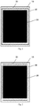
Fig. 1 is a schematic diagram showing a screen plate according to some embodiments of the present disclosure; -
Fig. 2 is a schematic diagram showing a screen plate according to some other embodiments of the present disclosure; -
Fig. 3 is a flow chart showing a packaging method according to some embodiments of the present disclosure; -
Fig. 4 is a schematic diagram showing a screen plate in the related art; -
Fig. 5 is a schematic diagram showing the appearance of a packaging adhesive formed by printing the packaging adhesive by using the screen plate shown inFig. 4 ; and -
Fig. 6 is a schematic diagram showing the appearance of a packaging adhesive formed by printing the packaging adhesive by using the screen plate according to the embodiments of the present disclosure. - In order to make objects, technical solutions and advantages of the embodiments of the present disclosure clearer, the technical solutions of the embodiments of the present disclosure will be clearly and completely described below in conjunction with the drawings of the embodiments of the present disclosure. It is apparent that the described embodiments are a part of the embodiments of the present disclosure, and not all of them. Based on the described embodiments of the present disclosure, all other embodiments obtained by those skilled in the art fall within the scope of the present disclosure.
- As shown in
Fig. 1 , some embodiments of the present disclosure provide a screen plate including aframe 10, amesh 20 fixed to theframe 10, and amasking film 30 arranged on themesh 20. A printing area is formed in a portion of themesh 20 that is not masked by themasking film 30. Amasking line 40 is arranged in the printing area. Themasking line 40 is arranged along an edge of themasking film 30. A width of themasking line 40 is greater than a width of each of mesh lines of themesh 20. - In the embodiments of the present disclosure, the printing area is an annular structure surrounding the
masking film 30, and themasking line 40 is a closed annular structure surrounding themasking film 30. - In the embodiment of the present disclosure, the printing area is provided with one
masking line 40 with the closed annular structure. Certainly, in some other embodiments of the present disclosure, the printing area may be provided with two ormore masking lines 40 of the closed annular structure. - In some other embodiments of the present disclosure, the
masking line 40 may also not be a closed annular structure. For example, as shown inFig. 2 , themasking line 40 includes four line segments that are arranged independently to each other, and each of the line segments is arranged along the edge of themasking film 30 corresponding to the line segment. In some other embodiments of the present disclosure, the number of the line segments in themasking line 40 may be less than four. For example, only one line segment is arranged in the printing areas on each of the left and right sides of themasking film 30. - Certainly, in embodiments where the
masking line 40 is not of a closed annular structure, the number of turns of themasking line 40 is not limited to one. - In the embodiments of the present disclosure, a distance between the masking
line 40 and the edge of theframe 10 corresponding to themasking line 40 is equal to a distance between the maskingline 40 and the edge of the maskingfilm 30 corresponding to maskingline 40. In other words, the maskingline 40 is located in the middle of an annular portion of the corresponding printing area. Certainly, in some other embodiments of the present disclosure, the maskingline 40 may not be arranged in the middle of the annular portion of the corresponding printing area. For example, the maskingline 40 is arranged closer to the edge of the maskingfilm 30, or is arranged closer to the edge of theframe 10 corresponding to themasking line 40. - In the embodiments of the present disclosure, the
mesh 20 is of a grid structure, is formed by mesh lines and has a plurality of mesh openings. The plurality of mesh openings is used to print a material to be printed, such as the packaging adhesive, onto a substrate to be printed. - Optionally, in the embodiments of the present disclosure, the masking
line 40 and the mesh lines of themesh 20 may be made of a same material, such as a metal material. - As shown in
Fig. 3 , some embodiments of the present disclosure further provide a packaging method, includingsteps 301 to 305. - Step 301: providing a screen plate, which is the screen plate in the above embodiments.
- Step 302: coating the printing area of the screen plate with a packaging adhesive. The packaging adhesive may be a glass adhesive.
- In some optional embodiments, the printing area of the screen plate may be coated with the packaging adhesive by a feeding scraper.
- Step 303: enabling the screen plate coated with the packaging adhesive to contact a first substrate to be printed, and printing the packaging adhesive onto the first substrate.
- In some optional embodiments, the screen plate may be fixed onto the to-be-printed first substrate by a fixed component of a packaging device. When preparing to print, the screen plate is coated with the packaging adhesive by the scraper so that the packaging adhesive contacts the first substrate through mesh openings of the printing area. After scraping the packaging adhesive by the scraper, the screen plate is moved down entirely, so that the packaging adhesive is printed onto the first substrate.
- Step 304: aligning the first substrate with a second substrate.
- Step 305: solidifying the packaging adhesive to form a packaging layer.
- The way of laser irradiation may be used to solidify the packaging adhesive.
- In the embodiments of the present disclosure, when the packaging adhesive is printed onto the to-be-printed substrate by using the screen plate, the packaging adhesive in the printing area corresponding to the masking line is less than the packaging adhesive in the printing area on both sides of the masking line, so that the height of the packaging adhesive in the area where the masking line is located is lower than the height of the packaging adhesive on both sides of the masking line. Thus, the packaging adhesive which has been printed has at least two retaining walls, which are respectively located on both sides of the packaging adhesive in the area where the masking line is located. At least two retaining walls may form a secondary protection or multiple protections for the display panel. Specifically, in the case that one of the retaining walls is eroded or cracked, the other retaining walls may still protect the display substrate, thereby achieving a better packaging effect and improving the resistance to erosion of the display panel.
- As shown in
Figs. 4 to 6 ,Fig. 4 is a schematic diagram showing a screen plate in the related art;Fig. 5 is a schematic diagram showing the appearance of a packaging adhesive formed by printing the packaging adhesive by using the screen plate as shown inFig. 4 ; andFig. 6 is a schematic diagram showing the appearance of a packaging adhesive formed by printing the packaging adhesive by using the screen plate of the embodiments of the present disclosure. It can be seen fromFig. 6 that after the packaging adhesive is printed through the screen plate according to the embodiment of the present disclosure, the appearance of the printed packaging adhesive is as follows: the height of thepackaging adhesive 61 in the area where the masking line is located is lower than the height of thepackaging adhesive 62 on both sides of the masking line to form the package adhesive having two retaining walls. A cross section of the packaging adhesive is of a hump-like shape. The two retaining walls may form a secondary protection for the display panel, thereby achieving a better packaging effect and improving the anti-erosion of the display panel. - Some embodiments of the present disclosure further provide a display panel which is packaged using the packaging method in the above embodiments. The display panel includes a first substrate, a second substrate, and a packaging layer between the first substrate and the second substrate. The packaging layer is an annular structure arranged surround a display area of the display panel. The packaging layer includes at least two retaining walls which are spaced from each other and arranged along an edge of the display area. A strip-shaped groove is formed between any two adjacent retaining walls.
- The packaging layer corresponds to the printing area in the above method embodiments. The strip-shaped groove is formed due to the
masking line 40 in the above method embodiments. - In an embodiment of the present disclosure, the packaging layer includes at least two retaining walls which are arranged along an edge of the display area and spaced from each other. Thus, the two retaining walls may form a secondary protection for the display panel, thereby achieving a better packaging effect and improving the erosion resistance of the display panel.
- Optionally, in an embodiment of the present disclosure, the packaging layer includes two retaining walls which are spaced from each other. The two retaining walls which are spaced from each other respectively form two closed annular structures which may enhance the packaging effect.
- In some optional embodiments of the present disclosure, the packaging layer may also include two or more retaining walls which are spaced from each other. The number of retaining walls is determined depending on the number of masking lines in the printing area in the above method embodiments.
- Optionally, in an embodiment of the present disclosure, inside the strip-shaped groove is a vacuum to prevent water, gas and the like from remaining in the packaging structure, thereby further improving the erosion resistance of the display panel. In addition, laser solidifying is usually performed on the packaging adhesive under atmospheric pressure. There is a pressure difference between the strip-shaped groove and the external atmospheric pressure, so that the packaging adhesive and the display substrate may be further pressed, and the packaging adhesive and the display substrate are combined more tightly so as to improve the packaging effect.
- In the embodiments of the present disclosure, the strip-shaped groove may further be filled with a water-absorbing material and a getter material. In the case that water and vapor enter the display panel through the external retaining wall, the water and vapor may be respectively absorbed by the water-absorbing material and the getter material, thereby further improving the erosion resistance of the display panel.
- Some embodiments of the present disclosure further provide a display device including the above display panel.
- Unless otherwise defined, technical terms or scientific terms used in the present disclosure should be interpreted according to common meanings thereof as commonly understood by those of ordinary skills in the art. Such terms as "first", "second" and the like used in the present disclosure do not represent any order, quantity or importance, but are merely used to distinguish different components. Similarly, such terms as "a" or "one" and the like do not indicate a quantity limitation, but mean that there is at least one. Such terms as "connected" or "interconnected" and the like are not limited to physical or mechanical connections, but may include electrical connections, whether direct connection or indirect connection. Such terms as "on", "under", "left", "right" and the like are only used to represent a relative position relationship, and when an absolute position of a described object is changed, the relative position relationship thereof may also be changed accordingly.
- The above embodiments are merely optional embodiments of the present disclosure. It should be noted that numerous improvements and modifications may be made by those skilled in the art without departing from the principle of the present disclosure, and these improvements and modifications shall also fall within the scope of the present disclosure.
Claims (15)
- A screen plate, comprising:
a frame, a mesh fixed onto the frame and a masking film arranged on the mesh, wherein a printing area is formed in a portion of the mesh that is not masked by the masking film, at least one masking line is arranged in the printing area along edges of the masking film, and a width of each of the at least one masking line is greater than a width of each mesh line of the mesh. - The screen plate according to claim 1, wherein
the printing area is an annular structure surrounding the masking film, and each of the at least one masking line is a closed annular structure surrounding the masking film. - The screen plate according to claim 2, wherein
the printing area is provided with one masking line of the closed annular structure. - The screen plate according to claim 1, wherein
the number of the at least one masking line is two, and the two masking lines are respectively located in the printing area corresponding to a left side and a right side of the masking film; or
the number of the at least one masking line is four, and each of the four masking lines is located in the printing area corresponding to one of the edges of the masking film. - The screen plate according to any one of claims 1 to 4, wherein
a distance between the masking line and each edge of the frame corresponding to the masking line is equal to a distance between the masking line and each edge of the masking film corresponding to masking line. - A packaging method, comprising
providing with the screen plate according to any one of claims 1 to 5;
coating the printing area of the screen plate with a packaging adhesive; and
enabling the screen plate coated with the packaging adhesive to contact a first substrate to be printed, and printing the packaging adhesive onto the first substrate. - The packaging method according to claim 6, further comprising:aligning the first substrate and a second substrate in different layers; andsolidifying the packaging adhesive to form a packaging layer.
- The packaging method according to claim 7, wherein
the formed packaging layer comprises a plurality of retaining walls that are spaced from each other; and a strip-shaped groove is formed between any two adjacent retaining walls of the retaining walls. - The packaging method according to claim 8, wherein
the strip-shaped groove is formed via each of the at least one masking line in the printing area. - A display panel, that is packaged by using the packaging method according to claim 6 or 7, comprising:
a first substrate, a second substrate, and a packaging layer between the first substrate and the second substrate, wherein the packaging layer is an annular structure arranged surrounding a display area of the display substrate; the packaging layer comprises at least two retaining walls that are spaced from each other and arranged along an edge of the display area; and a strip-shaped groove is formed between any two adjacent retaining walls of the retaining walls. - The display panel according to claim 10, wherein the strip-shaped groove is formed via each masking line in the printing area.
- The display panel according to claim 10, wherein
the packaging layer comprises two retaining walls that are spaced from each other, and each of the two retaining walls that are spaced from each other is of a closed annular structure. - The display panel according to claim 10, wherein a space inside the strip-shaped groove is a vacuum.
- The display panel according to claim 7, wherein the strip-shaped groove is filled with a water-absorbing material and a gas-absorbing material.
- A display device, comprising the display panel according to any one of claims 10 to 14.
Applications Claiming Priority (2)
| Application Number | Priority Date | Filing Date | Title |
|---|---|---|---|
| CN201710646231.3A CN107507923B (en) | 2017-08-01 | 2017-08-01 | A screen screen, packaging method, display panel and display device |
| PCT/CN2018/089217 WO2019024591A1 (en) | 2017-08-01 | 2018-05-31 | Screen printing plate, packaging method, display panel and display device |
Publications (3)
| Publication Number | Publication Date |
|---|---|
| EP3664176A1 true EP3664176A1 (en) | 2020-06-10 |
| EP3664176A4 EP3664176A4 (en) | 2021-05-12 |
| EP3664176B1 EP3664176B1 (en) | 2023-03-15 |
Family
ID=60690183
Family Applications (1)
| Application Number | Title | Priority Date | Filing Date |
|---|---|---|---|
| EP18841622.6A Active EP3664176B1 (en) | 2017-08-01 | 2018-05-31 | Screen printing plate, packaging method, display panel and display device |
Country Status (4)
| Country | Link |
|---|---|
| US (1) | US10749145B2 (en) |
| EP (1) | EP3664176B1 (en) |
| CN (1) | CN107507923B (en) |
| WO (1) | WO2019024591A1 (en) |
Families Citing this family (4)
| Publication number | Priority date | Publication date | Assignee | Title |
|---|---|---|---|---|
| CN107507923B (en) * | 2017-08-01 | 2019-12-03 | 京东方科技集团股份有限公司 | A screen screen, packaging method, display panel and display device |
| CN107742472B (en) * | 2017-09-25 | 2021-03-26 | 昆山国显光电有限公司 | Packaging mask plate, packaging method and display panel |
| CN109940773B (en) * | 2019-04-15 | 2021-01-26 | 苏州协鑫光伏科技有限公司 | Glue applying method of two-component glue |
| CN111016478A (en) * | 2019-11-14 | 2020-04-17 | 深圳市华星光电半导体显示技术有限公司 | Method for manufacturing perovskite color conversion film |
Family Cites Families (20)
| Publication number | Priority date | Publication date | Assignee | Title |
|---|---|---|---|---|
| JPH0691840A (en) * | 1992-09-16 | 1994-04-05 | Matsushita Electric Ind Co Ltd | Screen printing method and screen for printing |
| JP3111803B2 (en) * | 1994-05-19 | 2000-11-27 | 株式会社村田製作所 | Screen printing plate |
| JP3488413B2 (en) * | 2000-03-02 | 2004-01-19 | 株式会社三誠商會 | Printing screen plate and method of manufacturing printing screen plate |
| JP4356186B2 (en) * | 2000-03-30 | 2009-11-04 | 株式会社村田製作所 | Screen printing plate and manufacturing method thereof |
| JP3703446B2 (en) * | 2001-09-13 | 2005-10-05 | パイオニア株式会社 | Screen plate and screen printing method using the same |
| GB2383683B (en) * | 2001-12-28 | 2004-04-07 | Delta Optoelectronics Inc | Housing structure with multiple sealing layers |
| JP3884351B2 (en) * | 2002-08-26 | 2007-02-21 | 株式会社 日立ディスプレイズ | Image display device and manufacturing method thereof |
| JP2005340020A (en) | 2004-05-27 | 2005-12-08 | Hitachi Displays Ltd | Organic electroluminescent display device and manufacturing method of the same |
| US8258696B2 (en) * | 2007-06-28 | 2012-09-04 | Samsung Mobile Display Co., Ltd. | Light emitting display and method of manufacturing the same |
| WO2010007656A1 (en) | 2008-07-14 | 2010-01-21 | パイオニア株式会社 | Organic el panel and its manufacturing method |
| CN102854666B (en) | 2012-07-23 | 2015-11-25 | 北京京东方光电科技有限公司 | A kind of liquid crystal panel and liquid crystal indicator |
| CN104290433B (en) | 2014-09-03 | 2020-04-10 | 安徽省大富光电科技有限公司 | Screen unit for printing and method for manufacturing the same |
| CN204278722U (en) * | 2014-12-08 | 2015-04-22 | 京东方科技集团股份有限公司 | A kind of half tone and display device |
| JP2017013330A (en) * | 2015-06-30 | 2017-01-19 | 太陽誘電ケミカルテクノロジー株式会社 | Stencil for printing and manufacturing method therefor |
| CN104966726A (en) * | 2015-07-03 | 2015-10-07 | 深圳市华星光电技术有限公司 | OLED display panel and packaging method thereof |
| CN105058957B (en) | 2015-07-27 | 2018-12-28 | 京东方科技集团股份有限公司 | Halftone and preparation method thereof, packaging method, display panel, display device |
| US20170271615A1 (en) | 2015-09-15 | 2017-09-21 | Boe Technology Group Co., Ltd. | Screen-printing mask, method for fabricating the same, and related packaging method |
| CN105810849B (en) * | 2016-03-17 | 2018-03-30 | 深圳市华星光电技术有限公司 | The method for packing of substrate |
| CN106876428B (en) * | 2017-02-03 | 2019-10-08 | 上海天马微电子有限公司 | flexible display panel, manufacturing method thereof and display device |
| CN107507923B (en) | 2017-08-01 | 2019-12-03 | 京东方科技集团股份有限公司 | A screen screen, packaging method, display panel and display device |
-
2017
- 2017-08-01 CN CN201710646231.3A patent/CN107507923B/en active Active
-
2018
- 2018-05-31 EP EP18841622.6A patent/EP3664176B1/en active Active
- 2018-05-31 WO PCT/CN2018/089217 patent/WO2019024591A1/en not_active Ceased
- 2018-05-31 US US16/335,905 patent/US10749145B2/en active Active
Also Published As
| Publication number | Publication date |
|---|---|
| CN107507923B (en) | 2019-12-03 |
| EP3664176B1 (en) | 2023-03-15 |
| US10749145B2 (en) | 2020-08-18 |
| CN107507923A (en) | 2017-12-22 |
| WO2019024591A1 (en) | 2019-02-07 |
| US20190267577A1 (en) | 2019-08-29 |
| EP3664176A4 (en) | 2021-05-12 |
Similar Documents
| Publication | Publication Date | Title |
|---|---|---|
| US10749145B2 (en) | Screen plate, packaging method, display panel and display device | |
| US9876191B2 (en) | OLED panel, packaging method thereof, and a display device | |
| CN106816456B (en) | An organic light emitting diode display panel and display | |
| EP3678205B1 (en) | Oled display mother board and manufacturing method thereof, manufacturing method of oled display panel and oled display device thereof | |
| US9947730B2 (en) | Flexible display device and method for packaging the same | |
| US10109810B2 (en) | Flexible display panel, package method thereof and display device | |
| US9614185B2 (en) | Display panel, manufacturing method thereof, and display device | |
| US20170222181A1 (en) | Display device | |
| US20160141550A1 (en) | Packaging method of organic light emitting display panel, organic light emitting display panel and display device | |
| US10409104B2 (en) | Display substrate and display device | |
| US20160329528A1 (en) | Oled panel,l method for fabricating the same, screen printing plate, display device | |
| US20210026404A1 (en) | Display panel, hole forming method, and electronic equipment | |
| US10074821B2 (en) | Screen-printing mask, related packaging method, display panel, display apparatus, and method for fabricating the same | |
| CN105676546A (en) | Display substrate, display device and spraying device | |
| US20170294623A1 (en) | Packaging method, display panel and display device | |
| US10908331B2 (en) | Display substrate, manufacturing method thereof and display panel | |
| US20160365538A1 (en) | Packaging structure of oled device and packaging method thereof | |
| US20160260925A1 (en) | Organic electroluminescent device and method for preparing the same, and display apparatus | |
| KR20200042007A (en) | Liquid crystal display assembly | |
| US20210140031A1 (en) | Open mask, open mask assembly, and evaporation method using the open mask | |
| US11609618B2 (en) | Display motherboard and manufacturing method thereof | |
| US20190165328A1 (en) | Display panel and manufacturing method thereof | |
| EP4116763A1 (en) | Display device | |
| CN212967755U (en) | Packaging cover plate, silicon-based organic light-emitting display panel and display device | |
| US10490578B2 (en) | Array substrate, display panel and manufacturing method thereof |
Legal Events
| Date | Code | Title | Description |
|---|---|---|---|
| STAA | Information on the status of an ep patent application or granted ep patent |
Free format text: STATUS: THE INTERNATIONAL PUBLICATION HAS BEEN MADE |
|
| PUAI | Public reference made under article 153(3) epc to a published international application that has entered the european phase |
Free format text: ORIGINAL CODE: 0009012 |
|
| STAA | Information on the status of an ep patent application or granted ep patent |
Free format text: STATUS: REQUEST FOR EXAMINATION WAS MADE |
|
| 17P | Request for examination filed |
Effective date: 20190325 |
|
| AK | Designated contracting states |
Kind code of ref document: A1 Designated state(s): AL AT BE BG CH CY CZ DE DK EE ES FI FR GB GR HR HU IE IS IT LI LT LU LV MC MK MT NL NO PL PT RO RS SE SI SK SM TR |
|
| AX | Request for extension of the european patent |
Extension state: BA ME |
|
| DAV | Request for validation of the european patent (deleted) | ||
| DAX | Request for extension of the european patent (deleted) | ||
| A4 | Supplementary search report drawn up and despatched |
Effective date: 20210412 |
|
| RIC1 | Information provided on ipc code assigned before grant |
Ipc: H01L 51/52 20060101AFI20210406BHEP Ipc: B41F 15/36 20060101ALI20210406BHEP |
|
| GRAP | Despatch of communication of intention to grant a patent |
Free format text: ORIGINAL CODE: EPIDOSNIGR1 |
|
| STAA | Information on the status of an ep patent application or granted ep patent |
Free format text: STATUS: GRANT OF PATENT IS INTENDED |
|
| RIC1 | Information provided on ipc code assigned before grant |
Ipc: B41F 15/36 20060101ALI20221130BHEP Ipc: H01L 51/52 20060101AFI20221130BHEP |
|
| INTG | Intention to grant announced |
Effective date: 20221215 |
|
| GRAS | Grant fee paid |
Free format text: ORIGINAL CODE: EPIDOSNIGR3 |
|
| GRAA | (expected) grant |
Free format text: ORIGINAL CODE: 0009210 |
|
| STAA | Information on the status of an ep patent application or granted ep patent |
Free format text: STATUS: THE PATENT HAS BEEN GRANTED |
|
| AK | Designated contracting states |
Kind code of ref document: B1 Designated state(s): AL AT BE BG CH CY CZ DE DK EE ES FI FR GB GR HR HU IE IS IT LI LT LU LV MC MK MT NL NO PL PT RO RS SE SI SK SM TR |
|
| REG | Reference to a national code |
Ref country code: CH Ref legal event code: EP Ref country code: GB Ref legal event code: FG4D |
|
| REG | Reference to a national code |
Ref country code: DE Ref legal event code: R096 Ref document number: 602018047313 Country of ref document: DE |
|
| REG | Reference to a national code |
Ref country code: IE Ref legal event code: FG4D |
|
| REG | Reference to a national code |
Ref country code: AT Ref legal event code: REF Ref document number: 1554506 Country of ref document: AT Kind code of ref document: T Effective date: 20230415 |
|
| REG | Reference to a national code |
Ref country code: LT Ref legal event code: MG9D |
|
| REG | Reference to a national code |
Ref country code: NL Ref legal event code: MP Effective date: 20230315 |
|
| PG25 | Lapsed in a contracting state [announced via postgrant information from national office to epo] |
Ref country code: RS Free format text: LAPSE BECAUSE OF FAILURE TO SUBMIT A TRANSLATION OF THE DESCRIPTION OR TO PAY THE FEE WITHIN THE PRESCRIBED TIME-LIMIT Effective date: 20230315 Ref country code: NO Free format text: LAPSE BECAUSE OF FAILURE TO SUBMIT A TRANSLATION OF THE DESCRIPTION OR TO PAY THE FEE WITHIN THE PRESCRIBED TIME-LIMIT Effective date: 20230615 Ref country code: LV Free format text: LAPSE BECAUSE OF FAILURE TO SUBMIT A TRANSLATION OF THE DESCRIPTION OR TO PAY THE FEE WITHIN THE PRESCRIBED TIME-LIMIT Effective date: 20230315 Ref country code: LT Free format text: LAPSE BECAUSE OF FAILURE TO SUBMIT A TRANSLATION OF THE DESCRIPTION OR TO PAY THE FEE WITHIN THE PRESCRIBED TIME-LIMIT Effective date: 20230315 Ref country code: HR Free format text: LAPSE BECAUSE OF FAILURE TO SUBMIT A TRANSLATION OF THE DESCRIPTION OR TO PAY THE FEE WITHIN THE PRESCRIBED TIME-LIMIT Effective date: 20230315 |
|
| REG | Reference to a national code |
Ref country code: AT Ref legal event code: MK05 Ref document number: 1554506 Country of ref document: AT Kind code of ref document: T Effective date: 20230315 |
|
| PG25 | Lapsed in a contracting state [announced via postgrant information from national office to epo] |
Ref country code: SE Free format text: LAPSE BECAUSE OF FAILURE TO SUBMIT A TRANSLATION OF THE DESCRIPTION OR TO PAY THE FEE WITHIN THE PRESCRIBED TIME-LIMIT Effective date: 20230315 Ref country code: NL Free format text: LAPSE BECAUSE OF FAILURE TO SUBMIT A TRANSLATION OF THE DESCRIPTION OR TO PAY THE FEE WITHIN THE PRESCRIBED TIME-LIMIT Effective date: 20230315 Ref country code: GR Free format text: LAPSE BECAUSE OF FAILURE TO SUBMIT A TRANSLATION OF THE DESCRIPTION OR TO PAY THE FEE WITHIN THE PRESCRIBED TIME-LIMIT Effective date: 20230616 Ref country code: FI Free format text: LAPSE BECAUSE OF FAILURE TO SUBMIT A TRANSLATION OF THE DESCRIPTION OR TO PAY THE FEE WITHIN THE PRESCRIBED TIME-LIMIT Effective date: 20230315 |
|
| PG25 | Lapsed in a contracting state [announced via postgrant information from national office to epo] |
Ref country code: SM Free format text: LAPSE BECAUSE OF FAILURE TO SUBMIT A TRANSLATION OF THE DESCRIPTION OR TO PAY THE FEE WITHIN THE PRESCRIBED TIME-LIMIT Effective date: 20230315 Ref country code: RO Free format text: LAPSE BECAUSE OF FAILURE TO SUBMIT A TRANSLATION OF THE DESCRIPTION OR TO PAY THE FEE WITHIN THE PRESCRIBED TIME-LIMIT Effective date: 20230315 Ref country code: PT Free format text: LAPSE BECAUSE OF FAILURE TO SUBMIT A TRANSLATION OF THE DESCRIPTION OR TO PAY THE FEE WITHIN THE PRESCRIBED TIME-LIMIT Effective date: 20230717 Ref country code: ES Free format text: LAPSE BECAUSE OF FAILURE TO SUBMIT A TRANSLATION OF THE DESCRIPTION OR TO PAY THE FEE WITHIN THE PRESCRIBED TIME-LIMIT Effective date: 20230315 Ref country code: EE Free format text: LAPSE BECAUSE OF FAILURE TO SUBMIT A TRANSLATION OF THE DESCRIPTION OR TO PAY THE FEE WITHIN THE PRESCRIBED TIME-LIMIT Effective date: 20230315 Ref country code: CZ Free format text: LAPSE BECAUSE OF FAILURE TO SUBMIT A TRANSLATION OF THE DESCRIPTION OR TO PAY THE FEE WITHIN THE PRESCRIBED TIME-LIMIT Effective date: 20230315 Ref country code: AT Free format text: LAPSE BECAUSE OF FAILURE TO SUBMIT A TRANSLATION OF THE DESCRIPTION OR TO PAY THE FEE WITHIN THE PRESCRIBED TIME-LIMIT Effective date: 20230315 |
|
| PG25 | Lapsed in a contracting state [announced via postgrant information from national office to epo] |
Ref country code: SK Free format text: LAPSE BECAUSE OF FAILURE TO SUBMIT A TRANSLATION OF THE DESCRIPTION OR TO PAY THE FEE WITHIN THE PRESCRIBED TIME-LIMIT Effective date: 20230315 Ref country code: PL Free format text: LAPSE BECAUSE OF FAILURE TO SUBMIT A TRANSLATION OF THE DESCRIPTION OR TO PAY THE FEE WITHIN THE PRESCRIBED TIME-LIMIT Effective date: 20230315 Ref country code: IS Free format text: LAPSE BECAUSE OF FAILURE TO SUBMIT A TRANSLATION OF THE DESCRIPTION OR TO PAY THE FEE WITHIN THE PRESCRIBED TIME-LIMIT Effective date: 20230715 |
|
| REG | Reference to a national code |
Ref country code: DE Ref legal event code: R097 Ref document number: 602018047313 Country of ref document: DE |
|
| REG | Reference to a national code |
Ref country code: CH Ref legal event code: PL |
|
| PG25 | Lapsed in a contracting state [announced via postgrant information from national office to epo] |
Ref country code: MC Free format text: LAPSE BECAUSE OF FAILURE TO SUBMIT A TRANSLATION OF THE DESCRIPTION OR TO PAY THE FEE WITHIN THE PRESCRIBED TIME-LIMIT Effective date: 20230315 |
|
| PLBE | No opposition filed within time limit |
Free format text: ORIGINAL CODE: 0009261 |
|
| STAA | Information on the status of an ep patent application or granted ep patent |
Free format text: STATUS: NO OPPOSITION FILED WITHIN TIME LIMIT |
|
| REG | Reference to a national code |
Ref country code: BE Ref legal event code: MM Effective date: 20230531 |
|
| PG25 | Lapsed in a contracting state [announced via postgrant information from national office to epo] |
Ref country code: SI Free format text: LAPSE BECAUSE OF FAILURE TO SUBMIT A TRANSLATION OF THE DESCRIPTION OR TO PAY THE FEE WITHIN THE PRESCRIBED TIME-LIMIT Effective date: 20230315 Ref country code: MC Free format text: LAPSE BECAUSE OF FAILURE TO SUBMIT A TRANSLATION OF THE DESCRIPTION OR TO PAY THE FEE WITHIN THE PRESCRIBED TIME-LIMIT Effective date: 20230315 Ref country code: LU Free format text: LAPSE BECAUSE OF NON-PAYMENT OF DUE FEES Effective date: 20230531 Ref country code: LI Free format text: LAPSE BECAUSE OF NON-PAYMENT OF DUE FEES Effective date: 20230531 Ref country code: DK Free format text: LAPSE BECAUSE OF FAILURE TO SUBMIT A TRANSLATION OF THE DESCRIPTION OR TO PAY THE FEE WITHIN THE PRESCRIBED TIME-LIMIT Effective date: 20230315 Ref country code: CH Free format text: LAPSE BECAUSE OF NON-PAYMENT OF DUE FEES Effective date: 20230531 |
|
| 26N | No opposition filed |
Effective date: 20231218 |
|
| GBPC | Gb: european patent ceased through non-payment of renewal fee |
Effective date: 20230615 |
|
| REG | Reference to a national code |
Ref country code: IE Ref legal event code: MM4A |
|
| PG25 | Lapsed in a contracting state [announced via postgrant information from national office to epo] |
Ref country code: IE Free format text: LAPSE BECAUSE OF NON-PAYMENT OF DUE FEES Effective date: 20230531 |
|
| PG25 | Lapsed in a contracting state [announced via postgrant information from national office to epo] |
Ref country code: IE Free format text: LAPSE BECAUSE OF NON-PAYMENT OF DUE FEES Effective date: 20230531 Ref country code: GB Free format text: LAPSE BECAUSE OF NON-PAYMENT OF DUE FEES Effective date: 20230615 |
|
| PG25 | Lapsed in a contracting state [announced via postgrant information from national office to epo] |
Ref country code: IT Free format text: LAPSE BECAUSE OF FAILURE TO SUBMIT A TRANSLATION OF THE DESCRIPTION OR TO PAY THE FEE WITHIN THE PRESCRIBED TIME-LIMIT Effective date: 20230315 Ref country code: FR Free format text: LAPSE BECAUSE OF NON-PAYMENT OF DUE FEES Effective date: 20230531 Ref country code: BE Free format text: LAPSE BECAUSE OF NON-PAYMENT OF DUE FEES Effective date: 20230531 |
|
| PGFP | Annual fee paid to national office [announced via postgrant information from national office to epo] |
Ref country code: DE Payment date: 20240517 Year of fee payment: 7 |
|
| PG25 | Lapsed in a contracting state [announced via postgrant information from national office to epo] |
Ref country code: BG Free format text: LAPSE BECAUSE OF FAILURE TO SUBMIT A TRANSLATION OF THE DESCRIPTION OR TO PAY THE FEE WITHIN THE PRESCRIBED TIME-LIMIT Effective date: 20230315 |
|
| PG25 | Lapsed in a contracting state [announced via postgrant information from national office to epo] |
Ref country code: BG Free format text: LAPSE BECAUSE OF FAILURE TO SUBMIT A TRANSLATION OF THE DESCRIPTION OR TO PAY THE FEE WITHIN THE PRESCRIBED TIME-LIMIT Effective date: 20230315 |
|
| PG25 | Lapsed in a contracting state [announced via postgrant information from national office to epo] |
Ref country code: CY Free format text: LAPSE BECAUSE OF FAILURE TO SUBMIT A TRANSLATION OF THE DESCRIPTION OR TO PAY THE FEE WITHIN THE PRESCRIBED TIME-LIMIT; INVALID AB INITIO Effective date: 20180531 |
|
| PG25 | Lapsed in a contracting state [announced via postgrant information from national office to epo] |
Ref country code: HU Free format text: LAPSE BECAUSE OF FAILURE TO SUBMIT A TRANSLATION OF THE DESCRIPTION OR TO PAY THE FEE WITHIN THE PRESCRIBED TIME-LIMIT; INVALID AB INITIO Effective date: 20180531 |
|
| REG | Reference to a national code |
Ref country code: DE Ref legal event code: R119 Ref document number: 602018047313 Country of ref document: DE |
|
| PG25 | Lapsed in a contracting state [announced via postgrant information from national office to epo] |
Ref country code: TR Free format text: LAPSE BECAUSE OF FAILURE TO SUBMIT A TRANSLATION OF THE DESCRIPTION OR TO PAY THE FEE WITHIN THE PRESCRIBED TIME-LIMIT Effective date: 20230315 |
|
| PG25 | Lapsed in a contracting state [announced via postgrant information from national office to epo] |
Ref country code: DE Free format text: LAPSE BECAUSE OF NON-PAYMENT OF DUE FEES Effective date: 20251202 |