EP3660923A1 - Method for manufacturing an ohmic contact for a hemt device - Google Patents
Method for manufacturing an ohmic contact for a hemt device Download PDFInfo
- Publication number
- EP3660923A1 EP3660923A1 EP19212334.7A EP19212334A EP3660923A1 EP 3660923 A1 EP3660923 A1 EP 3660923A1 EP 19212334 A EP19212334 A EP 19212334A EP 3660923 A1 EP3660923 A1 EP 3660923A1
- Authority
- EP
- European Patent Office
- Prior art keywords
- layer
- forming
- photoresist layer
- semiconductor body
- sacrificial
- Prior art date
- Legal status (The legal status is an assumption and is not a legal conclusion. Google has not performed a legal analysis and makes no representation as to the accuracy of the status listed.)
- Granted
Links
Images


Classifications
-
- H—ELECTRICITY
- H10—SEMICONDUCTOR DEVICES; ELECTRIC SOLID-STATE DEVICES NOT OTHERWISE PROVIDED FOR
- H10D—INORGANIC ELECTRIC SEMICONDUCTOR DEVICES
- H10D30/00—Field-effect transistors [FET]
- H10D30/01—Manufacture or treatment
- H10D30/015—Manufacture or treatment of FETs having heterojunction interface channels or heterojunction gate electrodes, e.g. HEMT
-
- H—ELECTRICITY
- H10—SEMICONDUCTOR DEVICES; ELECTRIC SOLID-STATE DEVICES NOT OTHERWISE PROVIDED FOR
- H10D—INORGANIC ELECTRIC SEMICONDUCTOR DEVICES
- H10D64/00—Electrodes of devices having potential barriers
- H10D64/01—Manufacture or treatment
- H10D64/011—Manufacture or treatment of electrodes ohmically coupled to a semiconductor
-
- H—ELECTRICITY
- H10—SEMICONDUCTOR DEVICES; ELECTRIC SOLID-STATE DEVICES NOT OTHERWISE PROVIDED FOR
- H10D—INORGANIC ELECTRIC SEMICONDUCTOR DEVICES
- H10D30/00—Field-effect transistors [FET]
- H10D30/40—FETs having zero-dimensional [0D], one-dimensional [1D] or two-dimensional [2D] charge carrier gas channels
- H10D30/47—FETs having zero-dimensional [0D], one-dimensional [1D] or two-dimensional [2D] charge carrier gas channels having two-dimensional [2D] charge carrier gas channels, e.g. nanoribbon FETs or high electron mobility transistors [HEMT]
- H10D30/471—High electron mobility transistors [HEMT] or high hole mobility transistors [HHMT]
- H10D30/475—High electron mobility transistors [HEMT] or high hole mobility transistors [HHMT] having wider bandgap layer formed on top of lower bandgap active layer, e.g. undoped barrier HEMTs such as i-AlGaN/GaN HEMTs
-
- H—ELECTRICITY
- H10—SEMICONDUCTOR DEVICES; ELECTRIC SOLID-STATE DEVICES NOT OTHERWISE PROVIDED FOR
- H10D—INORGANIC ELECTRIC SEMICONDUCTOR DEVICES
- H10D30/00—Field-effect transistors [FET]
- H10D30/40—FETs having zero-dimensional [0D], one-dimensional [1D] or two-dimensional [2D] charge carrier gas channels
- H10D30/47—FETs having zero-dimensional [0D], one-dimensional [1D] or two-dimensional [2D] charge carrier gas channels having two-dimensional [2D] charge carrier gas channels, e.g. nanoribbon FETs or high electron mobility transistors [HEMT]
- H10D30/471—High electron mobility transistors [HEMT] or high hole mobility transistors [HHMT]
- H10D30/475—High electron mobility transistors [HEMT] or high hole mobility transistors [HHMT] having wider bandgap layer formed on top of lower bandgap active layer, e.g. undoped barrier HEMTs such as i-AlGaN/GaN HEMTs
- H10D30/4755—High electron mobility transistors [HEMT] or high hole mobility transistors [HHMT] having wider bandgap layer formed on top of lower bandgap active layer, e.g. undoped barrier HEMTs such as i-AlGaN/GaN HEMTs having wide bandgap charge-carrier supplying layers, e.g. modulation doped HEMTs such as n-AlGaAs/GaAs HEMTs
-
- H—ELECTRICITY
- H10—SEMICONDUCTOR DEVICES; ELECTRIC SOLID-STATE DEVICES NOT OTHERWISE PROVIDED FOR
- H10D—INORGANIC ELECTRIC SEMICONDUCTOR DEVICES
- H10D64/00—Electrodes of devices having potential barriers
- H10D64/01—Manufacture or treatment
-
- H—ELECTRICITY
- H10—SEMICONDUCTOR DEVICES; ELECTRIC SOLID-STATE DEVICES NOT OTHERWISE PROVIDED FOR
- H10D—INORGANIC ELECTRIC SEMICONDUCTOR DEVICES
- H10D64/00—Electrodes of devices having potential barriers
- H10D64/01—Manufacture or treatment
- H10D64/011—Manufacture or treatment of electrodes ohmically coupled to a semiconductor
- H10D64/0116—Manufacture or treatment of electrodes ohmically coupled to a semiconductor to Group III-V semiconductors
-
- H—ELECTRICITY
- H10—SEMICONDUCTOR DEVICES; ELECTRIC SOLID-STATE DEVICES NOT OTHERWISE PROVIDED FOR
- H10D—INORGANIC ELECTRIC SEMICONDUCTOR DEVICES
- H10D64/00—Electrodes of devices having potential barriers
- H10D64/20—Electrodes characterised by their shapes, relative sizes or dispositions
- H10D64/23—Electrodes carrying the current to be rectified, amplified, oscillated or switched, e.g. sources, drains, anodes or cathodes
- H10D64/251—Source or drain electrodes for field-effect devices
-
- H—ELECTRICITY
- H10—SEMICONDUCTOR DEVICES; ELECTRIC SOLID-STATE DEVICES NOT OTHERWISE PROVIDED FOR
- H10D—INORGANIC ELECTRIC SEMICONDUCTOR DEVICES
- H10D64/00—Electrodes of devices having potential barriers
- H10D64/20—Electrodes characterised by their shapes, relative sizes or dispositions
- H10D64/23—Electrodes carrying the current to be rectified, amplified, oscillated or switched, e.g. sources, drains, anodes or cathodes
- H10D64/251—Source or drain electrodes for field-effect devices
- H10D64/256—Source or drain electrodes for field-effect devices for lateral devices wherein the source or drain electrodes are recessed in semiconductor bodies
-
- H—ELECTRICITY
- H10—SEMICONDUCTOR DEVICES; ELECTRIC SOLID-STATE DEVICES NOT OTHERWISE PROVIDED FOR
- H10D—INORGANIC ELECTRIC SEMICONDUCTOR DEVICES
- H10D64/00—Electrodes of devices having potential barriers
- H10D64/60—Electrodes characterised by their materials
- H10D64/62—Electrodes ohmically coupled to a semiconductor
-
- H—ELECTRICITY
- H10—SEMICONDUCTOR DEVICES; ELECTRIC SOLID-STATE DEVICES NOT OTHERWISE PROVIDED FOR
- H10P—GENERIC PROCESSES OR APPARATUS FOR THE MANUFACTURE OR TREATMENT OF DEVICES COVERED BY CLASS H10
- H10P10/00—Bonding of wafers, substrates or parts of devices
-
- H—ELECTRICITY
- H10—SEMICONDUCTOR DEVICES; ELECTRIC SOLID-STATE DEVICES NOT OTHERWISE PROVIDED FOR
- H10D—INORGANIC ELECTRIC SEMICONDUCTOR DEVICES
- H10D62/00—Semiconductor bodies, or regions thereof, of devices having potential barriers
- H10D62/80—Semiconductor bodies, or regions thereof, of devices having potential barriers characterised by the materials
- H10D62/85—Semiconductor bodies, or regions thereof, of devices having potential barriers characterised by the materials being Group III-V materials, e.g. GaAs
- H10D62/8503—Nitride Group III-V materials, e.g. AlN or GaN
Definitions
- the present invention relates to a method for manufacturing an ohmic contact for a field-effect transistor with high electron mobility, known as HEMT (High Electron Mobility Transistor).
- HEMT High Electron Mobility Transistor
- the present invention discusses a procedure for self-alignment of a gold-free ohmic contact, which can be applied, for example, to source contacts and drain contacts of the HEMT device.
- a HEMT device comprises a heterostructure that has an interface between two different semiconductor materials, such as aluminium and gallium nitride (AlGaN) and gallium nitride (GaN).
- AlGaN aluminium and gallium nitride
- GaN gallium nitride
- 2DEG 2D electron gas
- the 2DEG layer represents an electron cloud with high charge density in which the charges possess high mobility. Such properties render the HEMT device attractive for radiofrequency (RF) applications and in power electronics.
- RF radiofrequency
- the HEMT device comprises ohmic contacts for the source and drain terminals that are made of gold so as to enable low contact and access resistances to be achieved (c.f. myselfo Iucolano, Giuseppe Greco, and Fabrizio Roccaforte - Applied Physics Letters 103, 201604 (2013); doi: 10.1063/1.4828839 ).
- the method for manufacturing gold ohmic contacts typically includes deposition of a sequence of metal layers on a semiconductor body formed by a stack including a substrate, a GaN layer and an AlGaN layer.
- the GaN and AlGaN layers form the heterostructure.
- the above sequence of metal layers is obtained with known processes (such as lithographic and lift-off steps) and comprises a titanium (Ti) layer in contact with the surface of the semiconductor body, an aluminium (Al) layer on the titanium layer, a nickel (Ni) layer on the aluminium layer, and a deposition of gold (Au) on the nickel layer.
- the first three layers referred to above are adapted, in a known way, to promote adhesion of the gold (which functions as central body of the ohmic contact) to the semiconductor body.
- the method for manufacturing gold ohmic contacts requires a thermal annealing process at high temperatures (for example, higher than 800°C). In these temperature conditions, Ti reacts with the N 2 available in the GaN, to form titanium nitride. Charge transport is thus guided by a metal-like behaviour of TiN due to intrusions of the metal in the 2DEG region. Formation of a gold contact is not in any case easy to implement on a CMOS line on account of the metallic contamination generated by gold, which would require dedicated equipment and segregated production areas.
- a commonly used alternative approach is to resort to gold-free ohmic contacts, where the central body of the ohmic contact is made of titanium and aluminium.
- the absence of gold in the ohmic contacts enables reduction of the annealing temperature to 600°C and use of techniques such as rapid thermal annealing (RTA).
- RTA rapid thermal annealing
- the RTA technique reduces the mechanical stresses to which the semiconductor body with ohmic contact is subjected and prevents formation of states of charge trap, thus improving the efficiency and productivity of the manufacturing process and of the HEMT device itself.
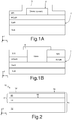
- Figure 1A shows an ohmic-contact structure 4 in a HEMT device of a known type, with non-recessed semiconductor body 2 ( Jing-Neng Yao, et al., "An Au-free GaN High Electron Mobility Transistor with Ti/Al/W Ohmic Metal Structure", IEEE, 2015 ).
- Figure 1B shows an ohmic-contact structure 6 in a HEMT device of a known type, with recessed semiconductor body 7 ( W. H. Tham, et al., "AlxGa1-xN/GaN MISHEMTs with a common gold-free metal-stack for source/drain/gate", IEEE ELECTRON DEVICE LETTERS, VOL. 36, No. 12, DECEMBER 2015 ).
- a dielectric layer 8, for example of SiN, extends over the semiconductor body 7.
- the ohmic contact 6 extends through the dielectric layer 8.
- passivating material here, SiN
- SiN passivating material
- the patent document US2004/094759 refers to a process for the manufacturing of ultra-low contact resistances in Gan-based HEMT devices.
- the process provides for an annealing of the contact metallisations at a high temperature, with the relative metallisations that penetrate inside the semiconductor body, thus making the structure peculiar.
- the use of gold makes the process unsuitable in CMOS production lines.
- the aim of the present invention is to provide a method for manufacturing an ohmic contact for a HEMT device that will overcome the limitations of the prior art.
- a method for manufacturing an ohmic contact for a HEMT device is provided, as defined in claim 1.
- Figures 2-6 illustrate, in a side section view, in a triaxial cartesian reference system X, Y, Z, manufacturing steps for obtaining an ohmic-contact structure 10, of a recessed type, illustrated, as a whole, in Figure 6 .
- the structure 1 forms part of a HEMT device.
- a substrate 12 of semiconductor material such as silicon, or silicon carbide (SiC), or sapphire (Al 2 O 3 ), or some other material, is provided.
- a first structural layer 14 in particular of intrinsic gallium nitride (GaN) (channel layer of the HEMT device), grown, for example epitaxially, on the substrate 12; a second structural layer 16, in particular of intrinsic aluminium and gallium nitride (AlGaN) or, more in general, of compounds based upon ternary or quaternary alloys of gallium nitride, such as Al x Ga 1-x N, AlInGaN, In x Ga 1-x N, Al x In 1-x Al (barrier layer of the HEMT device), grown, for example epitaxially, on the channel layer 14; and optionally a protection layer 18, in particular of GaN with a thickness of just a few nanometres (e.g., 1-4 nm), having the function of protecting the barrier layer 16 from oxidation phenomena.
- GaN intrinsic gallium nitride
- AlGaN intrinsic aluminium and gallium nitride
- AlGaN aluminum aluminium and gallium
- the channel layer 14 and the barrier layer 16 form, in a way in itself known, a heterostructure 17.
- one or more further buffer layers may be present, according to the need.
- the channel layer 14 has a thickness (along the axis Z), for example approximately between 1 ⁇ m and 5 ⁇ m; the barrier layer 16 has a thickness (along the axis Z), for example approximately between 5 nm and 30 nm.
- a 2DEG layer 15 is formed at the interface between the channel layer 14 and the barrier layer 16.
- the charge carriers belonging to the 2DEG are free to move in any direction in a plane XY (defined by the axes X and Y) at the 2DEG interface 15, whereas they are confined along the axis Z.
- the substrate 12, the channel layer 14, the barrier layer 16, and the protection layer 18 form a semiconductor body 5.
- a photoresist layer 28 with a thickness, for example, of between 1 and 3 ⁇ m is deposited. Said photoresist layer 28 entirely and evenly coats the epitaxial layer 18.
- the mask 30 is such that a region 34 of the photoresist layer 28 is exposed. Said region 34 defines the region in which the ohmic contact will be provided.
- an etch is then carried out (represented by arrows 40) for selective removal of portions of the protection layer 18 and of the underlying barrier layer 16, which are exposed through the trench 35. More in particular, the etching process comprises a first step, for removing the protection layer 18, and a second step, for partly or completely removing the barrier layer 16. Both of these steps use a Cl 2 -based chemistry.
- the photoresist layer 28 functions as etching mask, for protecting the regions of the semiconductor body 5 not exposed through the trench 35.
- the semiconductor body 5 is then dug further, to form a contact trench 42, which extends in depth in the barrier layer 16, terminating inside the barrier layer 16 itself.
- the contact trench 42 is delimited underneath by a bottom surface 44 of the barrier layer 16.
- the contact trench 42 is adapted to house an ohmic contact, as described hereinafter.
- the first etching step is designed to remove the protection layer 18 throughout its entire thickness in the area exposed by the trench 35, whereas the second etching step is designed to remove only part of the thickness, along Z, of the barrier layer 16. It is evident that, in the absence of the protection layer 18, which is optional, the etching process 40 comprises a single etching step for removing selective portions of the barrier layer 16.
- the contact trench 42 may extend throughout the entire thickness of the barrier layer 16, terminating at the interface with the underlying layer (here, the substrate 12), or else proceeding into the underlying layer, according to the design needs and parameters.
- Formation of the stack of metal layers comprises, according to one embodiment, forming a first interface layer 22a and a filling layer 22b on the interface layer 22a.
- the interface layer 22a is made of a material chosen from titanium or tantalum.
- the filling layer 22b is, in particular, made of aluminium.
- Formation of the stack of metal layers comprises, according to a further embodiment, forming in succession a first titanium or tantalum layer, an aluminium layer, and a second layer, which is also made of titanium or tantalum.
- the Ti layer is adapted to promote the adhesion of the nickel or tungsten layer to the bottom surface 44 of the contact trench 42 (i.e., to the barrier layer 16) and has the function of interface layer 22a.
- the Al layer functions, instead, as filling layer 22b, or central body, of the ohmic contact 22.
- the last Ti or Ta layer serves as packaging layer.
- the stack of the ohmic contact 22 may be formed using other materials, or a different number of layers, according to the design specifications. For instance, it is possible to omit the interface layer 22a by depositing just the filling layer 22b, which, in this case, is made of aluminium.
- the one or more conductive materials for formation of the ohmic contact 22 are both deposited inside the trench 42 and on the outside thereof, over the photoresist layer 28, which is thus covered at the top by a spurious metal deposition 45.
- a step of rapid thermal annealing is then carried out, which enables perfecting of the ohmic contact, in a way in itself known.
- This procedure is conducted at a temperature ranging between approximately 450°C and approximately 650°C, in protected environment (for example, in a nitrogen or argon atmosphere).
- Figure 6 shows the structure 10 at the end of the manufacturing steps described, which includes the recessed gold-free ohmic contact 22.
- the ohmic contact 22 is automatically aligned, or self-aligned, to the recessed region formed previously in the heterostructure 17.
- the photoresist layer 28 is used during etching 40 as a mask for creation of the contact trench 42 (and hence for defining the recessed region in the heterostructure 17). Moreover, the photoresist layer 28 is used as a further mask for forming the ohmic contact 22, by deposition of metal material.
- the manufacturing process is simplified via the use of the photoresist layer as mask both during the etching step and during metal deposition of the ohmic contact.
- the ohmic contact is thus automatically aligned with the recessed AlGaN region. This enables better electrical performance to be achieved by the HEMT device and reduction of the related production costs, as well as guaranteeing structural quality of the ohmic contact.
- a low contact resistance is moreover fundamental in radiofrequency applications for improving the frequency response of the HEMT device.
- a passivation layer is not necessary for formation of the metal contact.
- the absence of passivating material in the process for manufacturing the ohmic contact enables a lower spread of the values of contact resistance to be obtained, thus improving the electrical properties of the HEMT device.
- the invention described herein hence reduces the costs for manufacturing the ohmic contacts, rendering the manufacturing process compatible with CMOS technology.
- a stack 60 of sacrificial layers is formed.
- the following are formed:
- Both the first and second sacrificial layers 60', 60" can be formed by spin-coating technique.
- the second sacrificial layer 60" is patterned, by a lithographic and development step, to remove selective portions of the sacrificial layer 60" at the region of the structure 10 in which it is desired to form the ohmic contact 22. Since the first sacrificial layer 60' is not photosensitive, the lithographic and development step of the second sacrificial layer 60" has no effect on the first sacrificial layer 60'. At the end of the development of the second sacrificial layer 60" (i.e., by TMAH), the first sacrificial layer 60' is partially exposed at the regions of the second sacrificial layer 60" removed.
- the isotropic etching of the first sacrificial layer 60' takes place, to uniformly remove the regions of the first sacrificial layer 60' exposed. Since the etching is of isotropic type, a removal of the first sacrificial layer 60' can also be seen below the second sacrificial layer 60" (namely, an underetch or undercut phenomenon), that extends towards the source and drain regions, without reaching them. In the section view of Figure 8 , undercut regions 65 extend, along the direction Y.
- the stack 60 remains on the structure 10, covering it, with the exception of regions where it is desired to form the ohmic contact 22.
- etching illustrated by arrows 68 in Figure 9
- the etching comprises a first step, to remove the protection layer 18, and a second step, to partially or completely remove the barrier layer 16. Both of the steps use a Cl 2 -based chemistry.
- the second sacrificial layer 60" defines the etching mask, and in particular the exposed portions of the protection layer 18 and of the barrier layer 16 are removed through the opening defined in the step of Figure 8 through the second sacrificial layer 60".
- the second sacrificial layer 60" can correspond in terms of material, thickness and functional characteristics to the photoresist layer 28 previously described.
- ( Figure) 10 a step for the formation of the stack of metal layers which form the ohmic contact 22 takes place, as described with reference to Figure 5 (comprising forming the first interface layer 22a and the filling layer 22b), in particular through evaporation processes.
- the sacrificial layer 60" is used as a deposition mask; the layers 22a, 22b deposited are therefore self-aligned.
- the one or more conductive materials for the formation of the ohmic contact 22 are both deposited inside the trench 42 and on the outside thereof, over the second sacrificial layer 60", which is covered at the top by a spurious metal deposition 45.
- the first and the second sacrificial layers 60', 60" are removed, together with the spurious metal deposition 45.
- the presence of the undercut regions 65 is advantageous during this lift-off step, since this conformation prevents the deposition of a uniform metal layer along the vertical walls of the first sacrificial layer 60', thus promoting the lift-off.
- the steps of Figures 7-10 are carried out on a semiconductor body that does not have the protection layer 18, therefore, the stack 60 is formed directly on the barrier layer 16.
- the photoresist layer 28 is formed with tilted side walls 28' (forming a structure of a truncated cone type with a larger base at the layer 18).
- the deposition, i.e., by evaporation, of one or more layers for forming the ohmic contact 22, is typically carried out substantially along the vertical direction (axis Z). Consequently, the projection of the tilted side walls 28' would allow formation of the ohmic contact 22 in the trench 42 without having to be in direct contact with the tilted side walls 28' or the side walls of the layers 16, 18 and therefore, without forming a layer of spurious metal material along the sides of any one of the layers 16, 18, 28.
Landscapes
- Junction Field-Effect Transistors (AREA)
- Electrodes Of Semiconductors (AREA)
Abstract
Description
- The present invention relates to a method for manufacturing an ohmic contact for a field-effect transistor with high electron mobility, known as HEMT (High Electron Mobility Transistor). In particular, the present invention discusses a procedure for self-alignment of a gold-free ohmic contact, which can be applied, for example, to source contacts and drain contacts of the HEMT device.
- As is known, a HEMT device comprises a heterostructure that has an interface between two different semiconductor materials, such as aluminium and gallium nitride (AlGaN) and gallium nitride (GaN). When the HEMT device is appropriately biased, a layer of 2D electron gas (2DEG) is induced at said interface.
- The 2DEG layer represents an electron cloud with high charge density in which the charges possess high mobility. Such properties render the HEMT device attractive for radiofrequency (RF) applications and in power electronics.
- Generally, the HEMT device comprises ohmic contacts for the source and drain terminals that are made of gold so as to enable low contact and access resistances to be achieved (c.f. Ferdinando Iucolano, Giuseppe Greco, and Fabrizio Roccaforte - Applied Physics Letters 103, 201604 (2013); doi: 10.1063/1.4828839).
- The method for manufacturing gold ohmic contacts typically includes deposition of a sequence of metal layers on a semiconductor body formed by a stack including a substrate, a GaN layer and an AlGaN layer. The GaN and AlGaN layers form the heterostructure.
- The above sequence of metal layers is obtained with known processes (such as lithographic and lift-off steps) and comprises a titanium (Ti) layer in contact with the surface of the semiconductor body, an aluminium (Al) layer on the titanium layer, a nickel (Ni) layer on the aluminium layer, and a deposition of gold (Au) on the nickel layer. The first three layers referred to above are adapted, in a known way, to promote adhesion of the gold (which functions as central body of the ohmic contact) to the semiconductor body.
- The method for manufacturing gold ohmic contacts requires a thermal annealing process at high temperatures (for example, higher than 800°C). In these temperature conditions, Ti reacts with the N2 available in the GaN, to form titanium nitride. Charge transport is thus guided by a metal-like behaviour of TiN due to intrusions of the metal in the 2DEG region. Formation of a gold contact is not in any case easy to implement on a CMOS line on account of the metallic contamination generated by gold, which would require dedicated equipment and segregated production areas.
- A commonly used alternative approach is to resort to gold-free ohmic contacts, where the central body of the ohmic contact is made of titanium and aluminium.
- The absence of gold in the ohmic contacts enables reduction of the annealing temperature to 600°C and use of techniques such as rapid thermal annealing (RTA). In particular, the RTA technique reduces the mechanical stresses to which the semiconductor body with ohmic contact is subjected and prevents formation of states of charge trap, thus improving the efficiency and productivity of the manufacturing process and of the HEMT device itself.
- Various ohmic-contact physical structures of the gold-free type are known in the prior art. In particular, two of them are illustrated, in a side section view, in
Figures 1A and 1B . -
Figure 1A shows an ohmic-contact structure 4 in a HEMT device of a known type, with non-recessed semiconductor body 2 (Jing-Neng Yao, et al., "An Au-free GaN High Electron Mobility Transistor with Ti/Al/W Ohmic Metal Structure", IEEE, 2015). Apassivation layer 3, for example of SiN, extends over thesemiconductor body 2 and in particular on theohmic contact 4, to protect the latter. -
Figure 1B shows an ohmic-contact structure 6 in a HEMT device of a known type, with recessed semiconductor body 7 (W. H. Tham, et al., "AlxGa1-xN/GaN MISHEMTs with a common gold-free metal-stack for source/drain/gate", IEEE ELECTRON DEVICE LETTERS, VOL. 36, No. 12, DECEMBER 2015). Adielectric layer 8, for example of SiN, extends over thesemiconductor body 7. The ohmic contact 6 extends through thedielectric layer 8. - The process for manufacturing the ohmic contact 6, recessed in the semiconductor body 7 (
Figure 1B ) proves to be more complex than the process for obtaining the non-recessed ohmic-contact structure 4 (Figure 1A ). However, the electrical performance achieved by the HEMT device of the type illustrated inFigure 1B proves to be higher than the electrical performance achieved by the HEMT device ofFigure 1A , and moreover presents better reproducibility and reliability. - In addition, the use of passivating material (here, SiN) for protecting the
ohmic contacts 4 and 6 causes a greater dispersion of the values of contact resistance thereof. - The patent document
US2012/205663 describes a HEMT semiconductor device and a manufacturing method thereof. However, said document does not describe in detail a method for forming an ohmic contact capable of overcoming the drawbacks listed above. - The patent document
US2004/094759 refers to a process for the manufacturing of ultra-low contact resistances in Gan-based HEMT devices. The process provides for an annealing of the contact metallisations at a high temperature, with the relative metallisations that penetrate inside the semiconductor body, thus making the structure peculiar. Furthermore, the use of gold makes the process unsuitable in CMOS production lines. - The aim of the present invention is to provide a method for manufacturing an ohmic contact for a HEMT device that will overcome the limitations of the prior art.
- According to the present invention a method for manufacturing an ohmic contact for a HEMT device is provided, as defined in claim 1.
- For a better understanding of the present invention, a preferred embodiment is now described purely by way of nonlimiting example, with reference to the attached drawings, wherein:
-
Figures 1A and 1B show, in side section views of a respective HEMT device with non-recessed ohmic contacts and with ohmic contacts recessed in a semiconductor body, respectively, according to embodiments of a known type; -
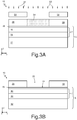
Figures 2-6 show, in a side section view, manufacturing steps for obtaining a HEMT device with ohmic contact recessed in a semiconductor body, according to an embodiment of the present invention; -
Figures 7-10 illustrate a variation of the manufacturing steps 3A-5; and -
Figure 11 illustrates a further variation of the manufacturing steps 3A-5. -
Figures 2-6 illustrate, in a side section view, in a triaxial cartesian reference system X, Y, Z, manufacturing steps for obtaining an ohmic-contact structure 10, of a recessed type, illustrated, as a whole, inFigure 6 . The structure 1 forms part of a HEMT device. - With reference to
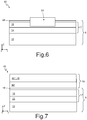
Figure 2 , asubstrate 12 of semiconductor material, such as silicon, or silicon carbide (SiC), or sapphire (Al2O3), or some other material, is provided. - Formed on the
substrate 12, in succession and in a way in itself known, along the direction of the axis Z are, respectively: a firststructural layer 14, in particular of intrinsic gallium nitride (GaN) (channel layer of the HEMT device), grown, for example epitaxially, on thesubstrate 12; a secondstructural layer 16, in particular of intrinsic aluminium and gallium nitride (AlGaN) or, more in general, of compounds based upon ternary or quaternary alloys of gallium nitride, such as AlxGa1-xN, AlInGaN, InxGa1-xN, AlxIn1-xAl (barrier layer of the HEMT device), grown, for example epitaxially, on thechannel layer 14; and optionally aprotection layer 18, in particular of GaN with a thickness of just a few nanometres (e.g., 1-4 nm), having the function of protecting thebarrier layer 16 from oxidation phenomena. - The
channel layer 14 and thebarrier layer 16 form, in a way in itself known, aheterostructure 17. - In a way not illustrated in the Figure, between the
substrate 12 and thechannel layer 14 one or more further buffer layers may be present, according to the need. - The
channel layer 14 has a thickness (along the axis Z), for example approximately between 1 µm and 5 µm; thebarrier layer 16 has a thickness (along the axis Z), for example approximately between 5 nm and 30 nm. - A
2DEG layer 15 is formed at the interface between thechannel layer 14 and thebarrier layer 16. The charge carriers belonging to the 2DEG are free to move in any direction in a plane XY (defined by the axes X and Y) at the2DEG interface 15, whereas they are confined along the axis Z. - The
substrate 12, thechannel layer 14, thebarrier layer 16, and theprotection layer 18 form asemiconductor body 5. - With reference to
Figure 3A , aphotoresist layer 28, with a thickness, for example, of between 1 and 3 µm is deposited. Saidphotoresist layer 28 entirely and evenly coats theepitaxial layer 18. - This is then followed by a step of photolithographic exposure (represented by the arrows 32) of the
photoresist layer 28, via the use of amask 30. The regions of thephotoresist layer 28 not covered by themask 30 thus become soluble during the subsequent etching step. - The
mask 30 is such that aregion 34 of thephotoresist layer 28 is exposed. Saidregion 34 defines the region in which the ohmic contact will be provided. - Then (
Figure 3B ), themask 30 is removed, and an etching step (e.g., of a wet type) is carried out for selective removal of theregion 34 of thephotoresist layer 28. Atrench 35 is thus formed in thephotoresist layer 28, through which asurface portion 19 of theprotection layer 18 is exposed. It may be noted that the process described with reference toFigures 1-3B does not require the deposition of a layer of passivating material (such as, for example, silicon nitride) as is typically envisaged in the prior art. - The photolithographic steps listed above have been described with reference to a positive photoresist. A different embodiment, not illustrated, envisages the use of a negative photoresist, as described with reference to
Figures 7-10 , or of a bi-layer. - With reference to
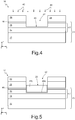
Figure 4 , an etch is then carried out (represented by arrows 40) for selective removal of portions of theprotection layer 18 and of theunderlying barrier layer 16, which are exposed through thetrench 35. More in particular, the etching process comprises a first step, for removing theprotection layer 18, and a second step, for partly or completely removing thebarrier layer 16. Both of these steps use a Cl2-based chemistry. - The
photoresist layer 28 functions as etching mask, for protecting the regions of thesemiconductor body 5 not exposed through thetrench 35. - At the
trench 35, thesemiconductor body 5 is then dug further, to form acontact trench 42, which extends in depth in thebarrier layer 16, terminating inside thebarrier layer 16 itself. Thecontact trench 42 is delimited underneath by abottom surface 44 of thebarrier layer 16. - The
contact trench 42 is adapted to house an ohmic contact, as described hereinafter. - With reference to the
etching process 40, the first etching step is designed to remove theprotection layer 18 throughout its entire thickness in the area exposed by thetrench 35, whereas the second etching step is designed to remove only part of the thickness, along Z, of thebarrier layer 16. It is evident that, in the absence of theprotection layer 18, which is optional, theetching process 40 comprises a single etching step for removing selective portions of thebarrier layer 16. - It is moreover evident that, in other embodiments, the
contact trench 42 may extend throughout the entire thickness of thebarrier layer 16, terminating at the interface with the underlying layer (here, the substrate 12), or else proceeding into the underlying layer, according to the design needs and parameters. - With reference to
Figure 5 , there then follows deposition of one or more layers of conductive material, in particular one or more metal layers, via known techniques, such as sputtering or evaporation. In particular, a stack of metal layers is formed (three of which are illustrated inFigures 5 and6 ) adapted to form anohmic contact 22. - Formation of the stack of metal layers comprises, according to one embodiment, forming a
first interface layer 22a and afilling layer 22b on theinterface layer 22a. Theinterface layer 22a is made of a material chosen from titanium or tantalum. Thefilling layer 22b is, in particular, made of aluminium. - Formation of the stack of metal layers comprises, according to a further embodiment, forming in succession a first titanium or tantalum layer, an aluminium layer, and a second layer, which is also made of titanium or tantalum. The Ti layer is adapted to promote the adhesion of the nickel or tungsten layer to the
bottom surface 44 of the contact trench 42 (i.e., to the barrier layer 16) and has the function ofinterface layer 22a. The Al layer functions, instead, as fillinglayer 22b, or central body, of theohmic contact 22. The last Ti or Ta layer serves as packaging layer. - It is evident that other materials, or a different number of layers, may be used to form the stack of the
ohmic contact 22, according to the design specifications. For instance, it is possible to omit theinterface layer 22a by depositing just thefilling layer 22b, which, in this case, is made of aluminium. - The one or more conductive materials for formation of the
ohmic contact 22 are both deposited inside thetrench 42 and on the outside thereof, over thephotoresist layer 28, which is thus covered at the top by aspurious metal deposition 45. - This is followed by a lift-off step, for removing both the
photoresist layer 28 and thespurious metal material 45. - A step of rapid thermal annealing (RTA) is then carried out, which enables perfecting of the ohmic contact, in a way in itself known. This procedure is conducted at a temperature ranging between approximately 450°C and approximately 650°C, in protected environment (for example, in a nitrogen or argon atmosphere).
-
Figure 6 shows thestructure 10 at the end of the manufacturing steps described, which includes the recessed gold-freeohmic contact 22. - As may be seen, the
ohmic contact 22 is automatically aligned, or self-aligned, to the recessed region formed previously in theheterostructure 17. - This result is achieved by using the
same photoresist layer 28 in two different steps of the manufacturing process. Firstly, thephotoresist layer 28 is used duringetching 40 as a mask for creation of the contact trench 42 (and hence for defining the recessed region in the heterostructure 17). Moreover, thephotoresist layer 28 is used as a further mask for forming theohmic contact 22, by deposition of metal material. - From an examination of the characteristics of the invention provided according to the present disclosure the advantages that it affords are evident.
- In particular it is possible to obtain gold-free ohmic contacts that present lower contact and access resistances, and the electrical performance of which is highly reproducible.
- The manufacturing process is simplified via the use of the photoresist layer as mask both during the etching step and during metal deposition of the ohmic contact. The ohmic contact is thus automatically aligned with the recessed AlGaN region. This enables better electrical performance to be achieved by the HEMT device and reduction of the related production costs, as well as guaranteeing structural quality of the ohmic contact.
- Having a low contact resistance enables a higher maximum current through the HEMT device, and hence a higher output power, to be obtained.
- A low contact resistance is moreover fundamental in radiofrequency applications for improving the frequency response of the HEMT device.
- According to the present invention, a passivation layer is not necessary for formation of the metal contact. The absence of passivating material in the process for manufacturing the ohmic contact enables a lower spread of the values of contact resistance to be obtained, thus improving the electrical properties of the HEMT device.
- The invention described herein hence reduces the costs for manufacturing the ohmic contacts, rendering the manufacturing process compatible with CMOS technology.
- Finally, it is clear that modifications and variations may be made to the invention described and illustrated herein, without thereby departing from the scope of protection thereof, as defined in the annexed claims.
- In particular, the steps of the formation of the trench through a
photoresist layer 28, of the deposition of theohmic contact 22, and the subsequent step of lift-off to remove both thephotoresist layer 28 and thespurious metal material 45, described with reference toFigures 3A-5 , can be replaced by the steps according toFigures 7-9 described hereinafter (structural elements, or process steps, found inFigures 3A-5 are not further described, and the same reference numbers will be used). - With reference to
Figure 7 , astack 60 of sacrificial layers is formed. In particular the following are formed: - a first sacrificial layer 60', of a non-photosensitive (or non-photoimageable) organic polymer solution, in particular, known commercially as "PMGI", or "SF11" (concerning a resist including a polydimethyl glutarimide polymer), with a thickness comprised between 0.6 µm and 1.3 µm (according to the subsequent thickness of metal that must be evaporated); and
- a second
sacrificial layer 60", of photosensitive or photoimageable material (i.e., photoresist), which extends over the first sacrificial layer 60', with a thickness comprised between 0.6 µm and 4 µm. - Both the first and second
sacrificial layers 60', 60" can be formed by spin-coating technique. - In the following, (
Figure 8 ), the secondsacrificial layer 60" is patterned, by a lithographic and development step, to remove selective portions of thesacrificial layer 60" at the region of thestructure 10 in which it is desired to form theohmic contact 22. Since the first sacrificial layer 60' is not photosensitive, the lithographic and development step of the secondsacrificial layer 60" has no effect on the first sacrificial layer 60'. At the end of the development of the secondsacrificial layer 60" (i.e., by TMAH), the first sacrificial layer 60' is partially exposed at the regions of the secondsacrificial layer 60" removed. During this step, also the isotropic etching of the first sacrificial layer 60' takes place, to uniformly remove the regions of the first sacrificial layer 60' exposed. Since the etching is of isotropic type, a removal of the first sacrificial layer 60' can also be seen below the secondsacrificial layer 60" (namely, an underetch or undercut phenomenon), that extends towards the source and drain regions, without reaching them. In the section view ofFigure 8 , undercutregions 65 extend, along the direction Y. - Following this step, the
stack 60 remains on thestructure 10, covering it, with the exception of regions where it is desired to form theohmic contact 22. - This is followed, (
Figure 9 ), by an etching (illustrated byarrows 68 inFigure 9 ) to remove selective portions of theprotection layer 18 and of theunderlying barrier layer 16, similarly to what is described with reference toFigure 4 . More in particular, the etching comprises a first step, to remove theprotection layer 18, and a second step, to partially or completely remove thebarrier layer 16. Both of the steps use a Cl2-based chemistry. The secondsacrificial layer 60" defines the etching mask, and in particular the exposed portions of theprotection layer 18 and of thebarrier layer 16 are removed through the opening defined in the step ofFigure 8 through the secondsacrificial layer 60". Thus forming a trench similar to thetrench 42 already described with reference toFigure 4 , and therefore illustrated herein with the same reference number. - In particular, it may be noted that the second
sacrificial layer 60" can correspond in terms of material, thickness and functional characteristics to thephotoresist layer 28 previously described. - Then, (Figure) 10, a step for the formation of the stack of metal layers which form the
ohmic contact 22 takes place, as described with reference toFigure 5 (comprising forming thefirst interface layer 22a and thefilling layer 22b), in particular through evaporation processes. Thesacrificial layer 60" is used as a deposition mask; thelayers - The one or more conductive materials for the formation of the
ohmic contact 22 are both deposited inside thetrench 42 and on the outside thereof, over the secondsacrificial layer 60", which is covered at the top by aspurious metal deposition 45. - Then, by a lift-off process of a per se known type, the first and the second
sacrificial layers 60', 60" are removed, together with thespurious metal deposition 45. The presence of the undercutregions 65 is advantageous during this lift-off step, since this conformation prevents the deposition of a uniform metal layer along the vertical walls of the first sacrificial layer 60', thus promoting the lift-off. - The
structure 10, illustrated inFigure 6 , is thus obtained. - In a further embodiment, the steps of
Figures 7-10 are carried out on a semiconductor body that does not have theprotection layer 18, therefore, thestack 60 is formed directly on thebarrier layer 16. - In a further embodiment, illustrated in
Figure 11 , thephotoresist layer 28 is formed with tilted side walls 28' (forming a structure of a truncated cone type with a larger base at the layer 18). The deposition, i.e., by evaporation, of one or more layers for forming theohmic contact 22, is typically carried out substantially along the vertical direction (axis Z). Consequently, the projection of the tilted side walls 28' would allow formation of theohmic contact 22 in thetrench 42 without having to be in direct contact with the tilted side walls 28' or the side walls of thelayers layers
Claims (9)
- A method for manufacturing an ohmic contact (22) for a HEMT device (1), comprising the steps of:- forming a sacrificial structure (28; 60) on a semiconductor body (5) comprising a heterostructure (17);- forming, through the sacrificial structure (28; 60), an opening (35; 42), through which a surface region (19) of the semiconductor body (5) is exposed at said heterostructure (17);- etching the surface region (19) of the semiconductor body (5) using said sacrificial structure (28; 60) as etching mask to form a trench (42) in the heterostructure (17);- depositing one or more metal layers (22a, 22b; 22) in said trench (42) and on the sacrificial structure (28; 60); and- carrying out a lift-off process of the sacrificial structure (28; 60).
- The method according to claim 1, wherein the sacrificial structure (28; 60) comprises a photoresist layer (28; 60"), and the step of depositing said one or more metal layers (22a, 22b; 22) comprises using the photoresist layer (28; 60") as deposition mask.
- The method according to claim 2, wherein the step of using the photoresist layer (28) as deposition mask comprises shaping the photoresist layer in order to form a through-opening through the photoresist layer, said through-opening being delimited by tilted side walls.
- The method according to any one of the preceding claims, wherein the step of forming the sacrificial structure (60) further comprises forming a sacrificial layer (60') of a non-photoimageable material below the photoresist layer (28; 60"),
and wherein the step of forming said opening (35; 42) comprises:carrying out a photolithographic process to remove selective portions of the photoresist layer (28; 60"), until reaching the first sacrificial layer (60'); andisotropically etching the first sacrificial layer (60') by forming an undercut region (65) between the photoresist layer (28; 60") and the semiconductor body (5). - The method according to claim 1 or claim 2, wherein the step of depositing said one or more metal layers comprises forming a stack including at least one metal interface layer (22a) in contact with said heterostructure (17) and at least one metal filling layer (22b) on the metal interface layer (22a).
- The method according to claim 5, wherein the step of forming the metal interface layer (22a) includes depositing a layer of a material chosen from titanium and tantalum; and the step of forming the metal filling layer (22b) includes depositing an aluminium layer.
- The method according to any one of the preceding claims, further comprising the step of carrying out a process of rapid thermal annealing (RTA) of said one or more metal layers.
- The method according to claim 7, wherein the RTA process is carried out at a temperature ranging between 450°C and 650°C.
- The method according to any one of the preceding claims, wherein the semiconductor body (5) comprises a substrate (12), a channel layer (14) on the substrate (12), and a barrier layer (16) on the channel layer (14),
said trench (42) being formed through part of the barrier layer (16) or throughout the thickness of the barrier layer.
Applications Claiming Priority (1)
| Application Number | Priority Date | Filing Date | Title |
|---|---|---|---|
| IT201800010656 | 2018-11-28 |
Publications (3)
| Publication Number | Publication Date |
|---|---|
| EP3660923A1 true EP3660923A1 (en) | 2020-06-03 |
| EP3660923B1 EP3660923B1 (en) | 2024-04-03 |
| EP3660923C0 EP3660923C0 (en) | 2024-04-03 |
Family
ID=65409416
Family Applications (1)
| Application Number | Title | Priority Date | Filing Date |
|---|---|---|---|
| EP19212334.7A Active EP3660923B1 (en) | 2018-11-28 | 2019-11-28 | Method for manufacturing an ohmic contact for a hemt device |
Country Status (3)
| Country | Link |
|---|---|
| US (2) | US12154967B2 (en) |
| EP (1) | EP3660923B1 (en) |
| CN (2) | CN211125660U (en) |
Cited By (2)
| Publication number | Priority date | Publication date | Assignee | Title |
|---|---|---|---|---|
| EP3836228A1 (en) | 2019-12-10 | 2021-06-16 | STMicroelectronics S.r.l. | Hemt transistor including field plate regions and manufacturing process thereof |
| EP4220687A1 (en) * | 2022-02-01 | 2023-08-02 | STMicroelectronics S.r.l. | Manufacturing process of an ohmic contact of a hemt device and hemt device |
Families Citing this family (4)
| Publication number | Priority date | Publication date | Assignee | Title |
|---|---|---|---|---|
| CN211125660U (en) * | 2018-11-28 | 2020-07-28 | 意法半导体股份有限公司 | Intermediate structure for fabricating high electron mobility transistor devices |
| US12194266B2 (en) | 2019-04-09 | 2025-01-14 | Becton, Dickinson And Company | Extension set to reduce extension tube kinking |
| KR102396072B1 (en) * | 2020-11-13 | 2022-05-11 | 한국원자력연구원 | Method for Forming the Ohmic Contact of GaN Based Electronic Device and the Ohmic Contact of GaN Based Electronic Device Formed by the Same |
| CN114420750A (en) * | 2021-11-30 | 2022-04-29 | 西安电子科技大学广州研究院 | Ohmic contact structure preparation method and device based on self-assembly mask technology |
Citations (2)
| Publication number | Priority date | Publication date | Assignee | Title |
|---|---|---|---|---|
| US20040094759A1 (en) | 2002-08-05 | 2004-05-20 | Hrl Laboratories, Llc | Process for fabricating ultra-low contact resistances in GaN-based devices |
| US20120205663A1 (en) | 2011-02-16 | 2012-08-16 | Fujitsu Limited | Semiconductor device, power-supply unit, amplifier and method of manufacturing semiconductor device |
Family Cites Families (9)
| Publication number | Priority date | Publication date | Assignee | Title |
|---|---|---|---|---|
| US5698900A (en) * | 1996-07-22 | 1997-12-16 | The United States Of America As Represented By The Secretary Of The Air Force | Field effect transistor device with single layer integrated metal and retained semiconductor masking |
| US7432536B2 (en) * | 2004-11-04 | 2008-10-07 | Cree, Inc. | LED with self aligned bond pad |
| TWI358091B (en) | 2008-05-20 | 2012-02-11 | Win Semiconductors Corp | A method of fabricating short-gate-length electrod |
| JP5531434B2 (en) * | 2009-03-31 | 2014-06-25 | 富士通株式会社 | Compound semiconductor device and manufacturing method thereof |
| CN103606516A (en) * | 2013-11-29 | 2014-02-26 | 中国科学院微电子研究所 | Low-temperature gold-free ohmic contact fabrication method for GaN-based high electron mobility transistors |
| US9761438B1 (en) * | 2014-05-08 | 2017-09-12 | Hrl Laboratories, Llc | Method for manufacturing a semiconductor structure having a passivated III-nitride layer |
| US9728444B2 (en) | 2015-12-31 | 2017-08-08 | International Business Machines Corporation | Reactive ion etching assisted lift-off processes for fabricating thick metallization patterns with tight pitch |
| CN107946358B (en) * | 2017-11-21 | 2025-01-24 | 华南理工大学 | An AlGaN/GaN heterojunction HEMT device compatible with Si-CMOS process and a manufacturing method thereof |
| CN211125660U (en) * | 2018-11-28 | 2020-07-28 | 意法半导体股份有限公司 | Intermediate structure for fabricating high electron mobility transistor devices |
-
2019
- 2019-11-26 CN CN201922065261.2U patent/CN211125660U/en active Active
- 2019-11-26 CN CN201911174700.1A patent/CN111243949A/en active Pending
- 2019-11-26 US US16/697,051 patent/US12154967B2/en active Active
- 2019-11-28 EP EP19212334.7A patent/EP3660923B1/en active Active
-
2024
- 2024-10-09 US US18/910,960 patent/US20250040164A1/en active Pending
Patent Citations (2)
| Publication number | Priority date | Publication date | Assignee | Title |
|---|---|---|---|---|
| US20040094759A1 (en) | 2002-08-05 | 2004-05-20 | Hrl Laboratories, Llc | Process for fabricating ultra-low contact resistances in GaN-based devices |
| US20120205663A1 (en) | 2011-02-16 | 2012-08-16 | Fujitsu Limited | Semiconductor device, power-supply unit, amplifier and method of manufacturing semiconductor device |
Non-Patent Citations (3)
| Title |
|---|
| FERDINANDO IUCOLANOGIUSEPPE GRECOFABRIZIO ROCCAFORTE, APPLIED PHYSICS LETTERS, vol. 103, 2013, pages 201604 |
| JING-NENG YAO ET AL.: "An Au-free GaN High Electron Mobility Transistor with Ti/Al/W Ohmic Metal Structure", 2015, IEEE |
| W. H. THAM ET AL.: "Al Ga - N/GaN MISHEMTs with a common gold-free metal-stack for source/drain/gate", IEEE ELECTRON DEVICE LETTERS, vol. 36, no. 12, December 2015 (2015-12-01), XP011590833, DOI: 10.1109/LED.2015.2491362 |
Cited By (2)
| Publication number | Priority date | Publication date | Assignee | Title |
|---|---|---|---|---|
| EP3836228A1 (en) | 2019-12-10 | 2021-06-16 | STMicroelectronics S.r.l. | Hemt transistor including field plate regions and manufacturing process thereof |
| EP4220687A1 (en) * | 2022-02-01 | 2023-08-02 | STMicroelectronics S.r.l. | Manufacturing process of an ohmic contact of a hemt device and hemt device |
Also Published As
| Publication number | Publication date |
|---|---|
| US20200168718A1 (en) | 2020-05-28 |
| CN111243949A (en) | 2020-06-05 |
| US12154967B2 (en) | 2024-11-26 |
| EP3660923B1 (en) | 2024-04-03 |
| EP3660923C0 (en) | 2024-04-03 |
| CN211125660U (en) | 2020-07-28 |
| US20250040164A1 (en) | 2025-01-30 |
Similar Documents
| Publication | Publication Date | Title |
|---|---|---|
| EP3660923B1 (en) | Method for manufacturing an ohmic contact for a hemt device | |
| JP5767637B2 (en) | Group III nitride semiconductor device and manufacturing method thereof | |
| US7897446B2 (en) | Method of forming a high electron mobility transistor hemt, utilizing self-aligned miniature field mitigating plate and protective dielectric layer | |
| KR101123459B1 (en) | Nitride-based transistors with a protective layer and a low-damage recess and methods of fabrication thereof | |
| CN107946358B (en) | An AlGaN/GaN heterojunction HEMT device compatible with Si-CMOS process and a manufacturing method thereof | |
| US20230246088A1 (en) | Manufacturing process of an ohmic contact of a hemt device and hemt device | |
| US12062715B2 (en) | HEMT transistor with adjusted gate-source distance, and manufacturing method thereof | |
| WO2021189182A1 (en) | Semiconductor device and manufacturing method therefor | |
| KR102261740B1 (en) | High frequency device and manufacturing method thereof | |
| US10134854B2 (en) | High electron mobility transistor and fabrication method thereof | |
| CN103390639A (en) | Group 13 nitride semiconductor device and method of its manufacture | |
| US20250095998A1 (en) | Method for manufacturing a gate terminal of a hemt device, and hemt device | |
| CN103000516B (en) | The method forming semiconductor structure | |
| US11211331B2 (en) | Semiconductor structure having a via and methods of manufacturing the same | |
| KR20090055593A (en) | Device comprising field effect heterostructure transistor and method for manufacturing same | |
| US12166101B2 (en) | High-electron-mobility transistor device and method of manufacturing the same | |
| JP5386810B2 (en) | MIS FET and manufacturing method thereof | |
| CN110581163A (en) | Semiconductor device and manufacturing method thereof |
Legal Events
| Date | Code | Title | Description |
|---|---|---|---|
| PUAI | Public reference made under article 153(3) epc to a published international application that has entered the european phase |
Free format text: ORIGINAL CODE: 0009012 |
|
| STAA | Information on the status of an ep patent application or granted ep patent |
Free format text: STATUS: THE APPLICATION HAS BEEN PUBLISHED |
|
| AK | Designated contracting states |
Kind code of ref document: A1 Designated state(s): AL AT BE BG CH CY CZ DE DK EE ES FI FR GB GR HR HU IE IS IT LI LT LU LV MC MK MT NL NO PL PT RO RS SE SI SK SM TR |
|
| AX | Request for extension of the european patent |
Extension state: BA ME |
|
| STAA | Information on the status of an ep patent application or granted ep patent |
Free format text: STATUS: REQUEST FOR EXAMINATION WAS MADE |
|
| 17P | Request for examination filed |
Effective date: 20201130 |
|
| RBV | Designated contracting states (corrected) |
Designated state(s): AL AT BE BG CH CY CZ DE DK EE ES FI FR GB GR HR HU IE IS IT LI LT LU LV MC MK MT NL NO PL PT RO RS SE SI SK SM TR |
|
| STAA | Information on the status of an ep patent application or granted ep patent |
Free format text: STATUS: EXAMINATION IS IN PROGRESS |
|
| 17Q | First examination report despatched |
Effective date: 20220406 |
|
| REG | Reference to a national code |
Ref country code: DE Ref legal event code: R079 Free format text: PREVIOUS MAIN CLASS: H01L0029450000 Ref country code: DE Ref legal event code: R079 Ref document number: 602019049371 Country of ref document: DE Free format text: PREVIOUS MAIN CLASS: H01L0029450000 Ipc: H01L0029400000 |
|
| GRAP | Despatch of communication of intention to grant a patent |
Free format text: ORIGINAL CODE: EPIDOSNIGR1 |
|
| STAA | Information on the status of an ep patent application or granted ep patent |
Free format text: STATUS: GRANT OF PATENT IS INTENDED |
|
| RIC1 | Information provided on ipc code assigned before grant |
Ipc: H01L 29/778 20060101ALN20231013BHEP Ipc: H01L 29/20 20060101ALN20231013BHEP Ipc: H01L 29/45 20060101ALI20231013BHEP Ipc: H01L 21/285 20060101ALI20231013BHEP Ipc: H01L 21/18 20060101ALI20231013BHEP Ipc: H01L 21/441 20060101ALI20231013BHEP Ipc: H01L 29/417 20060101ALI20231013BHEP Ipc: H01L 29/40 20060101AFI20231013BHEP |
|
| INTG | Intention to grant announced |
Effective date: 20231031 |
|
| GRAS | Grant fee paid |
Free format text: ORIGINAL CODE: EPIDOSNIGR3 |
|
| GRAA | (expected) grant |
Free format text: ORIGINAL CODE: 0009210 |
|
| STAA | Information on the status of an ep patent application or granted ep patent |
Free format text: STATUS: THE PATENT HAS BEEN GRANTED |
|
| AK | Designated contracting states |
Kind code of ref document: B1 Designated state(s): AL AT BE BG CH CY CZ DE DK EE ES FI FR GB GR HR HU IE IS IT LI LT LU LV MC MK MT NL NO PL PT RO RS SE SI SK SM TR |
|
| REG | Reference to a national code |
Ref country code: CH Ref legal event code: EP |
|
| REG | Reference to a national code |
Ref country code: DE Ref legal event code: R096 Ref document number: 602019049371 Country of ref document: DE |
|
| REG | Reference to a national code |
Ref country code: IE Ref legal event code: FG4D |
|
| U01 | Request for unitary effect filed |
Effective date: 20240408 |
|
| U07 | Unitary effect registered |
Designated state(s): AT BE BG DE DK EE FI FR IT LT LU LV MT NL PT SE SI Effective date: 20240416 |
|
| PG25 | Lapsed in a contracting state [announced via postgrant information from national office to epo] |
Ref country code: IS Free format text: LAPSE BECAUSE OF FAILURE TO SUBMIT A TRANSLATION OF THE DESCRIPTION OR TO PAY THE FEE WITHIN THE PRESCRIBED TIME-LIMIT Effective date: 20240803 |
|
| PG25 | Lapsed in a contracting state [announced via postgrant information from national office to epo] |
Ref country code: HR Free format text: LAPSE BECAUSE OF FAILURE TO SUBMIT A TRANSLATION OF THE DESCRIPTION OR TO PAY THE FEE WITHIN THE PRESCRIBED TIME-LIMIT Effective date: 20240403 |
|
| PG25 | Lapsed in a contracting state [announced via postgrant information from national office to epo] |
Ref country code: GR Free format text: LAPSE BECAUSE OF FAILURE TO SUBMIT A TRANSLATION OF THE DESCRIPTION OR TO PAY THE FEE WITHIN THE PRESCRIBED TIME-LIMIT Effective date: 20240704 |
|
| PG25 | Lapsed in a contracting state [announced via postgrant information from national office to epo] |
Ref country code: ES Free format text: LAPSE BECAUSE OF FAILURE TO SUBMIT A TRANSLATION OF THE DESCRIPTION OR TO PAY THE FEE WITHIN THE PRESCRIBED TIME-LIMIT Effective date: 20240403 |
|
| PG25 | Lapsed in a contracting state [announced via postgrant information from national office to epo] |
Ref country code: CZ Free format text: LAPSE BECAUSE OF FAILURE TO SUBMIT A TRANSLATION OF THE DESCRIPTION OR TO PAY THE FEE WITHIN THE PRESCRIBED TIME-LIMIT Effective date: 20240403 |
|
| PG25 | Lapsed in a contracting state [announced via postgrant information from national office to epo] |
Ref country code: PL Free format text: LAPSE BECAUSE OF FAILURE TO SUBMIT A TRANSLATION OF THE DESCRIPTION OR TO PAY THE FEE WITHIN THE PRESCRIBED TIME-LIMIT Effective date: 20240403 |
|
| PG25 | Lapsed in a contracting state [announced via postgrant information from national office to epo] |
Ref country code: PL Free format text: LAPSE BECAUSE OF FAILURE TO SUBMIT A TRANSLATION OF THE DESCRIPTION OR TO PAY THE FEE WITHIN THE PRESCRIBED TIME-LIMIT Effective date: 20240403 Ref country code: NO Free format text: LAPSE BECAUSE OF FAILURE TO SUBMIT A TRANSLATION OF THE DESCRIPTION OR TO PAY THE FEE WITHIN THE PRESCRIBED TIME-LIMIT Effective date: 20240703 Ref country code: IS Free format text: LAPSE BECAUSE OF FAILURE TO SUBMIT A TRANSLATION OF THE DESCRIPTION OR TO PAY THE FEE WITHIN THE PRESCRIBED TIME-LIMIT Effective date: 20240803 Ref country code: HR Free format text: LAPSE BECAUSE OF FAILURE TO SUBMIT A TRANSLATION OF THE DESCRIPTION OR TO PAY THE FEE WITHIN THE PRESCRIBED TIME-LIMIT Effective date: 20240403 Ref country code: GR Free format text: LAPSE BECAUSE OF FAILURE TO SUBMIT A TRANSLATION OF THE DESCRIPTION OR TO PAY THE FEE WITHIN THE PRESCRIBED TIME-LIMIT Effective date: 20240704 Ref country code: ES Free format text: LAPSE BECAUSE OF FAILURE TO SUBMIT A TRANSLATION OF THE DESCRIPTION OR TO PAY THE FEE WITHIN THE PRESCRIBED TIME-LIMIT Effective date: 20240403 Ref country code: CZ Free format text: LAPSE BECAUSE OF FAILURE TO SUBMIT A TRANSLATION OF THE DESCRIPTION OR TO PAY THE FEE WITHIN THE PRESCRIBED TIME-LIMIT Effective date: 20240403 Ref country code: RS Free format text: LAPSE BECAUSE OF FAILURE TO SUBMIT A TRANSLATION OF THE DESCRIPTION OR TO PAY THE FEE WITHIN THE PRESCRIBED TIME-LIMIT Effective date: 20240703 |
|
| U20 | Renewal fee for the european patent with unitary effect paid |
Year of fee payment: 6 Effective date: 20241022 |
|
| REG | Reference to a national code |
Ref country code: DE Ref legal event code: R097 Ref document number: 602019049371 Country of ref document: DE |
|
| PG25 | Lapsed in a contracting state [announced via postgrant information from national office to epo] |
Ref country code: RO Free format text: LAPSE BECAUSE OF FAILURE TO SUBMIT A TRANSLATION OF THE DESCRIPTION OR TO PAY THE FEE WITHIN THE PRESCRIBED TIME-LIMIT Effective date: 20240403 Ref country code: SK Free format text: LAPSE BECAUSE OF FAILURE TO SUBMIT A TRANSLATION OF THE DESCRIPTION OR TO PAY THE FEE WITHIN THE PRESCRIBED TIME-LIMIT Effective date: 20240403 |
|
| PG25 | Lapsed in a contracting state [announced via postgrant information from national office to epo] |
Ref country code: SM Free format text: LAPSE BECAUSE OF FAILURE TO SUBMIT A TRANSLATION OF THE DESCRIPTION OR TO PAY THE FEE WITHIN THE PRESCRIBED TIME-LIMIT Effective date: 20240403 |
|
| PG25 | Lapsed in a contracting state [announced via postgrant information from national office to epo] |
Ref country code: SM Free format text: LAPSE BECAUSE OF FAILURE TO SUBMIT A TRANSLATION OF THE DESCRIPTION OR TO PAY THE FEE WITHIN THE PRESCRIBED TIME-LIMIT Effective date: 20240403 Ref country code: SK Free format text: LAPSE BECAUSE OF FAILURE TO SUBMIT A TRANSLATION OF THE DESCRIPTION OR TO PAY THE FEE WITHIN THE PRESCRIBED TIME-LIMIT Effective date: 20240403 Ref country code: RO Free format text: LAPSE BECAUSE OF FAILURE TO SUBMIT A TRANSLATION OF THE DESCRIPTION OR TO PAY THE FEE WITHIN THE PRESCRIBED TIME-LIMIT Effective date: 20240403 |
|
| PLBE | No opposition filed within time limit |
Free format text: ORIGINAL CODE: 0009261 |
|
| STAA | Information on the status of an ep patent application or granted ep patent |
Free format text: STATUS: NO OPPOSITION FILED WITHIN TIME LIMIT |
|
| 26N | No opposition filed |
Effective date: 20250106 |
|
| REG | Reference to a national code |
Ref country code: CH Ref legal event code: PL |
|
| PG25 | Lapsed in a contracting state [announced via postgrant information from national office to epo] |
Ref country code: MC Free format text: LAPSE BECAUSE OF FAILURE TO SUBMIT A TRANSLATION OF THE DESCRIPTION OR TO PAY THE FEE WITHIN THE PRESCRIBED TIME-LIMIT Effective date: 20240403 |
|
| REG | Reference to a national code |
Ref country code: CH Ref legal event code: PL |
|
| GBPC | Gb: european patent ceased through non-payment of renewal fee |
Effective date: 20241128 |
|
| PG25 | Lapsed in a contracting state [announced via postgrant information from national office to epo] |
Ref country code: CH Free format text: LAPSE BECAUSE OF NON-PAYMENT OF DUE FEES Effective date: 20241130 |
|
| PG25 | Lapsed in a contracting state [announced via postgrant information from national office to epo] |
Ref country code: GB Free format text: LAPSE BECAUSE OF NON-PAYMENT OF DUE FEES Effective date: 20241128 |
|
| PG25 | Lapsed in a contracting state [announced via postgrant information from national office to epo] |
Ref country code: IE Free format text: LAPSE BECAUSE OF NON-PAYMENT OF DUE FEES Effective date: 20241128 |
|
| U20 | Renewal fee for the european patent with unitary effect paid |
Year of fee payment: 7 Effective date: 20251022 |
|
| PG25 | Lapsed in a contracting state [announced via postgrant information from national office to epo] |
Ref country code: HU Free format text: LAPSE BECAUSE OF FAILURE TO SUBMIT A TRANSLATION OF THE DESCRIPTION OR TO PAY THE FEE WITHIN THE PRESCRIBED TIME-LIMIT; INVALID AB INITIO Effective date: 20191128 |
|
| PG25 | Lapsed in a contracting state [announced via postgrant information from national office to epo] |
Ref country code: CY Free format text: LAPSE BECAUSE OF FAILURE TO SUBMIT A TRANSLATION OF THE DESCRIPTION OR TO PAY THE FEE WITHIN THE PRESCRIBED TIME-LIMIT; INVALID AB INITIO Effective date: 20191128 |