EP3660907A1 - Display device and manufacturing method thereof - Google Patents
Display device and manufacturing method thereof Download PDFInfo
- Publication number
- EP3660907A1 EP3660907A1 EP19204944.3A EP19204944A EP3660907A1 EP 3660907 A1 EP3660907 A1 EP 3660907A1 EP 19204944 A EP19204944 A EP 19204944A EP 3660907 A1 EP3660907 A1 EP 3660907A1
- Authority
- EP
- European Patent Office
- Prior art keywords
- layer
- light emitting
- partition wall
- display device
- auxiliary layer
- Prior art date
- Legal status (The legal status is an assumption and is not a legal conclusion. Google has not performed a legal analysis and makes no representation as to the accuracy of the status listed.)
- Granted
Links
Images





Classifications
-
- H—ELECTRICITY
- H10—SEMICONDUCTOR DEVICES; ELECTRIC SOLID-STATE DEVICES NOT OTHERWISE PROVIDED FOR
- H10K—ORGANIC ELECTRIC SOLID-STATE DEVICES
- H10K59/00—Integrated devices, or assemblies of multiple devices, comprising at least one organic light-emitting element covered by group H10K50/00
- H10K59/10—OLED displays
- H10K59/12—Active-matrix OLED [AMOLED] displays
-
- H—ELECTRICITY
- H10—SEMICONDUCTOR DEVICES; ELECTRIC SOLID-STATE DEVICES NOT OTHERWISE PROVIDED FOR
- H10K—ORGANIC ELECTRIC SOLID-STATE DEVICES
- H10K59/00—Integrated devices, or assemblies of multiple devices, comprising at least one organic light-emitting element covered by group H10K50/00
- H10K59/10—OLED displays
- H10K59/12—Active-matrix OLED [AMOLED] displays
- H10K59/122—Pixel-defining structures or layers, e.g. banks
-
- H—ELECTRICITY
- H10—SEMICONDUCTOR DEVICES; ELECTRIC SOLID-STATE DEVICES NOT OTHERWISE PROVIDED FOR
- H10K—ORGANIC ELECTRIC SOLID-STATE DEVICES
- H10K71/00—Manufacture or treatment specially adapted for the organic devices covered by this subclass
- H10K71/10—Deposition of organic active material
- H10K71/12—Deposition of organic active material using liquid deposition, e.g. spin coating
- H10K71/13—Deposition of organic active material using liquid deposition, e.g. spin coating using printing techniques, e.g. ink-jet printing or screen printing
- H10K71/135—Deposition of organic active material using liquid deposition, e.g. spin coating using printing techniques, e.g. ink-jet printing or screen printing using ink-jet printing
-
- H—ELECTRICITY
- H10—SEMICONDUCTOR DEVICES; ELECTRIC SOLID-STATE DEVICES NOT OTHERWISE PROVIDED FOR
- H10K—ORGANIC ELECTRIC SOLID-STATE DEVICES
- H10K2102/00—Constructional details relating to the organic devices covered by this subclass
- H10K2102/301—Details of OLEDs
- H10K2102/331—Nanoparticles used in non-emissive layers, e.g. in packaging layer
-
- H—ELECTRICITY
- H10—SEMICONDUCTOR DEVICES; ELECTRIC SOLID-STATE DEVICES NOT OTHERWISE PROVIDED FOR
- H10K—ORGANIC ELECTRIC SOLID-STATE DEVICES
- H10K2102/00—Constructional details relating to the organic devices covered by this subclass
- H10K2102/301—Details of OLEDs
- H10K2102/351—Thickness
-
- H—ELECTRICITY
- H10—SEMICONDUCTOR DEVICES; ELECTRIC SOLID-STATE DEVICES NOT OTHERWISE PROVIDED FOR
- H10K—ORGANIC ELECTRIC SOLID-STATE DEVICES
- H10K59/00—Integrated devices, or assemblies of multiple devices, comprising at least one organic light-emitting element covered by group H10K50/00
- H10K59/10—OLED displays
- H10K59/12—Active-matrix OLED [AMOLED] displays
- H10K59/1201—Manufacture or treatment
-
- H—ELECTRICITY
- H10—SEMICONDUCTOR DEVICES; ELECTRIC SOLID-STATE DEVICES NOT OTHERWISE PROVIDED FOR
- H10K—ORGANIC ELECTRIC SOLID-STATE DEVICES
- H10K59/00—Integrated devices, or assemblies of multiple devices, comprising at least one organic light-emitting element covered by group H10K50/00
- H10K59/30—Devices specially adapted for multicolour light emission
- H10K59/38—Devices specially adapted for multicolour light emission comprising colour filters or colour changing media [CCM]
-
- H—ELECTRICITY
- H10—SEMICONDUCTOR DEVICES; ELECTRIC SOLID-STATE DEVICES NOT OTHERWISE PROVIDED FOR
- H10K—ORGANIC ELECTRIC SOLID-STATE DEVICES
- H10K71/00—Manufacture or treatment specially adapted for the organic devices covered by this subclass
- H10K71/10—Deposition of organic active material
- H10K71/12—Deposition of organic active material using liquid deposition, e.g. spin coating
-
- H—ELECTRICITY
- H10—SEMICONDUCTOR DEVICES; ELECTRIC SOLID-STATE DEVICES NOT OTHERWISE PROVIDED FOR
- H10K—ORGANIC ELECTRIC SOLID-STATE DEVICES
- H10K71/00—Manufacture or treatment specially adapted for the organic devices covered by this subclass
- H10K71/10—Deposition of organic active material
- H10K71/12—Deposition of organic active material using liquid deposition, e.g. spin coating
- H10K71/13—Deposition of organic active material using liquid deposition, e.g. spin coating using printing techniques, e.g. ink-jet printing or screen printing
Definitions
- the present disclosure relates to a display device and a manufacturing method thereof.
- a light emitting display device includes two electrodes and a light emitting layer disposed therebetween. An electron injected from one electrode that serves as a cathode, and a hole injected from the other electrode which serves as an anode are coupled with each other in the light emitting layer to generate an exciton. The exciton emits energy to emit light.
- the light emitting display device includes a plurality of pixels having a light emitting diode including a cathode, an anode, and a light emitting layer, and each pixel includes a plurality of transistors and capacitors for driving the light emitting diode.
- Exemplary embodiments provide a display device and a manufacturing method thereof that may stably include a light emitting layer formed by a solution process by providing an auxiliary layer that is effectively formed while providing lyophobicity on a partition wall.
- An exemplary embodiment provides a display device including a partition wall disposed on a substrate between a first electrode and a second electrode.
- the partition wall has an opening.
- a light emitting layer is disposed in the opening.
- An auxiliary layer having lyophobicity is disposed between the partition wall and the second electrode.
- a maximum thickness of the auxiliary layer may be about 100 nm or more and about 200 nm or less.
- a maximum thickness of the partition wall may be about 1 ⁇ m or more and about 1.5 ⁇ m or less.
- the auxiliary layer may not overlap the opening.
- the auxiliary layer may include at least one of a fluorine-based compound and a siloxane-based compound.
- the fluorine-based compound may be represented by Chemical Formula 1
- the siloxane-based compound may be represented by Chemical Formula 2.
- a lateral edge of the auxiliary layer is inclined and is aligned with an inclined lateral edge of the partition wall.
- the auxiliary layer may expose a portion of an upper surface of the partition wall.
- the auxiliary layer may overlap a lateral surface of the partition wall.
- the light emitting layer may include a quantum dot.
- the display device may further include a red color converting layer, a green color converting layer, and a transmissive layer that overlaps the light emission layer.
- Each of the red color converting layer and the green color converting layer may include a quantum dot.
- a display device including a partition wall disposed on a substrate between a first electrode and a second electrode.
- the partition wall has an opening.
- a light emitting layer is disposed in the opening.
- An auxiliary layer is disposed between the partition wall and the second electrode.
- the auxiliary layer includes a plurality of nanoparticles, and a surface of the auxiliary layer facing the second electrode is provided with protrusions and depressions.
- a thickness of the auxiliary layer may be about 30 nm to about 200 nm.
- the plurality of nanoparticles may include silica nanoparticles.
- Another exemplary embodiment provides a manufacturing method of a display device, including forming a thin film transistor and a pixel electrode connected to the thin film transistor on a substrate.
- a first material layer is formed overlapping the pixel electrode on the substrate.
- the first material layer is etched to form a partition wall including an opening.
- a residual film that is formed on the pixel electrode is removed.
- An auxiliary layer is formed having lyophobicity on the partition wall.
- the removing of the residual film may use at least one of a plasma process and a UVO 3 process.
- the forming of the auxiliary layer may include forming a second material layer on the partition wall, and removing an uncured area in the second material layer, and the removing of the uncured area may use an organic solvent.
- the organic solvent may include at least one of toluene, cyclopentanone, anisole, and propylene glycol methyl ether acetate (PGMEA).
- PGMEA propylene glycol methyl ether acetate
- the second material layer may include the same solvent as the organic solvent.
- the manufacturing method of the display device may further include providing a light emitting solution on the opening, and drying the light emitting solution to form a light emitting layer.
- Another exemplary embodiment provides a manufacturing method of a display device, including forming a thin film transistor and a pixel electrode connected to the thin film transistor on a substrate.
- a first material layer and a second material layer are sequentially formed overlapping the substrate on the pixel electrode.
- the first material layer and the second material layer are etched to form a partition wall having an opening and an auxiliary layer.
- a residual film formed on the pixel electrode is removed.
- the second material layer may include a plurality of nanoparticles.
- a light emitting layer through a solution process by including an auxiliary layer that is stably formed on an upper surface of a partition wall and has lyophobicity. Reliability of a light emitting diode and a display device including such a light emitting layer may be improved.
- the phrase “on a plane” means viewing a target portion from the top
- the phrase “on a cross-section” means viewing a cross-section formed by vertically cutting a target portion from the side.
- FIG. 1 illustrates a cross-sectional view of a display device according to an exemplary embodiment of the present inventive concepts.
- a substrate 110 may include a transparent glass substrate.
- the substrate 110 may include a plastic layer and a barrier layer that are alternately stacked.
- the substrate 110 according to an exemplary embodiment may be a flexible substrate which may be bent, folded, rolled, etc.
- a buffer layer 111 is disposed on the substrate 110.
- the buffer layer 111 may prevent impurities or the like from diffusing from the substrate 110 toward the inside of the display device.
- the buffer layer 111 may improve a flatness of a surface of the substrate 110 (e.g., planarize the surface of the substrate) in embodiments in which the surface of the substrate 110 is not uniform.
- the buffer layer 111 may include an inorganic insulating material such as a silicon oxide, a silicon nitride, or the like. However, in some exemplary embodiments, the buffer layer 111 may include an organic insulating material.
- the buffer layer 111 may be a single layer or have a multilayer structure. For example, in an exemplary embodiment in which the buffer layer 111 is a dual layer, a lower layer thereof may include a silicon nitride and an upper layer thereof may include a silicon oxide. However, exemplary embodiments of the present inventive concepts are not limited thereto.
- a semiconductor layer 130 is disposed on the buffer layer 111.
- the semiconductor layer 130 may include amorphous silicon, polycrystalline silicon, an oxide semiconductor, and the like.
- exemplary embodiments of the present inventive concepts are not limited thereto.
- the semiconductor layer 130 may include a source region 132 connected to a source electrode 153, a drain region 133 connected to a drain electrode 155, and a channel region 131 disposed between the source region 132 and the drain region 133, which will be described later.
- the source region 132 and the drain region 133 may be doped with an impurity.
- a first insulating film 141 is disposed on the semiconductor layer 130 and the buffer layer 111.
- the first insulating film 141 may be disposed directly on upper surfaces (e.g., in the second direction D2) of the semiconductor layer 130 and buffer layer 111.
- the first insulating film 141 may include an inorganic insulating material such as a silicon nitride, a silicon oxide, a metal oxide, or the like.
- the first insulating film 141 may include an organic insulating material.
- a gate electrode 124 is disposed on the first insulating film 141.
- the gate electrode 124 may be disposed directly on an upper surface (e.g., in the second direction D2) of the first insulating film 141.
- the gate electrode 124 overlaps (e.g., in the second direction D2) the channel region 131 of the semiconductor layer 130.
- the gate electrode 124 may include at least one material selected from aluminum (Al), platinum (Pt), palladium (Pd), silver (Ag), magnesium (Mg), gold (Au), nickel (Ni), neodymium (Nd), iridium (Ir), chromium (Cr), lithium (Li), calcium (Ca), molybdenum (Mo), titanium (Ti), tungsten (W), and copper (Cu).
- the gate electrode 124 may include a single layer or a multilayer structure.
- a second insulating film 142 may be disposed on the gate electrode 124 and the first insulating film 141.
- the second insulating film 142 may be disposed directly on an upper surface (e.g., in the second direction D2) of the first insulating film 141.
- the second insulating film 142 may include an inorganic insulating material such as a silicon nitride, a silicon oxide or the like.
- the second insulating film 142 may include an organic insulating material.
- the source electrode 153 and the drain electrode 155 may be disposed on the second insulating film 142.
- the source electrode 153 and the drain electrode 155 may be disposed directly on an upper surface (e.g., in the second direction D2) of the second insulating film 142.
- the source electrode 153 and the gate electrode 155 may include at least one material selected from aluminum (Al), platinum (Pt), palladium (Pd), silver (Ag), magnesium (Mg), gold (Au), nickel (Ni), neodymium (Nd), iridium (Ir), chromium (Cr), lithium (Li), calcium (Ca), molybdenum (Mo), titanium (Ti), tungsten (W), and copper (Cu).
- the source electrode 153 and the drain electrode 155 may include a single layer or a multilayer structure.
- the source electrode 153 and the drain electrode 155 may be connected to the source region 132 and the drain region 133 of the semiconductor layer 130, respectively, through contact holes formed in the first insulating film 141 and the second insulating film 142.
- a third insulating film 160 is disposed on the source electrode 153 and the drain electrode 155.
- the third insulating film 160 may cover the source electrode 153 and the drain electrode 155 for planarization thereof.
- the third insulating film 160 may include an organic insulating material or an inorganic insulating material.
- the first electrode which is a pixel electrode 191 is disposed on the third insulating film 160.
- the pixel electrode 191 may be disposed directly on an upper surface (e.g., in the second direction D2) of the third insulating film 160.
- the pixel electrode 191 may be connected to the drain electrode 155 through a contact hole formed in the third insulating film 160.
- the pixel electrode 191 may be a transparent electrode, a transflective electrode, or a reflective electrode.
- the pixel electrode 191 may be formed of ITO, IZO, ZnO, In 2 O 3 , IGO, or AZO.
- the pixel electrode 191 may include a reflective film including Ag, Mg, Al, Pt, Pd, Au, Ni, Nd, Ir, Cr, and a compound thereof, and a layer including ITO, IZO, ZnO, In 2 O 3 , IGO, or AZO.
- exemplary embodiments of the pixel electrode 191 are not limited thereto, and the pixel electrode 191 may include various materials, and may have variously modified structures such as a single layer structure or a multi-layer structure.
- a partition wall 360 is disposed on the pixel electrode 191 and the third insulating film 160.
- the partition wall 360 may be disposed directly on an upper surface (e.g., in the second direction D2) and lateral edge surfaces of the pixel electrode 191 and an upper surface of the third insulating film 160.
- the partition wall 360 includes an opening 365 that exposes a portion of the pixel electrode 191.
- a light emitting layer 370 may be disposed in the opening 365.
- the light emitting layer 370 may be disposed directly on the portion of the pixel electrode 191 exposed by the opening 365.
- An exposed region of the pixel electrode 191 having the light emitting layer thereon may be a light emitting region and a region in which the partition wall 360 covers the pixel electrode may be a non-light emitting region.
- the partition wall 360 may be a pixel defining layer.
- the partition wall 360 may be lyophilic. In a process in which a light emitting solution is provided in the opening 365, the light emitting solution may be stably injected into the opening, adjacent to the lyophilic partition wall 360. The lyophilic partition wall 360 may help stably position the light emitting solution within the opening 365.
- the partition wall 360 may include an organic material.
- the organic material may be benzocyclobutene, a polyamide resin, a polyacrylic resin, a polyimide resin, a phenol resin, or a siloxane-based inorganic material.
- exemplary embodiments of the present inventive concepts are not limited thereto.
- the partition wall 360 may additionally include at least one of an initiator, a crosslinking agent, a photoactive agent, and a surfactant.
- the partition wall 360 may include a photoactive agent when it includes a positive photoresist, and the partition wall 360 may include an initiator when it includes a negative photoresist.
- a maximum thickness t1 of the partition wall 360 (e.g., the length from a top surface of the partition wall to a bottom surface of the partition wall in the second direction D2) may be about 1 ⁇ m to about 1.5 ⁇ m.
- Lateral edges of the partition wall 360 forming the opening may have a tapered shape toward the substrate 110.
- the opening 365 may expose lateral edges of the partition wall 360 which are spaced farther apart as the distance from the substrate increases.
- the thickness t1 of the partition wall 360 in the flat region which does not include the inclined lateral edges of the partition wall may be about 1 ⁇ m to about 1.5 ⁇ m.
- the thickness of the partition wall 360 is less than about 1 ⁇ m, a distinction between a light emitting region in which the light emitting layer is disposed and a non-light emitting region in which a light emitting layer is not disposed is not clear and a resolution of the display device may be lowered.
- the thickness of the partition wall 360 is greater than about 1.5 ⁇ m, it is difficult for other components that are stacked on the partition 360 to have a uniform profile in a continuous shape.
- the light emitting layer 370 is disposed on the pixel electrode 191 exposed by the opening 365 as described above.
- a common electrode 270 is disposed on the light emitting layer 370 and the partition wall 360.
- the common electrode 270 may be disposed directly on an upper surface (e.g., in the second direction D2) of the light emitting layer 370 and the partition wall 360.
- the pixel electrode 191, the light emitting layer 370, and the common electrode 270 may form a light emitting diode.
- the common electrode 270 may be a transparent electrode, a transflective electrode, or a reflective electrode.
- the common electrode 270 may include a layer including a metal having a small work function, such as Li, Ca, LiF/Ca, LiF/Al, Al, Ag, Mg, and a compound thereof, and a transparent layer such as ITO, IZO, ZnO, or In 2 O 3 , or a transflective conductive layer.
- the common electrode 270 is a reflective electrode, it may include, for example, a layer including Li, Ca, LiF/Ca, LiF/Al, Al, Ag, Mg, and a compound thereof.
- the materials and the stacked structure of the common electrode 270 are not limited thereto, and exemplary embodiments of the present inventive concepts may have various modifications and arrangements.
- the pixel electrode 191 is an anode that is a hole injection electrode
- the common electrode 270 is a cathode that is an electron injection electrode.
- exemplary embodiments of the present inventive concepts are not limited thereto.
- the pixel electrode 191 may be a cathode and the common electrode 270 may be an anode according to a driving method of the display device. Holes and electrons are injected into the light emitting layer 370 from the pixel electrode 191 and the common electrode 270, respectively, and exitons generated by coupling the injected holes and electrons fall from an excited state to a ground state to emit light.
- the light emitting layer 370 may include a low molecular organic material or a polymer organic material such as poly(3,4-ethylenedioxythiophene) (PEDOT).
- the light emitting layer 370 may include a multilayer structure that includes a light emitting layer and at least one of a hole injecting layer, a hole transporting layer, an electron transporting layer, and an electron injecting layer. In embodiments in which all of these layers are included, the hole injecting layer is disposed on the pixel electrode 191, which is an anode, and the hole transporting layer, the light emitting layer, the electron transporting layer, and an electron injecting layer may be sequentially stacked thereon.
- the light emitting layer 370 may include a quantum dot.
- the quantum dot may emit red light, green light, or blue light.
- a core of the quantum dot may be selected from Group II-VI compounds, Group III-V compounds, Group IV-VI compounds, Group IV elements, Group IV compounds, and combinations thereof.
- the Group II-VI compound may be selected from: a two-element compound selected from CdSe, CdTe, ZnS, ZnSe, ZnTe, ZnO, HgS, HgSe, HgTe, MgSe, MgS, and a mixture thereof; a three-element compound selected from CdSeS, CdSeTe, CdSTe, ZnSeS, ZnSeTe, ZnSTe, HgSeS, HgSeTe, HgSTe, CdZnS, CdZnSe, CdZnTe, CdHgS, CdHgSe, CdHgTe, HgZnS, HgZnSe, HgZnTe, MgZnSe, MgZnS, and a mixture thereof; and a four-element compound selected from HgZnTeS, CdZnSeS, CdZnSeTe,
- the Group III-V compound may be selected from: a two-element compound selected from GaN, GaP, GaAs, GaSb, AlN, AlP, AlAs, AlSb, InN, InP, InAs, InSb, and a mixture thereof; a three-element compound selected from GaNP, GaNAs, GaNSb, GaPAs, GaPSb, AlNP, AlNAs, AlNSb, AlPAs, AlPSb, InGaP, InNP, InNAs, InNSb, InPAs, InPSb, GaAlNP, and a mixture thereof; and a four-element compound selected from GaAlNAs, GaAlNSb, GaAlPAs, GaAlPSb, GaInNP, GaInNAs, GaInNSb, GaInPAs, GaInPSb, InAlNP, InAlNAs, InAlNSb, InAlPAs, InAlPSb, and a mixture thereof.
- the Group IV-VI compound may be selected from: a two-element compound selected from SnS, SnSe, SnTe, PbS, PbSe, PbTe, and a mixture thereof; a three-element compound selected from SnSeS, SnSeTe, SnSTe, PbSeS, PbSeTe, PbSTe, SnPbS, SnPbSe, SnPbTe, and a mixture thereof; and a four-element compound selected from SnPbSSe, SnPbSeTe, SnPbSTe, and a mixture thereof.
- the Group IV element may be selected from Si, Ge, and a mixture thereof.
- the Group IV compound may be a two-element compound selected from SiC, SiGe, and a mixture thereof.
- the two-element compound, the three-element compound, or the four-element compound may be present in particles of the quantum dots at uniform concentrations, or they may be divided into states having partially different concentrations to be present in the same particle, respectively.
- a core/shell structure in which some quantum dots enclose some other quantum dots may be possible.
- an interface between the core and the shell may have a concentration gradient in which a concentration of elements of the shell decreases as the distance to the shell center decreases.
- the quantum dot may have a core-shell structure that includes a core including the nanocrystal described above and a shell surrounding the core.
- the shell of the quantum dot may serve as a passivation layer for maintaining a semiconductor characteristic and/or as a charging layer for applying an electrophoretic characteristic to the quantum dot by preventing chemical denaturation of the core.
- the shell may be a single layer or have a multilayer structure.
- An example of the shell of the quantum dot includes a metal or nonmetal oxide, a semiconductor compound, or a combination thereof.
- the metal or nonmetal oxide may be a two-element compound such as SiO 2 , Al 2 O 3 , TiO 2 , ZnO, MnO, Mn 2 O 3 , Mn 3 O 4 , CuO, FeO, Fe 2 O 3 , Fe 3 O 4 , CoO, Co 3 O 4 , NiO, and the like, or a three-element compound such as MgAl 2 O 4 , CoFe 2 O 4 , NiFe 2 O 4 , CoMn 2 O 4 , and the like.
- exemplary embodiments of the present inventive concepts are not limited thereto.
- the semiconductor compound may be CdS, CdSe, CdTe, ZnS, ZnSe, ZnTe, ZnSeS, ZnTeS, GaAs, GaP, GaSb, HgS, HgSe, HgTe, InAs, InP, InGaP, InSb, AlAs, AlP, AlSb, or the like.
- exemplary embodiments of the present inventive concepts are not limited thereto.
- the quantum dot may have a full width at half maximum (FWHM) of the light-emitting wavelength spectrum that is equal to or less than about 45 nm.
- FWHM full width at half maximum
- the quantum dot may have a FWHM equal to or less than about 40 nm.
- the quantum dot may have a FWHM equal to or less than about 30 nm. In this range, color purity or color reproducibility of the display device may be improved.
- a viewing angle of the transmitted light may be improved.
- a shape of the quantum dot is not particularly limited in embodiments and may include a spherical, pyramidal, multi-arm, or cubic nanoparticle, nanotube, nano-wire, nano-fiber, nano-plate particle shape, and the like.
- the quantum dot may control a color of emitted light according to a particle size thereof. Therefore, the quantum dot may have various light emitting colors such as blue, red, and green colors.
- the light emitting layer 370 may be formed by a solution process.
- the light emitting layer 370 may be formed by using any one of the following processes: spin coating, inkjet printing, gravure printing, roll-to-roll printing, syringe injection, dip coating, spray coating, relief printing, and screen printing.
- an auxiliary layer 380 is disposed between the common electrode 270 and the partition wall 360.
- the auxiliary layer 380 may be disposed on an upper surface of the partition wall 360.
- a lower surface (e.g., in the second direction D2) of the auxiliary layer 380 may be disposed directly on an upper surface of the partition wall 360 and an upper surface of the auxiliary layer 380 may contact a lower surface of the common electrode 270.
- the auxiliary layer 380 may not overlap the opening 365 of the partition wall 360 in the second direction D2.
- the auxiliary layer 380 may not overlap lateral edge surfaces of the partition wall 360 in the second direction D2.
- the auxiliary layer 380 may be generally spaced apart in the first direction D1 from the opening 365 of the partition wall. However, as described in more detail later, in an exemplary embodiment, the lower surface of the lateral edge of the auxiliary layer may substantially overlap (e.g., in the second direction D2) the upper surface of the lateral edge of the partition wall.
- the auxiliary layer 380 may have lyophobicity.
- the auxiliary layer 380 may include a composition having lyophobicity.
- a light emitting solution for forming the light emitting layer 370 may contact the auxiliary layer 380.
- the light emitting solution e.g. solvent for the light emitting layer
- the auxiliary layer 380 may repel the light emitting solution.
- the light emitting solution may be positioned in the opening 365 without contacting the auxiliary layer 380, and particularly, it may form a stable light emitting layer 370 that does not flow over from the opening 365. Therefore, the reliability of the light emitting diode including the light emitting layer 370 and the display device may thereby be improved.
- the lyophobicity means a property of pushing out a solution and not allowing the solution to penetrate well (i.e. "solvent rejecting")
- the word "lyophilic” means a property of having an affinity for a solution (i.e. "solvent preferring”).
- a solution may have a low surface bonding force with one surface having a lyophobic property and may have an excellent surface bonding force with another surface being lyophilic. Therefore, according to exemplary embodiments of the present inventive concepts, the surface bonding force between the light emitting solution and the auxiliary layer 380 may be weaker than the surface bonding force between the light emitting solution and the partition wall 360.
- a contact angle of the light emitting solution with respect to the auxiliary layer 380 may be, for example, about 40 degrees or more.
- the auxiliary layer 380 may include a material that is lyophobic to the light emitting solution.
- the auxiliary layer 380 may include a monomer or polymer.
- the auxiliary layer 380 may include a fluorine-based compound or a siloxane-based compound.
- the auxiliary layer 380 may include any compound having lyophobicity.
- the fluorine-based compound may be represented by Chemical Formula 1
- the siloxane-based compound may be represented by Chemical Formula 2.
- exemplary embodiments of the present inventive concepts are not limited thereto.
- a maximum thickness t2 of the auxiliary layer 380 may be about 100 nm to about 200 nm or less.
- the maximum thickness t2 of the auxiliary layer 380 may be between about 120 nm to about 180 nm or less.
- the maximum thickness t1 of the partition wall 360 is about 1 ⁇ m to about 1.5 ⁇ m, the auxiliary layer 380 is considerably thinner than the partition wall.
- the auxiliary layer 380 may be formed to be a thin layer for providing lyophobicity to the upper surface of the partition wall 360.
- the thickness of the auxiliary layer 380 is less than 100 nm, it may be difficult to substantially form a layer that has lyophobicity.
- the thickness of the auxiliary layer 380 may not exceed 200 nm so that the auxiliary layer 380 is sufficiently lyophobic and the light emitting solution forming the light emitting layer 370 is stably positioned on the opening 365.
- the thickness of the auxiliary layer 380 exceeds 200 nm, the light emitting solution injected into the opening 365 may be excessively swollen, and the light emitting solution may flow into an adjacent opening for mixture with the contents therein and may not be stably positioned in the opening.
- the auxiliary layer 380 may have surface energy of about 15 dyne/cm or less
- the light emitting solution for forming the light emitting layer 370 may have surface energy of about 17 to 35 dyne/cm
- the pixel electrode 191 may have surface energy of about 40 dyne/cm.
- the partition wall 360 may have surface energy of about 30 dyne/cm to about 43 dyne/cm.
- the surface energy of the partition wall 360 may be greater than the surface energies of the light emitting layer 370 and the auxiliary layer 380, and may be smaller than the surface energy of the pixel electrode 191.
- the auxiliary layer 380 is disposed on the partition wall 360, and may form a separate layer from the partition wall 360. Since the auxiliary layer 380 is formed through a separate manufacturing process from that of the partition wall 360, an interface may be formed between the partition wall 360 and the auxiliary layer 380.
- the lateral edge 381 of the auxiliary layer 380 may inclined so that is substantially aligned with the inclined lateral edge of the partition wall 360.
- the lower surface of the lateral edge 381 of the auxiliary layer 380 and the upper surface of the lateral edge of the partition wall 360 may substantially overlap (e.g., in the second direction D2).
- the auxiliary layer 380 may be manufactured by using a same mask as a mask used for forming the partition wall 360 in a manufacturing process.
- the light emitting solution is not positioned on an upper surface of the lyophobic auxiliary layer 380 and may be stably provided in the opening 365 included in the partition wall 360.
- the lyophobic auxiliary layer 380 prevents the light emitting solution from overflowing the partition wall 360. Therefore, the light emitting layer 370 may have improved reliability, and a light emitting diode and a display device with improved reliability may be provided.
- An encapsulation layer 400 for protecting the light emitting diode may be disposed on the common electrode 270.
- the encapsulation layer 400 may be disposed directly on an upper surface (e.g., in the second direction D2) of the common electrode 270.
- the encapsulation layer 400 may be sealed to the substrate 110 by a sealant.
- the encapsulation layer 400 may be formed of various materials such as glass, quartz, ceramic, plastic, metal and combinations thereof.
- the encapsulation layer 400 may be disposed on the common electrode 270 without using a sealant.
- the encapsulation layer 400 may include a single layer of an inorganic film or a single layer of an organic film.
- the encapsulation layer 400 may also include a multilayer structure in which an inorganic film and an organic film are alternately stacked.
- the encapsulation layer 400 may include two inorganic films, and an organic film disposed between the two inorganic films.
- a pixel may be a minimum unit for displaying an image.
- the thin film transistor is disposed at each pixel in the display area and the light emitting diode is connected to the thin film transistor.
- one pixel may include at least two thin film transistors and one capacitor.
- exemplary embodiments of the present inventive concepts are not limited thereto.
- one pixel may include three or more thin film transistors and two or more capacitors.
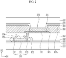
- FIG. 2 illustrates a cross-sectional view of a display device according to an exemplary embodiment.
- FIG. 3 illustrates a cross-sectional view of a display device according to an exemplary embodiment.
- FIG. 4 illustrates a cross-sectional view of a display device according to an exemplary embodiment. A description of the same constituent elements as those of the exemplary embodiment described above will be omitted.
- the auxiliary layer 380 may be disposed between the partition wall 360 and the common electrode 270.
- the auxiliary layer 380 may be disposed only on the upper surface of the partition wall 360, and the lower surface of the lateral edge of the auxiliary layer may not substantially overlap the upper surface of the inclined lateral edges of the partition wall 360.
- the lateral edge 381 of the auxiliary layer 380 may terminate in the first direction D1 prior to reaching a portion that overlaps the inclined lateral edge of the partition wall in the second direction D2.
- the auxiliary layer 380 may expose a portion of an upper surface 360s of the partition wall 360 from the lateral edge of the partition wall to a portion overlapping the lateral edge of the auxiliary layer in the second direction D2.
- the common electrode 270 may overlap the portion of the upper surface 360s of the partition wall 360 exposed by the auxiliary layer 380 in the second direction D2.
- the upper and lower portions of the lateral edge 381 of the auxiliary layer 380 may overlap not only the upper surface of the partition wall 360, but also portions of the lateral edge below the upper surface of the partition wall 360.
- the lateral edge 381 of the auxiliary layer may extend past the edge of the upper surface of the partition wall 360 in the first direction D1 and may overlap with the light emitting layer 370 in the second direction D2.
- the lateral edge 381 of the auxiliary layer may extend downward in the second direction D2 and may cover upper portions of the lateral edge of the partition wall 360.
- the lateral edge has a semicircular shape for the portion that extends past the lateral edge of the upper surface of the partition wall in the first direction D1 towards regions overlapping the light emitting layer 381 in the second direction D2.
- this portion of the lateral edge may have a variety of different shapes.
- the auxiliary layer 380 may provide lyophobicity not only to the upper surface of the partition wall 360 but also to an upper end of the lateral surface of the partition wall 360. Therefore, when the light emitting solution is injected into the opening 365, sufficient lyophobicity by the auxiliary layer 380 may be provided, particularly in a region corresponding to an entrance of the opening 365, to prevent the light emitting solution from overflowing the partition wall.
- the light emitting solution provided in the manufacturing process may be more effectively provided inside the opening 365 and the light emitting layer 370 may be more stably formed.
- the auxiliary layer 380 may include a plurality of nanoparticles 383.
- the nanoparticles 383 may include silica nanoparticles or the like.
- exemplary embodiments of the present inventive concepts are not limited thereto and may include any nanoparticle having a diameter of a nano unit.
- the nanoparticles 383 may also include fluorine bonded to a surface of the nanoparticles 383.
- the nanoparticles 383 including the fluorine bonded to the surface thereof may provide the auxiliary layer 380 with a low surface energy. Therefore, the auxiliary layer 380 may exhibit a high lyophobicity.
- a surface 380s of the auxiliary layer 380 including the nanoparticles 383 may have protrusions and depressions.
- the surface 380s of the auxiliary layer 380 may be a surface having a predetermined roughness.
- the surface 380s of the auxiliary layer 380 including the nanoparticles 383 may have a greater roughness than the auxiliary layer 380 shown in the embodiments of FIG. 1 to FIG. 3 .
- the auxiliary layer 380 according to the exemplary embodiment of FIG. 4 may provide lyophobicity through the nanoparticles 383 that provide a predetermined roughness even if the auxiliary layer does not include a separate lyophobic agent (e.g., a material having a lyophobic composition).
- the auxiliary layer 380 including the plurality of nanoparticles 383 may be excellent in plasma resistance and the like. For example, even if a plasma treatment according to a residual film removing process (described later) is performed on the surface of the auxiliary layer 380, the auxiliary layer 380 may not incur significant damage.
- the maximum thickness t2 of the auxiliary layer 380 may be from about 30 nm to about 200 nm.
- the thickness of the auxiliary layer 380 may be set by the content of the nanoparticles 383.
- the thickness of the auxiliary layer 380 may be considerably thinner than that of the partition wall 360 having a thickness of about 1 ⁇ m to about 1.5 ⁇ m.
- the maximum thickness of the auxiliary layer 380 is less than about 30 nm, it may be difficult to provide physical lyophobicity to the upper portion of the auxiliary layer 380. This is because the nanoparticles 383 for providing the physical lyophobicity are not sufficiently included in the auxiliary layer 380.
- the thickness of the auxiliary layer 380 may not exceed 200 nm so that the auxiliary layer 380 has sufficient lyophobicity and the light emitting solution is stably positioned on the opening 365.
- the thickness of the auxiliary layer 380 exceeds 200 nm, the light emitting solution injected into the opening 365 may be excessively swollen, and the light emitting solution may flow in an adjacent opening and may not be stably positioned in the opening.
- the auxiliary layer 380 including the nanoparticles 383 may have surface energy of 20 dyne/cm or less.
- the partition wall 360 may have surface energy of about 30 dyne/cm to about 43 dyne/cm
- the light emitting solution forming the light emitting layer 370 may have surface energy of about 17 dyne/cm to 35 dyne/cm
- the pixel electrode 191 may have surface energy of 40 dyne/cm.
- the surface energy of the partition wall 360 may be greater than those of the light emitting solution forming the light emitting layer 370 and the auxiliary layer 380, and may be smaller than that of the pixel electrode 191.
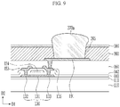
- FIGS. 5 , 6 , 7 , 8 , and 9 illustrate cross-sectional views of a display device manufactured by using a manufacturing method according to an exemplary embodiment.
- the transistor including the buffer layer 111, the semiconductor layer 130, the gate electrode 124, the source electrode 153, and the drain electrode 155, the first insulating film 141, the second insulating film 142, and the third insulating film 160 are formed on the substrate 110.
- the pixel electrode 191 connected to the drain electrode 155 is formed on the third insulating film 160.
- the third insulating film 160 and the partition wall 360 having the opening 365 in the pixel electrode 191 are formed.
- the opening 365 may expose a portion of the pixel electrode 191.
- the partition wall 360 may be formed by patterning a first material layer.
- the partition wall 360 including the opening 365 may be formed through a photolithography process.
- the first material layer may overlap a front surface of the substrate 110, and may include, for example, an organic material such as benzocyclobutene, a polyamide resin, a polyacrylic resin, a polyimide resin, and a phenol resin, or a siloxane-based inorganic material.
- an organic material such as benzocyclobutene, a polyamide resin, a polyacrylic resin, a polyimide resin, and a phenol resin, or a siloxane-based inorganic material.
- a residual film 361 is formed on the pixel electrode 191 by the first layer material forming the partition wall 360.
- a thickness of the residual film 361 e.g., a length from an upper surface of the residual film to a lower surface of the residual film in the second direction D2
- the residual film 361 is not removed, since the residual film 361 is disposed between the light emitting layer 370 and the pixel electrode 191, the light emitting efficiency and the light emitting lifetime of the light emitting device may be lowered.
- the residual film 361 described in FIG. 5 may be removed through a residual film removing process.
- a plasma process or a UVO 3 process may be used to remove the residual film 361.
- exemplary embodiments are not limited thereto and any method for removing the residual film may be performed.
- a second material layer 380a is applied so as to overlap the front surface of the substrate 110.
- the second material layer 380a may be disposed on upper surfaces and lateral edges of the partition wall 360 and the exposed surface of the pixel electrode 191.
- the second material layer 380a may include a compound and a resin that provide lyophobicity.
- the compound with lyophobicity may be in a form of a polymer or a monomer.
- the compound may include at least one of a fluorine-based compound and a siloxane-based compound.
- the fluorine-based compound may include, for example, a compound represented by Chemical Formula 1.
- the siloxane-based compound may include, for example, a compound represented by Chemical Formula 2.
- the resin may include, for example, a compound represented by Chemical Formula 3.
- a molecular weight of the monomer or polymer included in the second material layer 380a may be smaller than the molecular weight of the first material layer included in the partition wall 360.
- the compound having lyophobicity included in the second material layer 380a may be included in an amount of about 5 wt% or less with respect to a total content of the second material layer 380a.
- a mask (MASK) is disposed on the second material layer 380a, and a region not overlapping the mask (MASK) is cured. An uncured area may be subsequently removed by using a solvent.
- the same solvent as that included in the second material layer 380a may be used for removing the uncured second material layer.
- the solvent may include any solvent for removing the uncured second material layer 380a.
- the solvent may be an organic solvent.
- the solvent may be at least one of toluene, cyclopentanone, anisole, and propylene glycol methyl ether acetate (PGMEA).
- PMEA propylene glycol methyl ether acetate
- exemplary embodiments of the present inventive concepts are not limited thereto.
- the auxiliary layer 380 is then formed on the partition wall 360 and is not formed within the opening 365.
- the exemplary embodiment of FIG. 8 shows the auxiliary layer 380 as having an inclined lateral edge that is substantially aligned with the inclined lateral edge of the partition wall 360
- the auxiliary layer 380 may also be formed to have the shapes shown in the exemplary embodiments of FIG. 2 and FIG. 3 depending on the shape or alignment of the mask.
- a light emitting solution 370a for forming the light emitting layer on the opening 365 is subsequently provided.
- the light emitting solution 370a may be provided through a solution process, and for example, may be provided using inkjet printing.
- the lyophobic auxiliary layer 380 is formed at the upper end (e.g., in the second direction D2) of the partition wall 360, the light emitting solution 370a provided by the solution process may be stably positioned within the opening 365 of the partition wall 360 without overflowing the auxiliary layer 380.
- the solvent included in the light emitting solution 370a is removed through a drying process or the like and the light emitting layer 370 as shown in FIG. 1 may be formed. Thereafter, the common electrode 270 and the encapsulation layer 400 may be sequentially formed on the light emitting layer 370 to provide the display device as shown in FIG. 1 .
- the residual film removing process is performed after the auxiliary layer is formed, not only the residual film disposed on the pixel electrode but also the auxiliary layer disposed on the upper portion of the partition wall may be damaged. Therefore, the lyophobicity of the auxiliary layer may be lowered, and the light emitting solution provided for forming the light emitting layer may also overflow from the opening 365 to be positioned on the upper surface of the partition wall.
- the auxiliary layer having lyophobicity is formed after the residual film removing process is performed. Therefore, the auxiliary layer may stably provide lyophobicity to the upper surface of the partition wall to stably form the light emitting layer as well as to effectively remove the residual film that lowers the light emitting efficiency and the light emitting lifetime. Accordingly, it is possible to provide a display device having improved reliability.
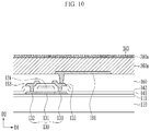
- FIGS. 10 , 11 , and 12 illustrate a cross-sectional view of a display device manufactured by using a manufacturing method according to exemplary embodiments.
- the transistor including the buffer layer 111, the semiconductor layer 130, the gate electrode 124, the source electrode 153, and the drain electrode 155, the first insulating film 141, the second insulating film 142, and the third insulating film 160, are formed on the substrate 110.
- the pixel electrode 191 connected to the drain electrode 155 is formed on the third insulating film 160.
- a first material layer 360a and the second material layer 380a overlapping the front surface of the substrate 110 are respectively formed on the third insulating film 160 and the pixel electrode 191.
- the first material layer 360a may include an organic material such as benzocyclobutene, a polyamide resin, a polyacrylic resin, a polyimide resin, a phenol resin, or a siloxane-based inorganic material.
- an organic material such as benzocyclobutene, a polyamide resin, a polyacrylic resin, a polyimide resin, a phenol resin, or a siloxane-based inorganic material.
- the second material layer 380a may include the plurality of nanoparticles 383.
- the second material layer 380a according to exemplary embodiments may not include a compound having lyophobicity, but is not limited thereto, and it may partially include a compound having lyophobicity.
- An upper surface of the second material layer 380a may be provided with protrusions and depressions.
- the protrusions and depressions may be formed by the plurality of nanoparticles 383.
- the partition wall 360 including the opening 365 and the auxiliary layer 380 are subsequently formed.
- the partition wall 360 and the auxiliary layer 380 may be manufactured through a photolithographic process.
- the residual film 361 generated while the first material layer is removed is formed on the exposed portion of the pixel electrode 191.
- the residual film 361 is a factor that degrades the light emitting efficiency and the light emitting lifetime of the light emitting element.
- the residual film 361 may be removed through a residual film removing process.
- the residual film removing process may be a plasma process or a UVO 3 process.
- exemplary embodiments of the present inventive concepts are not limited thereto.
- the auxiliary layer 380 since the auxiliary layer 380 has excellent resistance to a plasma or UVO 3 process by the plurality of nanoparticles 383, the auxiliary layer exhibits little surface damage from the residual film removing process.
- the upper portion of the partition wall 360 may maintain lyophobicity by the auxiliary layer 380, and only the unnecessary residual film 361 may be removed by the residual film removing process.
- the light emitting solution 370a for forming the light emitting layer may subsequently be injected onto the opening 365.
- the light emitting solution 370a may be provided through the solution process, and for example, may be provided through an inkjet process.
- the auxiliary layer 380 provided with the protrusions and depressions formed by the plurality of nanoparticles 383 is disposed at the upper surface of the partition wall 360. Since the protrusions and depressions of the auxiliary layer 380 provides lyophobicity, the light emitting solution 370a may be stably injected into the opening 365 without remaining at the upper end of the auxiliary layer 380. The light emitting solution 370a may be injected into the opening 365 without overflowing the upper portion of the partition wall 360.
- the light emitting layer 370 as shown in FIG 4 may be formed. Thereafter, the common electrode 270 and the encapsulation layer 400 may be sequentially formed on the light emitting layer 370 to provide the display device as shown in FIG. 4 .
- the auxiliary layer 380 including the plurality of nanoparticles 383 is formed before the residual film removing process
- embodiments of the present invention are not limited thereto, and the auxiliary layer 380 including the plurality of nanoparticles 383 may be formed subsequent to the residual film removing process as described for the exemplary embodiments of the manufacturing process of FIG. 5 to FIG. 9 .
- the auxiliary layer 380 including the plurality of nanoparticles 383 is resistant to damage caused by the residual film removing process. Therefore, the auxiliary layer 380 including the plurality of nanoparticles 383 may be formed before or after the residual film removing process.
- FIG. 13 illustrates a cross-sectional view of a display device according to an exemplary embodiment.
- the display device according to the exemplary embodiment of FIG. 13 includes the substrate 110, the buffer layer 111, the semiconductor layer 130, the first insulating film 141, the gate electrode 124, the second insulating film 142, the source electrode 153, the drain electrode 155, the third insulating film 160, the pixel electrode 191, the partition wall 360, the auxiliary layer 380, the light emitting layer 370, the common electrode 270, and the encapsulation layer 400, as previously described and a detailed description thereof will be omitted.
- the light emitting layer 370 may emit blue light.
- the color converting panel 20 includes a second substrate 210 overlapping (e.g., in the second direction D2) the first substrate 110.
- a red color filter 230R, a green color filter 230G, and a blue color filter 230B arranged in a first direction D1 may be disposed on the second substrate 210.
- the display device is provided with at least one light blocking member 220 surrounding the red color filter 230R, the green color filter 230G, and the blue color filter 230B.
- the red color filter 230R, green color filter 230G and the blue color filter 230B may be spaced apart in the first direction D1 and the light blocking member 220 may fill the spaces therebetween.
- the light blocking member 220 may prevent different light emitted from adjacent pixels from mixing with each other and may partition the area in which the red color filter 230R, the green color filter 230G, and the blue color filter 230B are disposed.
- a first flat film 240 is disposed between the light blocking members 220, the red color filter 230R, the green color filter 230G, and the blue color filter 230B, and the encapsulation layer 400.
- the first flat film 240 may be disposed directly below a lower surface (e.g., in the second direction D2) of the light blocking members 220, the red color filter 230R, the green color filter 230G, and the blue color filter 230B.
- the first flat film 240 may be a film for flattening (e.g., planarizing) a surface of the light blocking member 220, the red color filter 230R, the green color filter 230G, and the blue color filter 230B.
- the first flat film 240 may flatten the lower surface (e.g., in the second direction D2) of the light blocking member 220, the red color filter 230R, the green color filter 230G, and the blue color filter 230B.
- the first flat film 240 may include at least one of an organic insulating material and an inorganic insulating material.
- the red color converting layer 250R, the green color converting layer 250G, and the transmissive layer 250B may be disposed between the first flat film 240 and the encapsulation layer 400.
- the red color converting layer 250R, the green color converting layer 250G, and the transmissive layer 250B may be disposed directly below a lower surface (e.g., in the second direction D2) of the first flat film 240.
- the red color conversion layer 250R, the green color conversion layer 250G, and the transmissive layer 250B may be repeatedly arranged along the first direction D1 and may be spaced apart from each other. For example, as shown in FIG. 13 , spaces between the color conversion layers may overlap (e.g., in the second direction D2) with the light blocking members 220.
- the red color conversion layer 250R and the green color conversion layer 250G convert light emitted from the light emitting layer 370 and emit the light.
- the red color conversion layer 250R may convert blue light emitted from the light emitting layer 370 into red light.
- the red color conversion layer 250R may include a first semiconductor nanocrystal 251R that converts blue light incident from the light emitting layer 370 into red light.
- the first semiconductor nanocrystal 251R may include at least one of a phosphor and a quantum dot.
- the green color conversion layer 250G may convert blue light emitted from the light emitting layer 370 into green light.
- the green color conversion layer 250G may include a second semiconductor nanocrystal 251G that converts blue light incident from the light emitting layer 370 into green light.
- the second semiconductor nanocrystal 251G may include at least one of a phosphor and a quantum dot.
- the transmissive layer 250B emits incident light from the light emitting layer 370 without conversion of the incident light. For example, blue light may be incident on the transmissive layer 250B and may be emitted as it is without conversion by the transmissive layer.
- the quantum dot included in the first semiconductor nanocrystal 251R and the second semiconductor nanocrystal 251G may be independently selected from a Group II-VI compound, a Group III-V compound, a Group IV-VI compound, a Group IV element, a Group IV compound, and a combination thereof.
- the specific compounds are the same as those described above with respect to the quantum dot of the light emitting layer 370.
- the transmissive layer 250B may transmit incident light as it is.
- the transmissive layer 250B may include a resin that transmits blue light.
- the transmissive layer 250B disposed in a region that emits blue light does not include any separate semiconductor nanocrystal.
- the transmissive layer 250B may further include at least one of a dye and a pigment.
- the transmissive layer 250B including the dye or pigment may reduce the external light reflection, and may provide the blue light with improved color purity.
- At least one of the red color conversion layer 250R, the green color conversion layer 250G, and the transmissive layer 250B may further include scatterers 252.
- the contents of the respective scatterers 252 included in the red color conversion layer 250R, the green color conversion layer 250G and the transmissive layer 250B may be different.
- the scatterers 252 may increase an amount of light that is converted in or passes through the color conversion layers 250R and 250G and the transmissive layer 250B and then is emitted through the color conversion layers and the transmissive layer.
- the scatterers 252 may uniformly provide front luminance and lateral luminance for the light emitted from the light emitting layer 370.
- the scatterers 252 may include any material capable of evenly scattering incident light.
- the scatterers 332 may include at least one among TiO2, ZrO2, Al2O3, In2O3, ZnO, SnO2, Sb2O3, and ITO.
- the red color conversion layer 250R, the green color conversion layer 250G, and the transmissive layer 250B may include a photosensitive resin, and may be formed through a photolithography process.
- exemplary embodiments of the present inventive concepts are not limited thereto.
- the red color conversion layer 250R, the green color conversion layer 250G, and the transmissive layer 250B may be formed through a printing process or an inkjet process, and the red color conversion layer, the green color conversion layer and the transmissive layer may include a material that is not the photosensitive resin.
- the color conversion layer and the transmissive layer are formed through the photolithography process, the printing process, or the inkjet process, exemplary embodiments of the present inventive concepts are not limited thereto.
- the red color conversion layer 250R may overlap the red color filter 230R in the second direction D2
- the green color conversion layer 250G may overlap the green color filter 230G in the second direction D2
- the transmissive layer 250B may overlap the blue color filter 230B in the second direction D2.
- a second flat film 260 is disposed in lateral spaces between the red color conversion layer 250R, the green color conversion layer 250G and the transmissive layer 250B and between lower surfaces of the color conversion layers and an upper surface of the encapsulation layer 400.
- the second flat film 260 may overlap a front surface of the second substrate 210.
- the second flat film 260 may flatten (e.g., planarize) one surface of the red color conversion layer 250R, the green color conversion layer 250G, and the transmissive layer 250B.
- the second flat film 260 may include an organic insulating material or an inorganic insulating material.
- exemplary embodiments of the present inventive concepts are not limited thereto and the second flat film 260 may include any material capable of performing a flattening function.
- the encapsulation layer 400 and the color converting panel 20 are in direct contact with each other.
- exemplary embodiments of the present inventive concepts are not limited thereto.
- a separate filling layer may be disposed between the encapsulation layer 400 and the color converting panel 20.
- the encapsulation layer 400 and the color converting panel 20 may be combined through various known methods and structures, such as by a separate adhesive layer or by a sealant along an edge of the display device.
- the present specification may include a filter layer positioned between the color conversion layers 250R and 250G and the encapsulation layer 400 to emit light of a specific wavelength, or may include a second substrate 210 and the color conversion layers 250R and 250G, and a blue light blocking filter positioned between the second substrate and the transmissive layer 250B.
- embodiments can provide a display device comprising a partition wall disposed on a substrate between a first electrode and a second electrode, the partition wall having an opening; a light emitting layer disposed in the opening; and an auxiliary layer having lyophobicity disposed between the partition wall and the second electrode.
- the auxiliary layer may have lyophobicity with respect to a solvent used to form the light emitting layer in a solution process during manufacture.
- the solvent in the solution process may be an organic solvent.
- the solvent may be at least one of toluene, cyclopentanone, anisole, and propylene glycol methyl ether acetate (PGMEA).
- the auxiliary layer may have a higher degree of lyophobicity than the material of the partition wall (which may, for example, be lyophilic), for example with respect to an organic solvent used in forming the light emitting layer in a solution process. Hence, the auxiliary layer may repel the organic solvent more than the partition wall.
- the partition wall may be a pixel defining layer.
- the auxiliary layer may be formed over a portion of an upper surface of the partition wall.
- the auxiliary layer may be spaced apart from the opening. In some embodiments, the auxiliary layer is not formed in the region of the opening (e.g. on side surfaces of opening or over the first electrode in the region of the opening).
- the opening of the partition wall may correspond to the first electrode, which may be a pixel electrode for a pixel.
- the second electrode may correspond to a common electrode for a plurality of pixels.
- the first electrode, the light emitting layer, and the second electrode may form a light emitting diode, and the opening may at least partially overlap the first electrode.
- a portion of the partition wall may overlap the first electrode.
- the display device may comprise a plurality of pixels, each corresponding to respective openings in the partition wall, and each pixel having a first electrode (e.g. a pixel electrode), a second electrode (e.g. a common electrode) and a light emitting layer therebetween.
- a first electrode e.g. a pixel electrode
- a second electrode e.g. a common electrode
- the partition wall may include an organic material (e.g. one that is lyophilic).
- a light emitting solution for forming the light emitting layer may contact the auxiliary layer.
- the auxiliary layer has lyophobicity, the light emitting solution may be forced away from the auxiliary layer and may be stably positioned in the opening of the (e.g. lyophilic) partition wall rather than being positioned on the auxiliary layer.
- the light emitting solution may be positioned in the opening without contacting the auxiliary layer, and particularly, it may form a stable light emitting layer that does not flow over from the opening.
- the auxiliary layer may include at least one of a fluorine-based compound and a siloxane-based compound.
- the auxiliary layer may include a plurality of nanoparticles, and a surface of the auxiliary layer facing the second electrode may be provided with protrusions and depressions.
- Embodiments can provide a method of manufacturing a display device comprising forming a first electrode over a substrate, forming partition wall having an opening over the first electrode, forming an auxiliary layer having lyophobicity over the partition wall (either before or after forming the opening), forming a light emitting layer using a solution process, and forming a second electrode over the partition wall.
Landscapes
- Engineering & Computer Science (AREA)
- Microelectronics & Electronic Packaging (AREA)
- Manufacturing & Machinery (AREA)
- Electroluminescent Light Sources (AREA)
Abstract
Description
- The present disclosure relates to a display device and a manufacturing method thereof.
- A light emitting display device includes two electrodes and a light emitting layer disposed therebetween. An electron injected from one electrode that serves as a cathode, and a hole injected from the other electrode which serves as an anode are coupled with each other in the light emitting layer to generate an exciton. The exciton emits energy to emit light.
- The light emitting display device includes a plurality of pixels having a light emitting diode including a cathode, an anode, and a light emitting layer, and each pixel includes a plurality of transistors and capacitors for driving the light emitting diode.
- The above information is only for enhancement of understanding of the present inventive concepts, and therefore may contain information that does not form the prior art and which is already known in the relevant art.
- Exemplary embodiments provide a display device and a manufacturing method thereof that may stably include a light emitting layer formed by a solution process by providing an auxiliary layer that is effectively formed while providing lyophobicity on a partition wall.
- An exemplary embodiment provides a display device including a partition wall disposed on a substrate between a first electrode and a second electrode. The partition wall has an opening. A light emitting layer is disposed in the opening. An auxiliary layer having lyophobicity is disposed between the partition wall and the second electrode.
- A maximum thickness of the auxiliary layer may be about 100 nm or more and about 200 nm or less.
- A maximum thickness of the partition wall may be about 1 µm or more and about 1.5 µm or less.
- The auxiliary layer may not overlap the opening.
- The auxiliary layer may include at least one of a fluorine-based compound and a siloxane-based compound.
- The fluorine-based compound may be represented by Chemical Formula 1, and the siloxane-based compound may be represented by Chemical Formula 2.


- A lateral edge of the auxiliary layer is inclined and is aligned with an inclined lateral edge of the partition wall.
- The auxiliary layer may expose a portion of an upper surface of the partition wall.
- The auxiliary layer may overlap a lateral surface of the partition wall.
- The light emitting layer may include a quantum dot.
- The display device may further include a red color converting layer, a green color converting layer, and a transmissive layer that overlaps the light emission layer.
- Each of the red color converting layer and the green color converting layer may include a quantum dot.
- Another exemplary embodiment provides a display device including a partition wall disposed on a substrate between a first electrode and a second electrode. The partition wall has an opening. A light emitting layer is disposed in the opening. An auxiliary layer is disposed between the partition wall and the second electrode. The auxiliary layer includes a plurality of nanoparticles, and a surface of the auxiliary layer facing the second electrode is provided with protrusions and depressions.
- A thickness of the auxiliary layer may be about 30 nm to about 200 nm.
- The plurality of nanoparticles may include silica nanoparticles.
- Another exemplary embodiment provides a manufacturing method of a display device, including forming a thin film transistor and a pixel electrode connected to the thin film transistor on a substrate. A first material layer is formed overlapping the pixel electrode on the substrate. The first material layer is etched to form a partition wall including an opening. A residual film that is formed on the pixel electrode is removed. An auxiliary layer is formed having lyophobicity on the partition wall.
- The removing of the residual film may use at least one of a plasma process and a UVO3 process.
- The forming of the auxiliary layer may include forming a second material layer on the partition wall, and removing an uncured area in the second material layer, and the removing of the uncured area may use an organic solvent.
- The organic solvent may include at least one of toluene, cyclopentanone, anisole, and propylene glycol methyl ether acetate (PGMEA).
- The second material layer may include the same solvent as the organic solvent.
- The manufacturing method of the display device may further include providing a light emitting solution on the opening, and drying the light emitting solution to form a light emitting layer.
- Another exemplary embodiment provides a manufacturing method of a display device, including forming a thin film transistor and a pixel electrode connected to the thin film transistor on a substrate. A first material layer and a second material layer are sequentially formed overlapping the substrate on the pixel electrode. The first material layer and the second material layer are etched to form a partition wall having an opening and an auxiliary layer. A residual film formed on the pixel electrode is removed. The second material layer may include a plurality of nanoparticles.
- According to an aspect, there is provided a display device as set out in claim 1. Additional features of this aspect are set out in claims 2 to 15.
- According to exemplary embodiments of the present inventive concepts, it is possible to stably form a light emitting layer through a solution process by including an auxiliary layer that is stably formed on an upper surface of a partition wall and has lyophobicity. Reliability of a light emitting diode and a display device including such a light emitting layer may be improved.
-
-
FIG. 1 illustrates a cross-sectional view of a display device according to an exemplary embodiment of the present inventive concepts. -
FIG. 2 illustrates a cross-sectional view of a display device according to an exemplary embodiment of the present inventive concepts. -
FIG. 3 illustrates a cross-sectional view of a display device according to an exemplary embodiment of the present inventive concepts. -
FIG. 4 illustrates a cross-sectional view of a display device according to an exemplary embodiment of the present inventive concepts. -
FIGS. 5 ,6 ,7 ,8 , and9 illustrate cross-sectional views of a display device manufactured by using a manufacturing method according to exemplary embodiments of the present inventive concepts. -
FIGS. 10 ,11 , and12 illustrate a schematic cross-sectional view of a display device manufactured by using a manufacturing method according to exemplary embodiments of the present inventive concepts. -
FIG. 13 illustrates a schematic cross-sectional view of a display device according to an exemplary embodiment of the present inventive concepts. - The present invention will be described more fully hereinafter with reference to the accompanying drawings, in which exemplary embodiments of the invention are shown. As those skilled in the art would realize, the described embodiments may be modified in various different ways, all without departing from the spirit or scope of the present disclosure.
- Parts that are irrelevant to the description will be omitted to clearly describe the present disclosure, and like reference numerals designate like elements throughout the specification.
- Further, in the drawings, the size and thickness of each element are arbitrarily illustrated for ease of description, and the present disclosure is not necessarily limited to those illustrated in the drawings. In the drawings, the thicknesses of layers, films, panels, regions, etc., may be exaggerated for clarity. In the drawings, for ease of description, the thicknesses of some layers and areas are exaggerated.
- It will be understood that when an element such as a layer, film, region, or substrate is referred to as being "on" another element, it can be directly on the other element or intervening elements may also be present. In contrast, when an element is referred to as being "directly on" another element, there are no intervening elements present. Further, in the specification, the word "on" or "above" means disposed on or below the object portion, and does not necessarily mean disposed on the upper side of the object portion based on a gravitational direction.
- In addition, unless explicitly described to the contrary, the word "comprise" and variations such as "comprises" or "comprising" will be understood to imply the inclusion of stated elements but not the exclusion of any other elements.
- Further, throughout the specification, the phrase "on a plane" means viewing a target portion from the top, and the phrase "on a cross-section" means viewing a cross-section formed by vertically cutting a target portion from the side.
- Hereinafter, a display device according to an exemplary embodiment of the present invention will be described.
FIG. 1 illustrates a cross-sectional view of a display device according to an exemplary embodiment of the present inventive concepts. - Referring to
FIG. 1 , asubstrate 110 may include a transparent glass substrate. However, in another exemplary embodiment, thesubstrate 110 may include a plastic layer and a barrier layer that are alternately stacked. Thesubstrate 110 according to an exemplary embodiment may be a flexible substrate which may be bent, folded, rolled, etc. - A
buffer layer 111 is disposed on thesubstrate 110. Thebuffer layer 111 may prevent impurities or the like from diffusing from thesubstrate 110 toward the inside of the display device. In addition, thebuffer layer 111 may improve a flatness of a surface of the substrate 110 (e.g., planarize the surface of the substrate) in embodiments in which the surface of thesubstrate 110 is not uniform. - The
buffer layer 111 may include an inorganic insulating material such as a silicon oxide, a silicon nitride, or the like. However, in some exemplary embodiments, thebuffer layer 111 may include an organic insulating material. Thebuffer layer 111 may be a single layer or have a multilayer structure. For example, in an exemplary embodiment in which thebuffer layer 111 is a dual layer, a lower layer thereof may include a silicon nitride and an upper layer thereof may include a silicon oxide. However, exemplary embodiments of the present inventive concepts are not limited thereto. - A
semiconductor layer 130 is disposed on thebuffer layer 111. In an exemplary embodiment, thesemiconductor layer 130 may include amorphous silicon, polycrystalline silicon, an oxide semiconductor, and the like. However, exemplary embodiments of the present inventive concepts are not limited thereto. - The
semiconductor layer 130 may include asource region 132 connected to asource electrode 153, adrain region 133 connected to adrain electrode 155, and achannel region 131 disposed between thesource region 132 and thedrain region 133, which will be described later. Thesource region 132 and thedrain region 133 may be doped with an impurity. - A first insulating
film 141 is disposed on thesemiconductor layer 130 and thebuffer layer 111. For example, as shown inFIG. 1 , the first insulatingfilm 141 may be disposed directly on upper surfaces (e.g., in the second direction D2) of thesemiconductor layer 130 andbuffer layer 111. The firstinsulating film 141 may include an inorganic insulating material such as a silicon nitride, a silicon oxide, a metal oxide, or the like. However, in some exemplary embodiments, the first insulatingfilm 141 may include an organic insulating material. - A
gate electrode 124 is disposed on the first insulatingfilm 141. For example, as shown inFIG. 1 , thegate electrode 124 may be disposed directly on an upper surface (e.g., in the second direction D2) of the first insulatingfilm 141. Thegate electrode 124 overlaps (e.g., in the second direction D2) thechannel region 131 of thesemiconductor layer 130. - The
gate electrode 124 may include at least one material selected from aluminum (Al), platinum (Pt), palladium (Pd), silver (Ag), magnesium (Mg), gold (Au), nickel (Ni), neodymium (Nd), iridium (Ir), chromium (Cr), lithium (Li), calcium (Ca), molybdenum (Mo), titanium (Ti), tungsten (W), and copper (Cu). Thegate electrode 124 may include a single layer or a multilayer structure. - A second
insulating film 142 may be disposed on thegate electrode 124 and the first insulatingfilm 141. For example, the secondinsulating film 142 may be disposed directly on an upper surface (e.g., in the second direction D2) of the first insulatingfilm 141. The secondinsulating film 142 may include an inorganic insulating material such as a silicon nitride, a silicon oxide or the like. However, in some exemplary embodiments, the secondinsulating film 142 may include an organic insulating material. - The
source electrode 153 and thedrain electrode 155 may be disposed on the secondinsulating film 142. For example, as shown inFIG. 1 , thesource electrode 153 and thedrain electrode 155 may be disposed directly on an upper surface (e.g., in the second direction D2) of the secondinsulating film 142. - The
source electrode 153 and thegate electrode 155 may include at least one material selected from aluminum (Al), platinum (Pt), palladium (Pd), silver (Ag), magnesium (Mg), gold (Au), nickel (Ni), neodymium (Nd), iridium (Ir), chromium (Cr), lithium (Li), calcium (Ca), molybdenum (Mo), titanium (Ti), tungsten (W), and copper (Cu). Thesource electrode 153 and thedrain electrode 155 may include a single layer or a multilayer structure. - The
source electrode 153 and thedrain electrode 155 may be connected to thesource region 132 and thedrain region 133 of thesemiconductor layer 130, respectively, through contact holes formed in the first insulatingfilm 141 and the secondinsulating film 142. - A third
insulating film 160 is disposed on thesource electrode 153 and thedrain electrode 155. The thirdinsulating film 160 may cover thesource electrode 153 and thedrain electrode 155 for planarization thereof. The thirdinsulating film 160 may include an organic insulating material or an inorganic insulating material. - The first electrode, which is a
pixel electrode 191, is disposed on the thirdinsulating film 160. For example, as shown inFIG. 1 , thepixel electrode 191 may be disposed directly on an upper surface (e.g., in the second direction D2) of the thirdinsulating film 160. Thepixel electrode 191 may be connected to thedrain electrode 155 through a contact hole formed in the thirdinsulating film 160. - The
pixel electrode 191 may be a transparent electrode, a transflective electrode, or a reflective electrode. In embodiments in which thepixel electrode 191 is a transparent electrode or a transflective electrode, thepixel electrode 191 may be formed of ITO, IZO, ZnO, In2O3, IGO, or AZO. In embodiments in which thepixel electrode 191 is a reflective electrode, thepixel electrode 191 may include a reflective film including Ag, Mg, Al, Pt, Pd, Au, Ni, Nd, Ir, Cr, and a compound thereof, and a layer including ITO, IZO, ZnO, In2O3, IGO, or AZO. However, exemplary embodiments of thepixel electrode 191 are not limited thereto, and thepixel electrode 191 may include various materials, and may have variously modified structures such as a single layer structure or a multi-layer structure. - A
partition wall 360 is disposed on thepixel electrode 191 and the thirdinsulating film 160. For example, as shown inFIG. 1 , thepartition wall 360 may be disposed directly on an upper surface (e.g., in the second direction D2) and lateral edge surfaces of thepixel electrode 191 and an upper surface of the thirdinsulating film 160. Thepartition wall 360 includes anopening 365 that exposes a portion of thepixel electrode 191. Alight emitting layer 370 may be disposed in theopening 365. For example, as shown inFIG. 1 , thelight emitting layer 370 may be disposed directly on the portion of thepixel electrode 191 exposed by theopening 365. An exposed region of thepixel electrode 191 having the light emitting layer thereon may be a light emitting region and a region in which thepartition wall 360 covers the pixel electrode may be a non-light emitting region. Hence, thepartition wall 360 may be a pixel defining layer. - In an exemplary embodiment, the
partition wall 360 may be lyophilic. In a process in which a light emitting solution is provided in theopening 365, the light emitting solution may be stably injected into the opening, adjacent to thelyophilic partition wall 360. Thelyophilic partition wall 360 may help stably position the light emitting solution within theopening 365. - The
partition wall 360 may include an organic material. For example, in an exemplary embodiment, the organic material may be benzocyclobutene, a polyamide resin, a polyacrylic resin, a polyimide resin, a phenol resin, or a siloxane-based inorganic material. However, exemplary embodiments of the present inventive concepts are not limited thereto. Thepartition wall 360 may additionally include at least one of an initiator, a crosslinking agent, a photoactive agent, and a surfactant. Thepartition wall 360 may include a photoactive agent when it includes a positive photoresist, and thepartition wall 360 may include an initiator when it includes a negative photoresist. - A maximum thickness t1 of the partition wall 360 (e.g., the length from a top surface of the partition wall to a bottom surface of the partition wall in the second direction D2) may be about 1 µm to about 1.5 µm. Lateral edges of the
partition wall 360 forming the opening may have a tapered shape toward thesubstrate 110. For example, theopening 365 may expose lateral edges of thepartition wall 360 which are spaced farther apart as the distance from the substrate increases. The thickness t1 of thepartition wall 360 in the flat region which does not include the inclined lateral edges of the partition wall may be about 1 µm to about 1.5 µm. In embodiments in which the thickness of thepartition wall 360 is less than about 1 µm, a distinction between a light emitting region in which the light emitting layer is disposed and a non-light emitting region in which a light emitting layer is not disposed is not clear and a resolution of the display device may be lowered. In embodiments in which the thickness of thepartition wall 360 is greater than about 1.5 µm, it is difficult for other components that are stacked on thepartition 360 to have a uniform profile in a continuous shape. - The
light emitting layer 370 is disposed on thepixel electrode 191 exposed by theopening 365 as described above. Acommon electrode 270 is disposed on thelight emitting layer 370 and thepartition wall 360. For example, as shown inFIG. 1 , thecommon electrode 270 may be disposed directly on an upper surface (e.g., in the second direction D2) of thelight emitting layer 370 and thepartition wall 360. - The
pixel electrode 191, thelight emitting layer 370, and thecommon electrode 270 may form a light emitting diode. Thecommon electrode 270 may be a transparent electrode, a transflective electrode, or a reflective electrode. - When the
common electrode 270 is a transparent electrode or a transflective electrode, thecommon electrode 270 may include a layer including a metal having a small work function, such as Li, Ca, LiF/Ca, LiF/Al, Al, Ag, Mg, and a compound thereof, and a transparent layer such as ITO, IZO, ZnO, or In2O3, or a transflective conductive layer. When thecommon electrode 270 is a reflective electrode, it may include, for example, a layer including Li, Ca, LiF/Ca, LiF/Al, Al, Ag, Mg, and a compound thereof. However, the materials and the stacked structure of thecommon electrode 270 are not limited thereto, and exemplary embodiments of the present inventive concepts may have various modifications and arrangements. - The
pixel electrode 191 is an anode that is a hole injection electrode, and thecommon electrode 270 is a cathode that is an electron injection electrode. However, exemplary embodiments of the present inventive concepts are not limited thereto. For example, in other exemplary embodiments, thepixel electrode 191 may be a cathode and thecommon electrode 270 may be an anode according to a driving method of the display device. Holes and electrons are injected into thelight emitting layer 370 from thepixel electrode 191 and thecommon electrode 270, respectively, and exitons generated by coupling the injected holes and electrons fall from an excited state to a ground state to emit light. - In an exemplary embodiment, the
light emitting layer 370 may include a low molecular organic material or a polymer organic material such as poly(3,4-ethylenedioxythiophene) (PEDOT). Thelight emitting layer 370 may include a multilayer structure that includes a light emitting layer and at least one of a hole injecting layer, a hole transporting layer, an electron transporting layer, and an electron injecting layer. In embodiments in which all of these layers are included, the hole injecting layer is disposed on thepixel electrode 191, which is an anode, and the hole transporting layer, the light emitting layer, the electron transporting layer, and an electron injecting layer may be sequentially stacked thereon. - The
light emitting layer 370 according to the exemplary embodiment may include a quantum dot. The quantum dot may emit red light, green light, or blue light. In an exemplary embodiment, a core of the quantum dot may be selected from Group II-VI compounds, Group III-V compounds, Group IV-VI compounds, Group IV elements, Group IV compounds, and combinations thereof. - The Group II-VI compound may be selected from: a two-element compound selected from CdSe, CdTe, ZnS, ZnSe, ZnTe, ZnO, HgS, HgSe, HgTe, MgSe, MgS, and a mixture thereof; a three-element compound selected from CdSeS, CdSeTe, CdSTe, ZnSeS, ZnSeTe, ZnSTe, HgSeS, HgSeTe, HgSTe, CdZnS, CdZnSe, CdZnTe, CdHgS, CdHgSe, CdHgTe, HgZnS, HgZnSe, HgZnTe, MgZnSe, MgZnS, and a mixture thereof; and a four-element compound selected from HgZnTeS, CdZnSeS, CdZnSeTe, CdZnSTe, CdHgSeS, CdHgSeTe, CdHgSTe, HgZnSeS, HgZnSeTe, HgZnSTe, and a mixture thereof.
- The Group III-V compound may be selected from: a two-element compound selected from GaN, GaP, GaAs, GaSb, AlN, AlP, AlAs, AlSb, InN, InP, InAs, InSb, and a mixture thereof; a three-element compound selected from GaNP, GaNAs, GaNSb, GaPAs, GaPSb, AlNP, AlNAs, AlNSb, AlPAs, AlPSb, InGaP, InNP, InNAs, InNSb, InPAs, InPSb, GaAlNP, and a mixture thereof; and a four-element compound selected from GaAlNAs, GaAlNSb, GaAlPAs, GaAlPSb, GaInNP, GaInNAs, GaInNSb, GaInPAs, GaInPSb, InAlNP, InAlNAs, InAlNSb, InAlPAs, InAlPSb, and a mixture thereof.
- The Group IV-VI compound may be selected from: a two-element compound selected from SnS, SnSe, SnTe, PbS, PbSe, PbTe, and a mixture thereof; a three-element compound selected from SnSeS, SnSeTe, SnSTe, PbSeS, PbSeTe, PbSTe, SnPbS, SnPbSe, SnPbTe, and a mixture thereof; and a four-element compound selected from SnPbSSe, SnPbSeTe, SnPbSTe, and a mixture thereof. The Group IV element may be selected from Si, Ge, and a mixture thereof. For example, the Group IV compound may be a two-element compound selected from SiC, SiGe, and a mixture thereof.
- The two-element compound, the three-element compound, or the four-element compound may be present in particles of the quantum dots at uniform concentrations, or they may be divided into states having partially different concentrations to be present in the same particle, respectively. In addition, a core/shell structure in which some quantum dots enclose some other quantum dots may be possible. In an exemplary embodiment, an interface between the core and the shell may have a concentration gradient in which a concentration of elements of the shell decreases as the distance to the shell center decreases.
- In some exemplary embodiments, the quantum dot may have a core-shell structure that includes a core including the nanocrystal described above and a shell surrounding the core. The shell of the quantum dot may serve as a passivation layer for maintaining a semiconductor characteristic and/or as a charging layer for applying an electrophoretic characteristic to the quantum dot by preventing chemical denaturation of the core. The shell may be a single layer or have a multilayer structure. An example of the shell of the quantum dot includes a metal or nonmetal oxide, a semiconductor compound, or a combination thereof.
- For example, the metal or nonmetal oxide may be a two-element compound such as SiO2, Al2O3, TiO2, ZnO, MnO, Mn2O3, Mn3O4, CuO, FeO, Fe2O3, Fe3O4, CoO, Co3O4, NiO, and the like, or a three-element compound such as MgAl2O4, CoFe2O4, NiFe2O4, CoMn2O4, and the like. However, exemplary embodiments of the present inventive concepts are not limited thereto.
- In addition, the semiconductor compound may be CdS, CdSe, CdTe, ZnS, ZnSe, ZnTe, ZnSeS, ZnTeS, GaAs, GaP, GaSb, HgS, HgSe, HgTe, InAs, InP, InGaP, InSb, AlAs, AlP, AlSb, or the like. However, exemplary embodiments of the present inventive concepts are not limited thereto.
- The quantum dot may have a full width at half maximum (FWHM) of the light-emitting wavelength spectrum that is equal to or less than about 45 nm. For example the quantum dot may have a FWHM equal to or less than about 40 nm. In another exemplary embodiment, the quantum dot may have a FWHM equal to or less than about 30 nm. In this range, color purity or color reproducibility of the display device may be improved. In addition, since light emitted through the quantum dot is emitted in all directions, a viewing angle of the transmitted light may be improved.
- Further, a shape of the quantum dot is not particularly limited in embodiments and may include a spherical, pyramidal, multi-arm, or cubic nanoparticle, nanotube, nano-wire, nano-fiber, nano-plate particle shape, and the like.
- The quantum dot may control a color of emitted light according to a particle size thereof. Therefore, the quantum dot may have various light emitting colors such as blue, red, and green colors.
- The
light emitting layer 370 may be formed by a solution process. For example, thelight emitting layer 370 may be formed by using any one of the following processes: spin coating, inkjet printing, gravure printing, roll-to-roll printing, syringe injection, dip coating, spray coating, relief printing, and screen printing. - In an exemplary embodiment, an
auxiliary layer 380 is disposed between thecommon electrode 270 and thepartition wall 360. Theauxiliary layer 380 may be disposed on an upper surface of thepartition wall 360. For example, as shown inFIG. 1 , a lower surface (e.g., in the second direction D2) of theauxiliary layer 380 may be disposed directly on an upper surface of thepartition wall 360 and an upper surface of theauxiliary layer 380 may contact a lower surface of thecommon electrode 270. Theauxiliary layer 380 may not overlap theopening 365 of thepartition wall 360 in the second direction D2. Theauxiliary layer 380 may not overlap lateral edge surfaces of thepartition wall 360 in the second direction D2. Theauxiliary layer 380 may be generally spaced apart in the first direction D1 from theopening 365 of the partition wall. However, as described in more detail later, in an exemplary embodiment, the lower surface of the lateral edge of the auxiliary layer may substantially overlap (e.g., in the second direction D2) the upper surface of the lateral edge of the partition wall. - The
auxiliary layer 380 according to an exemplary embodiment may have lyophobicity. For example, theauxiliary layer 380 may include a composition having lyophobicity. During a manufacturing process of the display device in which the light emitting layer is formed through a solution process, a light emitting solution for forming thelight emitting layer 370 may contact theauxiliary layer 380. However, since theauxiliary layer 380 has lyophobicity, the light emitting solution (e.g. solvent for the light emitting layer) may be forced away from theauxiliary layer 380 and may be stably positioned in theopening 365 of thelyophilic partition wall 360 rather than being positioned on the auxiliary layer. In other words, theauxiliary layer 380 may repel the light emitting solution. The light emitting solution may be positioned in theopening 365 without contacting theauxiliary layer 380, and particularly, it may form a stablelight emitting layer 370 that does not flow over from theopening 365. Therefore, the reliability of the light emitting diode including thelight emitting layer 370 and the display device may thereby be improved. - In the present specification, the lyophobicity means a property of pushing out a solution and not allowing the solution to penetrate well (i.e. "solvent rejecting"), and the word "lyophilic" means a property of having an affinity for a solution (i.e. "solvent preferring"). For example, a solution may have a low surface bonding force with one surface having a lyophobic property and may have an excellent surface bonding force with another surface being lyophilic. Therefore, according to exemplary embodiments of the present inventive concepts, the surface bonding force between the light emitting solution and the
auxiliary layer 380 may be weaker than the surface bonding force between the light emitting solution and thepartition wall 360. A contact angle of the light emitting solution with respect to theauxiliary layer 380 may be, for example, about 40 degrees or more. - The
auxiliary layer 380 may include a material that is lyophobic to the light emitting solution. In an exemplary embodiment, theauxiliary layer 380 may include a monomer or polymer. For example, theauxiliary layer 380 may include a fluorine-based compound or a siloxane-based compound. However, in other embodiments, theauxiliary layer 380 may include any compound having lyophobicity. The fluorine-based compound may be represented by Chemical Formula 1, and the siloxane-based compound may be represented by Chemical Formula 2. However, exemplary embodiments of the present inventive concepts are not limited thereto.

- A maximum thickness t2 of the
auxiliary layer 380 may be about 100 nm to about 200 nm or less. For example, the maximum thickness t2 of theauxiliary layer 380 may be between about 120 nm to about 180 nm or less. Considering that the maximum thickness t1 of thepartition wall 360 is about 1 µm to about 1.5 µm, theauxiliary layer 380 is considerably thinner than the partition wall. Theauxiliary layer 380 may be formed to be a thin layer for providing lyophobicity to the upper surface of thepartition wall 360. - In embodiments in which the thickness of the
auxiliary layer 380 is less than 100 nm, it may be difficult to substantially form a layer that has lyophobicity. In addition, the thickness of theauxiliary layer 380 may not exceed 200 nm so that theauxiliary layer 380 is sufficiently lyophobic and the light emitting solution forming thelight emitting layer 370 is stably positioned on theopening 365. In embodiments in which the thickness of theauxiliary layer 380 exceeds 200 nm, the light emitting solution injected into theopening 365 may be excessively swollen, and the light emitting solution may flow into an adjacent opening for mixture with the contents therein and may not be stably positioned in the opening. - In addition, the
auxiliary layer 380 may have surface energy of about 15 dyne/cm or less, the light emitting solution for forming thelight emitting layer 370 may have surface energy of about 17 to 35 dyne/cm, and thepixel electrode 191 may have surface energy of about 40 dyne/cm. Thepartition wall 360 may have surface energy of about 30 dyne/cm to about 43 dyne/cm. The surface energy of thepartition wall 360 may be greater than the surface energies of thelight emitting layer 370 and theauxiliary layer 380, and may be smaller than the surface energy of thepixel electrode 191. - The
auxiliary layer 380 is disposed on thepartition wall 360, and may form a separate layer from thepartition wall 360. Since theauxiliary layer 380 is formed through a separate manufacturing process from that of thepartition wall 360, an interface may be formed between thepartition wall 360 and theauxiliary layer 380. - In addition, the
lateral edge 381 of theauxiliary layer 380 may inclined so that is substantially aligned with the inclined lateral edge of thepartition wall 360. The lower surface of thelateral edge 381 of theauxiliary layer 380 and the upper surface of the lateral edge of thepartition wall 360 may substantially overlap (e.g., in the second direction D2). In an exemplary embodiment, theauxiliary layer 380 may be manufactured by using a same mask as a mask used for forming thepartition wall 360 in a manufacturing process. - In embodiments in which the light emitting solution is provided on the
substrate 110 by a solution process, such as an inkjet process, the light emitting solution is not positioned on an upper surface of the lyophobicauxiliary layer 380 and may be stably provided in theopening 365 included in thepartition wall 360. The lyophobicauxiliary layer 380 prevents the light emitting solution from overflowing thepartition wall 360. Therefore, thelight emitting layer 370 may have improved reliability, and a light emitting diode and a display device with improved reliability may be provided. - An
encapsulation layer 400 for protecting the light emitting diode may be disposed on thecommon electrode 270. For example, as shown inFIG. 1 , theencapsulation layer 400 may be disposed directly on an upper surface (e.g., in the second direction D2) of thecommon electrode 270. Theencapsulation layer 400 may be sealed to thesubstrate 110 by a sealant. Theencapsulation layer 400 may be formed of various materials such as glass, quartz, ceramic, plastic, metal and combinations thereof. - In other exemplary embodiments, the
encapsulation layer 400 may be disposed on thecommon electrode 270 without using a sealant. Theencapsulation layer 400 may include a single layer of an inorganic film or a single layer of an organic film. Theencapsulation layer 400 may also include a multilayer structure in which an inorganic film and an organic film are alternately stacked. For example, theencapsulation layer 400 may include two inorganic films, and an organic film disposed between the two inorganic films. - A pixel may be a minimum unit for displaying an image. For example, in some exemplary embodiments, the thin film transistor is disposed at each pixel in the display area and the light emitting diode is connected to the thin film transistor. However, in other exemplary embodiments, one pixel may include at least two thin film transistors and one capacitor. However, exemplary embodiments of the present inventive concepts are not limited thereto. For example, one pixel may include three or more thin film transistors and two or more capacitors.
- Hereinafter, a display device according to exemplary embodiments will be described with reference to
FIG. 2 to FIG. 4 .FIG. 2 illustrates a cross-sectional view of a display device according to an exemplary embodiment.FIG. 3 illustrates a cross-sectional view of a display device according to an exemplary embodiment.FIG. 4 illustrates a cross-sectional view of a display device according to an exemplary embodiment. A description of the same constituent elements as those of the exemplary embodiment described above will be omitted. - Referring to the exemplary embodiment shown in
FIG. 2 , theauxiliary layer 380 may be disposed between thepartition wall 360 and thecommon electrode 270. Theauxiliary layer 380 may be disposed only on the upper surface of thepartition wall 360, and the lower surface of the lateral edge of the auxiliary layer may not substantially overlap the upper surface of the inclined lateral edges of thepartition wall 360. For example, thelateral edge 381 of theauxiliary layer 380 may terminate in the first direction D1 prior to reaching a portion that overlaps the inclined lateral edge of the partition wall in the second direction D2. - The
auxiliary layer 380 may expose a portion of anupper surface 360s of thepartition wall 360 from the lateral edge of the partition wall to a portion overlapping the lateral edge of the auxiliary layer in the second direction D2. In an exemplary embodiment, thecommon electrode 270 may overlap the portion of theupper surface 360s of thepartition wall 360 exposed by theauxiliary layer 380 in the second direction D2. - Referring to the exemplary embodiment shown in
FIG. 3 , the upper and lower portions of thelateral edge 381 of theauxiliary layer 380 may overlap not only the upper surface of thepartition wall 360, but also portions of the lateral edge below the upper surface of thepartition wall 360. For example, thelateral edge 381 of the auxiliary layer may extend past the edge of the upper surface of thepartition wall 360 in the first direction D1 and may overlap with thelight emitting layer 370 in the second direction D2. Thelateral edge 381 of the auxiliary layer may extend downward in the second direction D2 and may cover upper portions of the lateral edge of thepartition wall 360. In the exemplary embodiment shown inFIG. 3 , the lateral edge has a semicircular shape for the portion that extends past the lateral edge of the upper surface of the partition wall in the first direction D1 towards regions overlapping thelight emitting layer 381 in the second direction D2. However, in other exemplary embodiments, this portion of the lateral edge may have a variety of different shapes. - In the embodiment shown in
FIG. 3 , theauxiliary layer 380 may provide lyophobicity not only to the upper surface of thepartition wall 360 but also to an upper end of the lateral surface of thepartition wall 360. Therefore, when the light emitting solution is injected into theopening 365, sufficient lyophobicity by theauxiliary layer 380 may be provided, particularly in a region corresponding to an entrance of theopening 365, to prevent the light emitting solution from overflowing the partition wall. - According to the
auxiliary layer 380 having this shape, the light emitting solution provided in the manufacturing process may be more effectively provided inside theopening 365 and thelight emitting layer 370 may be more stably formed. - Referring to the exemplary embodiment shown in
FIG. 4 , theauxiliary layer 380 may include a plurality ofnanoparticles 383. For example, thenanoparticles 383 may include silica nanoparticles or the like. However, exemplary embodiments of the present inventive concepts are not limited thereto and may include any nanoparticle having a diameter of a nano unit. - The
nanoparticles 383 according to an exemplary embodiment may also include fluorine bonded to a surface of thenanoparticles 383. Thenanoparticles 383 including the fluorine bonded to the surface thereof may provide theauxiliary layer 380 with a low surface energy. Therefore, theauxiliary layer 380 may exhibit a high lyophobicity. - A
surface 380s of theauxiliary layer 380 including thenanoparticles 383 may have protrusions and depressions. Thesurface 380s of theauxiliary layer 380 may be a surface having a predetermined roughness. For example, thesurface 380s of theauxiliary layer 380 including thenanoparticles 383 may have a greater roughness than theauxiliary layer 380 shown in the embodiments ofFIG. 1 to FIG. 3 . Theauxiliary layer 380 according to the exemplary embodiment ofFIG. 4 may provide lyophobicity through thenanoparticles 383 that provide a predetermined roughness even if the auxiliary layer does not include a separate lyophobic agent (e.g., a material having a lyophobic composition). - The
auxiliary layer 380 including the plurality ofnanoparticles 383 may be excellent in plasma resistance and the like. For example, even if a plasma treatment according to a residual film removing process (described later) is performed on the surface of theauxiliary layer 380, theauxiliary layer 380 may not incur significant damage. - The maximum thickness t2 of the
auxiliary layer 380 may be from about 30 nm to about 200 nm. The thickness of theauxiliary layer 380 may be set by the content of thenanoparticles 383. In an exemplary embodiment, the thickness of theauxiliary layer 380 may be considerably thinner than that of thepartition wall 360 having a thickness of about 1 µm to about 1.5 µm. - In embodiments in which the maximum thickness of the
auxiliary layer 380 is less than about 30 nm, it may be difficult to provide physical lyophobicity to the upper portion of theauxiliary layer 380. This is because thenanoparticles 383 for providing the physical lyophobicity are not sufficiently included in theauxiliary layer 380. The thickness of theauxiliary layer 380 may not exceed 200 nm so that theauxiliary layer 380 has sufficient lyophobicity and the light emitting solution is stably positioned on theopening 365. When the thickness of theauxiliary layer 380 exceeds 200 nm, the light emitting solution injected into theopening 365 may be excessively swollen, and the light emitting solution may flow in an adjacent opening and may not be stably positioned in the opening. - The
auxiliary layer 380 including thenanoparticles 383 may have surface energy of 20 dyne/cm or less. Thepartition wall 360 may have surface energy of about 30 dyne/cm to about 43 dyne/cm, the light emitting solution forming thelight emitting layer 370 may have surface energy of about 17 dyne/cm to 35 dyne/cm, and thepixel electrode 191 may have surface energy of 40 dyne/cm. The surface energy of thepartition wall 360 may be greater than those of the light emitting solution forming thelight emitting layer 370 and theauxiliary layer 380, and may be smaller than that of thepixel electrode 191. - Hereinafter, a manufacturing method of the display device according to the exemplary embodiments of
FIGS. 5-9 will be described.FIGS. 5 ,6 ,7 ,8 , and9 illustrate cross-sectional views of a display device manufactured by using a manufacturing method according to an exemplary embodiment. - First, the transistor including the
buffer layer 111, thesemiconductor layer 130, thegate electrode 124, thesource electrode 153, and thedrain electrode 155, the first insulatingfilm 141, the secondinsulating film 142, and the thirdinsulating film 160 are formed on thesubstrate 110. Thepixel electrode 191 connected to thedrain electrode 155 is formed on the thirdinsulating film 160. - Next, as shown in
FIG. 5 , the thirdinsulating film 160 and thepartition wall 360 having the opening 365 in thepixel electrode 191 are formed. Theopening 365 may expose a portion of thepixel electrode 191. - The
partition wall 360 may be formed by patterning a first material layer. Thepartition wall 360 including theopening 365 may be formed through a photolithography process. - The first material layer may overlap a front surface of the
substrate 110, and may include, for example, an organic material such as benzocyclobutene, a polyamide resin, a polyacrylic resin, a polyimide resin, and a phenol resin, or a siloxane-based inorganic material. - When the photolithography process is performed to form the
opening 365, aresidual film 361 is formed on thepixel electrode 191 by the first layer material forming thepartition wall 360. For example, a thickness of the residual film 361 (e.g., a length from an upper surface of the residual film to a lower surface of the residual film in the second direction D2) may be about 10 nm to about 20 nm. In embodiments in which theresidual film 361 is not removed, since theresidual film 361 is disposed between the light emittinglayer 370 and thepixel electrode 191, the light emitting efficiency and the light emitting lifetime of the light emitting device may be lowered. - As shown in
FIG. 6 , theresidual film 361 described inFIG. 5 may be removed through a residual film removing process. For example, a plasma process or a UVO3 process may be used to remove theresidual film 361. However, exemplary embodiments are not limited thereto and any method for removing the residual film may be performed. - Since the residual film removing process is performed on the front surface of the
substrate 110, a portion of a surface of thepartition wall 360 exposed on thesubstrate 110 may be damaged when removing the residual film. - After the residual film removing process is performed, as shown in
FIG. 7 , asecond material layer 380a is applied so as to overlap the front surface of thesubstrate 110. For example, as shown inFIG. 7 , thesecond material layer 380a may be disposed on upper surfaces and lateral edges of thepartition wall 360 and the exposed surface of thepixel electrode 191. - The
second material layer 380a may include a compound and a resin that provide lyophobicity. - The compound with lyophobicity may be in a form of a polymer or a monomer. For example, the compound may include at least one of a fluorine-based compound and a siloxane-based compound. The fluorine-based compound may include, for example, a compound represented by Chemical Formula 1. The siloxane-based compound may include, for example, a compound represented by Chemical Formula 2. The resin may include, for example, a compound represented by Chemical Formula 3.


- A molecular weight of the monomer or polymer included in the
second material layer 380a may be smaller than the molecular weight of the first material layer included in thepartition wall 360. In addition, the compound having lyophobicity included in thesecond material layer 380a may be included in an amount of about 5 wt% or less with respect to a total content of thesecond material layer 380a. - A mask (MASK) is disposed on the
second material layer 380a, and a region not overlapping the mask (MASK) is cured. An uncured area may be subsequently removed by using a solvent. - In an exemplary embodiment, the same solvent as that included in the
second material layer 380a may be used for removing the uncured second material layer. However, in exemplary embodiments, the solvent may include any solvent for removing the uncuredsecond material layer 380a. The solvent may be an organic solvent. For example, the solvent may be at least one of toluene, cyclopentanone, anisole, and propylene glycol methyl ether acetate (PGMEA). However, exemplary embodiments of the present inventive concepts are not limited thereto. - As shown in
FIG. 8 , theauxiliary layer 380 is then formed on thepartition wall 360 and is not formed within theopening 365. Although the exemplary embodiment ofFIG. 8 shows theauxiliary layer 380 as having an inclined lateral edge that is substantially aligned with the inclined lateral edge of thepartition wall 360, theauxiliary layer 380 may also be formed to have the shapes shown in the exemplary embodiments ofFIG. 2 andFIG. 3 depending on the shape or alignment of the mask. - As shown in
FIG. 9 , alight emitting solution 370a for forming the light emitting layer on theopening 365 is subsequently provided. Thelight emitting solution 370a may be provided through a solution process, and for example, may be provided using inkjet printing. - In the display device according to an exemplary embodiment of the present inventive concepts, since the lyophobic
auxiliary layer 380 is formed at the upper end (e.g., in the second direction D2) of thepartition wall 360, thelight emitting solution 370a provided by the solution process may be stably positioned within theopening 365 of thepartition wall 360 without overflowing theauxiliary layer 380. - The solvent included in the
light emitting solution 370a is removed through a drying process or the like and thelight emitting layer 370 as shown inFIG. 1 may be formed. Thereafter, thecommon electrode 270 and theencapsulation layer 400 may be sequentially formed on thelight emitting layer 370 to provide the display device as shown inFIG. 1 . - When the residual film removing process is performed after the auxiliary layer is formed, not only the residual film disposed on the pixel electrode but also the auxiliary layer disposed on the upper portion of the partition wall may be damaged. Therefore, the lyophobicity of the auxiliary layer may be lowered, and the light emitting solution provided for forming the light emitting layer may also overflow from the
opening 365 to be positioned on the upper surface of the partition wall. - However, in the display device according to an exemplary embodiment of the present inventive concepts, the auxiliary layer having lyophobicity is formed after the residual film removing process is performed. Therefore, the auxiliary layer may stably provide lyophobicity to the upper surface of the partition wall to stably form the light emitting layer as well as to effectively remove the residual film that lowers the light emitting efficiency and the light emitting lifetime. Accordingly, it is possible to provide a display device having improved reliability.
- Hereinafter, a manufacturing method of the display device according to an exemplary embodiment will be described with reference to
FIG. 10 to FIG. 12 .FIGS. 10 ,11 , and12 illustrate a cross-sectional view of a display device manufactured by using a manufacturing method according to exemplary embodiments. - First, the transistor including the
buffer layer 111, thesemiconductor layer 130, thegate electrode 124, thesource electrode 153, and thedrain electrode 155, the first insulatingfilm 141, the secondinsulating film 142, and the thirdinsulating film 160, are formed on thesubstrate 110. Thepixel electrode 191 connected to thedrain electrode 155 is formed on the thirdinsulating film 160. - Next, as shown in
FIG. 10 , afirst material layer 360a and thesecond material layer 380a overlapping the front surface of thesubstrate 110 are respectively formed on the thirdinsulating film 160 and thepixel electrode 191. - For example, the
first material layer 360a may include an organic material such as benzocyclobutene, a polyamide resin, a polyacrylic resin, a polyimide resin, a phenol resin, or a siloxane-based inorganic material. - The
second material layer 380a may include the plurality ofnanoparticles 383. Thesecond material layer 380a according to exemplary embodiments may not include a compound having lyophobicity, but is not limited thereto, and it may partially include a compound having lyophobicity. - An upper surface of the
second material layer 380a may be provided with protrusions and depressions. The protrusions and depressions may be formed by the plurality ofnanoparticles 383. - As shown in
FIG. 11 , thepartition wall 360 including theopening 365 and theauxiliary layer 380 are subsequently formed. Thepartition wall 360 and theauxiliary layer 380 may be manufactured through a photolithographic process. - In the above process, the
residual film 361 generated while the first material layer is removed is formed on the exposed portion of thepixel electrode 191. - The
residual film 361 is a factor that degrades the light emitting efficiency and the light emitting lifetime of the light emitting element. Theresidual film 361 may be removed through a residual film removing process. For example, the residual film removing process may be a plasma process or a UVO3 process. However, exemplary embodiments of the present inventive concepts are not limited thereto. - In this embodiment, since the
auxiliary layer 380 has excellent resistance to a plasma or UVO3 process by the plurality ofnanoparticles 383, the auxiliary layer exhibits little surface damage from the residual film removing process. The upper portion of thepartition wall 360 may maintain lyophobicity by theauxiliary layer 380, and only the unnecessaryresidual film 361 may be removed by the residual film removing process. - As shown in
FIG. 12 , thelight emitting solution 370a for forming the light emitting layer may subsequently be injected onto theopening 365. Thelight emitting solution 370a may be provided through the solution process, and for example, may be provided through an inkjet process. - According to an exemplary embodiment, in the process in which the
light emitting solution 370a is provided, theauxiliary layer 380 provided with the protrusions and depressions formed by the plurality ofnanoparticles 383 is disposed at the upper surface of thepartition wall 360. Since the protrusions and depressions of theauxiliary layer 380 provides lyophobicity, thelight emitting solution 370a may be stably injected into theopening 365 without remaining at the upper end of theauxiliary layer 380. Thelight emitting solution 370a may be injected into theopening 365 without overflowing the upper portion of thepartition wall 360. - While the solvent of the
light emitting solution 370a is removed through a drying process or the like, thelight emitting layer 370 as shown inFIG 4 may be formed. Thereafter, thecommon electrode 270 and theencapsulation layer 400 may be sequentially formed on thelight emitting layer 370 to provide the display device as shown inFIG. 4 . - Although it is illustrated that the
auxiliary layer 380 including the plurality ofnanoparticles 383 according to the exemplary embodiment is formed before the residual film removing process, embodiments of the present invention are not limited thereto, and theauxiliary layer 380 including the plurality ofnanoparticles 383 may be formed subsequent to the residual film removing process as described for the exemplary embodiments of the manufacturing process ofFIG. 5 to FIG. 9 . Theauxiliary layer 380 including the plurality ofnanoparticles 383 is resistant to damage caused by the residual film removing process. Therefore, theauxiliary layer 380 including the plurality ofnanoparticles 383 may be formed before or after the residual film removing process. - Hereinafter, a display device according to an exemplary embodiment of the present inventive concepts will be described with reference to
FIG. 13. FIG. 13 illustrates a cross-sectional view of a display device according to an exemplary embodiment. The display device according to the exemplary embodiment ofFIG. 13 includes thesubstrate 110, thebuffer layer 111, thesemiconductor layer 130, the first insulatingfilm 141, thegate electrode 124, the secondinsulating film 142, thesource electrode 153, thedrain electrode 155, the thirdinsulating film 160, thepixel electrode 191, thepartition wall 360, theauxiliary layer 380, thelight emitting layer 370, thecommon electrode 270, and theencapsulation layer 400, as previously described and a detailed description thereof will be omitted. Thelight emitting layer 370 may emit blue light. - Hereinafter, a
color converting panel 20 disposed on theencapsulation layer 400 will be described in detail. - The
color converting panel 20 includes asecond substrate 210 overlapping (e.g., in the second direction D2) thefirst substrate 110. Ared color filter 230R, agreen color filter 230G, and ablue color filter 230B arranged in a first direction D1 may be disposed on thesecond substrate 210. - The display device according to the exemplary embodiment is provided with at least one
light blocking member 220 surrounding thered color filter 230R, thegreen color filter 230G, and theblue color filter 230B. For example, thered color filter 230R,green color filter 230G and theblue color filter 230B may be spaced apart in the first direction D1 and thelight blocking member 220 may fill the spaces therebetween. Thelight blocking member 220 may prevent different light emitted from adjacent pixels from mixing with each other and may partition the area in which thered color filter 230R, thegreen color filter 230G, and theblue color filter 230B are disposed. - A first
flat film 240 is disposed between thelight blocking members 220, thered color filter 230R, thegreen color filter 230G, and theblue color filter 230B, and theencapsulation layer 400. For example, as shown inFIG. 13 , the firstflat film 240 may be disposed directly below a lower surface (e.g., in the second direction D2) of thelight blocking members 220, thered color filter 230R, thegreen color filter 230G, and theblue color filter 230B. The firstflat film 240 may be a film for flattening (e.g., planarizing) a surface of thelight blocking member 220, thered color filter 230R, thegreen color filter 230G, and theblue color filter 230B. For example, the firstflat film 240 may flatten the lower surface (e.g., in the second direction D2) of thelight blocking member 220, thered color filter 230R, thegreen color filter 230G, and theblue color filter 230B. The firstflat film 240 may include at least one of an organic insulating material and an inorganic insulating material. - The red
color converting layer 250R, the greencolor converting layer 250G, and thetransmissive layer 250B may be disposed between the firstflat film 240 and theencapsulation layer 400. For example, the redcolor converting layer 250R, the greencolor converting layer 250G, and thetransmissive layer 250B may be disposed directly below a lower surface (e.g., in the second direction D2) of the firstflat film 240. The redcolor conversion layer 250R, the greencolor conversion layer 250G, and thetransmissive layer 250B may be repeatedly arranged along the first direction D1 and may be spaced apart from each other. For example, as shown inFIG. 13 , spaces between the color conversion layers may overlap (e.g., in the second direction D2) with thelight blocking members 220. - The red
color conversion layer 250R and the greencolor conversion layer 250G convert light emitted from thelight emitting layer 370 and emit the light. For example, the redcolor conversion layer 250R may convert blue light emitted from thelight emitting layer 370 into red light. The redcolor conversion layer 250R may include a first semiconductor nanocrystal 251R that converts blue light incident from thelight emitting layer 370 into red light. The first semiconductor nanocrystal 251R may include at least one of a phosphor and a quantum dot. - The green
color conversion layer 250G may convert blue light emitted from thelight emitting layer 370 into green light. The greencolor conversion layer 250G may include asecond semiconductor nanocrystal 251G that converts blue light incident from thelight emitting layer 370 into green light. Thesecond semiconductor nanocrystal 251G may include at least one of a phosphor and a quantum dot. - The
transmissive layer 250B emits incident light from thelight emitting layer 370 without conversion of the incident light. For example, blue light may be incident on thetransmissive layer 250B and may be emitted as it is without conversion by the transmissive layer. - The quantum dot included in the first semiconductor nanocrystal 251R and the
second semiconductor nanocrystal 251G may be independently selected from a Group II-VI compound, a Group III-V compound, a Group IV-VI compound, a Group IV element, a Group IV compound, and a combination thereof. The specific compounds are the same as those described above with respect to the quantum dot of thelight emitting layer 370. - The
transmissive layer 250B may transmit incident light as it is. Thetransmissive layer 250B may include a resin that transmits blue light. Thetransmissive layer 250B disposed in a region that emits blue light does not include any separate semiconductor nanocrystal. - Although not shown, the
transmissive layer 250B may further include at least one of a dye and a pigment. Thetransmissive layer 250B including the dye or pigment may reduce the external light reflection, and may provide the blue light with improved color purity. - At least one of the red
color conversion layer 250R, the greencolor conversion layer 250G, and thetransmissive layer 250B may further includescatterers 252. The contents of therespective scatterers 252 included in the redcolor conversion layer 250R, the greencolor conversion layer 250G and thetransmissive layer 250B may be different. Thescatterers 252 may increase an amount of light that is converted in or passes through the color conversion layers 250R and 250G and thetransmissive layer 250B and then is emitted through the color conversion layers and the transmissive layer. Thescatterers 252 may uniformly provide front luminance and lateral luminance for the light emitted from thelight emitting layer 370. - The
scatterers 252 may include any material capable of evenly scattering incident light. In an exemplary embodiment, the scatterers 332 may include at least one among TiO2, ZrO2, Al2O3, In2O3, ZnO, SnO2, Sb2O3, and ITO. - As one example, the red
color conversion layer 250R, the greencolor conversion layer 250G, and thetransmissive layer 250B may include a photosensitive resin, and may be formed through a photolithography process. However, exemplary embodiments of the present inventive concepts are not limited thereto. For example, the redcolor conversion layer 250R, the greencolor conversion layer 250G, and thetransmissive layer 250B may be formed through a printing process or an inkjet process, and the red color conversion layer, the green color conversion layer and the transmissive layer may include a material that is not the photosensitive resin. In the present specification, although it is described that the color conversion layer and the transmissive layer are formed through the photolithography process, the printing process, or the inkjet process, exemplary embodiments of the present inventive concepts are not limited thereto. - The red
color conversion layer 250R may overlap thered color filter 230R in the second direction D2, the greencolor conversion layer 250G may overlap thegreen color filter 230G in the second direction D2, and thetransmissive layer 250B may overlap theblue color filter 230B in the second direction D2. - A second
flat film 260 is disposed in lateral spaces between the redcolor conversion layer 250R, the greencolor conversion layer 250G and thetransmissive layer 250B and between lower surfaces of the color conversion layers and an upper surface of theencapsulation layer 400. The secondflat film 260 may overlap a front surface of thesecond substrate 210. - The second
flat film 260 may flatten (e.g., planarize) one surface of the redcolor conversion layer 250R, the greencolor conversion layer 250G, and thetransmissive layer 250B. The secondflat film 260 may include an organic insulating material or an inorganic insulating material. However, exemplary embodiments of the present inventive concepts are not limited thereto and the secondflat film 260 may include any material capable of performing a flattening function. - In the exemplary embodiment of
FIG. 13 , theencapsulation layer 400 and thecolor converting panel 20 are in direct contact with each other. However, exemplary embodiments of the present inventive concepts are not limited thereto. For example, in some exemplary embodiments, a separate filling layer may be disposed between theencapsulation layer 400 and thecolor converting panel 20. In this embodiment, theencapsulation layer 400 and thecolor converting panel 20 may be combined through various known methods and structures, such as by a separate adhesive layer or by a sealant along an edge of the display device. In addition, the present specification may include a filter layer positioned between the color conversion layers 250R and 250G and theencapsulation layer 400 to emit light of a specific wavelength, or may include asecond substrate 210 and the color conversion layers 250R and 250G, and a blue light blocking filter positioned between the second substrate and thetransmissive layer 250B. - As discussed, embodiments can provide a display device comprising a partition wall disposed on a substrate between a first electrode and a second electrode, the partition wall having an opening; a light emitting layer disposed in the opening; and an auxiliary layer having lyophobicity disposed between the partition wall and the second electrode.
- The auxiliary layer may have lyophobicity with respect to a solvent used to form the light emitting layer in a solution process during manufacture. For example, the solvent in the solution process may be an organic solvent. For example, the solvent may be at least one of toluene, cyclopentanone, anisole, and propylene glycol methyl ether acetate (PGMEA).
- The auxiliary layer may have a higher degree of lyophobicity than the material of the partition wall (which may, for example, be lyophilic), for example with respect to an organic solvent used in forming the light emitting layer in a solution process. Hence, the auxiliary layer may repel the organic solvent more than the partition wall.
- The partition wall may be a pixel defining layer.
- The auxiliary layer may be formed over a portion of an upper surface of the partition wall.
- The auxiliary layer may be spaced apart from the opening. In some embodiments, the auxiliary layer is not formed in the region of the opening (e.g. on side surfaces of opening or over the first electrode in the region of the opening).
- The opening of the partition wall may correspond to the first electrode, which may be a pixel electrode for a pixel. The second electrode may correspond to a common electrode for a plurality of pixels.
- The first electrode, the light emitting layer, and the second electrode may form a light emitting diode, and the opening may at least partially overlap the first electrode. A portion of the partition wall may overlap the first electrode.
- The display device may comprise a plurality of pixels, each corresponding to respective openings in the partition wall, and each pixel having a first electrode (e.g. a pixel electrode), a second electrode (e.g. a common electrode) and a light emitting layer therebetween.
- The partition wall may include an organic material (e.g. one that is lyophilic).
- During a manufacturing process of the display device in which the light emitting layer is formed through a solution process, a light emitting solution for forming the light emitting layer may contact the auxiliary layer. However, since the auxiliary layer has lyophobicity, the light emitting solution may be forced away from the auxiliary layer and may be stably positioned in the opening of the (e.g. lyophilic) partition wall rather than being positioned on the auxiliary layer. The light emitting solution may be positioned in the opening without contacting the auxiliary layer, and particularly, it may form a stable light emitting layer that does not flow over from the opening.
- The auxiliary layer may include at least one of a fluorine-based compound and a siloxane-based compound. The auxiliary layer may include a plurality of nanoparticles, and a surface of the auxiliary layer facing the second electrode may be provided with protrusions and depressions.
- Embodiments can provide a method of manufacturing a display device comprising forming a first electrode over a substrate, forming partition wall having an opening over the first electrode, forming an auxiliary layer having lyophobicity over the partition wall (either before or after forming the opening), forming a light emitting layer using a solution process, and forming a second electrode over the partition wall.
- While this invention has been described in connection with exemplary embodiments, it is to be understood that the invention is not limited to the disclosed embodiments, but, on the contrary, is intended to cover various modifications and equivalent arrangements included within the scope of the appended claims.
Claims (15)
- A display device comprising:a partition wall disposed on a substrate between a first electrode and a second electrode, the partition wall having an opening;a light emitting layer disposed in the opening; andan auxiliary layer having lyophobicity disposed between the partition wall and the second electrode.
- The display device of claim 1, wherein the first electrode, the light emitting layer, and the second electrode form a light emitting diode, and wherein the opening at least partially overlaps the first electrode.
- The display device of claim 1 or 2, wherein the auxiliary layer has lyophobicity with respect to a solvent used to form the light emitting layer in a solution process.
- The display device of any one of claims 1 to 3, wherein a maximum thickness of the auxiliary layer is about 100 nm or more and about 200 nm or less.
- The display device of any one of claims 1 to 4, wherein
a maximum thickness of the partition wall is about 1 µm or more and about 1.5 µm or less. - The display device of any one of claims 1 to 5, wherein the auxiliary layer does not overlap the opening.
- The display device of any one of claims 1 to 6, wherein
the auxiliary layer includes at least one of a fluorine-based compound and a siloxane-based compound;
optionally wherein the fluorine-based compound is represented by Chemical Formula 1, and
the siloxane-based compound is represented by Chemical Formula 2:

- The display device of any one of claims 1 to 7, wherein
a lateral edge of the auxiliary layer is inclined and is aligned with an inclined lateral edge of the partition wall. - The display device of any one of claims 1 to 8, wherein
the auxiliary layer exposes a portion of an upper surface of the partition wall. - The display device of any one of claims 1 to 9, wherein
the auxiliary layer overlaps a lateral edge of the partition wall. - The display device of any one of claims 1 to 6, wherein the auxiliary layer includes a plurality of nanoparticles, and a surface of the auxiliary layer facing the second electrode is provided with protrusions and depressions.
- The display device of claim 11, wherein
a maximum thickness of the auxiliary layer is from about 30 nm to about 200 nm. - The display device of claim 11 or 12, wherein
the plurality of nanoparticles include silica nanoparticles. - The display device of any one of claims 1 to 13, wherein
the light emitting layer includes a quantum dot. - The display device of any one of claims 1 to 14, further comprising
a red color conversion layer, a green color conversion layer, and a transmissive layer that overlap the light emitting layer;
optionally wherein each of the red color converting layer and the green color converting layer includes a quantum dot.
Applications Claiming Priority (2)
| Application Number | Priority Date | Filing Date | Title |
|---|---|---|---|
| KR20180149531 | 2018-11-28 | ||
| KR1020190067281A KR102879505B1 (en) | 2018-11-28 | 2019-06-07 | Display device and manufacturing method thereof |
Publications (2)
| Publication Number | Publication Date |
|---|---|
| EP3660907A1 true EP3660907A1 (en) | 2020-06-03 |
| EP3660907B1 EP3660907B1 (en) | 2023-03-22 |
Family
ID=68344594
Family Applications (1)
| Application Number | Title | Priority Date | Filing Date |
|---|---|---|---|
| EP19204944.3A Active EP3660907B1 (en) | 2018-11-28 | 2019-10-23 | Display device |
Country Status (3)
| Country | Link |
|---|---|
| US (2) | US11239294B2 (en) |
| EP (1) | EP3660907B1 (en) |
| CN (1) | CN111244134B (en) |
Families Citing this family (5)
| Publication number | Priority date | Publication date | Assignee | Title |
|---|---|---|---|---|
| EP3660907B1 (en) | 2018-11-28 | 2023-03-22 | Samsung Display Co., Ltd. | Display device |
| CN112164708B (en) * | 2020-09-16 | 2022-07-29 | 深圳市华星光电半导体显示技术有限公司 | OLED display panel preparation method and OLED display panel |
| KR102896062B1 (en) * | 2020-09-22 | 2025-12-08 | 삼성디스플레이 주식회사 | Ink, method for manufacturing display device using the same, and display device |
| KR20220100763A (en) * | 2021-01-08 | 2022-07-18 | 삼성디스플레이 주식회사 | Manufacturing method of display apparatus |
| KR20230103329A (en) * | 2021-12-31 | 2023-07-07 | 엘지디스플레이 주식회사 | Display device and display panel |
Citations (8)
| Publication number | Priority date | Publication date | Assignee | Title |
|---|---|---|---|---|
| GB2455747A (en) * | 2007-12-19 | 2009-06-24 | Cambridge Display Tech Ltd | Solution processing techniques for organic semiconductor device fabrication |
| US20130146903A1 (en) * | 2011-12-09 | 2013-06-13 | Sony Corporation | Display unit and method of manufacturing the same, electronic apparatus, illumination unit, and light-emitting device and method of manufacturing the same |
| US20150028310A1 (en) * | 2013-05-03 | 2015-01-29 | Boe Technology Group Co., Ltd | Organic light-emitting diode (oled) substrate and display device |
| US20150234273A1 (en) * | 2012-11-28 | 2015-08-20 | Asahi Glass Company, Limited | Negative photosensitive resin composition, cured resin film, partition walls and optical element |
| US20170062528A1 (en) * | 2015-08-28 | 2017-03-02 | Semiconductor Energy Laboratory Co., Ltd. | Display device |
| EP3316329A1 (en) * | 2016-10-31 | 2018-05-02 | Samsung Display Co., Ltd. | Light emitting diode |
| US20180138411A1 (en) * | 2015-03-19 | 2018-05-17 | Boe Technology Group Co., Ltd. | Pixel define layer and manufacturing method thereof and related light emitting display |
| CN108470756A (en) * | 2018-04-11 | 2018-08-31 | 京东方科技集团股份有限公司 | Organic EL display panel, its production method and display device |
Family Cites Families (9)
| Publication number | Priority date | Publication date | Assignee | Title |
|---|---|---|---|---|
| WO1999048339A1 (en) | 1998-03-17 | 1999-09-23 | Seiko Epson Corporation | Substrate for patterning thin film and surface treatment thereof |
| JP2004055159A (en) | 2002-07-16 | 2004-02-19 | Dainippon Screen Mfg Co Ltd | Method for manufacturing organic el element, and organic el element displaying device |
| KR101367140B1 (en) * | 2006-12-26 | 2014-03-14 | 삼성디스플레이 주식회사 | Display device and manufacturing method of the same |
| JP2009021477A (en) * | 2007-07-13 | 2009-01-29 | Sony Corp | Semiconductor device and manufacturing method thereof, display device and manufacturing method thereof |
| WO2009113239A1 (en) | 2008-03-13 | 2009-09-17 | パナソニック株式会社 | Organic el display panel and manufacturing method thereof |
| JP2011216250A (en) | 2010-03-31 | 2011-10-27 | Sumitomo Chemical Co Ltd | Manufacturing method of substrate for organic el element |
| KR101381353B1 (en) | 2012-07-06 | 2014-04-04 | 삼성디스플레이 주식회사 | Organic light emitting display device and method of manufacturing the same |
| KR102547915B1 (en) * | 2018-10-12 | 2023-06-23 | 엘지디스플레이 주식회사 | Quantum-dot light emitting diode, Method of fabricating quantum-dot light emitting diode and quantum-dot light emitting display device |
| EP3660907B1 (en) | 2018-11-28 | 2023-03-22 | Samsung Display Co., Ltd. | Display device |
-
2019
- 2019-10-23 EP EP19204944.3A patent/EP3660907B1/en active Active
- 2019-11-26 CN CN201911169512.XA patent/CN111244134B/en active Active
- 2019-11-27 US US16/697,559 patent/US11239294B2/en active Active
-
2021
- 2021-12-08 US US17/545,348 patent/US11805683B2/en active Active
Patent Citations (8)
| Publication number | Priority date | Publication date | Assignee | Title |
|---|---|---|---|---|
| GB2455747A (en) * | 2007-12-19 | 2009-06-24 | Cambridge Display Tech Ltd | Solution processing techniques for organic semiconductor device fabrication |
| US20130146903A1 (en) * | 2011-12-09 | 2013-06-13 | Sony Corporation | Display unit and method of manufacturing the same, electronic apparatus, illumination unit, and light-emitting device and method of manufacturing the same |
| US20150234273A1 (en) * | 2012-11-28 | 2015-08-20 | Asahi Glass Company, Limited | Negative photosensitive resin composition, cured resin film, partition walls and optical element |
| US20150028310A1 (en) * | 2013-05-03 | 2015-01-29 | Boe Technology Group Co., Ltd | Organic light-emitting diode (oled) substrate and display device |
| US20180138411A1 (en) * | 2015-03-19 | 2018-05-17 | Boe Technology Group Co., Ltd. | Pixel define layer and manufacturing method thereof and related light emitting display |
| US20170062528A1 (en) * | 2015-08-28 | 2017-03-02 | Semiconductor Energy Laboratory Co., Ltd. | Display device |
| EP3316329A1 (en) * | 2016-10-31 | 2018-05-02 | Samsung Display Co., Ltd. | Light emitting diode |
| CN108470756A (en) * | 2018-04-11 | 2018-08-31 | 京东方科技集团股份有限公司 | Organic EL display panel, its production method and display device |
Also Published As
| Publication number | Publication date |
|---|---|
| EP3660907B1 (en) | 2023-03-22 |
| US20220140025A1 (en) | 2022-05-05 |
| US11805683B2 (en) | 2023-10-31 |
| CN111244134A (en) | 2020-06-05 |
| US20200168678A1 (en) | 2020-05-28 |
| US11239294B2 (en) | 2022-02-01 |
| CN111244134B (en) | 2025-03-07 |
Similar Documents
| Publication | Publication Date | Title |
|---|---|---|
| US11871621B2 (en) | Display device comprising partition walls | |
| US11805683B2 (en) | Display device and manufacturing method thereof | |
| US11088216B2 (en) | Color control member and display device employing the same | |
| EP3901674B1 (en) | Color conversion panel and display device including the same | |
| US12156452B2 (en) | Display device | |
| KR102675479B1 (en) | Display device and method for manufacturing the same | |
| CN114335084A (en) | Display device | |
| US11302771B2 (en) | Display device including pad arranged in peripheral area | |
| US11844249B2 (en) | Display device and method for manufacturing the same | |
| US11744116B2 (en) | Organic light-emitting display device and method for manufacturing the same | |
| US12218151B2 (en) | Display device and manufacturing method thereof | |
| KR102879505B1 (en) | Display device and manufacturing method thereof | |
| EP4207304B1 (en) | Display panel and preparation method therefor | |
| KR102874688B1 (en) | Display device and method for manufacturing the same |
Legal Events
| Date | Code | Title | Description |
|---|---|---|---|
| PUAI | Public reference made under article 153(3) epc to a published international application that has entered the european phase |
Free format text: ORIGINAL CODE: 0009012 |
|
| STAA | Information on the status of an ep patent application or granted ep patent |
Free format text: STATUS: THE APPLICATION HAS BEEN PUBLISHED |
|
| AK | Designated contracting states |
Kind code of ref document: A1 Designated state(s): AL AT BE BG CH CY CZ DE DK EE ES FI FR GB GR HR HU IE IS IT LI LT LU LV MC MK MT NL NO PL PT RO RS SE SI SK SM TR |
|
| AX | Request for extension of the european patent |
Extension state: BA ME |
|
| STAA | Information on the status of an ep patent application or granted ep patent |
Free format text: STATUS: REQUEST FOR EXAMINATION WAS MADE |
|
| 17P | Request for examination filed |
Effective date: 20201203 |
|
| RBV | Designated contracting states (corrected) |
Designated state(s): AL AT BE BG CH CY CZ DE DK EE ES FI FR GB GR HR HU IE IS IT LI LT LU LV MC MK MT NL NO PL PT RO RS SE SI SK SM TR |
|
| RIC1 | Information provided on ipc code assigned before grant |
Ipc: H01L 51/54 20060101ALI20220801BHEP Ipc: H01L 27/32 20060101AFI20220801BHEP |
|
| GRAP | Despatch of communication of intention to grant a patent |
Free format text: ORIGINAL CODE: EPIDOSNIGR1 |
|
| STAA | Information on the status of an ep patent application or granted ep patent |
Free format text: STATUS: GRANT OF PATENT IS INTENDED |
|
| INTG | Intention to grant announced |
Effective date: 20220928 |
|
| GRAS | Grant fee paid |
Free format text: ORIGINAL CODE: EPIDOSNIGR3 |
|
| GRAA | (expected) grant |
Free format text: ORIGINAL CODE: 0009210 |
|
| STAA | Information on the status of an ep patent application or granted ep patent |
Free format text: STATUS: THE PATENT HAS BEEN GRANTED |
|
| AK | Designated contracting states |
Kind code of ref document: B1 Designated state(s): AL AT BE BG CH CY CZ DE DK EE ES FI FR GB GR HR HU IE IS IT LI LT LU LV MC MK MT NL NO PL PT RO RS SE SI SK SM TR |
|
| REG | Reference to a national code |
Ref country code: GB Ref legal event code: FG4D |
|
| REG | Reference to a national code |
Ref country code: CH Ref legal event code: EP |
|
| REG | Reference to a national code |
Ref country code: DE Ref legal event code: R096 Ref document number: 602019026595 Country of ref document: DE |
|
| REG | Reference to a national code |
Ref country code: IE Ref legal event code: FG4D |
|
| REG | Reference to a national code |
Ref country code: AT Ref legal event code: REF Ref document number: 1555827 Country of ref document: AT Kind code of ref document: T Effective date: 20230415 |
|
| P01 | Opt-out of the competence of the unified patent court (upc) registered |
Effective date: 20230516 |
|
| REG | Reference to a national code |
Ref country code: LT Ref legal event code: MG9D |
|
| REG | Reference to a national code |
Ref country code: NL Ref legal event code: MP Effective date: 20230322 |
|
| PG25 | Lapsed in a contracting state [announced via postgrant information from national office to epo] |
Ref country code: RS Free format text: LAPSE BECAUSE OF FAILURE TO SUBMIT A TRANSLATION OF THE DESCRIPTION OR TO PAY THE FEE WITHIN THE PRESCRIBED TIME-LIMIT Effective date: 20230322 Ref country code: NO Free format text: LAPSE BECAUSE OF FAILURE TO SUBMIT A TRANSLATION OF THE DESCRIPTION OR TO PAY THE FEE WITHIN THE PRESCRIBED TIME-LIMIT Effective date: 20230622 Ref country code: LV Free format text: LAPSE BECAUSE OF FAILURE TO SUBMIT A TRANSLATION OF THE DESCRIPTION OR TO PAY THE FEE WITHIN THE PRESCRIBED TIME-LIMIT Effective date: 20230322 Ref country code: LT Free format text: LAPSE BECAUSE OF FAILURE TO SUBMIT A TRANSLATION OF THE DESCRIPTION OR TO PAY THE FEE WITHIN THE PRESCRIBED TIME-LIMIT Effective date: 20230322 Ref country code: HR Free format text: LAPSE BECAUSE OF FAILURE TO SUBMIT A TRANSLATION OF THE DESCRIPTION OR TO PAY THE FEE WITHIN THE PRESCRIBED TIME-LIMIT Effective date: 20230322 |
|
| REG | Reference to a national code |
Ref country code: AT Ref legal event code: MK05 Ref document number: 1555827 Country of ref document: AT Kind code of ref document: T Effective date: 20230322 |
|
| PG25 | Lapsed in a contracting state [announced via postgrant information from national office to epo] |
Ref country code: SE Free format text: LAPSE BECAUSE OF FAILURE TO SUBMIT A TRANSLATION OF THE DESCRIPTION OR TO PAY THE FEE WITHIN THE PRESCRIBED TIME-LIMIT Effective date: 20230322 Ref country code: NL Free format text: LAPSE BECAUSE OF FAILURE TO SUBMIT A TRANSLATION OF THE DESCRIPTION OR TO PAY THE FEE WITHIN THE PRESCRIBED TIME-LIMIT Effective date: 20230322 Ref country code: GR Free format text: LAPSE BECAUSE OF FAILURE TO SUBMIT A TRANSLATION OF THE DESCRIPTION OR TO PAY THE FEE WITHIN THE PRESCRIBED TIME-LIMIT Effective date: 20230623 Ref country code: FI Free format text: LAPSE BECAUSE OF FAILURE TO SUBMIT A TRANSLATION OF THE DESCRIPTION OR TO PAY THE FEE WITHIN THE PRESCRIBED TIME-LIMIT Effective date: 20230322 |
|
| PG25 | Lapsed in a contracting state [announced via postgrant information from national office to epo] |
Ref country code: PT Free format text: LAPSE BECAUSE OF FAILURE TO SUBMIT A TRANSLATION OF THE DESCRIPTION OR TO PAY THE FEE WITHIN THE PRESCRIBED TIME-LIMIT Effective date: 20230724 Ref country code: ES Free format text: LAPSE BECAUSE OF FAILURE TO SUBMIT A TRANSLATION OF THE DESCRIPTION OR TO PAY THE FEE WITHIN THE PRESCRIBED TIME-LIMIT Effective date: 20230322 Ref country code: EE Free format text: LAPSE BECAUSE OF FAILURE TO SUBMIT A TRANSLATION OF THE DESCRIPTION OR TO PAY THE FEE WITHIN THE PRESCRIBED TIME-LIMIT Effective date: 20230322 Ref country code: AT Free format text: LAPSE BECAUSE OF FAILURE TO SUBMIT A TRANSLATION OF THE DESCRIPTION OR TO PAY THE FEE WITHIN THE PRESCRIBED TIME-LIMIT Effective date: 20230322 Ref country code: SM Free format text: LAPSE BECAUSE OF FAILURE TO SUBMIT A TRANSLATION OF THE DESCRIPTION OR TO PAY THE FEE WITHIN THE PRESCRIBED TIME-LIMIT Effective date: 20230322 Ref country code: RO Free format text: LAPSE BECAUSE OF FAILURE TO SUBMIT A TRANSLATION OF THE DESCRIPTION OR TO PAY THE FEE WITHIN THE PRESCRIBED TIME-LIMIT Effective date: 20230322 |
|
| PG25 | Lapsed in a contracting state [announced via postgrant information from national office to epo] |
Ref country code: SK Free format text: LAPSE BECAUSE OF FAILURE TO SUBMIT A TRANSLATION OF THE DESCRIPTION OR TO PAY THE FEE WITHIN THE PRESCRIBED TIME-LIMIT Effective date: 20230322 Ref country code: PL Free format text: LAPSE BECAUSE OF FAILURE TO SUBMIT A TRANSLATION OF THE DESCRIPTION OR TO PAY THE FEE WITHIN THE PRESCRIBED TIME-LIMIT Effective date: 20230322 Ref country code: IS Free format text: LAPSE BECAUSE OF FAILURE TO SUBMIT A TRANSLATION OF THE DESCRIPTION OR TO PAY THE FEE WITHIN THE PRESCRIBED TIME-LIMIT Effective date: 20230722 |
|
| REG | Reference to a national code |
Ref country code: DE Ref legal event code: R097 Ref document number: 602019026595 Country of ref document: DE |
|
| PLBE | No opposition filed within time limit |
Free format text: ORIGINAL CODE: 0009261 |
|
| STAA | Information on the status of an ep patent application or granted ep patent |
Free format text: STATUS: NO OPPOSITION FILED WITHIN TIME LIMIT |
|
| PG25 | Lapsed in a contracting state [announced via postgrant information from national office to epo] |
Ref country code: SI Free format text: LAPSE BECAUSE OF FAILURE TO SUBMIT A TRANSLATION OF THE DESCRIPTION OR TO PAY THE FEE WITHIN THE PRESCRIBED TIME-LIMIT Effective date: 20230322 Ref country code: DK Free format text: LAPSE BECAUSE OF FAILURE TO SUBMIT A TRANSLATION OF THE DESCRIPTION OR TO PAY THE FEE WITHIN THE PRESCRIBED TIME-LIMIT Effective date: 20230322 Ref country code: CZ Free format text: LAPSE BECAUSE OF FAILURE TO SUBMIT A TRANSLATION OF THE DESCRIPTION OR TO PAY THE FEE WITHIN THE PRESCRIBED TIME-LIMIT Effective date: 20230322 |
|
| 26N | No opposition filed |
Effective date: 20240102 |
|
| PG25 | Lapsed in a contracting state [announced via postgrant information from national office to epo] |
Ref country code: IT Free format text: LAPSE BECAUSE OF FAILURE TO SUBMIT A TRANSLATION OF THE DESCRIPTION OR TO PAY THE FEE WITHIN THE PRESCRIBED TIME-LIMIT Effective date: 20230322 Ref country code: MC Free format text: LAPSE BECAUSE OF FAILURE TO SUBMIT A TRANSLATION OF THE DESCRIPTION OR TO PAY THE FEE WITHIN THE PRESCRIBED TIME-LIMIT Effective date: 20230322 |
|
| REG | Reference to a national code |
Ref country code: CH Ref legal event code: PL |
|
| REG | Reference to a national code |
Ref country code: BE Ref legal event code: MM Effective date: 20231031 |
|
| PG25 | Lapsed in a contracting state [announced via postgrant information from national office to epo] |
Ref country code: LU Free format text: LAPSE BECAUSE OF NON-PAYMENT OF DUE FEES Effective date: 20231023 |
|
| PG25 | Lapsed in a contracting state [announced via postgrant information from national office to epo] |
Ref country code: LU Free format text: LAPSE BECAUSE OF NON-PAYMENT OF DUE FEES Effective date: 20231023 |
|
| PG25 | Lapsed in a contracting state [announced via postgrant information from national office to epo] |
Ref country code: CH Free format text: LAPSE BECAUSE OF NON-PAYMENT OF DUE FEES Effective date: 20231031 |
|
| PG25 | Lapsed in a contracting state [announced via postgrant information from national office to epo] |
Ref country code: CH Free format text: LAPSE BECAUSE OF NON-PAYMENT OF DUE FEES Effective date: 20231031 |
|
| PG25 | Lapsed in a contracting state [announced via postgrant information from national office to epo] |
Ref country code: BE Free format text: LAPSE BECAUSE OF NON-PAYMENT OF DUE FEES Effective date: 20231031 |
|
| PG25 | Lapsed in a contracting state [announced via postgrant information from national office to epo] |
Ref country code: IE Free format text: LAPSE BECAUSE OF NON-PAYMENT OF DUE FEES Effective date: 20231023 |
|
| PG25 | Lapsed in a contracting state [announced via postgrant information from national office to epo] |
Ref country code: IE Free format text: LAPSE BECAUSE OF NON-PAYMENT OF DUE FEES Effective date: 20231023 |
|
| PG25 | Lapsed in a contracting state [announced via postgrant information from national office to epo] |
Ref country code: BG Free format text: LAPSE BECAUSE OF FAILURE TO SUBMIT A TRANSLATION OF THE DESCRIPTION OR TO PAY THE FEE WITHIN THE PRESCRIBED TIME-LIMIT Effective date: 20230322 |
|
| PG25 | Lapsed in a contracting state [announced via postgrant information from national office to epo] |
Ref country code: BG Free format text: LAPSE BECAUSE OF FAILURE TO SUBMIT A TRANSLATION OF THE DESCRIPTION OR TO PAY THE FEE WITHIN THE PRESCRIBED TIME-LIMIT Effective date: 20230322 |
|
| PG25 | Lapsed in a contracting state [announced via postgrant information from national office to epo] |
Ref country code: CY Free format text: LAPSE BECAUSE OF FAILURE TO SUBMIT A TRANSLATION OF THE DESCRIPTION OR TO PAY THE FEE WITHIN THE PRESCRIBED TIME-LIMIT; INVALID AB INITIO Effective date: 20191023 |
|
| PG25 | Lapsed in a contracting state [announced via postgrant information from national office to epo] |
Ref country code: HU Free format text: LAPSE BECAUSE OF FAILURE TO SUBMIT A TRANSLATION OF THE DESCRIPTION OR TO PAY THE FEE WITHIN THE PRESCRIBED TIME-LIMIT; INVALID AB INITIO Effective date: 20191023 |
|
| PGFP | Annual fee paid to national office [announced via postgrant information from national office to epo] |
Ref country code: GB Payment date: 20250922 Year of fee payment: 7 |
|
| PGFP | Annual fee paid to national office [announced via postgrant information from national office to epo] |
Ref country code: FR Payment date: 20250925 Year of fee payment: 7 |
|
| PG25 | Lapsed in a contracting state [announced via postgrant information from national office to epo] |
Ref country code: TR Free format text: LAPSE BECAUSE OF FAILURE TO SUBMIT A TRANSLATION OF THE DESCRIPTION OR TO PAY THE FEE WITHIN THE PRESCRIBED TIME-LIMIT Effective date: 20230322 |
|
| PGFP | Annual fee paid to national office [announced via postgrant information from national office to epo] |
Ref country code: DE Payment date: 20250922 Year of fee payment: 7 |