EP3660884A1 - Method for fabricating dielectric micro-spacers on different substrates - Google Patents
Method for fabricating dielectric micro-spacers on different substrates Download PDFInfo
- Publication number
- EP3660884A1 EP3660884A1 EP18209581.0A EP18209581A EP3660884A1 EP 3660884 A1 EP3660884 A1 EP 3660884A1 EP 18209581 A EP18209581 A EP 18209581A EP 3660884 A1 EP3660884 A1 EP 3660884A1
- Authority
- EP
- European Patent Office
- Prior art keywords
- dielectric
- photoresist
- deposition
- pattern
- coating
- Prior art date
- Legal status (The legal status is an assumption and is not a legal conclusion. Google has not performed a legal analysis and makes no representation as to the accuracy of the status listed.)
- Withdrawn
Links
- 238000000034 method Methods 0.000 title claims abstract description 66
- 239000000758 substrate Substances 0.000 title claims abstract description 56
- 229920002120 photoresistant polymer Polymers 0.000 claims abstract description 81
- 238000000151 deposition Methods 0.000 claims abstract description 60
- 230000008021 deposition Effects 0.000 claims abstract description 52
- 238000000766 differential mobility spectroscopy Methods 0.000 claims abstract description 34
- 238000000059 patterning Methods 0.000 claims abstract description 9
- 229910052751 metal Inorganic materials 0.000 claims abstract description 8
- 239000002184 metal Substances 0.000 claims abstract description 8
- 239000004065 semiconductor Substances 0.000 claims abstract description 7
- 239000012212 insulator Substances 0.000 claims abstract description 6
- 239000000654 additive Substances 0.000 claims abstract description 3
- 230000000996 additive effect Effects 0.000 claims abstract description 3
- 238000000576 coating method Methods 0.000 claims description 26
- 239000011248 coating agent Substances 0.000 claims description 25
- 238000004544 sputter deposition Methods 0.000 claims description 16
- 239000000463 material Substances 0.000 claims description 12
- 239000003989 dielectric material Substances 0.000 claims description 11
- QVGXLLKOCUKJST-UHFFFAOYSA-N atomic oxygen Chemical compound [O] QVGXLLKOCUKJST-UHFFFAOYSA-N 0.000 claims description 10
- 239000001301 oxygen Substances 0.000 claims description 10
- 229910052760 oxygen Inorganic materials 0.000 claims description 10
- 229910052782 aluminium Inorganic materials 0.000 claims description 6
- XAGFODPZIPBFFR-UHFFFAOYSA-N aluminium Chemical compound [Al] XAGFODPZIPBFFR-UHFFFAOYSA-N 0.000 claims description 6
- 238000005229 chemical vapour deposition Methods 0.000 claims description 6
- 238000001962 electrophoresis Methods 0.000 claims description 6
- 230000003287 optical effect Effects 0.000 claims description 6
- 238000004549 pulsed laser deposition Methods 0.000 claims description 6
- 238000002207 thermal evaporation Methods 0.000 claims description 6
- 239000004411 aluminium Substances 0.000 claims description 5
- 238000005566 electron beam evaporation Methods 0.000 claims description 5
- 238000004528 spin coating Methods 0.000 claims description 5
- PXHVJJICTQNCMI-UHFFFAOYSA-N Nickel Chemical compound [Ni] PXHVJJICTQNCMI-UHFFFAOYSA-N 0.000 claims description 4
- 238000007766 curtain coating Methods 0.000 claims description 4
- 238000003618 dip coating Methods 0.000 claims description 4
- 238000007765 extrusion coating Methods 0.000 claims description 4
- 230000005499 meniscus Effects 0.000 claims description 4
- 238000007761 roller coating Methods 0.000 claims description 4
- 238000007650 screen-printing Methods 0.000 claims description 4
- 238000009718 spray deposition Methods 0.000 claims description 4
- 229910052582 BN Inorganic materials 0.000 claims description 3
- PZNSFCLAULLKQX-UHFFFAOYSA-N Boron nitride Chemical compound N#B PZNSFCLAULLKQX-UHFFFAOYSA-N 0.000 claims description 3
- VYZAMTAEIAYCRO-UHFFFAOYSA-N Chromium Chemical compound [Cr] VYZAMTAEIAYCRO-UHFFFAOYSA-N 0.000 claims description 3
- 229910052804 chromium Inorganic materials 0.000 claims description 3
- 239000011651 chromium Substances 0.000 claims description 3
- 229910000510 noble metal Inorganic materials 0.000 claims description 3
- 229910017083 AlN Inorganic materials 0.000 claims description 2
- PIGFYZPCRLYGLF-UHFFFAOYSA-N Aluminum nitride Chemical compound [Al]#N PIGFYZPCRLYGLF-UHFFFAOYSA-N 0.000 claims description 2
- JBRZTFJDHDCESZ-UHFFFAOYSA-N AsGa Chemical compound [As]#[Ga] JBRZTFJDHDCESZ-UHFFFAOYSA-N 0.000 claims description 2
- 229910002601 GaN Inorganic materials 0.000 claims description 2
- 229910001218 Gallium arsenide Inorganic materials 0.000 claims description 2
- JMASRVWKEDWRBT-UHFFFAOYSA-N Gallium nitride Chemical compound [Ga]#N JMASRVWKEDWRBT-UHFFFAOYSA-N 0.000 claims description 2
- XUIMIQQOPSSXEZ-UHFFFAOYSA-N Silicon Chemical compound [Si] XUIMIQQOPSSXEZ-UHFFFAOYSA-N 0.000 claims description 2
- 150000001875 compounds Chemical class 0.000 claims description 2
- 239000010432 diamond Substances 0.000 claims description 2
- 229910003460 diamond Inorganic materials 0.000 claims description 2
- 229910052732 germanium Inorganic materials 0.000 claims description 2
- GNPVGFCGXDBREM-UHFFFAOYSA-N germanium atom Chemical compound [Ge] GNPVGFCGXDBREM-UHFFFAOYSA-N 0.000 claims description 2
- 239000011261 inert gas Substances 0.000 claims description 2
- 238000001755 magnetron sputter deposition Methods 0.000 claims description 2
- 239000007769 metal material Substances 0.000 claims description 2
- 229910052759 nickel Inorganic materials 0.000 claims description 2
- 239000003870 refractory metal Substances 0.000 claims description 2
- 229910052710 silicon Inorganic materials 0.000 claims description 2
- 239000010703 silicon Substances 0.000 claims description 2
- 239000010408 film Substances 0.000 description 36
- MCMNRKCIXSYSNV-UHFFFAOYSA-N Zirconium dioxide Chemical compound O=[Zr]=O MCMNRKCIXSYSNV-UHFFFAOYSA-N 0.000 description 12
- PNEYBMLMFCGWSK-UHFFFAOYSA-N aluminium oxide Inorganic materials [O-2].[O-2].[O-2].[Al+3].[Al+3] PNEYBMLMFCGWSK-UHFFFAOYSA-N 0.000 description 10
- 239000007789 gas Substances 0.000 description 10
- 230000008569 process Effects 0.000 description 10
- 238000004519 manufacturing process Methods 0.000 description 8
- 238000005516 engineering process Methods 0.000 description 7
- XKRFYHLGVUSROY-UHFFFAOYSA-N Argon Chemical compound [Ar] XKRFYHLGVUSROY-UHFFFAOYSA-N 0.000 description 6
- 230000008901 benefit Effects 0.000 description 6
- 239000000523 sample Substances 0.000 description 6
- VYPSYNLAJGMNEJ-UHFFFAOYSA-N silicon dioxide Inorganic materials O=[Si]=O VYPSYNLAJGMNEJ-UHFFFAOYSA-N 0.000 description 6
- 239000004642 Polyimide Substances 0.000 description 5
- 229920001721 polyimide Polymers 0.000 description 5
- 230000005855 radiation Effects 0.000 description 5
- 238000006243 chemical reaction Methods 0.000 description 4
- 238000002485 combustion reaction Methods 0.000 description 4
- 230000001419 dependent effect Effects 0.000 description 4
- 239000010453 quartz Substances 0.000 description 4
- 230000009467 reduction Effects 0.000 description 4
- 229910052786 argon Inorganic materials 0.000 description 3
- 239000002585 base Substances 0.000 description 3
- UMIVXZPTRXBADB-UHFFFAOYSA-N benzocyclobutene Chemical compound C1=CC=C2CCC2=C1 UMIVXZPTRXBADB-UHFFFAOYSA-N 0.000 description 3
- 150000002739 metals Chemical class 0.000 description 3
- 238000005086 pumping Methods 0.000 description 3
- 238000001878 scanning electron micrograph Methods 0.000 description 3
- 239000007787 solid Substances 0.000 description 3
- 239000000243 solution Substances 0.000 description 3
- 125000006850 spacer group Chemical group 0.000 description 3
- CSCPPACGZOOCGX-UHFFFAOYSA-N Acetone Chemical compound CC(C)=O CSCPPACGZOOCGX-UHFFFAOYSA-N 0.000 description 2
- IAZDPXIOMUYVGZ-UHFFFAOYSA-N Dimethylsulphoxide Chemical compound CS(C)=O IAZDPXIOMUYVGZ-UHFFFAOYSA-N 0.000 description 2
- 239000002253 acid Substances 0.000 description 2
- 238000013459 approach Methods 0.000 description 2
- 238000003491 array Methods 0.000 description 2
- 230000004888 barrier function Effects 0.000 description 2
- 230000005540 biological transmission Effects 0.000 description 2
- 229910052792 caesium Inorganic materials 0.000 description 2
- TVFDJXOCXUVLDH-UHFFFAOYSA-N caesium atom Chemical compound [Cs] TVFDJXOCXUVLDH-UHFFFAOYSA-N 0.000 description 2
- 238000004140 cleaning Methods 0.000 description 2
- 239000004020 conductor Substances 0.000 description 2
- 238000011161 development Methods 0.000 description 2
- 238000010586 diagram Methods 0.000 description 2
- 230000000694 effects Effects 0.000 description 2
- 238000010292 electrical insulation Methods 0.000 description 2
- 238000000609 electron-beam lithography Methods 0.000 description 2
- 230000008020 evaporation Effects 0.000 description 2
- 238000001704 evaporation Methods 0.000 description 2
- 238000002474 experimental method Methods 0.000 description 2
- 239000000446 fuel Substances 0.000 description 2
- 238000009413 insulation Methods 0.000 description 2
- 238000012544 monitoring process Methods 0.000 description 2
- 210000002381 plasma Anatomy 0.000 description 2
- 238000001020 plasma etching Methods 0.000 description 2
- 238000011084 recovery Methods 0.000 description 2
- 238000000263 scanning probe lithography Methods 0.000 description 2
- 238000000926 separation method Methods 0.000 description 2
- 229910052814 silicon oxide Inorganic materials 0.000 description 2
- 239000002904 solvent Substances 0.000 description 2
- 239000000126 substance Substances 0.000 description 2
- 239000010409 thin film Substances 0.000 description 2
- 235000015842 Hesperis Nutrition 0.000 description 1
- 235000012633 Iberis amara Nutrition 0.000 description 1
- QCWXUUIWCKQGHC-UHFFFAOYSA-N Zirconium Chemical compound [Zr] QCWXUUIWCKQGHC-UHFFFAOYSA-N 0.000 description 1
- 150000007513 acids Chemical class 0.000 description 1
- 229910052783 alkali metal Inorganic materials 0.000 description 1
- 150000001340 alkali metals Chemical class 0.000 description 1
- 239000008366 buffered solution Substances 0.000 description 1
- 239000003990 capacitor Substances 0.000 description 1
- 229910052799 carbon Inorganic materials 0.000 description 1
- 230000015556 catabolic process Effects 0.000 description 1
- 238000003486 chemical etching Methods 0.000 description 1
- 229910052593 corundum Inorganic materials 0.000 description 1
- 230000006866 deterioration Effects 0.000 description 1
- 238000007598 dipping method Methods 0.000 description 1
- 238000001312 dry etching Methods 0.000 description 1
- 238000010894 electron beam technology Methods 0.000 description 1
- 230000007613 environmental effect Effects 0.000 description 1
- 230000010354 integration Effects 0.000 description 1
- 230000005865 ionizing radiation Effects 0.000 description 1
- 230000000873 masking effect Effects 0.000 description 1
- 230000007246 mechanism Effects 0.000 description 1
- QSHDDOUJBYECFT-UHFFFAOYSA-N mercury Chemical compound [Hg] QSHDDOUJBYECFT-UHFFFAOYSA-N 0.000 description 1
- 229910052753 mercury Inorganic materials 0.000 description 1
- 239000002923 metal particle Substances 0.000 description 1
- 238000004377 microelectronic Methods 0.000 description 1
- 238000013021 overheating Methods 0.000 description 1
- 230000003647 oxidation Effects 0.000 description 1
- 238000007254 oxidation reaction Methods 0.000 description 1
- RVTZCBVAJQQJTK-UHFFFAOYSA-N oxygen(2-);zirconium(4+) Chemical compound [O-2].[O-2].[Zr+4] RVTZCBVAJQQJTK-UHFFFAOYSA-N 0.000 description 1
- 230000003071 parasitic effect Effects 0.000 description 1
- 238000000206 photolithography Methods 0.000 description 1
- 229920000642 polymer Polymers 0.000 description 1
- 230000002035 prolonged effect Effects 0.000 description 1
- 238000001552 radio frequency sputter deposition Methods 0.000 description 1
- 238000011160 research Methods 0.000 description 1
- 239000013557 residual solvent Substances 0.000 description 1
- 239000011343 solid material Substances 0.000 description 1
- 238000000992 sputter etching Methods 0.000 description 1
- 230000003746 surface roughness Effects 0.000 description 1
- 231100000331 toxic Toxicity 0.000 description 1
- 230000002588 toxic effect Effects 0.000 description 1
- 238000012546 transfer Methods 0.000 description 1
- 238000001039 wet etching Methods 0.000 description 1
- 229910001845 yogo sapphire Inorganic materials 0.000 description 1
- 229910052726 zirconium Inorganic materials 0.000 description 1
- 229910001928 zirconium oxide Inorganic materials 0.000 description 1
Images




Classifications
-
- H—ELECTRICITY
- H01—ELECTRIC ELEMENTS
- H01J—ELECTRIC DISCHARGE TUBES OR DISCHARGE LAMPS
- H01J45/00—Discharge tubes functioning as thermionic generators
Definitions
- the present invention relates to a method for fabricating dielectric micro-spacers, DMSs, able to physically separate two surfaces at the micrometre scale and to ensure both a thermal and electrical separation between such surfaces maintaining their mechanical and functional properties at high temperature and in harsh environment.
- the method of the present invention is able to operate in a controlled, versatile, efficient, reliable, simple, and cost-effective way.
- thermionic devices for energy conversion operate as thermal vacuum diodes, and require very high operating temperatures (> 600 °C), whereas in case of photon-enhanced TECs the operating temperatures are lower (> 80 °C).
- TECs are suitable for operation in extremely hot environments, such as nuclear reactors, propulsion systems in spacecrafts, solar concentrating systems, combustion chambers in petrol and/or air engines, or industrial furnaces, where they can be successfully employed as thermal energy recovery systems.
- the development of a spacer able to maintain a gap between the electrodes of few micrometres is a primary condition for the efficiency of a vacuum diode.
- the optimal gap value mainly depends on the TEC hot cathode operating temperature, but gaps larger than few micrometres induce a strong reduction of the established current between the electrodes, and consequently of the overall efficiency of the conversion module. Conversely, a gap between cathode and anode narrower than the optimal one is not desirable since it may cause anode overheating owing to near-field effects, resulting anyway in a conversion efficiency drop-off.
- TECs Up to now, a widespread application of TECs was severely limited exactly because of the absence of a similar technology, substituted in a palliative way by the use of caesium vapours, which are toxic and lead to a significant reduction of efficiency, and magnetic fields, usually associated to the use of large magnets hampering down-scalable systems.
- air-bridges and dielectric crossovers are also commonly employed in transistors (e.g. to create a non-connecting crossover between a multiple source and gate, or emitter and base), electrodes, spiral inductors, transformers, metal-insulator-metal capacitors (to improve the breakdown voltage), and other RF and microwave circuits.
- transistors e.g. to create a non-connecting crossover between a multiple source and gate, or emitter and base
- electrodes e.g. to create a non-connecting crossover between a multiple source and gate, or emitter and base
- electrodes e.g. to create a non-connecting crossover between a multiple source and gate, or emitter and base
- spiral inductors e.g. to create a non-connecting crossover between a multiple source and gate, or emitter and base
- transformers e.g. to create a non-connecting crossover between a multiple source and gate, or emitter and base
- metal-insulator-metal capacitors to improve the breakdown voltage
- Air-bridges use air as the dielectric between the two conductors, whereas dielectric crossovers employ a layer of low dielectric constant material, such as polyimide or benzocyclobutene (BCB). Both air-bridges and dielectric crossovers have their own advantages and drawbacks:
- Thermo-tunnel diodes are innovative devices for thermal energy recovery, and can be efficiently exploited in every field of application in which intermediate operating temperatures ( ⁇ 300 °C) are concerned, i.e. not high enough to ensure an efficient performance of pure thermionic devices. This is the case, for example, of all the automotive systems excluding the components of the exhaust system (e.g. engine compartment and transmission, wheel-ABS sensors, etc.), where temperatures as high as 800 °C can be reached.
- thermo-tunnel diodes it would be possible to double the engine's efficiency, because it's possible to eliminate the pumping, friction and incomplete fuel combustion loss.
- thermo-tunnel diode In its simplest form, a thermo-tunnel diode consists of two electrodes with a spacing of only a few nanometers, such that electrons are able to tunnel from one electrode to the other. However, because of the extremely narrow inter-electrode space, the two electrodes will get very likely into contact due to thermal expansion of metals at even moderate temperatures, causing a short-circuit and consequently a device failure. This is the reason why thermo-tunnel diodes, despite their very high potential, are still at a prototype level, and have not yet been developed on a large scale.
- DMSs may represent the optimal solution for lumped elements for RF and microwave circuits, because they represent the perfect trade-off between air-bridges and dielectric crossovers, retaining all the advantages of the two technologies and removing their drawbacks:
- DMSs may represent a turning point for thermo-tunnel diode technology, avoiding any kind of short circuit, and allowing at the same time an efficient electron tunnelling by maximizing the cathode free surface.
- planarization techniques such as CMP (Chemical Mechanical Planarization).
- the method is based on a bottom-up approach performed by an addictive manufacturing, i.e. DMSs arrays are fabricated by depositing a conformal film of the dielectric material onto the patterned substrate, then lifting-off the masking layer.
- DMSs arrays are fabricated by depositing a conformal film of the dielectric material onto the patterned substrate, then lifting-off the masking layer.
- substrates e.g metallic substrates
- the method of the present invention allows obtaining thermal and electrical barriers between two surfaces kept at a fixed distance that can be used in devices in a wide range of different technological applications.
- the method fabricates thermal and electrical dielectric (e.g. alumina, zirconia) barriers that are mechanically and chemically-physically stable at high temperature and in harsh environments.
- the method for fabricating DMSs is scalable, cost-effective, can be implemented by limited-size deposition systems, and allows for an accurate and real-time control of all the fabrication parameters.
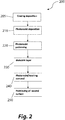
- a first preferred embodiment of the method according to the present invention comprises a preliminary deposition 205 of a coating film 333 on a first surface 334 of a substrate 330.
- This coating thin film 333 induces specific optical and electronic properties to the substrate 330. For example, alkali metals reduce the work function of a substrate and noble metals increase the optical reflectance of a substrate. Moreover, the coating thin film may reduce the surface roughness of the substrate. Then a photoresist deposition 210 of a thin positive photoresist film 335 on the coating film 333 is performed. In other embodiments of the method according to the invention, a deposition step of a thin negative photoresist film is performed.
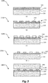
- the photoresist deposition 210 allows obtaining a substrate/coating film/photoresist film system 3000 shown in the cross-section of Figure 3(a) .
- the method includes the deposition 210 of the thin photoresist film 335 directly onto a first surface 334 of a substrate 330 without the preliminary deposition 205 of a coating film, thus obtaining a substrate/photoresist film system.
- the techniques of both preliminary deposition 205 of a coating film and photoresist deposition 210 are selected from the group consisting of spin coating, dip coating, roller coating, curtain coating, extrusion coating, meniscus coating, spray casting, silk screen printing, sputtering, thermal evaporation, electron-beam evaporation, pulsed-laser deposition, galvanic growth, electrophoresis, chemical vapour deposition.
- Substrate 330 comprises metallic materials, selected from the group consisting of refractory metals, noble metals, aluminium, nickel, chromium, or alternatively semiconductor or insulator materials, selected from the group consisting of silicon, germanium, gallium arsenide, gallium nitride, aluminium nitride, boron nitride, III-V in general and their ternary or quaternary compounds, diamond.
- Photoresist thickness has to be larger than the height of the DMSs to be obtained.
- the photoresist film 335 is then patterned 220 by optical lithography resulting in a photoresist pattern 339 corresponding to the pattern of the exposed areas 336 of photoresist film 335 (or to the pattern of unexposed areas in case of deposition of a negative photoresist film). Therefore, a substrate/coating film/photoresist pattern system 3100 is obtained and it is schematically shown in the cross-section of Figure 3(b) .
- opaque material master films e.g. chromium
- transparent (e.g. quartz) freestanding photomasks not shown in the Figures, were specifically designed and fabricated.
- the geometry is then transferred by using a lithographic contact, proximity or projection procedure, performed by illuminating the mask with optical radiation (e.g. UV), or direct writing such as in the case of laser writing or electron beam lithography or scanning probe lithography.
- optical radiation e.g. UV
- the optical lithographic procedure involves the use of a mask aligner in soft-contact, proximity or projection mode.
- the sample coated with the photoresist film 335 (on which the photomask is positioned) is exposed to optical radiation.
- the exposure duration time has to ensure the complete photoreaction of the exposed areas 336 of photoresist film 335.
- Photoresist is finally dipped in a dedicated chemical solution (developer), which removes unexposed areas of photoresist in case of a positive photoresist (or exposed areas in case of a negative photoresist).
- a dedicated chemical solution developer
- the photoresist film 335 is directly patterned by different pattering techniques selected from the group consisting of direct imprinting, direct laser writing, electron beam lithography, scanning probe lithography for higher resolution in the nanometre range.
- the substrate/coating film/photoresist film system 3000 is soft baked at temperatures ranging from 30 to 200 °C, preferably at 100 °C, for a time ranging from 1 to 3600 s, preferably 60s, in order to facilitate the evaporation of residual solvents present in the photoresist film 335.
- solvents may indeed contaminate the transparent photomask, or cause adhesions between the mask and the substrate surface on which the photoresist was deposited.
- the next step of the first preferred embodiment of method is a dielectric deposition 230 of a layer of dielectric material on the photoresist pattern 339 by sputtering technique.
- the dielectric deposition is performed by different additive deposition techniques such as thermal evaporation, electron-beam evaporation, pulsed-laser deposition, galvanic growth, electrophoresis, chemical vapour deposition.
- the dielectric film is selected among highly electrical resistive and poorly thermal conductive, thermally resistant materials at high temperatures, such as (but not limited to) aluminium oxide (alumina, Al 2 O 3 ), zirconium oxide (zirconia, ZrO 2 ), silicon oxide (SiO 2 ), boron nitride.
- the RF plasma produced by a magnetron sputtering deposits dielectric materials by a reactive deposition procedure using metal targets and oxygen.
- the dielectric deposition 230 of a layer of dielectric material can also be carried out by a direct procedure, therefore using dielectric oxide targets and inert gases (e.g. Argon), but, in this case, there is a drastic reduction in the deposition rate.
- the yield of dielectric deposition 230 is a dielectric layer 349 that is conformal to the underneath substrate/coating film/photoresist pattern.
- the dielectric layer 349 comprises a first dielectric pattern corresponding to the exposed areas 336 of photoresist (or unexposed areas in case of a negative photoresist), i.e.
- the photoresist pattern 339 and a second dielectric pattern 347 corresponding to the unexposed areas of photoresist (or exposed areas in case of a negative photoresist).
- the second dielectric pattern 347 is on the areas of the substrate 350 that are not occupied by (i.e. that are free of) the photoresist. Therefore, the second dielectric pattern 347 has been directly deposited on the coated first surface 334 of the substrate 330.
- a substrate/coating film/photoresist pattern/dielectric layer system 3200 is then obtained and it is schematically shown in the cross-section of Figure 3(c) .
- the next step of the method is a removal step 240 of the photoresist pattern 339 and consequently of the first dielectric pattern deposited on it.
- the array of DMSs is obtained according to the geometry defined during the photoresist patterning 220.
- the photoresist is removed by rinsing the substrate/photoresist pattern/dielectric layer system 3200 in removers specific for the used photoresist.
- common solvents such as acetone or dimethylsulfoxide can be used. Dielectric material deposited on the patterned resist (i.e. the first dielectric pattern) is washed away, whereas the dielectric material deposited on the substrate (i.e. the second dielectric pattern 347) remains unaltered, forming the array of DMSs.
- each single structure of the unaltered second dielectric pattern 347 correspond to a single DMS forming the array of DMS.
- a substrate/coating film/DMS array system 3300 is obtained and it is schematically shown in the cross-section of Figure 3(d) .
- a second surface 364 of a body 360 is then positioned 250 upon the array of DMSs, establishing a fixed distance from the substrate first surface 334 that is equal to the thickness of the array of DMSs.
- the final substrate/coating film/DMS array/body system 3400 is obtained and it is schematically shown in the cross-section of Figure 3(e) .
- the second surface 364 has a roughness that is lower than the height of the DMSs.
- the height of the DMS structures can range from few nanometres to 50 ⁇ m, optionally from few nanometres to 1 ⁇ m for thermo-tunnel diodes and from 0.5 ⁇ m to 50 ⁇ m for the thermionic energy converters.
- Typical lateral size of a single DMS structure ranges from few nanometres to 100 ⁇ m.
- An array or any geometrical arrangement of DMS structures can be as large as the substrate size.
- the shape of the single DMS structure is not limited to a single type, but the preferred embodiment is a cone or pyramid with the base in contact with the substrate, or truncated cone or prism or cylinder optionally hollowed to reduce contact area with the hot component, thus to reduce the thermal conduction mechanism, more preferably with features smaller than 10 nm in order to significantly reduce the thermal conductivity as described in " Ultralow thermal conductivity and mechanical resilience of architected nanolattices" by Rob Jagt, University of Groningen, May 2017 .
- a second preferred embodiment of the method according to the present invention is described.
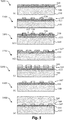
- This second preferred embodiment is similar to the first one, but comprises an additional deposition step 421 of a sacrificial layer on the photoresist pattern 539 of the substrate/coating film/photoresist pattern system 5100 (shown in Figure 5(b) ) and then an additional lift-off step 422 of the photoresist pattern 539.
- the additional steps 421 and 422 are performed after the photoresist patterning 420 and before the dielectric deposition 430 of the dielectric layer.
- the sacrificial layer 559 comprises materials such as metals, semiconductors, insulators or other polymers and it is conformal to the underneath photoresist pattern 539.
- the sacrificial layer comprises a first sacrificial pattern 556 corresponding to the exposed areas 536 of photoresist (or unexposed areas in case of a negative photoresist), i.e. the photoresist pattern 539, and a second sacrificial pattern 557 corresponding to the unexposed areas of photoresist in case of a positive photoresist (or exposed areas in case of a negative photoresist). Therefore, a substrate/coating film/photoresist pattern/sacrificial layer system 5101 is obtained and it is schematically shown in the cross-section of Figure 5(b1) .
- the lift-off step 422 is applied to the photoresist pattern 539, resulting in the removal of the first sacrificial pattern 556. Therefore, a substrate/coating film/second sacrificial pattern system 5102 is obtained and it is schematically shown in the cross-section of Figure 5(b2) .
- These additional steps 421 and 422 are performed to allow a larger versatility in the DMS fabrication: the sacrificial layer can be more resistant to the DMS deposition temperature or inert to the deposition atmosphere. A requirement is that the sacrificial layer material can be etched selectively with respect to the DMS material.
- photoresist patterning 420 is made by using a mask reporting an inverted pattern with respect to the mask used for photoresist patterning 220.
- photoresist patterning 420 can be made by using the same mask used for photoresist patterning 220, but making sure to use an inverted photoresist.
- the additional deposition technique is selected form the group consisting of spin coating, dip coating, roller coating, curtain coating, extrusion coating, meniscus coating, spray casting, silk screen printing, sputtering, thermal evaporation, electron-beam evaporation, pulsed-laser deposition, galvanic growth, electrophoresis, chemical vapour deposition.
- the subsequent steps of this second preferred embodiment are those already described above, i.e.
- dielectric material is deposited 430 on the second sacrificial pattern 557 obtaining a substrate/second sacrificial pattern/dielectric layer system 5200 ( Figure 5(c) ). Then the second sacrificial pattern 557 is removed by rinsing the substrate/second sacrificial pattern/dielectric layer system 5200 in removers, obtaining a substrate/coating film/DMS array system 5300 ( Figure 5(d) ). Finally, a second surface 564 of a body 560 is positioned 450 upon the array of DMSs, obtaining a final substrate/coating film/DMS array/body system 5400 schematically shown in the cross-section of Figure 5(e) . The second surface 564 has a roughness that is lower than the height of the DMSs.
- the dielectric deposition 230, 430 of a dielectric material layer 349, 549 is carried out by a sputtering apparatus 100 sketched in Figure 6 , as described hereafter.
- the sputtering apparatus 100 comprises a chamber 1 equipped with a pumping system (not shown in Figure 6 ) that guarantees a vacuum level lower than 10 -1 mbar, preferably lower than 10 -6 mbar, a magnetron source system 3, a first gas inlet 2 for a reactive gas flow close to a target 4, and a second gas inlet 5 for an oxygen flow close to a sample holder 10 housing a substrate 11 (i.e. the substrate/photoresist pattern system 310) on which the dielectric material has to be deposited.
- Two gas flow meters (not shown) are mounted on the gas inlets, allowing for a control of the reactive gas and oxygen flows.
- the sputtering apparatus 100 comprises a bias voltage control system (not shown), and a shutter 12 positioned over the target 4.
- the sputtering apparatus further comprises a thermocouple 6, for example but not limited to a type K, aimed at monitoring the process temperature T of the substrate 11 and, optionally, a high precision quartz microbalance 9 for measuring the deposition rate R and providing at the same time information on the oxidation process (when oxygen reacts with aluminium, the deposition rate reaches a steady state condition).
- a control unit 7 allows for a real-time monitoring and adjusting of the deposition parameters of the dielectric layer 50 on the substrate 11.
- sputtering technique guarantees the deposition of dielectric material on surfaces at relatively low temperatures (even ⁇ 100 °C) making possible to treat substrates that could be subject to damage if subjected to higher temperatures.
- different deposition techniques can be exploited, such as electron-beam (e-beam) evaporation, working at even lower temperatures, as well as thermal evaporation, pulsed-laser deposition, galvanic growth, electrophoresis, chemical vapour deposition.
- the deposition 230 of the dielectric layer by the sputtering system 100 is carried out according to the following steps:
- AZ 4533 (Microchemicals GmbH) is a positive near-UV photoresist for thin (up to 3 ⁇ m) surface coatings. After spin-coating, the sample is soft baked at 100 °C for 60 minutes, then the customized quartz photomask is positioned on the spin-coated samples. Then the sample+mask system is exposed to an UV radiation (i-line, 365 nm wavelength) using a 350 W mercury UV lamp (Osram HBO 350 W/S9). Time of exposure is 90 s. Finally, the sample is developed by using the developer AZ 826 MIF (Microchemicals GmbH) undiluted for 60 s. AZ 4533 has a maximum development rate of about 2 ⁇ m/min after exposition to a i-line intensity of 8.5 mW/cm 2 , typical of 350 W lamps.
- the deposition of alumina layer by a RF sputtering is carried out by means of an aluminium target and using oxygen as reactive gas.
- the process is strictly dependent on the base pressure, the partial pressures of the gases, the concentrations of aluminium and oxygen, as well as the ratio between them.
- the substrate is positioned inside the chamber, where it is expected that a pressure of 5x10 -6 mbar or less has been reached.
- the argon flow is set to a fixed value of 30 sccm and, keeping the shutter closed, a cleaning procedure of the target is carried out by pre-sputtering at 250 W power. After 15 minutes, the shutter is opened and the oxygen flow is set to values in the range 2.0-3.6 sccm.
- the magnetron source is powered at 180 - 230 W, high enough to guarantee a good sputtering yield of the aluminum target at a temperature lower than 100 °C.
- the process begins at an operating pressure in the range of 2.2 - 2.4x10 -3 mbar, the temperature is kept between 80 and 90 °C and the deposition rate is kept in the range 0.8-1 ⁇ /s.
- Figure 7 shows SEM images of an array of 5 ⁇ m diameter cup-shaped DMSs fabricated by the first preferred embodiment of the invention. This geometrical structure offers the advantage of further reducing the contact area between the two surfaces to be separated.
Landscapes
- Physical Vapour Deposition (AREA)
Abstract
Method for fabricating dielectric micro-spacers, DMSs, comprising the following steps:A. performing a photoresist deposition of a thin photoresist film on a surface of a substrate, the substrate being a metal, or a semiconductor or an insulator;B. patterning the photoresist film for obtaining a photoresist patter;C. performing a dielectric deposition of a dielectric layer by additive deposition techniques, the dielectric layer comprising a first dielectric pattern conformal to the photoresist pattern and a second dielectric pattern corresponding to areas of the first surface that are not occupied by the photoresist pattern, the dielectric layer being highly electrical resistive and poorly thermal conductive, having an electrical resistivity ranging from 10<sup>2</sup>Ω cm to 10<sup>18</sup>Ω cm and a thermal conductivity ranging from 10<sup>-3</sup>W/(cm K) to 10 W/(cm K).D. removing the photoresist pattern, whereby the first dielectric pattern deposited on the photoresist pattern is removed and the second dielectric pattern remaining unaltered and forming an array of DMSs.
Description
- The project leading to this application, that has been maintained confidential and has not been publicly disclosed so far, has received funding from the European Union's Horizon 2020 research and innovation programme under grant agreement No 754568.
- The present invention relates to a method for fabricating dielectric micro-spacers, DMSs, able to physically separate two surfaces at the micrometre scale and to ensure both a thermal and electrical separation between such surfaces maintaining their mechanical and functional properties at high temperature and in harsh environment. The method of the present invention is able to operate in a controlled, versatile, efficient, reliable, simple, and cost-effective way.
- A lot of devices belonging to a wide range of technological fields need to establish a fixed distance between two surfaces while ensuring thermal and/or electric insulation between them, as described hereinafter.
- For example, thermionic devices for energy conversion, TECs, operate as thermal vacuum diodes, and require very high operating temperatures (> 600 °C), whereas in case of photon-enhanced TECs the operating temperatures are lower (> 80 °C). In many cases, TECs are suitable for operation in extremely hot environments, such as nuclear reactors, propulsion systems in spacecrafts, solar concentrating systems, combustion chambers in petrol and/or air engines, or industrial furnaces, where they can be successfully employed as thermal energy recovery systems. The development of a spacer able to maintain a gap between the electrodes of few micrometres is a primary condition for the efficiency of a vacuum diode. The optimal gap value mainly depends on the TEC hot cathode operating temperature, but gaps larger than few micrometres induce a strong reduction of the established current between the electrodes, and consequently of the overall efficiency of the conversion module. Conversely, a gap between cathode and anode narrower than the optimal one is not desirable since it may cause anode overheating owing to near-field effects, resulting anyway in a conversion efficiency drop-off. Up to now, a widespread application of TECs was severely limited exactly because of the absence of a similar technology, substituted in a palliative way by the use of caesium vapours, which are toxic and lead to a significant reduction of efficiency, and magnetic fields, usually associated to the use of large magnets hampering down-scalable systems.
- In the field of microelectronics, lumped elements for RF and microwave circuits technology make large use of air-bridges and dielectric crossovers. The primary purpose of air-bridges and dielectric crossovers is to provide a cross-connection for two non-connecting printed transmission-line sections as shown in
Figure 1 . They are also commonly employed in transistors (e.g. to create a non-connecting crossover between a multiple source and gate, or emitter and base), electrodes, spiral inductors, transformers, metal-insulator-metal capacitors (to improve the breakdown voltage), and other RF and microwave circuits. Air-bridges and dielectric crossovers are also used to reduce the parasitic capacitance between the conductors and the ground plane in MMICs (i.e. Monolithic Microwave Integrated Circuits), thus increasing the maximum operating frequency of the devices. Air-bridges use air as the dielectric between the two conductors, whereas dielectric crossovers employ a layer of low dielectric constant material, such as polyimide or benzocyclobutene (BCB). Both air-bridges and dielectric crossovers have their own advantages and drawbacks: - Air-bridges. Being the primary function of air-bridges and dielectric crossovers to provide a perfect electrical insulation between two transmission lines (
Line 1 andLine 2 inFigure 1a ), air-bridges are undoubtedly preferable to dielectric crossovers, obviously because air has the lowest dielectric constant (approximatively equal to the vacuum one). On the other hand, air-bridges require very complex technological steps for their fabrication (e.g. prolonged chemical etching to "empty" the volume betweenLine 1 andLine 2 ofFigure 1a ), which result in a non-optimal process yield. Furthermore, the mechanical stability of the structure poses a constraint on the maximum length of the bridge: air-bridge collapse is observed rather frequently, further affecting the process yield. - Dielectric crossovers. The advantages of crossovers if compared to air-bridges are a simpler fabrication technology (mostly because there's no need to "empty" the inter-line space) and, obviously, a significantly better mechanical stability, acting the dielectric film also as a mechanical support for the overhead part of
Line 1 ofFigure 1b . However, low dielectric constant materials (such as polyimides and BCB) are only partially suitable to work in harsh environments: indeed, whilst the high operating temperature is not an issue (polyimides work well up to 250 - 300°C), radiation hardness is very poor. For example, electric conductivity of polyimide has been recently found to increase dramatically (several orders of magnitude) with increased electron exposure (Cooper et al., "Effects of Radiation Damage on Polyimide Resistivity", Journal of Spacecraft and Rockets, Vol. 54, No. 2 (2017), pp. 343-348). - Thermo-tunnel diodes are innovative devices for thermal energy recovery, and can be efficiently exploited in every field of application in which intermediate operating temperatures (<300 °C) are concerned, i.e. not high enough to ensure an efficient performance of pure thermionic devices. This is the case, for example, of all the automotive systems excluding the components of the exhaust system (e.g. engine compartment and transmission, wheel-ABS sensors, etc.), where temperatures as high as 800 °C can be reached. By coating the radiator with thermo-tunnel diodes it would be possible to double the engine's efficiency, because it's possible to eliminate the pumping, friction and incomplete fuel combustion loss. In its simplest form, a thermo-tunnel diode consists of two electrodes with a spacing of only a few nanometers, such that electrons are able to tunnel from one electrode to the other. However, because of the extremely narrow inter-electrode space, the two electrodes will get very likely into contact due to thermal expansion of metals at even moderate temperatures, causing a short-circuit and consequently a device failure. This is the reason why thermo-tunnel diodes, despite their very high potential, are still at a prototype level, and have not yet been developed on a large scale.
- Most of the above mentioned drawbacks and disadvantages are overcome by an array of dielectric solid microspacers that keeps two surfaces well separated but very close to each other avoiding any point of contact, and ensuring that the volume of space between the surfaces (namely the inter-surface gap) is occupied by a solid material as few as possible, which means that the inter-surface gap should be almost entirely an empty space (i.e. a vacuum or a gas-filled space). Such array of DMSs has to be mechanically, chemically, and physically stable in a broad range of high temperatures, from room temperature to values even >500 °C, and in harsh environments such as for example space and nuclear reactors, for maintaining the fixed distance between the two surfaces to be separated and ensuring the thermal and electric insulation between them.
- In fact, the exploitation of DMSs in thermionic devices for energy conversion improves their efficiency and avoids using caesium vapours and magnetic fields, thus improving environmental sustainability and scalability of devices. In the automotive field, among the different powertrain components, those related to the combustion chamber and the exhaust systems may reach significantly high temperatures (500 °C - 800 °C), enabling the possibility of applying thermionic devices exploiting DMSs. The integration of arrays of thermionic energy converters equipped with DMSs, able to convert the exhaust heat into electric power, can be successfully used to create an additional energy source (for example supporting the car battery or supplying low-power devices, such as LEDs, actuators, or even the MEMS sensors themselves). In fact, it is possible to compensate the energy losses of a thermal engine deriving from pumping, friction and incomplete fuel combustion by thermionic diodes that generate an equivalent power amount. Coating the radiator and the exhaust system with them could allow for doubling the engine efficiency.
- Moreover, DMSs may represent the optimal solution for lumped elements for RF and microwave circuits, because they represent the perfect trade-off between air-bridges and dielectric crossovers, retaining all the advantages of the two technologies and removing their drawbacks:
- DMSs ensure approximatively the same dielectric behaviour of air-bridges (being the inter-line space only minimally occupied by the micro-spacers), but constraints on the maximum length of the bridge are removed, because DMSs act as bridge piers, allowing for a practically unlimited length without risk of collapse. Also, the fabrication process is slightly more simple and reliable than air-bridges, resulting in a better process yield.
- DMSs can be made up of are radiation-hard materials, such as for example alumina and zirconia. This overcomes the limitations of conventional dielectric crossovers in harsh environments, where a significant amount of ionizing radiation may be present.
- Also, DMSs may represent a turning point for thermo-tunnel diode technology, avoiding any kind of short circuit, and allowing at the same time an efficient electron tunnelling by maximizing the cathode free surface. An inter-electrode space of a few nanometres, which is a distance about two orders of magnitude smaller than the case of a thermionic energy converter, represents a challenge for DMS technology itself. However, the technological improvements disclosed in the present invention below, may overcome in the short term this limitation, mostly through the employment of planarization techniques such as CMP (Chemical Mechanical Planarization).
- Several documents of prior art disclose methods for realizing micrometre-scale spacers whose aim is either thermally or electrically insulate two surfaces kept at fixed distance. However such methods are not suitable to obtain spacers for more than one purpose per time.
- Even more critical is the fact that most of these methods have a top-down approach performed by a subtractive manufacturing, by first depositing a continuous film of the spacing material onto the surface of a substrate, and then fabricating the desired pattern, i.e the array of microspacers, by selective removal of the deposited material. The selective removal usually involves wet or dry etching performed by acids or aggressive ionized plasmas (e.g. using techniques as semi-isotropic dry plasma etching, reactive ion etching, or sputter etching), thus damaging some kind of substrates such as metallic ones. Therefore only substrates that do not undergo deterioration during the removal steps of the method can be used. In particular, prior art documents only disclose methods for fabricating micro-spacers onto semiconductor substrates.
- It is an object of this invention to overcome the disadvantages described above, allowing for the fabrication of solid dielectric micro-spacers on different types of substrates, such as metals, semiconductors, or insulators, ensuring a mechanical separation and a thermal and electrical insulation between the substrate surface and another surface facing it at a distance of few micrometres.
- It is specific subject-matter of the present invention a method for fabricating an array of DMSs as described in the
independent claim 1. - Further embodiments of the method according to the invention are described in the dependent claims.
- It is antoher specific subject-matter of the present invention a device as described in the
independent claim 10. - Further embodiment of the device according to the invention is described in the
dependent claim 11. - It is antoher specific subject-matter of the present invention a device as described in the
independent claim 12. - Further embodiment of the device according to the invention is described in the dependent claim 13.
- The advantages offered by the method according to the invention with respect to the prior art solutions are numerous and significant.
- First, the method is based on a bottom-up approach performed by an addictive manufacturing, i.e. DMSs arrays are fabricated by depositing a conformal film of the dielectric material onto the patterned substrate, then lifting-off the masking layer. This, advantageously, allows for the use of a wider selection of substrates (e.g metallic substrates) with respect to the state-of-the-art methods. Another advantage is that the method of the present invention allows obtaining thermal and electrical barriers between two surfaces kept at a fixed distance that can be used in devices in a wide range of different technological applications. Furthermore, the method fabricates thermal and electrical dielectric (e.g. alumina, zirconia) barriers that are mechanically and chemically-physically stable at high temperature and in harsh environments. Finally, it's worth recalling that the method for fabricating DMSs is scalable, cost-effective, can be implemented by limited-size deposition systems, and allows for an accurate and real-time control of all the fabrication parameters.
- The present invention will be described, by way of illustration, but not by way of limitation, according to its preferred embodiments, with particular reference to the Figures of the accompanying drawings, in which:
-
Figure 1 shows air-bridges (a) and dielectric crossovers (b) currently employed in the technology of lumped elements for RF and microwave integrated circuits; -
Figure 2 shows a block diagram of a first preferred embodiment of the method for fabricating an array of DMSs according to the invention; -
Figures 3(a)-3(e) schematically illustrate cross-section views of sequential stages of the method for fabricating an array of DMSs ofFigure 2 using of a positive photoresist film; -
Figure 4 shows a block diagram of a second preferred embodiment of the method for fabricating an array of DMSs according to the invention; -
Figures 5(a)-5(g) schematically illustrate cross-section views of sequential stages of the method for fabricating an array of DMSs ofFigure 4 ; -
Figure 6 shows a sketch of a preferred embodiment of a sputtering apparatus for carrying out the method for fabricating an array of DMSs ofFigures 3 ; -
Figures 7(a)-7(b) show scanning electron micrographs (SEM) of an array of DMSs obtained by carrying out a second embodiment of the invention. - In the Figures, identical reference numerals will be used for alike elements.
- With reference to
Figures 2 and3 , a first preferred embodiment of the method according to the present invention is described. It comprises apreliminary deposition 205 of acoating film 333 on afirst surface 334 of asubstrate 330. This coatingthin film 333 induces specific optical and electronic properties to thesubstrate 330. For example, alkali metals reduce the work function of a substrate and noble metals increase the optical reflectance of a substrate. Moreover, the coating thin film may reduce the surface roughness of the substrate. Then aphotoresist deposition 210 of a thinpositive photoresist film 335 on thecoating film 333 is performed. In other embodiments of the method according to the invention, a deposition step of a thin negative photoresist film is performed. Thephotoresist deposition 210 allows obtaining a substrate/coating film/photoresist film system 3000 shown in the cross-section ofFigure 3(a) . In other embodiments of the method according to this invention, the method includes thedeposition 210 of thethin photoresist film 335 directly onto afirst surface 334 of asubstrate 330 without thepreliminary deposition 205 of a coating film, thus obtaining a substrate/photoresist film system. The techniques of bothpreliminary deposition 205 of a coating film andphotoresist deposition 210 are selected from the group consisting of spin coating, dip coating, roller coating, curtain coating, extrusion coating, meniscus coating, spray casting, silk screen printing, sputtering, thermal evaporation, electron-beam evaporation, pulsed-laser deposition, galvanic growth, electrophoresis, chemical vapour deposition.Substrate 330 comprises metallic materials, selected from the group consisting of refractory metals, noble metals, aluminium, nickel, chromium, or alternatively semiconductor or insulator materials, selected from the group consisting of silicon, germanium, gallium arsenide, gallium nitride, aluminium nitride, boron nitride, III-V in general and their ternary or quaternary compounds, diamond. Photoresist thickness has to be larger than the height of the DMSs to be obtained. Thephotoresist film 335 is then patterned 220 by optical lithography resulting in aphotoresist pattern 339 corresponding to the pattern of the exposed areas 336 of photoresist film 335 (or to the pattern of unexposed areas in case of deposition of a negative photoresist film). Therefore, a substrate/coating film/photoresist pattern system 3100 is obtained and it is schematically shown in the cross-section ofFigure 3(b) . In order to transfer selected geometries on the photoresist, opaque material master films (e.g. chromium) developed on transparent (e.g. quartz) freestanding photomasks, not shown in the Figures, were specifically designed and fabricated. The geometry is then transferred by using a lithographic contact, proximity or projection procedure, performed by illuminating the mask with optical radiation (e.g. UV), or direct writing such as in the case of laser writing or electron beam lithography or scanning probe lithography. The optical lithographic procedure involves the use of a mask aligner in soft-contact, proximity or projection mode. The sample coated with the photoresist film 335 (on which the photomask is positioned) is exposed to optical radiation. The exposure duration time has to ensure the complete photoreaction of the exposed areas 336 ofphotoresist film 335. Photoresist is finally dipped in a dedicated chemical solution (developer), which removes unexposed areas of photoresist in case of a positive photoresist (or exposed areas in case of a negative photoresist). In other embodiments of the method according to this invention, thephotoresist film 335 is directly patterned by different pattering techniques selected from the group consisting of direct imprinting, direct laser writing, electron beam lithography, scanning probe lithography for higher resolution in the nanometre range. - Optionally, after the
photoresist deposition 210, the substrate/coating film/photoresist film system 3000 is soft baked at temperatures ranging from 30 to 200 °C, preferably at 100 °C, for a time ranging from 1 to 3600 s, preferably 60s, in order to facilitate the evaporation of residual solvents present in thephotoresist film 335. Such solvents may indeed contaminate the transparent photomask, or cause adhesions between the mask and the substrate surface on which the photoresist was deposited.
The next step of the first preferred embodiment of method is adielectric deposition 230 of a layer of dielectric material on thephotoresist pattern 339 by sputtering technique. In other embodiments of the method according to this invention, the dielectric deposition is performed by different additive deposition techniques such as thermal evaporation, electron-beam evaporation, pulsed-laser deposition, galvanic growth, electrophoresis, chemical vapour deposition. The dielectric film is selected among highly electrical resistive and poorly thermal conductive, thermally resistant materials at high temperatures, such as (but not limited to) aluminium oxide (alumina, Al2O3), zirconium oxide (zirconia, ZrO2), silicon oxide (SiO2), boron nitride. In the first preferred embodiments of the invention, the RF plasma produced by a magnetron sputtering deposits dielectric materials by a reactive deposition procedure using metal targets and oxygen. Alternatively, thedielectric deposition 230 of a layer of dielectric material can also be carried out by a direct procedure, therefore using dielectric oxide targets and inert gases (e.g. Argon), but, in this case, there is a drastic reduction in the deposition rate. The yield ofdielectric deposition 230 is adielectric layer 349 that is conformal to the underneath substrate/coating film/photoresist pattern. Thedielectric layer 349 comprises a first dielectric pattern corresponding to the exposed areas 336 of photoresist (or unexposed areas in case of a negative photoresist), i.e. thephotoresist pattern 339, and a seconddielectric pattern 347 corresponding to the unexposed areas of photoresist (or exposed areas in case of a negative photoresist). In other words, the seconddielectric pattern 347 is on the areas of the substrate 350 that are not occupied by (i.e. that are free of) the photoresist. Therefore, the seconddielectric pattern 347 has been directly deposited on the coatedfirst surface 334 of thesubstrate 330. A substrate/coating film/photoresist pattern/dielectric layer system 3200 is then obtained and it is schematically shown in the cross-section ofFigure 3(c) . The next step of the method is aremoval step 240 of thephotoresist pattern 339 and consequently of the first dielectric pattern deposited on it. In this way, the array of DMSs is obtained according to the geometry defined during thephotoresist patterning 220. The photoresist is removed by rinsing the substrate/photoresist pattern/dielectric layer system 3200 in removers specific for the used photoresist. In other embodiments of the invention, common solvents such as acetone or dimethylsulfoxide can be used. Dielectric material deposited on the patterned resist (i.e. the first dielectric pattern) is washed away, whereas the dielectric material deposited on the substrate (i.e. the second dielectric pattern 347) remains unaltered, forming the array of DMSs. In other words, each single structure of the unaltered seconddielectric pattern 347 correspond to a single DMS forming the array of DMS. A substrate/coating film/DMS array system 3300 is obtained and it is schematically shown in the cross-section ofFigure 3(d) . Asecond surface 364 of abody 360 is then positioned 250 upon the array of DMSs, establishing a fixed distance from the substratefirst surface 334 that is equal to the thickness of the array of DMSs. The final substrate/coating film/DMS array/body system 3400 is obtained and it is schematically shown in the cross-section ofFigure 3(e) . Thesecond surface 364 has a roughness that is lower than the height of the DMSs. - The height of the DMS structures can range from few nanometres to 50 µm, optionally from few nanometres to 1 µm for thermo-tunnel diodes and from 0.5 µm to 50 µm for the thermionic energy converters. Typical lateral size of a single DMS structure ranges from few nanometres to 100 µm. An array or any geometrical arrangement of DMS structures can be as large as the substrate size. The shape of the single DMS structure is not limited to a single type, but the preferred embodiment is a cone or pyramid with the base in contact with the substrate, or truncated cone or prism or cylinder optionally hollowed to reduce contact area with the hot component, thus to reduce the thermal conduction mechanism, more preferably with features smaller than 10 nm in order to significantly reduce the thermal conductivity as described in "Ultralow thermal conductivity and mechanical resilience of architected nanolattices" by Rob Jagt, University of Groningen, May 2017.
- With reference to
Figure 4 and5 , a second preferred embodiment of the method according to the present invention is described. This second preferred embodiment is similar to the first one, but comprises anadditional deposition step 421 of a sacrificial layer on thephotoresist pattern 539 of the substrate/coating film/photoresist pattern system 5100 (shown inFigure 5(b) ) and then an additional lift-off step 422 of thephotoresist pattern 539. Theadditional steps photoresist patterning 420 and before thedielectric deposition 430 of the dielectric layer. The sacrificial layer 559 comprises materials such as metals, semiconductors, insulators or other polymers and it is conformal to theunderneath photoresist pattern 539. The sacrificial layer comprises a firstsacrificial pattern 556 corresponding to the exposedareas 536 of photoresist (or unexposed areas in case of a negative photoresist), i.e. thephotoresist pattern 539, and a secondsacrificial pattern 557 corresponding to the unexposed areas of photoresist in case of a positive photoresist (or exposed areas in case of a negative photoresist). Therefore, a substrate/coating film/photoresist pattern/sacrificial layer system 5101 is obtained and it is schematically shown in the cross-section ofFigure 5(b1) . After that, the lift-off step 422 is applied to thephotoresist pattern 539, resulting in the removal of the firstsacrificial pattern 556. Therefore, a substrate/coating film/secondsacrificial pattern system 5102 is obtained and it is schematically shown in the cross-section ofFigure 5(b2) . Theseadditional steps photoresist patterning 420 is made by using a mask reporting an inverted pattern with respect to the mask used forphotoresist patterning 220. Alternatively,photoresist patterning 420 can be made by using the same mask used forphotoresist patterning 220, but making sure to use an inverted photoresist. The additional deposition technique is selected form the group consisting of spin coating, dip coating, roller coating, curtain coating, extrusion coating, meniscus coating, spray casting, silk screen printing, sputtering, thermal evaporation, electron-beam evaporation, pulsed-laser deposition, galvanic growth, electrophoresis, chemical vapour deposition. The subsequent steps of this second preferred embodiment are those already described above, i.e. dielectric material is deposited 430 on the secondsacrificial pattern 557 obtaining a substrate/second sacrificial pattern/dielectric layer system 5200 (Figure 5(c) ). Then the secondsacrificial pattern 557 is removed by rinsing the substrate/second sacrificial pattern/dielectric layer system 5200 in removers, obtaining a substrate/coating film/DMS array system 5300 (Figure 5(d) ). Finally, asecond surface 564 of abody 560 is positioned 450 upon the array of DMSs, obtaining a final substrate/coating film/DMS array/body system 5400 schematically shown in the cross-section ofFigure 5(e) . Thesecond surface 564 has a roughness that is lower than the height of the DMSs. - In a preferred embodiment of the method, the
dielectric deposition dielectric material layer sputtering apparatus 100 sketched inFigure 6 , as described hereafter. - The
sputtering apparatus 100 comprises achamber 1 equipped with a pumping system (not shown inFigure 6 ) that guarantees a vacuum level lower than 10-1 mbar, preferably lower than 10-6 mbar, amagnetron source system 3, afirst gas inlet 2 for a reactive gas flow close to atarget 4, and asecond gas inlet 5 for an oxygen flow close to asample holder 10 housing a substrate 11 (i.e. the substrate/photoresist pattern system 310) on which the dielectric material has to be deposited. Two gas flow meters (not shown) are mounted on the gas inlets, allowing for a control of the reactive gas and oxygen flows. Thesputtering apparatus 100 comprises a bias voltage control system (not shown), and ashutter 12 positioned over thetarget 4. The sputtering apparatus further comprises athermocouple 6, for example but not limited to a type K, aimed at monitoring the process temperature T of thesubstrate 11 and, optionally, a highprecision quartz microbalance 9 for measuring the deposition rate R and providing at the same time information on the oxidation process (when oxygen reacts with aluminium, the deposition rate reaches a steady state condition). Acontrol unit 7 allows for a real-time monitoring and adjusting of the deposition parameters of thedielectric layer 50 on thesubstrate 11. - The use of sputtering technique guarantees the deposition of dielectric material on surfaces at relatively low temperatures (even <100 °C) making possible to treat substrates that could be subject to damage if subjected to higher temperatures. In another embodiment of the present invention, different deposition techniques can be exploited, such as electron-beam (e-beam) evaporation, working at even lower temperatures, as well as thermal evaporation, pulsed-laser deposition, galvanic growth, electrophoresis, chemical vapour deposition.
- In the preferred embodiment of the present invention, the
deposition 230 of the dielectric layer by thesputtering system 100 is carried out according to the following steps: - The
substrate 11 is first subjected to acid cleaning (e.g., with a buffered solution HF: H2O = 1: 100 to remove the native oxides). - Deposition chamber is evacuated until reaching the appropriate base pressure (1-2x10⁻⁶ mbar or less).
- The argon flow necessary to sputter the metal particles from the solid target is set to a value ranging from 1 to 1000 sccm (preferably 30 sccm).
- The power value on the magnetron source is set to a value high enough for an efficient sputtering yield, but not too high to avoid temperatures higher than 100 °C;
- Pre-sputtering is performed to remove possible native oxide layers from the target (maintaining the shutter closed in order to avoid deposition of sputtered atoms on the substrate);
- The flow of O2 (or other reactive gases, including air) is set to enable a the desired deposition rate, preferably in the range 1 - 10 Å/s. The operating pressure is set by a vacuum gate or valve that can be partially opened with a manual or electronic control.
- The stability of the deposition parameters, as well as of the operating temperature and pressure, is monitored for a few minutes to ensure a stable and deposition rate. The parameters that mostly influence the stoichiometric characteristics of the DMSs are the oxygen flow and the power supplied to the source. The experimental conditions are therefore varied by mainly acting on these two parameters.
- If necessary, the deposition parameters are adjusted to keep the deposition rate stable during the process; the rate can be controlled by reading the measured value from the quartz microbalance.
- Deposition on the substrate starts by opening the optional shutter.
- Optional shutter is closed when the deposited film has reached the desired thickness.
- Inventors implemented the first preferred embodiment of this invention in several experiments. A detailed description of the resist
deposition step layer deposition step photoresist removal step - AZ 4533 (Microchemicals GmbH) is a positive near-UV photoresist for thin (up to 3 µm) surface coatings. After spin-coating, the sample is soft baked at 100 °C for 60 minutes, then the customized quartz photomask is positioned on the spin-coated samples. Then the sample+mask system is exposed to an UV radiation (i-line, 365 nm wavelength) using a 350 W mercury UV lamp (Osram HBO 350 W/S9). Time of exposure is 90 s. Finally, the sample is developed by using the developer AZ 826 MIF (Microchemicals GmbH) undiluted for 60 s. AZ 4533 has a maximum development rate of about 2 µm/min after exposition to a i-line intensity of 8.5 mW/cm2, typical of 350 W lamps.
- The deposition of alumina layer by a RF sputtering is carried out by means of an aluminium target and using oxygen as reactive gas. The process is strictly dependent on the base pressure, the partial pressures of the gases, the concentrations of aluminium and oxygen, as well as the ratio between them. The substrate is positioned inside the chamber, where it is expected that a pressure of 5x10⁻⁶ mbar or less has been reached. The argon flow is set to a fixed value of 30 sccm and, keeping the shutter closed, a cleaning procedure of the target is carried out by pre-sputtering at 250 W power. After 15 minutes, the shutter is opened and the oxygen flow is set to values in the range 2.0-3.6 sccm. Note that the increase of oxygen flow causes a drastic reduction in the deposition rate (below 0.4 Å/s). Then, the magnetron source is powered at 180 - 230 W, high enough to guarantee a good sputtering yield of the aluminum target at a temperature lower than 100 °C. The process begins at an operating pressure in the range of 2.2 - 2.4x10⁻³ mbar, the temperature is kept between 80 and 90 °C and the deposition rate is kept in the range 0.8-1 Å/s.
- The deposition of a good quality stoichiometric zirconia layer is the same as the one described for alumina layer with the following differences:
- use of a zirconium target;
- higher Ar flow (40 sccm);
- wider range of operating pressures (2.0 - 3.0x10⁻³ mbar);
- wider range of deposition temperatures (65 - 100 °C);
- lower deposition rate (0.4 - 0.9 Å/s).
- The lift-off process is carried out by dipping the sample in undiluted AZ100 Remover at 60 °C for 5 minutes.
Figure 7 shows SEM images of an array of 5 µm diameter cup-shaped DMSs fabricated by the first preferred embodiment of the invention. This geometrical structure offers the advantage of further reducing the contact area between the two surfaces to be separated. - The preferred embodiments of this invention have been described, but it should be understood that those skilled in the art can make other variations and changes, without so departing from the scope of protection thereof, as defined by the attached claims.
Claims (13)
- Method for fabricating dielectric micro-spacers, DMSs, comprising the following steps:A. performing a photoresist deposition (210; 410) of a thin photoresist film (335; 535) on a surface (334; 534) of a substrate (330; 530), the substrate (330; 530) being a metal, or a semiconductor or an insulator;B. patterning (220; 420) the photoresist film (335; 535) for obtaining a photoresist patter (339; 539);C. performing a dielectric deposition (230; 430) of a dielectric layer (349; 549) by additive deposition techniques, the dielectric layer (349; 549) comprising a first dielectric pattern (346; 546) conformal to the photoresist pattern (349; 549) and a second dielectric pattern (347; 547) corresponding to areas of the first surface (334; 534) that are not occupied by the photoresist pattern (339; 539), the dielectric layer (349; 549) being highly electrical resistive and poorly thermal conductive, having an electrical resistivity ranging from 102 Ω cm to 1018 Ω cm and a thermal conductivity ranging from 10-3 W/(cm K) to 10 W/(cm K).D. removing (240; 440) the photoresist pattern (339; 539), whereby the first dielectric pattern (346; 546) deposited on the photoresist pattern (339; 539) is removed and the second dielectric pattern (347; 547) remaining unaltered and forming an array of DMSs.
- Method according to claim 1, wherein the substrate (330; 530) comprises metallic material selected from the group consisting of refractory metals, noble metals, aluminium, nickel, chromium, or alternatively semiconductor or insulator materials selected from the group consisting of silicon, germanium, gallium arsenide, gallium nitride, aluminium nitride, boron nitride, III-V in general and their ternary or quaternary compounds, diamond.
- Method according to claim 1 or 2, wherein the photoresist film (335; 535) has a thickness larger than a thickness of the dielectric layer (349; 549).
- Method according to any one of the preceding claims, comprising before step A the following step:A0. preliminary deposition (205; 405) of a coating film (333; 533) on the first surface (334; 534) configured to induce specific optical and electronic properties to the substrate (330; 530), wherein optionally the preliminary deposition is performed by a technique selected from the group consisting of spin coating, dip coating, roller coating, curtain coating, extrusion coating, meniscus coating, spray casting, silk screen printing, sputtering, thermal evaporation, electron-beam evaporation, pulsed-laser deposition, galvanic growth, electrophoresis, chemical vapour deposition.
- Method according to any one of the preceding claims, wherein step A is performed by a technique selected from the group consisting of spin coating, dip coating, roller coating, curtain coating, extrusion coating, meniscus coating, spray casting, silk screen printing, sputtering, thermal evaporation, electron-beam evaporation, pulsed-laser deposition, galvanic growth, electrophoresis, chemical vapour deposition.
- Method according to any one of the preceding claims, wherein step C is performed by means of a RF plasma produced by a magnetron sputtering depositing dielectric materials by a reactive deposition procedure using metal targets and oxygen or dielectric oxide targets and inert gases.
- Method according to any one of the preceding claims, wherein the thickness of the dielectric layer (349; 549) ranges from few nanometres to 50 µm and a lateral size of a structure of the second dielectric pattern (347; 547) ranges from few nanometres to 100 µm.
- Method according to any one of the preceding claims, wherein a shape of the single structure of the second dielectric pattern (347; 547) is selected form the group consisting of cone, truncated cone, pyramid, prism, cylinder, hollowed cylinder, with a base in contact with the substrate (330;530).
- Method according to any one of the preceding claims, comprising after step A the following step:E. positioning (250; 450) upon the array of DMSs a second surface 364 of a body 360, establishing a fixed distance from the first surface (334; 534).
- Device manufactured by the method of claim 9, configured to be used as thermo-tunnel diodes.
- Device according to claim 10, wherein each DMS has a height ranging from few nanometres to 1 µm.
- Device manufactured by the method of claim 9, configured to be used as thermionic energy converters.
- Device according to claim 12, wherein each DMS has a height ranging from 0.5 µm to 50 µm.
Priority Applications (1)
| Application Number | Priority Date | Filing Date | Title |
|---|---|---|---|
| EP18209581.0A EP3660884A1 (en) | 2018-11-30 | 2018-11-30 | Method for fabricating dielectric micro-spacers on different substrates |
Applications Claiming Priority (1)
| Application Number | Priority Date | Filing Date | Title |
|---|---|---|---|
| EP18209581.0A EP3660884A1 (en) | 2018-11-30 | 2018-11-30 | Method for fabricating dielectric micro-spacers on different substrates |
Publications (1)
| Publication Number | Publication Date |
|---|---|
| EP3660884A1 true EP3660884A1 (en) | 2020-06-03 |
Family
ID=64572124
Family Applications (1)
| Application Number | Title | Priority Date | Filing Date |
|---|---|---|---|
| EP18209581.0A Withdrawn EP3660884A1 (en) | 2018-11-30 | 2018-11-30 | Method for fabricating dielectric micro-spacers on different substrates |
Country Status (1)
| Country | Link |
|---|---|
| EP (1) | EP3660884A1 (en) |
Citations (3)
| Publication number | Priority date | Publication date | Assignee | Title |
|---|---|---|---|---|
| WO2007044517A1 (en) * | 2005-10-06 | 2007-04-19 | Borealis Technical Limited | Thermionic/thermotunneling thermo-electrical converter |
| EP3206060A1 (en) * | 2016-02-12 | 2017-08-16 | Viavi Solutions Inc. | Optical filter array |
| US20180202903A1 (en) * | 2015-08-10 | 2018-07-19 | Essenlix Corporation | Bio/chemical assay devices and methods for simplified steps, small samples, accelerated speed, and ease-of-use |
-
2018
- 2018-11-30 EP EP18209581.0A patent/EP3660884A1/en not_active Withdrawn
Patent Citations (3)
| Publication number | Priority date | Publication date | Assignee | Title |
|---|---|---|---|---|
| WO2007044517A1 (en) * | 2005-10-06 | 2007-04-19 | Borealis Technical Limited | Thermionic/thermotunneling thermo-electrical converter |
| US20180202903A1 (en) * | 2015-08-10 | 2018-07-19 | Essenlix Corporation | Bio/chemical assay devices and methods for simplified steps, small samples, accelerated speed, and ease-of-use |
| EP3206060A1 (en) * | 2016-02-12 | 2017-08-16 | Viavi Solutions Inc. | Optical filter array |
Non-Patent Citations (2)
| Title |
|---|
| COOPER ET AL.: "Effects of Radiation Damage on Polyimide Resistivity", JOURNAL OF SPACECRAFT AND ROCKETS, vol. 54, no. 2, 2017, pages 343 - 348 |
| ROB JAGT: "Ultralow thermal conductivity and mechanical resilience of architected nanolattices", May 2017, UNIVERSITY OF GRONINGEN |
Similar Documents
| Publication | Publication Date | Title |
|---|---|---|
| CN110663117B (en) | A kind of graphene field effect transistor and preparation method thereof | |
| US20150132548A1 (en) | Structures having graphene sets | |
| CN104701146B (en) | Graphene nano electronic device and preparation method thereof | |
| US11881539B2 (en) | Structure and method of advanced LCoS back-plane having highly reflective pixel via metallization | |
| TWI791328B (en) | Method of forming pixel isolation structure on semiconductor substrate and semiconductor structure | |
| US11586067B2 (en) | Structure and method of advanced LCoS back-plane having robust pixel via metallization | |
| US9688540B2 (en) | Segmented graphene growth on surfaces of a patterned substrate layer and devices thereof | |
| TW202034435A (en) | Carrier and its manufacturing method | |
| CN101459119B (en) | Method for forming contact hole | |
| WO2019212272A1 (en) | Resistive switching memory having resistive switching layer, manufactured by sputtering method, and manufacturing method therefor | |
| WO2013012195A2 (en) | Method for manufacturing substrate and method or manufacturing electronic device using same | |
| TWI881220B (en) | Metal oxide resist patterning with electrical field guided post-exposure bake | |
| US20230114700A1 (en) | Hard mask liftoff processes | |
| US20240087910A1 (en) | Methods of highly selective silicon oxide removal | |
| US20210305048A1 (en) | Methods to reduce microbridge defects in euv patterning for microelectronic workpieces | |
| CN116133495B (en) | Preparation method of carbon-based sensing chip | |
| JP3950628B2 (en) | Method for manufacturing a broad membrane mask | |
| US20250015141A1 (en) | Semiconductor device and formation method thereof | |
| US10607852B2 (en) | Selective nitride etching method for self-aligned multiple patterning | |
| WO2016077586A1 (en) | Fabrication of nanoscale vacuum grid and electrode structure with high aspect ratio dielectric spacers between the grid and electrode | |
| CN116487411A (en) | A strained two-dimensional semiconductor transistor and its preparation method | |
| JP2002299705A (en) | Fabrication method of small area tunnel junction | |
| KR102693356B1 (en) | Micro-patterning organic thin film transistor and manufacturing method thereof | |
| EP2985798B1 (en) | Method for manufacturing an organic electronic device | |
| US20230263075A1 (en) | High quality quantum computer components |
Legal Events
| Date | Code | Title | Description |
|---|---|---|---|
| PUAI | Public reference made under article 153(3) epc to a published international application that has entered the european phase |
Free format text: ORIGINAL CODE: 0009012 |
|
| STAA | Information on the status of an ep patent application or granted ep patent |
Free format text: STATUS: THE APPLICATION HAS BEEN PUBLISHED |
|
| AK | Designated contracting states |
Kind code of ref document: A1 Designated state(s): AL AT BE BG CH CY CZ DE DK EE ES FI FR GB GR HR HU IE IS IT LI LT LU LV MC MK MT NL NO PL PT RO RS SE SI SK SM TR |
|
| AX | Request for extension of the european patent |
Extension state: BA ME |
|
| STAA | Information on the status of an ep patent application or granted ep patent |
Free format text: STATUS: THE APPLICATION IS DEEMED TO BE WITHDRAWN |
|
| 18D | Application deemed to be withdrawn |
Effective date: 20201204 |