EP3657910A1 - Led lighting device and dimming control method therefor - Google Patents
Led lighting device and dimming control method therefor Download PDFInfo
- Publication number
- EP3657910A1 EP3657910A1 EP18835419.5A EP18835419A EP3657910A1 EP 3657910 A1 EP3657910 A1 EP 3657910A1 EP 18835419 A EP18835419 A EP 18835419A EP 3657910 A1 EP3657910 A1 EP 3657910A1
- Authority
- EP
- European Patent Office
- Prior art keywords
- control unit
- dimming
- signal
- voltage
- transformer
- Prior art date
- Legal status (The legal status is an assumption and is not a legal conclusion. Google has not performed a legal analysis and makes no representation as to the accuracy of the status listed.)
- Granted
Links
Images

Classifications
-
- H—ELECTRICITY
- H05—ELECTRIC TECHNIQUES NOT OTHERWISE PROVIDED FOR
- H05B—ELECTRIC HEATING; ELECTRIC LIGHT SOURCES NOT OTHERWISE PROVIDED FOR; CIRCUIT ARRANGEMENTS FOR ELECTRIC LIGHT SOURCES, IN GENERAL
- H05B45/00—Circuit arrangements for operating light-emitting diodes [LED]
- H05B45/30—Driver circuits
- H05B45/37—Converter circuits
- H05B45/3725—Switched mode power supply [SMPS]
- H05B45/385—Switched mode power supply [SMPS] using flyback topology
-
- H—ELECTRICITY
- H05—ELECTRIC TECHNIQUES NOT OTHERWISE PROVIDED FOR
- H05B—ELECTRIC HEATING; ELECTRIC LIGHT SOURCES NOT OTHERWISE PROVIDED FOR; CIRCUIT ARRANGEMENTS FOR ELECTRIC LIGHT SOURCES, IN GENERAL
- H05B45/00—Circuit arrangements for operating light-emitting diodes [LED]
-
- H—ELECTRICITY
- H05—ELECTRIC TECHNIQUES NOT OTHERWISE PROVIDED FOR
- H05B—ELECTRIC HEATING; ELECTRIC LIGHT SOURCES NOT OTHERWISE PROVIDED FOR; CIRCUIT ARRANGEMENTS FOR ELECTRIC LIGHT SOURCES, IN GENERAL
- H05B45/00—Circuit arrangements for operating light-emitting diodes [LED]
- H05B45/10—Controlling the intensity of the light
-
- H—ELECTRICITY
- H05—ELECTRIC TECHNIQUES NOT OTHERWISE PROVIDED FOR
- H05B—ELECTRIC HEATING; ELECTRIC LIGHT SOURCES NOT OTHERWISE PROVIDED FOR; CIRCUIT ARRANGEMENTS FOR ELECTRIC LIGHT SOURCES, IN GENERAL
- H05B45/00—Circuit arrangements for operating light-emitting diodes [LED]
- H05B45/10—Controlling the intensity of the light
- H05B45/14—Controlling the intensity of the light using electrical feedback from LEDs or from LED modules
-
- H—ELECTRICITY
- H05—ELECTRIC TECHNIQUES NOT OTHERWISE PROVIDED FOR
- H05B—ELECTRIC HEATING; ELECTRIC LIGHT SOURCES NOT OTHERWISE PROVIDED FOR; CIRCUIT ARRANGEMENTS FOR ELECTRIC LIGHT SOURCES, IN GENERAL
- H05B45/00—Circuit arrangements for operating light-emitting diodes [LED]
- H05B45/30—Driver circuits
- H05B45/37—Converter circuits
- H05B45/3725—Switched mode power supply [SMPS]
- H05B45/392—Switched mode power supply [SMPS] wherein the LEDs are placed as freewheeling diodes at the secondary side of an isolation transformer
-
- H—ELECTRICITY
- H10—SEMICONDUCTOR DEVICES; ELECTRIC SOLID-STATE DEVICES NOT OTHERWISE PROVIDED FOR
- H10D—INORGANIC ELECTRIC SEMICONDUCTOR DEVICES
- H10D8/00—Diodes
- H10D8/20—Breakdown diodes, e.g. avalanche diodes
- H10D8/25—Zener diodes
-
- Y—GENERAL TAGGING OF NEW TECHNOLOGICAL DEVELOPMENTS; GENERAL TAGGING OF CROSS-SECTIONAL TECHNOLOGIES SPANNING OVER SEVERAL SECTIONS OF THE IPC; TECHNICAL SUBJECTS COVERED BY FORMER USPC CROSS-REFERENCE ART COLLECTIONS [XRACs] AND DIGESTS
- Y02—TECHNOLOGIES OR APPLICATIONS FOR MITIGATION OR ADAPTATION AGAINST CLIMATE CHANGE
- Y02B—CLIMATE CHANGE MITIGATION TECHNOLOGIES RELATED TO BUILDINGS, e.g. HOUSING, HOUSE APPLIANCES OR RELATED END-USER APPLICATIONS
- Y02B20/00—Energy efficient lighting technologies, e.g. halogen lamps or gas discharge lamps
- Y02B20/30—Semiconductor lamps, e.g. solid state lamps [SSL] light emitting diodes [LED] or organic LED [OLED]
Definitions
- the present invention relates to a light emitting diode (LED) lighting device, and more specifically, to a dimming control method of an LED lighting device.
- LED light emitting diode
- a fluorescent lamp, an incandescent lamp, a light emitting diode (LED), and the like are used as indoor and outdoor lighting devices.
- the lighting device using the LED has low power consumption and is semi-permanent in comparison with the fluorescent lamp.
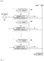
- FIG. 1 is an example of a lighting system including an LED lighting device.
- an LED lighting device 10 receives power from a power source 20 and includes an LED array 12 and a dimming circuit 14.
- a plurality of LED lighting devices 10 can be controlled by one dimmer 30.
- the dimming circuit having the isolation structure includes an isolation transformer which isolates a primary coil of an LED array and a secondary coil of a dimmer, and accordingly, the failure which occurs from the one LED lighting device may not be spread to other LED lighting devices.
- a dimming circuit having a general isolation structure uses a plurality of semiconductor elements, and thus has high circuit complexity, and it is difficult to accurately control dimming thereof. Further, since large inductance is demanded and thus the size of an isolation transformer increases, cost efficiency and space efficiency are low.
- the present invention is directed to providing a light emitting diode (LED) lighting device including an isolation transformer, and a dimming control method thereof.
- LED light emitting diode
- One aspect of the present invention provides a light emitting diode (LED) lighting device including an LED array; a first control unit configured to control dimming of the LED array; a second control unit configured to transmit a dimming control signal, which controls the dimming of the LED array, to the first control unit; and a transformer including a primary coil and a secondary coil spaced apart from each other, wherein the first control unit is connected to the primary coil and the second control unit is connected to the secondary coil, the primary coil and the secondary coil are isolated from each other, the transformer transmits a pulse signal, which is repeatedly turned on and turned off at a predetermined interval, from the first control unit to the second control unit, the dimming control signal is transmitted from the second control unit to the first control unit through the transformer when the pulse signal transmitted from the first control unit to the second control unit through the transformer is turned off, and the first control unit rectifies the dimming control signal which is an alternating current signal transmitted from the second control unit to the first control unit through the transformer to a direct current signal and then controls the
- the first control unit may include a rectifier, which includes a diode configured to rectify the dimming control signal and a capacitor connected between the diode and a direct current power source, and an offset voltage cancellation part configured to cancel the offset voltage from a signal output from the rectifier, and the offset voltage may include a voltage value of the direct current power source.
- a rectifier which includes a diode configured to rectify the dimming control signal and a capacitor connected between the diode and a direct current power source, and an offset voltage cancellation part configured to cancel the offset voltage from a signal output from the rectifier, and the offset voltage may include a voltage value of the direct current power source.
- the offset voltage cancellation part may cancel the offset voltage using voltage distribution.
- the offset voltage cancellation part may include a plurality of resistors connected in series between the rectifier and the LED array, and a Zener diode or shunt regulator connected to one of the plurality of resistors in parallel.
- the dimming control signal may be a signal in which a predetermined correction voltage is added to a voltage output from a dimmer.
- the correction voltage may be generated by the plurality of resistors connected in series to the dimmer and the Zener diode or shunt regulator connected to the one of the plurality of resistors in parallel.
- the offset voltage may further include the correction voltage.
- Another aspect of the present invention provides a dimming control method of a light emitting diode (LED) lighting device including: generating a pulse signal, which is repeatedly turned on and turned off at a predetermined interval, in a first control unit including an LED array; transmitting the pulse signal generated in the first control unit to a second control unit including a dimmer through a transformer; transmitting, by the second control unit, a dimming control signal which controls the LED array to the first control unit through the transformer when the pulse signal of the first control unit transmitted through the transformer is turned off; rectifying, by the first control unit, the dimming control signal, which is an alternating current signal transmitted through the transformer, to a direct current signal; cancelling, by the first control unit, an offset voltage from the rectified signal; and controlling, by the first control unit, dimming of the LED array using a signal from which the offset voltage is cancelled.
- LED light emitting diode
- a voltage of the signal from which the offset voltage is cancelled may be the same as a voltage output from the dimmer.
- a simple structure can be realized, and a dimming circuit having high accuracy and isolation can be obtained using a small number of switching elements. Accordingly, dimming of a light emitting diode (LED) lighting device is easy and production costs of the LED lighting device can be reduced. Further, according to the embodiment of the present invention, since accuracy of dimming is not largely influenced by an inductance value of a transformer, the inductance value can be designed to be low, and a transformer having a small size can be used.
- the elements may include not only a case of being directly connected, coupled, or linked to other elements but also a case of being connected, coupled, or linked to other elements by elements between the elements and other elements.
- the term “on or under” includes both a case in which the two elements are in direct contact with each other and a case in which at least another element is disposed between the two elements (indirectly). Further, when the term “on or under” is expressed, a meaning of not only an upward direction but also a downward direction may be included with respect to one element.
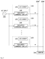
- FIG. 2 illustrates a lighting system including a light emitting diode (LED) lighting device according to one embodiment of the present invention.
- LED light emitting diode
- an LED lighting device 100 receives power from a power source 200 and includes an LED array 120 and a dimming circuit 140.
- a plurality of LED lighting devices 100 may be controlled by one dimmer 300.
- the dimming circuit 140 is an isolation dimming circuit including a transformer which isolates a primary coil in the LED array 120 and a secondary coil in the dimmer 300. Accordingly, even when a failure occurs due to an overvoltage such as a short circuit or surge to one of the plurality of LED lighting devices 100, a problem that the failure is spread to the dimmer 300 or is spread to another LED lighting device 10 adjacent to the one LED lighting device may be prevented.
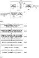
- FIG. 3 is a block diagram of the lighting system in the LED lighting device according to one embodiment of the present invention
- FIG. 4 is a flow chart illustrating a dimming control method of the lighting system in the LED lighting device according to one embodiment of the present invention.
- the dimming circuit 140 includes a first control unit 142, a second control unit 144, and a transformer 146.
- the first control unit 142 is connected to the LED array 120 and controls dimming of the LED array 120.
- the second control unit 144 is connected to the dimmer 300 and receives a dimming control signal for controlling the LED array 120 from the dimmer 300 and then transmits the dimming control signal to the first control unit 142.
- the transformer 146 includes a primary coil T1 and a secondary coil T2 spaced apart from each other, and the primary coil T1 may be connected to the first control unit 142 and the secondary coil T2 may be connected to the second control unit 144.
- the primary coil T1 and the secondary coil T2 may be isolated. Accordingly, in the specification, the transformer 146 may be used together with the isolation transformer 146. Further, the transformer 146 may have a turn ratio of 1 to 1 between the primary coil T1 and the secondary coil T2 and operate in a flyback manner.
- the first control unit 142 may include a pulse generator 1422, a signal rectifier 1424, and an offset voltage cancellation part 1426, and the second control unit 144 may be used together with a signal processor.
- the pulse generator 1422 of the first control unit 142 generates a pulse signal, which is repeatedly turned on and turned off at a predetermined interval (S400), and transmits the generated pulse signal to the second control unit 144 through the transformer 146 (S410).
- the pulse signal may be a pulse width modulation (PWM) signal and may be a signal having a predetermined duty ratio with respect to a voltage value of direct current power input to the first control unit 142, for example, a duty ratio of 30%.
- PWM pulse width modulation
- the second control unit 144 transmits the dimming control signal for controlling the LED array 120 to the first control unit 142 through the transformer 146 (S420).
- the dimming control signal may have a value output from the dimmer 300 to control brightness of the LED array 120 and have a value set by a user or a value automatically set according to ambient light.
- the dimming control signal may have a value of 0 to 10 V, or 1 to 10 V, and accordingly, the LED array 120 becomes brighter when the value increases, and the LED array 120 becomes darker when the value decreases.
- the dimming control signal may be a signal in which a predetermined correction voltage is added to the voltage output from the dimmer 300.
- the predetermined correction voltage may be a value added so that the dimming control signal is processed to be readable in the first control unit 142 or so that the voltage output from the dimmer 300 maintains a stable value.
- the dimming control signal transmitted from the second control unit 144 to the first control unit 142 through the transformer 146 may be an alternating current signal. Accordingly, the first control unit 142 rectifies the dimming control signal which is the alternating current signal to a direct current signal (S430). To this end, the signal rectifier 1424 may include a diode and a capacitor, and the dimming control signal transmitted from the second control unit 144 may be rectified to the direct current signal through the diode and then stored in the capacitor.
- one end of the capacitor may be connected to the direct current power source, and accordingly, a value output from the signal rectifier 1424 may be a value in which a voltage value of the direct current power is added to the dimming control signal transmitted from the second control unit 144.
- the offset voltage cancellation part 1426 of the first control unit 142 cancels an offset voltage from a signal rectified by the signal rectifier 1424 of the first control unit 142 (S440) and then controls the dimming of the LED array 120 (S450).
- the offset voltage may refer to a value added to the voltage output from the dimmer 300 to control the dimming of the LED array 120.
- the offset voltage may include the voltage value of the direct current power added in the signal rectifier 1424.
- the offset voltage may further include the correction voltage added to the voltage output from the dimmer 300 in the second control unit 144. Accordingly, a voltage of the signal from which the offset voltage is cancelled may be the same as the voltage output from the dimmer 300.
- a main control unit may be further disposed between the offset voltage cancellation part 1426 and the LED array 120.
- the dimming control signal may be converted to a value which is the same as a value of the voltage output from the dimmer 300, that is, a value readable by the MCU.
- FIG. 5 illustrates a circuit diagram of a dimming circuit in the LED lighting device according to one embodiment of the present invention.
- the dimming circuit 140 includes the first control unit 142, the second control unit 144, and the transformer 146.
- the first control unit 142 is connected to the LED array 120 and controls the dimming of the LED array 120.
- the second control unit 144 is connected to the dimmer 300 and receives the dimming control signal for controlling the LED array 120 from the dimmer 300 and then transmits the dimming control signal to the first control unit 142.
- the first control unit 142 and the LED array 120 are separate configurations and the first control unit 142 is connected to the LED array 120, but the present invention is not limited thereto.
- the first control unit 142 may be included in the LED array 120 or the LED array may be included in the first control unit 142.
- the second control unit 144 and the dimmer 300 are separate configurations and the second control unit 144 is connected to the dimmer 300, but the present invention is not limited thereto.
- the second control unit 144 may be included in the dimmer 300 or the dimmer 300 may be included in the second control unit 144.
- the transformer 146 includes the primary coil T1 connected to the first control unit 142 and the secondary coil T2 connected to the second control unit 144, and the primary coil T1 and the secondary coil T2 are isolated.
- the transformer 146 may have a turn ratio of 1 to 1 between the primary coil T1 and the secondary coil T2 and operate in the flyback manner.
- the first control unit 142 may include the pulse generator 1422, the signal rectifier 1424, and the offset voltage cancellation part 1426, and the second control unit 144 may be used together with the signal processor.
- the pulse generator 1422 of the first control unit 142 generates a pulse signal which is repeatedly turned on and turned off at a predetermined interval.
- the pulse generator 1422 includes a transistor Q1, for example, a field effect transistor (FET), and the pulse signal may be applied to a gate electrode of the transistor Q1. Further, a drain electrode of the transistor Q1 may be connected to the primary coil T1 of the transformer 146.
- FET field effect transistor
- the pulse signal generated from the pulse generator 1422 is transmitted to the second control unit 144 through the transformer 146.
- the pulse signal may have a predetermined duty ratio with respect to a Volts Direct Current (VDC) which is a voltage value of the direct current power input to the first control unit 142.
- VDC Volts Direct Current
- a pulse signal of which the duty ratio of 12 V is 30% is ordinarily applied to a P1 node of the second control unit 144.
- the second control unit 144 receives the dimming control signal from the dimmer 300 through a DIM+ line and a DIM- line.
- the dimming control signal has a value output from the dimmer 300 to control the brightness of the LED array 120, and may have a value set by the user or a value automatically set according to the ambient light.
- the dimming control signal may have a value of 0 to 10 V or 1 to 10 V, and accordingly, the LED array 120 becomes brighter when the value increases, and the LED array 120 becomes darker when the value decreases.
- a Zener diode ZD1 may be connected between the DIM+ line and the DIM- line
- the second control unit 144 may add a predetermined correction voltage to the voltage output from the dimmer 300.
- the predetermined correction voltage may be a value added so that the dimming control signal is processed to be readable in the first control unit 142, or the voltage output from the dimmer 300 maintains a stable value.
- the correction voltage may be added by voltage distribution.
- the second control unit 144 may include two resistors R5 and R6 connected in series to the DIM-, a shunt regulator U2 or Zener diode connected to the resistor R5 in parallel, and a capacitor C4 connected to the resistor R5 in parallel.
- a level of the correction voltage may be controlled according to a resistance ratio between the two resistors R5 and R6, and a stable value may be maintained according to the shunt regulator or Zener diode.
- the pulse signal transmitted from the first control unit 142 is ordinarily applied to the P1 node, when the voltage value for controlling the dimming of the LED array 120 is output from the dimmer 300, the dimming control signal is applied to the P1 node. Further, when the pulse signal transmitted from the first control unit 142 is turned off, the value applied to the P1 node is applied to the first control unit 142 through the transformer 146 using the flyback manner. Accordingly, the dimming control signal transmitted from the second control unit 144 may be reflected to a P3 node of the first control unit 142.
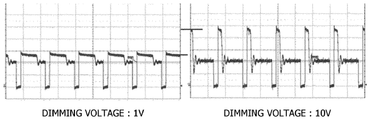
- FIG. 6 illustrates an example of dimming control information transmitted to the P3 node. In FIG. 6 , an example in which the value of the voltage output from the dimmer 300 has a value of 1 V and a value of 10 V is described.
- the dimming control signal reflected to the P3 node is rectified by the signal rectifier 1424 of the first control unit 142.
- the signal rectifier 1424 may include a diode D1 and a capacitor C1.
- One end of the diode may be connected to the P3 node, and the other end may be connected to the P2 node.
- one end of the capacitor C1 may be connected to VDC which is the direct current power, and the other end of the capacitor C1 may be connected to the P2 node.
- the dimming control signal which is an alternating current signal reflected to the P3 node is rectified to the direct current signal through the diodeD1 and then stored in the capacitor C1.
- the signal rectifier 1424 may include some components of a snubber circuit.
- the snubber circuit is a circuit which serves to cut spikes due to a cap component of the pulse signal and may be used to detect a level of the dimming control signal.
- the offset voltage cancellation part 1426 of the first control unit 142 cancels the offset voltage from a voltage applied to the P2 node and then controls the dimming of the LED array 120.
- the offset voltage may be a value added to the value of the voltage output from the dimmer 300.
- the offset voltage may include the voltage value of the direct current power added in the signal rectifier 1424.
- the offset voltage may further include a predetermined correction voltage added in the second control unit 144.
- the offset voltage cancellation part 1426 may cancel the offset voltage using the voltage distribution.
- the offset voltage cancellation part 1426 may include two resistors R1 and R2 which are connected in series, a shunt regulator U1, and a capacitor 2, one end of the resistor R1 may be connected to the P2 node, the other end of the resistor R1 may be connected to the other resistor R2, and the capacitor 2 and the shunt regulator U1 may be connected to the resistor R2 in parallel. Accordingly, the offset voltage may be cancelled from the voltage applied to the P2 node, and a value actually output from the dimmer 300 may be applied for the dimming of the LED array 120.
- the dimming circuit since the dimming circuit includes the isolation transformer, although a failure occurs in one LED lighting device in the lighting system including the plurality of LED lighting devices, the failure may not be spread to other LED lighting device or the dimmer.
- the pulse signal of the first control unit is transmitted to the second control unit, and the dimming control signal of the second control unit is transmitted to the first control unit in the flyback manner, and then a rectifying process and an offset voltage cancelling process are performed, and thus accurate dimming control may be performed using a simple circuit structure.
- LED lighting device 120 LED array 140: dimming circuit 142: first control unit 144: second control unit 146: isolation transformer 300: dimmer 1422: pulse generator 1424: signal rectifier 1426: offset voltage cancellation part
Landscapes
- Engineering & Computer Science (AREA)
- Power Engineering (AREA)
- Circuit Arrangement For Electric Light Sources In General (AREA)
Abstract
Description
- The present invention relates to a light emitting diode (LED) lighting device, and more specifically, to a dimming control method of an LED lighting device.
- A fluorescent lamp, an incandescent lamp, a light emitting diode (LED), and the like are used as indoor and outdoor lighting devices. Among the above, the lighting device using the LED has low power consumption and is semi-permanent in comparison with the fluorescent lamp.
-
FIG. 1 is an example of a lighting system including an LED lighting device. - Referring to
FIG. 1 , anLED lighting device 10 receives power from apower source 20 and includes anLED array 12 and adimming circuit 14. - A plurality of
LED lighting devices 10 can be controlled by onedimmer 30. - In this case, when a failure occurs due to an overvoltage such as a short circuit or surge to one of the plurality of
LED lighting devices 10, the failure is spread to thedimmer 30 through DIM+ and DIM- wires. Accordingly, since the failure is spread to otherLED lighting devices 10 which stably operate, secondary damage can occur. - Accordingly, there is an attempt to use a dimming circuit having an isolation structure. The dimming circuit having the isolation structure includes an isolation transformer which isolates a primary coil of an LED array and a secondary coil of a dimmer, and accordingly, the failure which occurs from the one LED lighting device may not be spread to other LED lighting devices.
- Meanwhile, a dimming circuit having a general isolation structure uses a plurality of semiconductor elements, and thus has high circuit complexity, and it is difficult to accurately control dimming thereof. Further, since large inductance is demanded and thus the size of an isolation transformer increases, cost efficiency and space efficiency are low.
- The present invention is directed to providing a light emitting diode (LED) lighting device including an isolation transformer, and a dimming control method thereof.
- One aspect of the present invention provides a light emitting diode (LED) lighting device including an LED array; a first control unit configured to control dimming of the LED array; a second control unit configured to transmit a dimming control signal, which controls the dimming of the LED array, to the first control unit; and a transformer including a primary coil and a secondary coil spaced apart from each other, wherein the first control unit is connected to the primary coil and the second control unit is connected to the secondary coil, the primary coil and the secondary coil are isolated from each other, the transformer transmits a pulse signal, which is repeatedly turned on and turned off at a predetermined interval, from the first control unit to the second control unit, the dimming control signal is transmitted from the second control unit to the first control unit through the transformer when the pulse signal transmitted from the first control unit to the second control unit through the transformer is turned off, and the first control unit rectifies the dimming control signal which is an alternating current signal transmitted from the second control unit to the first control unit through the transformer to a direct current signal and then controls the dimming of the LED array using a value in which an offset voltage is cancelled.
- The first control unit may include a rectifier, which includes a diode configured to rectify the dimming control signal and a capacitor connected between the diode and a direct current power source, and an offset voltage cancellation part configured to cancel the offset voltage from a signal output from the rectifier, and the offset voltage may include a voltage value of the direct current power source.
- The offset voltage cancellation part may cancel the offset voltage using voltage distribution.
- The offset voltage cancellation part may include a plurality of resistors connected in series between the rectifier and the LED array, and a Zener diode or shunt regulator connected to one of the plurality of resistors in parallel.
- The dimming control signal may be a signal in which a predetermined correction voltage is added to a voltage output from a dimmer.
- The correction voltage may be generated by the plurality of resistors connected in series to the dimmer and the Zener diode or shunt regulator connected to the one of the plurality of resistors in parallel.
- The offset voltage may further include the correction voltage.
- Another aspect of the present invention provides a dimming control method of a light emitting diode (LED) lighting device including: generating a pulse signal, which is repeatedly turned on and turned off at a predetermined interval, in a first control unit including an LED array; transmitting the pulse signal generated in the first control unit to a second control unit including a dimmer through a transformer; transmitting, by the second control unit, a dimming control signal which controls the LED array to the first control unit through the transformer when the pulse signal of the first control unit transmitted through the transformer is turned off; rectifying, by the first control unit, the dimming control signal, which is an alternating current signal transmitted through the transformer, to a direct current signal; cancelling, by the first control unit, an offset voltage from the rectified signal; and controlling, by the first control unit, dimming of the LED array using a signal from which the offset voltage is cancelled.
- A voltage of the signal from which the offset voltage is cancelled may be the same as a voltage output from the dimmer.
- According to an embodiment of the present invention, a simple structure can be realized, and a dimming circuit having high accuracy and isolation can be obtained using a small number of switching elements. Accordingly, dimming of a light emitting diode (LED) lighting device is easy and production costs of the LED lighting device can be reduced. Further, according to the embodiment of the present invention, since accuracy of dimming is not largely influenced by an inductance value of a transformer, the inductance value can be designed to be low, and a transformer having a small size can be used.
-
-
FIG. 1 is an example of a lighting system including a light emitting diode (LED) lighting device. -
FIG. 2 illustrates a lighting system including an LED lighting device according to one embodiment of the present invention. -
FIG. 3 is a block diagram of the lighting system in the LED lighting device according to one embodiment of the present invention. -
FIG. 4 is a flow chart illustrating a dimming control method of the LED lighting device according to one embodiment of the present invention. -
FIG. 5 illustrates a circuit diagram of a dimming circuit in the LED lighting device according to one embodiment of the present invention. -
FIG. 6 illustrates an example of dimming control information transmitted to a P3 node. - Hereinafter, preferable embodiments of the present invention will be described in detail with reference to the accompanying drawings.
- However, the technical spirit of the present invention is not limited to some embodiments which will be described and may be embodied in various forms, and one or more elements in the embodiments may be selectively combined and replaced to be used within the scope of the technical spirit of the present invention.
- Further, terms used in the embodiments of the present invention (including technical and scientific terms), may be interpreted with meanings that are generally understood by those skilled in the art unless particularly defined and described, and terms which are generally used, such as terms defined in a dictionary, may be understood in consideration of their contextual meanings in the related art.
- In addition, terms used in the description are provided not to limit the present invention but to describe the embodiments.
- In the specification, the singular form may also include the plural form unless the context clearly indicates otherwise and may include one or more of all possible combinations of A, B, and C when disclosed as at least one (or one or more) of "A, B, and C".
- In addition, terms such as first, second, A, B, (a), (b), and the like may be used to describe elements of the embodiments of the present invention.
- The terms are only provided to distinguish the elements from other elements, and the essence, sequence, order, or the like of the elements are not limited by the terms.
- Further, when particular elements are disclosed as being "connected," "coupled," or "linked" to other elements, the elements may include not only a case of being directly connected, coupled, or linked to other elements but also a case of being connected, coupled, or linked to other elements by elements between the elements and other elements.
- In addition, when one element is disclosed as being formed "on or under" another element, the term "on or under" includes both a case in which the two elements are in direct contact with each other and a case in which at least another element is disposed between the two elements (indirectly). Further, when the term "on or under" is expressed, a meaning of not only an upward direction but also a downward direction may be included with respect to one element.
-
FIG. 2 illustrates a lighting system including a light emitting diode (LED) lighting device according to one embodiment of the present invention. - Referring to
FIG. 2 , anLED lighting device 100 receives power from apower source 200 and includes anLED array 120 and adimming circuit 140. - A plurality of
LED lighting devices 100 may be controlled by onedimmer 300. - In this case, the
dimming circuit 140 is an isolation dimming circuit including a transformer which isolates a primary coil in theLED array 120 and a secondary coil in thedimmer 300. Accordingly, even when a failure occurs due to an overvoltage such as a short circuit or surge to one of the plurality ofLED lighting devices 100, a problem that the failure is spread to thedimmer 300 or is spread to anotherLED lighting device 10 adjacent to the one LED lighting device may be prevented. -
FIG. 3 is a block diagram of the lighting system in the LED lighting device according to one embodiment of the present invention, andFIG. 4 is a flow chart illustrating a dimming control method of the lighting system in the LED lighting device according to one embodiment of the present invention. - Referring to
FIG. 3 , thedimming circuit 140 includes afirst control unit 142, asecond control unit 144, and atransformer 146. - The
first control unit 142 is connected to theLED array 120 and controls dimming of theLED array 120. Thesecond control unit 144 is connected to thedimmer 300 and receives a dimming control signal for controlling theLED array 120 from thedimmer 300 and then transmits the dimming control signal to thefirst control unit 142. Further, thetransformer 146 includes a primary coil T1 and a secondary coil T2 spaced apart from each other, and the primary coil T1 may be connected to thefirst control unit 142 and the secondary coil T2 may be connected to thesecond control unit 144. In addition, in thetransformer 146 according to the embodiment of the present invention, the primary coil T1 and the secondary coil T2 may be isolated. Accordingly, in the specification, thetransformer 146 may be used together with theisolation transformer 146. Further, thetransformer 146 may have a turn ratio of 1 to 1 between the primary coil T1 and the secondary coil T2 and operate in a flyback manner. - More specifically, referring to
FIGS. 3 and 4 , thefirst control unit 142 may include apulse generator 1422, asignal rectifier 1424, and an offsetvoltage cancellation part 1426, and thesecond control unit 144 may be used together with a signal processor. - The
pulse generator 1422 of thefirst control unit 142 generates a pulse signal, which is repeatedly turned on and turned off at a predetermined interval (S400), and transmits the generated pulse signal to thesecond control unit 144 through the transformer 146 (S410). In this case, the pulse signal may be a pulse width modulation (PWM) signal and may be a signal having a predetermined duty ratio with respect to a voltage value of direct current power input to thefirst control unit 142, for example, a duty ratio of 30%. - When the pulse signal transmitted from the
first control unit 142 to thesecond control unit 144 through thetransformer 146 is turned off, thesecond control unit 144 transmits the dimming control signal for controlling theLED array 120 to thefirst control unit 142 through the transformer 146 (S420). Here, the dimming control signal may have a value output from the dimmer 300 to control brightness of theLED array 120 and have a value set by a user or a value automatically set according to ambient light. For example, the dimming control signal may have a value of 0 to 10 V, or 1 to 10 V, and accordingly, theLED array 120 becomes brighter when the value increases, and theLED array 120 becomes darker when the value decreases. Alternatively, the dimming control signal may be a signal in which a predetermined correction voltage is added to the voltage output from the dimmer 300. The predetermined correction voltage may be a value added so that the dimming control signal is processed to be readable in thefirst control unit 142 or so that the voltage output from the dimmer 300 maintains a stable value. - The dimming control signal transmitted from the
second control unit 144 to thefirst control unit 142 through thetransformer 146 may be an alternating current signal. Accordingly, thefirst control unit 142 rectifies the dimming control signal which is the alternating current signal to a direct current signal (S430). To this end, thesignal rectifier 1424 may include a diode and a capacitor, and the dimming control signal transmitted from thesecond control unit 144 may be rectified to the direct current signal through the diode and then stored in the capacitor. In this case, one end of the capacitor may be connected to the direct current power source, and accordingly, a value output from thesignal rectifier 1424 may be a value in which a voltage value of the direct current power is added to the dimming control signal transmitted from thesecond control unit 144. - Further, the offset
voltage cancellation part 1426 of thefirst control unit 142 cancels an offset voltage from a signal rectified by thesignal rectifier 1424 of the first control unit 142 (S440) and then controls the dimming of the LED array 120 (S450). The offset voltage may refer to a value added to the voltage output from the dimmer 300 to control the dimming of theLED array 120. For example, the offset voltage may include the voltage value of the direct current power added in thesignal rectifier 1424. Alternatively, the offset voltage may further include the correction voltage added to the voltage output from the dimmer 300 in thesecond control unit 144. Accordingly, a voltage of the signal from which the offset voltage is cancelled may be the same as the voltage output from the dimmer 300. - Although not shown, a main control unit (MCU) may be further disposed between the offset
voltage cancellation part 1426 and theLED array 120. When the offset voltage is cancelled, the dimming control signal may be converted to a value which is the same as a value of the voltage output from the dimmer 300, that is, a value readable by the MCU. - Hereinafter, it will be described more specifically with reference to a circuit diagram.
-
FIG. 5 illustrates a circuit diagram of a dimming circuit in the LED lighting device according to one embodiment of the present invention. - Referring to
FIG. 5 , thedimming circuit 140 includes thefirst control unit 142, thesecond control unit 144, and thetransformer 146. - The
first control unit 142 is connected to theLED array 120 and controls the dimming of theLED array 120. Thesecond control unit 144 is connected to the dimmer 300 and receives the dimming control signal for controlling theLED array 120 from the dimmer 300 and then transmits the dimming control signal to thefirst control unit 142. Here, it is shown and described that thefirst control unit 142 and theLED array 120 are separate configurations and thefirst control unit 142 is connected to theLED array 120, but the present invention is not limited thereto. Thefirst control unit 142 may be included in theLED array 120 or the LED array may be included in thefirst control unit 142. As described above, it is shown and described that thesecond control unit 144 and the dimmer 300 are separate configurations and thesecond control unit 144 is connected to the dimmer 300, but the present invention is not limited thereto. Thesecond control unit 144 may be included in the dimmer 300 or the dimmer 300 may be included in thesecond control unit 144. Further, thetransformer 146 includes the primary coil T1 connected to thefirst control unit 142 and the secondary coil T2 connected to thesecond control unit 144, and the primary coil T1 and the secondary coil T2 are isolated. Here, thetransformer 146 may have a turn ratio of 1 to 1 between the primary coil T1 and the secondary coil T2 and operate in the flyback manner. - More specifically, the
first control unit 142 may include thepulse generator 1422, thesignal rectifier 1424, and the offsetvoltage cancellation part 1426, and thesecond control unit 144 may be used together with the signal processor. - The
pulse generator 1422 of thefirst control unit 142 generates a pulse signal which is repeatedly turned on and turned off at a predetermined interval. Thepulse generator 1422 includes a transistor Q1, for example, a field effect transistor (FET), and the pulse signal may be applied to a gate electrode of the transistor Q1. Further, a drain electrode of the transistor Q1 may be connected to the primary coil T1 of thetransformer 146. - Accordingly, the pulse signal generated from the
pulse generator 1422 is transmitted to thesecond control unit 144 through thetransformer 146. In this case, the pulse signal may have a predetermined duty ratio with respect to a Volts Direct Current (VDC) which is a voltage value of the direct current power input to thefirst control unit 142. For example, when VDC is 12 V and the duty ratio is 30%, a pulse signal of which the duty ratio of 12 V is 30% is ordinarily applied to a P1 node of thesecond control unit 144. - Meanwhile, when the dimmer 300 outputs a voltage value for controlling the dimming of the
LED array 120, thesecond control unit 144, that is, a signal processor, receives the dimming control signal from the dimmer 300 through a DIM+ line and a DIM- line. Here, the dimming control signal has a value output from the dimmer 300 to control the brightness of theLED array 120, and may have a value set by the user or a value automatically set according to the ambient light. For example, the dimming control signal may have a value of 0 to 10 V or 1 to 10 V, and accordingly, theLED array 120 becomes brighter when the value increases, and theLED array 120 becomes darker when the value decreases. In order to obtain a constant voltage, a Zener diode ZD1 may be connected between the DIM+ line and the DIM- line - In this case, the
second control unit 144 may add a predetermined correction voltage to the voltage output from the dimmer 300. The predetermined correction voltage may be a value added so that the dimming control signal is processed to be readable in thefirst control unit 142, or the voltage output from the dimmer 300 maintains a stable value. The correction voltage may be added by voltage distribution. To this end, thesecond control unit 144 may include two resistors R5 and R6 connected in series to the DIM-, a shunt regulator U2 or Zener diode connected to the resistor R5 in parallel, and a capacitor C4 connected to the resistor R5 in parallel. A level of the correction voltage may be controlled according to a resistance ratio between the two resistors R5 and R6, and a stable value may be maintained according to the shunt regulator or Zener diode. - Although the pulse signal transmitted from the
first control unit 142 is ordinarily applied to the P1 node, when the voltage value for controlling the dimming of theLED array 120 is output from the dimmer 300, the dimming control signal is applied to the P1 node. Further, when the pulse signal transmitted from thefirst control unit 142 is turned off, the value applied to the P1 node is applied to thefirst control unit 142 through thetransformer 146 using the flyback manner. Accordingly, the dimming control signal transmitted from thesecond control unit 144 may be reflected to a P3 node of thefirst control unit 142.FIG. 6 illustrates an example of dimming control information transmitted to the P3 node. InFIG. 6 , an example in which the value of the voltage output from the dimmer 300 has a value of 1 V and a value of 10 V is described. - Further, the dimming control signal reflected to the P3 node is rectified by the
signal rectifier 1424 of thefirst control unit 142. To this end, thesignal rectifier 1424 may include a diode D1 and a capacitor C1. One end of the diode may be connected to the P3 node, and the other end may be connected to the P2 node. Further, one end of the capacitor C1 may be connected to VDC which is the direct current power, and the other end of the capacitor C1 may be connected to the P2 node. Accordingly, the dimming control signal which is an alternating current signal reflected to the P3 node is rectified to the direct current signal through the diodeD1 and then stored in the capacitor C1. Accordingly, a value in which the voltage value of the direct current power (VDC) is added to the dimming control signal reflected to the P3 node may be applied to the P2 node. To this end, thesignal rectifier 1424 may include some components of a snubber circuit. The snubber circuit is a circuit which serves to cut spikes due to a cap component of the pulse signal and may be used to detect a level of the dimming control signal. - Further, the offset
voltage cancellation part 1426 of thefirst control unit 142 cancels the offset voltage from a voltage applied to the P2 node and then controls the dimming of theLED array 120. The offset voltage may be a value added to the value of the voltage output from the dimmer 300. For example, the offset voltage may include the voltage value of the direct current power added in thesignal rectifier 1424. The offset voltage may further include a predetermined correction voltage added in thesecond control unit 144. - The offset
voltage cancellation part 1426 may cancel the offset voltage using the voltage distribution. To this end, the offsetvoltage cancellation part 1426 may include two resistors R1 and R2 which are connected in series, a shunt regulator U1, and a capacitor 2, one end of the resistor R1 may be connected to the P2 node, the other end of the resistor R1 may be connected to the other resistor R2, and the capacitor 2 and the shunt regulator U1 may be connected to the resistor R2 in parallel. Accordingly, the offset voltage may be cancelled from the voltage applied to the P2 node, and a value actually output from the dimmer 300 may be applied for the dimming of theLED array 120. - According to the embodiment of the present invention, since the dimming circuit includes the isolation transformer, although a failure occurs in one LED lighting device in the lighting system including the plurality of LED lighting devices, the failure may not be spread to other LED lighting device or the dimmer.
- Further, according to the embodiment of the present invention, the pulse signal of the first control unit is transmitted to the second control unit, and the dimming control signal of the second control unit is transmitted to the first control unit in the flyback manner, and then a rectifying process and an offset voltage cancelling process are performed, and thus accurate dimming control may be performed using a simple circuit structure.
- Although preferable embodiments of the present invention are described above, those skilled in the art may variously modify and change the present invention within the scope of the spirit and the area of the present invention disclosed in the claims which will be described later.
[Reference numerals] 100: LED lighting device 120: LED array 140: dimming circuit 142: first control unit 144: second control unit 146: isolation transformer 300: dimmer 1422: pulse generator 1424: signal rectifier 1426: offset voltage cancellation part
Claims (10)
- A light emitting diode (LED) lighting device comprising:an LED array;a first control unit configured to control dimming of the LED array;a second control unit configured to transmit a dimming control signal, which controls the dimming of the LED array, to the first control unit; anda transformer including a primary coil and a secondary coil spaced apart from each other,wherein the first control unit is connected to the primary coil and the second control unit is connected to the secondary coil,the primary coil and the secondary coil are isolated from each other,the transformer transmits a pulse signal, which is repeatedly turned on and turned off at a predetermined interval, from the first control unit to the second control unit,the dimming control signal is transmitted from the second control unit to the first control unit through the transformer when the pulse signal transmitted from the first control unit to the second control unit through the transformer is turned off, andthe first control unit rectifies the dimming control signal which is an alternating current signal transmitted from the second control unit to the first control unit through the transformer to a direct current signal and then controls the dimming of the LED array using a value in which an offset voltage is cancelled.
- The LED lighting device of claim 1, wherein:the first control unit includes a rectifier, which includes a diode configured to rectify the dimming control signal and a capacitor connected between the diode and a direct current power source, and an offset voltage cancellation part configured to cancel the offset voltage from a signal output from the rectifier; andthe offset voltage includes a voltage value of the direct current power source.
- The LED lighting device of claim 2, wherein the offset voltage cancellation part cancels the offset voltage using voltage distribution.
- The LED lighting device of claim 3, wherein the offset voltage cancellation part includes a plurality of resistors connected in series between the rectifier and the LED array, and a Zener diode or shunt regulator connected to one of the plurality of resistors in parallel.
- The LED lighting device of claim 2, wherein the dimming control signal is a signal in which a predetermined correction voltage is added to a voltage output from a dimmer.
- The LED lighting device of claim 4, wherein a correction voltage is generated by the plurality of resistors connected in series to a dimmer and the Zener diode or shunt regulator connected to one of the plurality of resistors in parallel.
- The LED lighting device of claim 6, wherein the offset voltage further includes the correction voltage.
- A dimming control method of a light emitting diode (LED) lighting device, comprising:generating a pulse signal, which is repeatedly turned on and turned off at a predetermined interval, in a first control unit including an LED array;transmitting the pulse signal generated in the first control unit to a second control unit including a dimmer through a transformer;transmitting, by the second control unit, a dimming control signal which controls the LED array to the first control unit through the transformer when the pulse signal of the first control unit transmitted through the transformer is turned off;rectifying, by the first control unit, the dimming control signal, which is an alternating current signal transmitted through the transformer, to a direct current signal;cancelling, by the first control unit, an offset voltage from the rectified signal; andcontrolling, by the first control unit, dimming of the LED array using a signal from which the offset voltage is cancelled.
- The dimming control method of claim 8, wherein a voltage of the signal from which the offset voltage is cancelled is the same as a voltage output from the dimmer.
- The dimming control method of claim 8, wherein:the dimming control signal is rectified using a diode and then a voltage of a direct current power source is added in the rectifying operation; andthe voltage of the direct current power source is cancelled in the operation of cancelling the offset voltage.
Applications Claiming Priority (2)
| Application Number | Priority Date | Filing Date | Title |
|---|---|---|---|
| KR1020170092798A KR102385357B1 (en) | 2017-07-21 | 2017-07-21 | Led lighting device, and light control method of the same |
| PCT/KR2018/007919 WO2019017649A1 (en) | 2017-07-21 | 2018-07-12 | Led lighting device and dimming control method therefor |
Publications (3)
| Publication Number | Publication Date |
|---|---|
| EP3657910A1 true EP3657910A1 (en) | 2020-05-27 |
| EP3657910A4 EP3657910A4 (en) | 2021-04-07 |
| EP3657910B1 EP3657910B1 (en) | 2022-11-09 |
Family
ID=65016065
Family Applications (1)
| Application Number | Title | Priority Date | Filing Date |
|---|---|---|---|
| EP18835419.5A Active EP3657910B1 (en) | 2017-07-21 | 2018-07-12 | Led lighting device and dimming control method therefor |
Country Status (4)
| Country | Link |
|---|---|
| US (1) | US10834794B2 (en) |
| EP (1) | EP3657910B1 (en) |
| KR (1) | KR102385357B1 (en) |
| WO (1) | WO2019017649A1 (en) |
Families Citing this family (3)
| Publication number | Priority date | Publication date | Assignee | Title |
|---|---|---|---|---|
| CN110213856A (en) * | 2019-06-06 | 2019-09-06 | 矽力杰半导体技术(杭州)有限公司 | Light adjusting circuit and method |
| KR102765517B1 (en) * | 2021-04-19 | 2025-02-12 | 삼성전자주식회사 | Electronic apparatus and control method thereof |
| US11910499B2 (en) | 2021-04-19 | 2024-02-20 | Samsung Electronics Co., Ltd. | Electronic apparatus and control method thereof |
Family Cites Families (12)
| Publication number | Priority date | Publication date | Assignee | Title |
|---|---|---|---|---|
| US7855520B2 (en) * | 2008-03-19 | 2010-12-21 | Niko Semiconductor Co., Ltd. | Light-emitting diode driving circuit and secondary side controller for controlling the same |
| KR100946093B1 (en) * | 2008-05-29 | 2010-03-10 | 삼성전기주식회사 | Power supply for LED |
| KR100966339B1 (en) * | 2008-06-11 | 2010-06-28 | 삼성전기주식회사 | Lighting drive |
| CN102238768B (en) * | 2010-04-26 | 2014-04-09 | 光宝电子(广州)有限公司 | Light emitting diode backlight source driving module |
| KR20110132188A (en) * | 2010-05-31 | 2011-12-07 | 주식회사 파워넷 | LED driving device with improved power factor |
| JP5043213B2 (en) * | 2010-08-23 | 2012-10-10 | シャープ株式会社 | LED drive circuit and LED illumination lamp using the same |
| US20140092596A1 (en) * | 2012-09-28 | 2014-04-03 | Linear Lighting Corp. | Dimmable, high-efficiency led linear lighting system with interchangeable features and methods for producing same |
| US8836236B1 (en) * | 2013-05-03 | 2014-09-16 | Lee Chiang | LED offset voltage dimmer |
| KR20150059019A (en) * | 2013-11-21 | 2015-05-29 | 삼성전기주식회사 | Driving apparatus for light emitting diode |
| US9699868B2 (en) * | 2015-03-31 | 2017-07-04 | Infineon Technologies Austria Ag | Single isolation element for multiple interface standards |
| CN109644534B (en) * | 2016-08-29 | 2022-01-28 | 昕诺飞控股有限公司 | Control of isolated auxiliary and DALI power supplies for sensor-ready LED drivers |
| WO2018077695A1 (en) * | 2016-10-28 | 2018-05-03 | Philips Lighting Holding B.V. | A communication interface and arrangement |
-
2017
- 2017-07-21 KR KR1020170092798A patent/KR102385357B1/en active Active
-
2018
- 2018-07-12 EP EP18835419.5A patent/EP3657910B1/en active Active
- 2018-07-12 WO PCT/KR2018/007919 patent/WO2019017649A1/en not_active Ceased
- 2018-07-12 US US16/630,678 patent/US10834794B2/en active Active
Also Published As
| Publication number | Publication date |
|---|---|
| KR20190010261A (en) | 2019-01-30 |
| EP3657910A4 (en) | 2021-04-07 |
| US20200146125A1 (en) | 2020-05-07 |
| KR102385357B1 (en) | 2022-04-11 |
| US10834794B2 (en) | 2020-11-10 |
| EP3657910B1 (en) | 2022-11-09 |
| WO2019017649A1 (en) | 2019-01-24 |
Similar Documents
| Publication | Publication Date | Title |
|---|---|---|
| US9693402B2 (en) | Modular LED-lighting system | |
| US8760082B2 (en) | LED emitting device | |
| US20120319610A1 (en) | Led lighting apparatus | |
| KR20120112048A (en) | Led driving apparatus and led lighting apparatus | |
| US10880968B1 (en) | Independent, multiple channel LED driver for control of correlated color temperature | |
| JP6403042B2 (en) | Power supply apparatus and lighting apparatus using the same | |
| KR20180062965A (en) | Controller for multi-output single magnetic component converter with independent regulation of constant current and constant voltage outputs | |
| US20190098717A1 (en) | Ballast system, luminaire, lighting control system, lighting control method and non-transitory computer readable medium | |
| US10548189B2 (en) | Control of isolated auxiliary power supply and DALI supply for sensor-ready LED drivers | |
| JP2004273267A (en) | LED lighting device | |
| US20160105939A1 (en) | Dimmable led lighting apparatus | |
| US10051704B2 (en) | LED dimmer circuit and method | |
| US9320100B2 (en) | Lighting apparatus | |
| US10834794B2 (en) | LED lighting device and dimming control method therefor | |
| US20180177009A1 (en) | An led driver circuit, and led arrangement and a driving method | |
| US9225252B2 (en) | Reduction of supply current variations using compensation current control | |
| KR20150001033A (en) | Power supplying apparatus | |
| US20160113081A1 (en) | Control circuit and method for generating voltage for light emitting diode lighting device | |
| US9462648B2 (en) | Method and arrangement for remotely driving light emitting diodes from a three-phase power source via a single phase cable system | |
| US20150305112A1 (en) | Operating device for illuminant | |
| US10334673B2 (en) | Lighting system | |
| KR20120031215A (en) | Led driving device for lighting | |
| KR101970818B1 (en) | Driving apparatus for multi-channel light emitting diodes | |
| US11839003B2 (en) | Apparatus for supplying power to drive alternating current (AC) direct-coupled light-emitting diodes (LED) | |
| KR101961850B1 (en) | Apparatus for controlling the led lighting |
Legal Events
| Date | Code | Title | Description |
|---|---|---|---|
| STAA | Information on the status of an ep patent application or granted ep patent |
Free format text: STATUS: THE INTERNATIONAL PUBLICATION HAS BEEN MADE |
|
| PUAI | Public reference made under article 153(3) epc to a published international application that has entered the european phase |
Free format text: ORIGINAL CODE: 0009012 |
|
| STAA | Information on the status of an ep patent application or granted ep patent |
Free format text: STATUS: REQUEST FOR EXAMINATION WAS MADE |
|
| 17P | Request for examination filed |
Effective date: 20200116 |
|
| AK | Designated contracting states |
Kind code of ref document: A1 Designated state(s): AL AT BE BG CH CY CZ DE DK EE ES FI FR GB GR HR HU IE IS IT LI LT LU LV MC MK MT NL NO PL PT RO RS SE SI SK SM TR |
|
| AX | Request for extension of the european patent |
Extension state: BA ME |
|
| DAV | Request for validation of the european patent (deleted) | ||
| DAX | Request for extension of the european patent (deleted) | ||
| A4 | Supplementary search report drawn up and despatched |
Effective date: 20210304 |
|
| RIC1 | Information provided on ipc code assigned before grant |
Ipc: H05B 45/10 20200101AFI20210226BHEP Ipc: H05B 45/385 20200101ALI20210226BHEP |
|
| REG | Reference to a national code |
Ref country code: DE Ref legal event code: R079 Ref document number: 602018042956 Country of ref document: DE Free format text: PREVIOUS MAIN CLASS: H05B0033080000 Ipc: H05B0045100000 |
|
| GRAP | Despatch of communication of intention to grant a patent |
Free format text: ORIGINAL CODE: EPIDOSNIGR1 |
|
| STAA | Information on the status of an ep patent application or granted ep patent |
Free format text: STATUS: GRANT OF PATENT IS INTENDED |
|
| RIC1 | Information provided on ipc code assigned before grant |
Ipc: H05B 45/00 20200101ALI20220714BHEP Ipc: H05B 45/385 20200101ALI20220714BHEP Ipc: H05B 45/10 20200101AFI20220714BHEP |
|
| INTG | Intention to grant announced |
Effective date: 20220801 |
|
| GRAS | Grant fee paid |
Free format text: ORIGINAL CODE: EPIDOSNIGR3 |
|
| GRAA | (expected) grant |
Free format text: ORIGINAL CODE: 0009210 |
|
| STAA | Information on the status of an ep patent application or granted ep patent |
Free format text: STATUS: THE PATENT HAS BEEN GRANTED |
|
| AK | Designated contracting states |
Kind code of ref document: B1 Designated state(s): AL AT BE BG CH CY CZ DE DK EE ES FI FR GB GR HR HU IE IS IT LI LT LU LV MC MK MT NL NO PL PT RO RS SE SI SK SM TR |
|
| REG | Reference to a national code |
Ref country code: GB Ref legal event code: FG4D |
|
| REG | Reference to a national code |
Ref country code: CH Ref legal event code: EP Ref country code: AT Ref legal event code: REF Ref document number: 1531156 Country of ref document: AT Kind code of ref document: T Effective date: 20221115 |
|
| REG | Reference to a national code |
Ref country code: DE Ref legal event code: R096 Ref document number: 602018042956 Country of ref document: DE |
|
| REG | Reference to a national code |
Ref country code: IE Ref legal event code: FG4D |
|
| REG | Reference to a national code |
Ref country code: LT Ref legal event code: MG9D |
|
| REG | Reference to a national code |
Ref country code: NL Ref legal event code: MP Effective date: 20221109 |
|
| REG | Reference to a national code |
Ref country code: AT Ref legal event code: MK05 Ref document number: 1531156 Country of ref document: AT Kind code of ref document: T Effective date: 20221109 |
|
| PG25 | Lapsed in a contracting state [announced via postgrant information from national office to epo] |
Ref country code: SE Free format text: LAPSE BECAUSE OF FAILURE TO SUBMIT A TRANSLATION OF THE DESCRIPTION OR TO PAY THE FEE WITHIN THE PRESCRIBED TIME-LIMIT Effective date: 20221109 Ref country code: PT Free format text: LAPSE BECAUSE OF FAILURE TO SUBMIT A TRANSLATION OF THE DESCRIPTION OR TO PAY THE FEE WITHIN THE PRESCRIBED TIME-LIMIT Effective date: 20230309 Ref country code: NO Free format text: LAPSE BECAUSE OF FAILURE TO SUBMIT A TRANSLATION OF THE DESCRIPTION OR TO PAY THE FEE WITHIN THE PRESCRIBED TIME-LIMIT Effective date: 20230209 Ref country code: LT Free format text: LAPSE BECAUSE OF FAILURE TO SUBMIT A TRANSLATION OF THE DESCRIPTION OR TO PAY THE FEE WITHIN THE PRESCRIBED TIME-LIMIT Effective date: 20221109 Ref country code: FI Free format text: LAPSE BECAUSE OF FAILURE TO SUBMIT A TRANSLATION OF THE DESCRIPTION OR TO PAY THE FEE WITHIN THE PRESCRIBED TIME-LIMIT Effective date: 20221109 Ref country code: ES Free format text: LAPSE BECAUSE OF FAILURE TO SUBMIT A TRANSLATION OF THE DESCRIPTION OR TO PAY THE FEE WITHIN THE PRESCRIBED TIME-LIMIT Effective date: 20221109 Ref country code: AT Free format text: LAPSE BECAUSE OF FAILURE TO SUBMIT A TRANSLATION OF THE DESCRIPTION OR TO PAY THE FEE WITHIN THE PRESCRIBED TIME-LIMIT Effective date: 20221109 |
|
| PG25 | Lapsed in a contracting state [announced via postgrant information from national office to epo] |
Ref country code: RS Free format text: LAPSE BECAUSE OF FAILURE TO SUBMIT A TRANSLATION OF THE DESCRIPTION OR TO PAY THE FEE WITHIN THE PRESCRIBED TIME-LIMIT Effective date: 20221109 Ref country code: PL Free format text: LAPSE BECAUSE OF FAILURE TO SUBMIT A TRANSLATION OF THE DESCRIPTION OR TO PAY THE FEE WITHIN THE PRESCRIBED TIME-LIMIT Effective date: 20221109 Ref country code: LV Free format text: LAPSE BECAUSE OF FAILURE TO SUBMIT A TRANSLATION OF THE DESCRIPTION OR TO PAY THE FEE WITHIN THE PRESCRIBED TIME-LIMIT Effective date: 20221109 Ref country code: IS Free format text: LAPSE BECAUSE OF FAILURE TO SUBMIT A TRANSLATION OF THE DESCRIPTION OR TO PAY THE FEE WITHIN THE PRESCRIBED TIME-LIMIT Effective date: 20230309 Ref country code: HR Free format text: LAPSE BECAUSE OF FAILURE TO SUBMIT A TRANSLATION OF THE DESCRIPTION OR TO PAY THE FEE WITHIN THE PRESCRIBED TIME-LIMIT Effective date: 20221109 Ref country code: GR Free format text: LAPSE BECAUSE OF FAILURE TO SUBMIT A TRANSLATION OF THE DESCRIPTION OR TO PAY THE FEE WITHIN THE PRESCRIBED TIME-LIMIT Effective date: 20230210 |
|
| PG25 | Lapsed in a contracting state [announced via postgrant information from national office to epo] |
Ref country code: NL Free format text: LAPSE BECAUSE OF FAILURE TO SUBMIT A TRANSLATION OF THE DESCRIPTION OR TO PAY THE FEE WITHIN THE PRESCRIBED TIME-LIMIT Effective date: 20221109 |
|
| PG25 | Lapsed in a contracting state [announced via postgrant information from national office to epo] |
Ref country code: SM Free format text: LAPSE BECAUSE OF FAILURE TO SUBMIT A TRANSLATION OF THE DESCRIPTION OR TO PAY THE FEE WITHIN THE PRESCRIBED TIME-LIMIT Effective date: 20221109 Ref country code: RO Free format text: LAPSE BECAUSE OF FAILURE TO SUBMIT A TRANSLATION OF THE DESCRIPTION OR TO PAY THE FEE WITHIN THE PRESCRIBED TIME-LIMIT Effective date: 20221109 Ref country code: EE Free format text: LAPSE BECAUSE OF FAILURE TO SUBMIT A TRANSLATION OF THE DESCRIPTION OR TO PAY THE FEE WITHIN THE PRESCRIBED TIME-LIMIT Effective date: 20221109 Ref country code: DK Free format text: LAPSE BECAUSE OF FAILURE TO SUBMIT A TRANSLATION OF THE DESCRIPTION OR TO PAY THE FEE WITHIN THE PRESCRIBED TIME-LIMIT Effective date: 20221109 Ref country code: CZ Free format text: LAPSE BECAUSE OF FAILURE TO SUBMIT A TRANSLATION OF THE DESCRIPTION OR TO PAY THE FEE WITHIN THE PRESCRIBED TIME-LIMIT Effective date: 20221109 |
|
| REG | Reference to a national code |
Ref country code: DE Ref legal event code: R097 Ref document number: 602018042956 Country of ref document: DE |
|
| PG25 | Lapsed in a contracting state [announced via postgrant information from national office to epo] |
Ref country code: SK Free format text: LAPSE BECAUSE OF FAILURE TO SUBMIT A TRANSLATION OF THE DESCRIPTION OR TO PAY THE FEE WITHIN THE PRESCRIBED TIME-LIMIT Effective date: 20221109 Ref country code: AL Free format text: LAPSE BECAUSE OF FAILURE TO SUBMIT A TRANSLATION OF THE DESCRIPTION OR TO PAY THE FEE WITHIN THE PRESCRIBED TIME-LIMIT Effective date: 20221109 |
|
| PLBE | No opposition filed within time limit |
Free format text: ORIGINAL CODE: 0009261 |
|
| STAA | Information on the status of an ep patent application or granted ep patent |
Free format text: STATUS: NO OPPOSITION FILED WITHIN TIME LIMIT |
|
| 26N | No opposition filed |
Effective date: 20230810 |
|
| PG25 | Lapsed in a contracting state [announced via postgrant information from national office to epo] |
Ref country code: SI Free format text: LAPSE BECAUSE OF FAILURE TO SUBMIT A TRANSLATION OF THE DESCRIPTION OR TO PAY THE FEE WITHIN THE PRESCRIBED TIME-LIMIT Effective date: 20221109 |
|
| PG25 | Lapsed in a contracting state [announced via postgrant information from national office to epo] |
Ref country code: MC Free format text: LAPSE BECAUSE OF FAILURE TO SUBMIT A TRANSLATION OF THE DESCRIPTION OR TO PAY THE FEE WITHIN THE PRESCRIBED TIME-LIMIT Effective date: 20221109 |
|
| PG25 | Lapsed in a contracting state [announced via postgrant information from national office to epo] |
Ref country code: MC Free format text: LAPSE BECAUSE OF FAILURE TO SUBMIT A TRANSLATION OF THE DESCRIPTION OR TO PAY THE FEE WITHIN THE PRESCRIBED TIME-LIMIT Effective date: 20221109 |
|
| REG | Reference to a national code |
Ref country code: CH Ref legal event code: PL |
|
| REG | Reference to a national code |
Ref country code: BE Ref legal event code: MM Effective date: 20230731 |
|
| PG25 | Lapsed in a contracting state [announced via postgrant information from national office to epo] |
Ref country code: LU Free format text: LAPSE BECAUSE OF NON-PAYMENT OF DUE FEES Effective date: 20230712 |
|
| GBPC | Gb: european patent ceased through non-payment of renewal fee |
Effective date: 20230712 |
|
| PG25 | Lapsed in a contracting state [announced via postgrant information from national office to epo] |
Ref country code: LU Free format text: LAPSE BECAUSE OF NON-PAYMENT OF DUE FEES Effective date: 20230712 |
|
| REG | Reference to a national code |
Ref country code: IE Ref legal event code: MM4A |
|
| PG25 | Lapsed in a contracting state [announced via postgrant information from national office to epo] |
Ref country code: CH Free format text: LAPSE BECAUSE OF NON-PAYMENT OF DUE FEES Effective date: 20230731 Ref country code: GB Free format text: LAPSE BECAUSE OF NON-PAYMENT OF DUE FEES Effective date: 20230712 |
|
| PG25 | Lapsed in a contracting state [announced via postgrant information from national office to epo] |
Ref country code: IT Free format text: LAPSE BECAUSE OF FAILURE TO SUBMIT A TRANSLATION OF THE DESCRIPTION OR TO PAY THE FEE WITHIN THE PRESCRIBED TIME-LIMIT Effective date: 20221109 Ref country code: FR Free format text: LAPSE BECAUSE OF NON-PAYMENT OF DUE FEES Effective date: 20230731 Ref country code: BE Free format text: LAPSE BECAUSE OF NON-PAYMENT OF DUE FEES Effective date: 20230731 |
|
| PG25 | Lapsed in a contracting state [announced via postgrant information from national office to epo] |
Ref country code: IE Free format text: LAPSE BECAUSE OF NON-PAYMENT OF DUE FEES Effective date: 20230712 |
|
| PG25 | Lapsed in a contracting state [announced via postgrant information from national office to epo] |
Ref country code: IE Free format text: LAPSE BECAUSE OF NON-PAYMENT OF DUE FEES Effective date: 20230712 |
|
| PG25 | Lapsed in a contracting state [announced via postgrant information from national office to epo] |
Ref country code: BG Free format text: LAPSE BECAUSE OF FAILURE TO SUBMIT A TRANSLATION OF THE DESCRIPTION OR TO PAY THE FEE WITHIN THE PRESCRIBED TIME-LIMIT Effective date: 20221109 |
|
| PG25 | Lapsed in a contracting state [announced via postgrant information from national office to epo] |
Ref country code: BG Free format text: LAPSE BECAUSE OF FAILURE TO SUBMIT A TRANSLATION OF THE DESCRIPTION OR TO PAY THE FEE WITHIN THE PRESCRIBED TIME-LIMIT Effective date: 20221109 |
|
| PG25 | Lapsed in a contracting state [announced via postgrant information from national office to epo] |
Ref country code: CY Free format text: LAPSE BECAUSE OF FAILURE TO SUBMIT A TRANSLATION OF THE DESCRIPTION OR TO PAY THE FEE WITHIN THE PRESCRIBED TIME-LIMIT; INVALID AB INITIO Effective date: 20180712 |
|
| PG25 | Lapsed in a contracting state [announced via postgrant information from national office to epo] |
Ref country code: HU Free format text: LAPSE BECAUSE OF FAILURE TO SUBMIT A TRANSLATION OF THE DESCRIPTION OR TO PAY THE FEE WITHIN THE PRESCRIBED TIME-LIMIT; INVALID AB INITIO Effective date: 20180712 |
|
| PGFP | Annual fee paid to national office [announced via postgrant information from national office to epo] |
Ref country code: DE Payment date: 20250624 Year of fee payment: 8 |
|
| PG25 | Lapsed in a contracting state [announced via postgrant information from national office to epo] |
Ref country code: TR Free format text: LAPSE BECAUSE OF FAILURE TO SUBMIT A TRANSLATION OF THE DESCRIPTION OR TO PAY THE FEE WITHIN THE PRESCRIBED TIME-LIMIT Effective date: 20221109 |