EP3657685A1 - B41-based full-band radio frequency device and communication terminal - Google Patents
B41-based full-band radio frequency device and communication terminal Download PDFInfo
- Publication number
- EP3657685A1 EP3657685A1 EP18834645.6A EP18834645A EP3657685A1 EP 3657685 A1 EP3657685 A1 EP 3657685A1 EP 18834645 A EP18834645 A EP 18834645A EP 3657685 A1 EP3657685 A1 EP 3657685A1
- Authority
- EP
- European Patent Office
- Prior art keywords
- capacitor
- frequency band
- band
- inductor
- module
- Prior art date
- Legal status (The legal status is an assumption and is not a legal conclusion. Google has not performed a legal analysis and makes no representation as to the accuracy of the status listed.)
- Granted
Links
Images

Classifications
-
- H—ELECTRICITY
- H04—ELECTRIC COMMUNICATION TECHNIQUE
- H04B—TRANSMISSION
- H04B1/00—Details of transmission systems, not covered by a single one of groups H04B3/00 - H04B13/00; Details of transmission systems not characterised by the medium used for transmission
- H04B1/005—Details of transmission systems, not covered by a single one of groups H04B3/00 - H04B13/00; Details of transmission systems not characterised by the medium used for transmission adapting radio receivers, transmitters andtransceivers for operation on two or more bands, i.e. frequency ranges
- H04B1/0053—Details of transmission systems, not covered by a single one of groups H04B3/00 - H04B13/00; Details of transmission systems not characterised by the medium used for transmission adapting radio receivers, transmitters andtransceivers for operation on two or more bands, i.e. frequency ranges with common antenna for more than one band
- H04B1/0057—Details of transmission systems, not covered by a single one of groups H04B3/00 - H04B13/00; Details of transmission systems not characterised by the medium used for transmission adapting radio receivers, transmitters andtransceivers for operation on two or more bands, i.e. frequency ranges with common antenna for more than one band using diplexing or multiplexing filters for selecting the desired band
-
- H—ELECTRICITY
- H04—ELECTRIC COMMUNICATION TECHNIQUE
- H04B—TRANSMISSION
- H04B1/00—Details of transmission systems, not covered by a single one of groups H04B3/00 - H04B13/00; Details of transmission systems not characterised by the medium used for transmission
- H04B1/005—Details of transmission systems, not covered by a single one of groups H04B3/00 - H04B13/00; Details of transmission systems not characterised by the medium used for transmission adapting radio receivers, transmitters andtransceivers for operation on two or more bands, i.e. frequency ranges
- H04B1/0053—Details of transmission systems, not covered by a single one of groups H04B3/00 - H04B13/00; Details of transmission systems not characterised by the medium used for transmission adapting radio receivers, transmitters andtransceivers for operation on two or more bands, i.e. frequency ranges with common antenna for more than one band
- H04B1/006—Details of transmission systems, not covered by a single one of groups H04B3/00 - H04B13/00; Details of transmission systems not characterised by the medium used for transmission adapting radio receivers, transmitters andtransceivers for operation on two or more bands, i.e. frequency ranges with common antenna for more than one band using switches for selecting the desired band
-
- H—ELECTRICITY
- H04—ELECTRIC COMMUNICATION TECHNIQUE
- H04B—TRANSMISSION
- H04B1/00—Details of transmission systems, not covered by a single one of groups H04B3/00 - H04B13/00; Details of transmission systems not characterised by the medium used for transmission
- H04B1/02—Transmitters
- H04B1/04—Circuits
-
- H—ELECTRICITY
- H04—ELECTRIC COMMUNICATION TECHNIQUE
- H04B—TRANSMISSION
- H04B1/00—Details of transmission systems, not covered by a single one of groups H04B3/00 - H04B13/00; Details of transmission systems not characterised by the medium used for transmission
- H04B1/38—Transceivers, i.e. devices in which transmitter and receiver form a structural unit and in which at least one part is used for functions of transmitting and receiving
- H04B1/40—Circuits
- H04B1/401—Circuits for selecting or indicating operating mode
-
- H—ELECTRICITY
- H04—ELECTRIC COMMUNICATION TECHNIQUE
- H04B—TRANSMISSION
- H04B1/00—Details of transmission systems, not covered by a single one of groups H04B3/00 - H04B13/00; Details of transmission systems not characterised by the medium used for transmission
- H04B1/02—Transmitters
- H04B1/04—Circuits
- H04B2001/0408—Circuits with power amplifiers
Definitions
- the described embodiments relate to a communication technology, and more particularly, to a full-band radio frequency device based on a frequency band B41, and a communication terminal.
- the bandwidth of 2555MHz - 2655MHz is not limited to be used in the Chinese market.
- a design of the full-band B41 (2496MHz - 2690MHz) is required.
- the main part uses the TRX SAW (transmitting and receiving filter) of the full-band B41
- the diversity part is uses the DRX SAW (receiving filter) of the full-band B41.
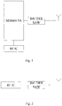
- the specific implementation circuit is shown in Fig. 1 and Fig. 2 .
- the defects of the above-mentioned designs are as the following description.
- the SAW package of the TRX part supporting the full-band B41 is 2016 size, and the SAW type of the DRX part is 1411 size. Both types are relatively large in size, and the size requirements of the layout are relatively high. With the integration of frequency bands of the projects is higher and higher, it is difficult to make it bigger, to place such a large device while ensuring good performance.
- the frequency band is wider, the price of a device of full-band is relatively higher. For example, the price of the TRX SAW device is above 0.34 US dollars, so that the overall price of the product designing will be higher.
- a purpose of the present disclosure is to provide a full-band radio frequency device and a communication terminal based on a frequency band B41.
- a main part and a diversity part are all realized by combining different frequency bands to realize the full-band communication in the frequency band B41. It may be advantageous for packaging the product, and the price of the device may be lower than the direct use of the full-band, so that the production cost may be saved.
- a full-band radio frequency device based on a frequency band B41 including a main part and a diversity part; wherein the main part includes a power amplifier module, a first filter module, and a duplex module; the power amplifier module is configured to perform amplification processing on an output signal; the first filter module is configured to perform filter processing on a transmitted or received signal in a first frequency band; the duplex module is configured to transmit or receive signals in a second frequency band; the diversity part includes a second filter module, and a third filter module; the second filter module is configured to perform filter processing on a received signal in a third frequency band; the third filter module is configured to perform filter processing on a received signal in a fourth frequency band; wherein the first frequency band and the second frequency band are combined into a full-band B41, and the third frequency band and the fourth frequency band are combined into a full-band B41.
- the full-band B41 is 2496MHz - 2690MHz; the first frequency band is 2580MHz - 2690MHz, the second frequency band is 2496MHz - 2580MHz; the third frequency band is 2496MHz - 2620MHz, and the fourth frequency band is 2620MHz - 2690MHz.
- the main part further includes a first antenna, and an antenna switch configured to control an operation state of the first antenna; the antenna switch is connected to the first antenna, the first filter module and the duplex module; and the diversity part further includes a second antenna, and a radio frequency switch configured to control an operation state of the second antenna; the radio frequency switch is connected to the second antenna, the second filter module, and a third filter module.
- the power amplifier module includes a multi-mode multi-frequency power amplifier and a filter unit; the filter unit performs filter processing on power supply voltage which is input to the multi-mode multi-frequency power amplifier; and the multi-mode multi-frequency power amplifier performs amplification processing on an output signal and outputs the output signal to the first filter module and the duplex module.
- the filter unit includes a first capacitor, a second capacitor, a third capacitor, a fourth capacitor, a fifth capacitor, and a sixth capacitor; one end of the first capacitor is connected to one end of the second capacitor, one end of the fourth capacitor, one end of the sixth capacitor, and a power supply end; the end of the second capacitor is further connected to one end of the third capacitor and a 28th pin of the multi-mode multi-frequency power amplifier; the end of the fourth capacitor is further connected to one end of the fifth capacitor and a 29th pin of the multi-mode multi-frequency power amplifier; the end of the sixth capacitor is further connected to a 30th pin of the multi-mode multi-frequency power amplifier; the other end of the first capacitor, the other end of the second capacitor, the other end of the third capacitor, the other end of the fourth capacitor, the other end of the fifth capacitor, and the other end of the sixth capacitor are grounded.
- the first filter module includes a filter, a seventh capacitor, an eighth capacitor, a ninth capacitor, a first inductor, and a second inductor; a 1st pin of the filter is connected to the multi-mode multi-frequency power amplifier and one end of the seventh capacitor through the first inductor, and the other end of the seventh capacitor is grounded; a 2nd pin of the filter is connected to one end of the eighth capacitor and one end of the second inductor, and the other end of the eighth capacitor is grounded; and the other end of the second inductor is grounded through the ninth capacitor.
- the duplex module includes a duplexer, a tenth capacitor, an eleventh capacitor, a twelfth capacitor, a thirteenth capacitor, a fourteenth capacitor, a third inductor, a fourth inductor, a fifth inductor, a sixth inductor, and a seventh inductor;
- a 3rd pin of the duplexer is connected to one end of the tenth capacitor and one end of the third inductor, and the other end of the tenth capacitor is grounded;
- the other end of the third inductor is connected to a 35th pin of the multi-mode multi-frequency power amplifier, and is further grounded through the eleventh capacitor;
- a 6th pin of the duplexer is connected to one end of the fifth inductor and one end of the twelfth capacitor, and the other end of the fifth inductor is grounded;
- the other end of the twelfth capacitor is grounded through the fourth inductor;
- a 1st pin of the duplexer is connected to one
- a type of the multi-mode multi-frequency power amplifier is AP7219M.
- a type of the duplexer is SAYEY2G53CA0F0A.
- the present disclosure further provides a communication terminal, which includes the full-band radio frequency device based on the frequency band B41.
- the full-band radio frequency device based on a frequency band B41 includes a main part and a diversity part; wherein the main part includes a power amplifier module, a first filter module, and a duplex module; the power amplifier module is configured to perform amplification processing on an output signal; the first filter module is configured to perform filter processing on a transmitted or received signal in a first frequency band; the duplex module is configured to transmit or receive signals in a second frequency band; the diversity part includes a second filter module, and a third filter module; the second filter module is configured to perform filter processing on a received signal in a third frequency band; the third filter module is configured to perform filter processing on a received signal in a fourth frequency band; wherein the first frequency band and the second frequency band are combined into a full-band B41, and the third frequency band and the fourth frequency band are combined into a full-band B41.
- a main part and a diversity part are all realized by combining different frequency bands to realize the full-band communication in the frequency band B41. It may be advantageous for packaging the product, and the price of the device may be lower than the direct use of the full-band, so that the production cost may be saved.
- the purpose of the present disclosure is to provide a full-band radio frequency device and a communication terminal based on a frequency band B41.
- a main part and a diversity part are all realized by combining different frequency bands to realize the full-band communication in the frequency band B41. It may be advantageous for packaging the product, and the price of the device may be lower than the direct use of the full-band, so that the production cost may be saved.
- the full-band radio frequency device based on a frequency band B41 may include a main part and a diversity part.
- the main part may include a power amplifier module 10, a first filter module 20, and a duplex module 30.
- the diversity part may include a second filter module 60 and a third filter module 70.
- the power amplifier module 10 may be connected to the first filter module 20 and the duplex module 30.
- the duplex module 30 and the power amplifier module 10 may be further connected to a radio frequency chip, i.e., a RF IC.
- the second filter module 60 and the third filter module 70 may be also connected to the radio frequency chip.
- the power amplifier module 10 may be configured to perform amplification processing on an output signal.
- the first filter module 20 may be configured to perform filter processing on a transmitted or received signal in a first frequency band.
- the duplex module 30 may be configured to transmit or receive signals in a second frequency band.
- the third filter module 70 may be configured to perform filter processing on a received signal in a fourth frequency band.
- the first frequency band and the second frequency band may be combined into a full-band B41, and the third frequency band and the fourth frequency band may be combined into a full-band B41.
- the main part may further include a first antenna 40 and an antenna switch 50 configured to control an operation state of the first antenna 40.
- the antenna switch 50 may be connected to the first antenna 40, the first filter module 20 and the duplex module 30.
- the diversity part may further include a second antenna 80 and a radio frequency switch 90 configured to control an operation state of the second antenna 80.
- the radio frequency switch 90 may be connected to the second antenna 80, the second filter module 60, and a third filter module 70.
- the main part and the diversity part may realize the full-band communication in the frequency band B41 by combining the devices of different frequency bands.
- the radio frequency chip may receive signals of the main part and the diversity part at the same time, to improve signal quality, sensitivity or achieve a special performance such as MIMO.
- the main part needs to include a function of transmitting signals, for a FDD (Frequency Division Duplex), the main part may use the duplex module 30 to transmit and receive signals simultaneously.
- the diversity part only needs to receive signals, so that the second filter module 60 and the third filter module 70 may be used to filter a received signal and transmit it to the radio frequency chip, to realize the transmission and reception of the radio frequency signal.
- the MT6169 of the MTK may be adopted to the radio frequency chip.
- Other radio frequency chips with same functions may also be adopted in other embodiments, it is not limited in the present disclosure.
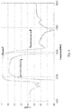
- the full-band B41 may be 2496MHz - 2690MHz. Since a TX (transmit) frequency band of a frequency band B7 and a low frequency band of the full-band B41 are basically overlapped, there is only a small part (2496MHz - 2500MHz, and 2570MHz - 2580MHz) not be overlapped. However, according to designs of duplexer, the bandwidth used is wider than the actual frequency band. According to actual testing results of the frequency band TX (transmit) of the frequency band B7, as shown in Fig. 6 , it may overlap 2496MHz - 2500MHz.
- the first frequency band may be 2580MHz - 2690MHz
- the second frequency band may be 2496MHz - 2580MHz
- the third frequency band may be 2496MHz - 2620MHz
- the fourth band may be 2620MHz - 2690MHz.
- the power amplifier module 10 may include a multi-mode multi-frequency power amplifier PA and a filter unit 101.
- the filter unit 101 may be connected to the multi-mode multi-frequency power amplifier PA.
- the multi-mode multi-frequency power amplifier PA may be further connected to a filter module and the duplex module 30.
- the filter unit 101 may perform filter processing on power supply voltage which is input to the multi-mode multi-frequency power amplifier PA.
- the multi-mode multi-frequency power amplifier PA may perform amplification processing on an output signal and output the output signal to the filter module and the duplex module 30.
- ripple voltage may be reduced by performing filter processing by the filter unit 101, on the power supply voltage which is input to the multi-mode multi-frequency power amplifier PA.
- a power amplifier of the type AP7219M may be adopted to the multi-mode multi-frequency power amplifier PA.
- other power amplifiers with same functions may be adopted, it is not limited in the present disclosure.
- the filter unit 101 may include a first capacitor C1, a second capacitor C2, a third capacitor C3, a fourth capacitor C4, a fifth capacitor C5, and a sixth capacitor C6.
- One end of the first capacitor C1 may be connected to one end of the second capacitor C2, one end of the fourth capacitor C4, one end of the sixth capacitor C6, and a first power supply end (a VBUS pin in this embodiment).
- the end of the second capacitor C2 may be further connected to one end of the third capacitor C3 and a 28th pin of the multi-mode multi-frequency power amplifier PA.
- the end of the fourth capacitor C4 may be further connected to one end of the fifth capacitor C5 and a 29th pin of the multi-mode multi-frequency power amplifier PA.
- the end of the sixth capacitor C6 may be further connected to a 30th pin of the multi-mode multi-frequency power amplifier PA.
- the other end of the first capacitor C1, the other end of the second capacitor C2, the other end of the third capacitor C3, the other end of the fourth capacitor C4, the other end of the fifth capacitor C5, and the other end of the sixth capacitor C6 may be grounded.
- the first filter module 20 may include a filter A1, a seventh capacitor C7, an eighth capacitor C8, a ninth capacitor C9, a first inductor L1, and a second inductor L2.
- a 1st pin of the filter A1 may be connected to the multi-mode multi-frequency power amplifier PA and one end of the seventh capacitor C7 through the first inductor L1, and the other end of the seventh capacitor C7 may be grounded.
- a 2nd pin of the filter A1 may be connected to one end of the eighth capacitor C8 and one end of the second inductor L2, and the other end of the eighth capacitor C8 may be grounded.
- the other end of the second inductor L2 may be grounded through the ninth capacitor C9, and further connected to the antenna switch 50.
- Capacitors and inductors in the first filter module 20 may be combined into a matching circuit to achieve impedance matching, specifically for adjusting a circuit, a device, and so on, to 50 ohm impedance.
- the filter A1 may be a B41 TRX SAW of a frequency band in 2580MHz - 2690MHz, i.e., a surface wave filter, and its type may be SAFFB2G35MAOFOA.
- other filters with same functions may be adopted, it is not limited in the present disclosure.
- the duplex module 30 may include a duplexer A2, a tenth capacitor C10, an eleventh capacitor C11, a twelfth capacitor C12, a thirteenth capacitor C13, a fourteenth capacitor C14, a third inductor L3, a fourth inductor L4, a fifth inductor L5, a sixth inductor L6, and a seventh inductor L7.
- a 3rd pin of the duplexer A2 may be connected to one end of the tenth capacitor C10 and one end of the third inductor L3, and the other end of the tenth capacitor C10 may be grounded.
- the other end of the third inductor L3 may be connected to a 35th pin of the multi-mode multi-frequency power amplifier PA, and may be further grounded through the eleventh capacitor C11.
- a 6th pin of the duplexer A2 may be connected to one end of the fifth inductor L5 and one end of the twelfth capacitor C12, and the other end of the fifth inductor L5 may be grounded.
- the other end of the twelfth capacitor C12 may be grounded through the fourth inductor L4, and further connected to the antenna switch 50.
- a 1st pin of the duplexer A2 may be connected to one end of the sixth inductor L6 and one end of the thirteenth capacitor C13, and the other end of the sixth inductor L6 may be connected to an 8th pin of the duplexer A2 and one end of the fourteenth capacitor C14.
- the other end of the thirteenth capacitor C13 may be connected to one end of the seventh inductor L7, and the other end of the seventh inductor L7 may be connected to the other end of the fourteenth capacitor C14.
- Capacitors and inductors in the duplex module 30 may be combined into a matching circuit to achieve impedance matching, specifically for adjusting a circuit, a device, and so on, to 50 ohm impedance.
- the duplexer A2 may be a type of SAYEY2G53CA0F0A, which may be configured to transmit and receive signals in a 2496MHz - 2580MHz band.
- a switch chip of a type AP6716M may be adopted to the antenna switch 50.
- other duplexers A2 and switch chips with same functions may be adopted, it is not limited in the present disclosure.
- a TRX SAW of the main part in the remaining frequency band B41 may be implemented in a 1411 package.
- the diversity part in the remaining frequency band B41 (2496MHz - 2610MHz) may be implemented in an 1109 package. Therefore, the package of the main part or the diversity part may be greatly reduced. A layout and a wiring may be improved. The device cost may be also greatly reduced. It may be also greatly advantageous for reducing the cost of the entire product.
- the full-band radio frequency device based on the frequency band B41 provided by the present disclosure may further include a transform matching module 110 configured to match impedance, and which may be connected to the multi-mode multi-frequency power amplifier PA.
- the transform matching module 110 may be a balun in the frequency band B41. Since a balanced circuit and an unbalanced circuit have different electrical characteristics when signals are transmitted and received, they cannot be easily connected to each other. The impedance matching may be performed by the transform matching module 110 to provide impedance conversion for the two different circuits, thereby a purpose of interference reducing may be achieved.
- the transform matching module 110 may include a converter A3, a fifteenth capacitor C15, a sixteenth capacitor C16, and an eighth inductor L8.
- One end of the fifteenth capacitor C15 may be connected to a 2nd pin of the converter A3.
- One end of the sixteenth capacitor C16 may be connected to a 6th pin of the converter A3.
- the other end of the fifteenth capacitor C15 and the other end of the sixteenth capacitor C16 may be grounded.
- a 5th Pin of the converter A3 may be connected to a 42th pin of the multi-mode multi-frequency power amplifier PA.
- a 3rd pin of the converter A3 may be a signal receiving input terminal in the frequency band B41 (i.e., a B41_RX_BLN_IN terminal), which may be also grounded through the eighth inductor L8.
- the present disclosure further provides a communication terminal, which may include the above-mentioned full-band radio frequency device based on the frequency band B41.
- a communication terminal which may include the above-mentioned full-band radio frequency device based on the frequency band B41.
- the full-band radio frequency device based on the frequency band B41 has been described above in detail, therefore no additional description is given herein.
- the full-band radio frequency device based on the frequency band B41 includes the main part and the diversity part; wherein the main part includes the power amplifier module, the first filter module, and the duplex module; the power amplifier module is configured to perform amplification processing on the output signal; the first filter module is configured to perform filter processing on the transmitted or received signal in the first frequency band; the duplex module is configured to transmit or receive signals in the second frequency band; the diversity part includes the second filter module, and the third filter module; the second filter module is configured to perform filter processing on the received signal in the third frequency band; the third filter module is configured to perform filter processing on the received signal in the fourth frequency band; wherein the first frequency band and the second frequency band are combined into the full-band B41, and the third frequency band and the fourth frequency band are combined into the full-band B41.
- the main part and the diversity part realize the full-band communication in the frequency band B41 by combining different frequency bands. It may be advantageous for packaging
Landscapes
- Engineering & Computer Science (AREA)
- Computer Networks & Wireless Communication (AREA)
- Signal Processing (AREA)
- Amplifiers (AREA)
- Transmitters (AREA)
- Transceivers (AREA)
- Radio Transmission System (AREA)
Abstract
Description
- The described embodiments relate to a communication technology, and more particularly, to a full-band radio frequency device based on a frequency band B41, and a communication terminal.
- Currently, as for the market is becoming wider and wider, requirements of the frequency band B41 become wider and wider, and the bandwidth of 2555MHz - 2655MHz (megahertz) is not limited to be used in the Chinese market. In order to make the same product not only to be used in the Chinese market, but also to be used in the frequency band B41 to be met in other regions such as Japan and United States, a design of the full-band B41 (2496MHz - 2690MHz) is required. In the previous designs, the main part uses the TRX SAW (transmitting and receiving filter) of the full-band B41, and the diversity part is uses the DRX SAW (receiving filter) of the full-band B41. The specific implementation circuit is shown in
Fig. 1 and Fig. 2 . - The defects of the above-mentioned designs are as the following description. (1) The SAW package of the TRX part supporting the full-band B41 is 2016 size, and the SAW type of the DRX part is 1411 size. Both types are relatively large in size, and the size requirements of the layout are relatively high. With the integration of frequency bands of the projects is higher and higher, it is difficult to make it bigger, to place such a large device while ensuring good performance. (2) Since the frequency band is wider, the price of a device of full-band is relatively higher. For example, the price of the TRX SAW device is above 0.34 US dollars, so that the overall price of the product designing will be higher.
- Therefore, the related art has yet to be improved.
- In view of the above-mentioned deficiencies of the related art, a purpose of the present disclosure is to provide a full-band radio frequency device and a communication terminal based on a frequency band B41. A main part and a diversity part are all realized by combining different frequency bands to realize the full-band communication in the frequency band B41. It may be advantageous for packaging the product, and the price of the device may be lower than the direct use of the full-band, so that the production cost may be saved.
- In order to achieve the above-mentioned purpose, the present disclosure adopts the following technical solutions.
- A full-band radio frequency device based on a frequency band B41, including a main part and a diversity part; wherein the main part includes a power amplifier module, a first filter module, and a duplex module; the power amplifier module is configured to perform amplification processing on an output signal; the first filter module is configured to perform filter processing on a transmitted or received signal in a first frequency band; the duplex module is configured to transmit or receive signals in a second frequency band; the diversity part includes a second filter module, and a third filter module; the second filter module is configured to perform filter processing on a received signal in a third frequency band; the third filter module is configured to perform filter processing on a received signal in a fourth frequency band; wherein the first frequency band and the second frequency band are combined into a full-band B41, and the third frequency band and the fourth frequency band are combined into a full-band B41.
- In the full-band radio frequency device based on the frequency band B41, the full-band B41 is 2496MHz - 2690MHz; the first frequency band is 2580MHz - 2690MHz, the second frequency band is 2496MHz - 2580MHz; the third frequency band is 2496MHz - 2620MHz, and the fourth frequency band is 2620MHz - 2690MHz.
- In the full-band radio frequency device based on the frequency band B41, the main part further includes a first antenna, and an antenna switch configured to control an operation state of the first antenna; the antenna switch is connected to the first antenna, the first filter module and the duplex module; and the diversity part further includes a second antenna, and a radio frequency switch configured to control an operation state of the second antenna; the radio frequency switch is connected to the second antenna, the second filter module, and a third filter module.
- In the full-band radio frequency device based on the frequency band B41, the power amplifier module includes a multi-mode multi-frequency power amplifier and a filter unit; the filter unit performs filter processing on power supply voltage which is input to the multi-mode multi-frequency power amplifier; and the multi-mode multi-frequency power amplifier performs amplification processing on an output signal and outputs the output signal to the first filter module and the duplex module.
- In the full-band radio frequency device based on the frequency band B41, the filter unit includes a first capacitor, a second capacitor, a third capacitor, a fourth capacitor, a fifth capacitor, and a sixth capacitor; one end of the first capacitor is connected to one end of the second capacitor, one end of the fourth capacitor, one end of the sixth capacitor, and a power supply end; the end of the second capacitor is further connected to one end of the third capacitor and a 28th pin of the multi-mode multi-frequency power amplifier; the end of the fourth capacitor is further connected to one end of the fifth capacitor and a 29th pin of the multi-mode multi-frequency power amplifier; the end of the sixth capacitor is further connected to a 30th pin of the multi-mode multi-frequency power amplifier; the other end of the first capacitor, the other end of the second capacitor, the other end of the third capacitor, the other end of the fourth capacitor, the other end of the fifth capacitor, and the other end of the sixth capacitor are grounded.
- In the full-band radio frequency device based on the frequency band B41, the first filter module includes a filter, a seventh capacitor, an eighth capacitor, a ninth capacitor, a first inductor, and a second inductor; a 1st pin of the filter is connected to the multi-mode multi-frequency power amplifier and one end of the seventh capacitor through the first inductor, and the other end of the seventh capacitor is grounded; a 2nd pin of the filter is connected to one end of the eighth capacitor and one end of the second inductor, and the other end of the eighth capacitor is grounded; and the other end of the second inductor is grounded through the ninth capacitor.
- In the full-band radio frequency device based on the frequency band B41, the duplex module includes a duplexer, a tenth capacitor, an eleventh capacitor, a twelfth capacitor, a thirteenth capacitor, a fourteenth capacitor, a third inductor, a fourth inductor, a fifth inductor, a sixth inductor, and a seventh inductor; a 3rd pin of the duplexer is connected to one end of the tenth capacitor and one end of the third inductor, and the other end of the tenth capacitor is grounded; the other end of the third inductor is connected to a 35th pin of the multi-mode multi-frequency power amplifier, and is further grounded through the eleventh capacitor; a 6th pin of the duplexer is connected to one end of the fifth inductor and one end of the twelfth capacitor, and the other end of the fifth inductor is grounded; the other end of the twelfth capacitor is grounded through the fourth inductor; a 1st pin of the duplexer is connected to one end of the sixth inductor and one end of the thirteenth capacitor, and the other end of the sixth inductor is connected to an 8th pin of the duplexer and one end of the fourteenth capacitor; and the other end of the thirteenth capacitor is connected to one end of the seventh inductor, and the other end of the seventh inductor is connected to the other end of the fourteenth capacitor.
- In the full-band radio frequency device based on the frequency band B41, a type of the multi-mode multi-frequency power amplifier is AP7219M.
- In the full-band radio frequency device based on the frequency band B41, a type of the duplexer is SAYEY2G53CA0F0A.
- The present disclosure further provides a communication terminal, which includes the full-band radio frequency device based on the frequency band B41.
- Compared to the related art, the full-band radio frequency device based on a frequency band B41 provided by the present disclosure, includes a main part and a diversity part; wherein the main part includes a power amplifier module, a first filter module, and a duplex module; the power amplifier module is configured to perform amplification processing on an output signal; the first filter module is configured to perform filter processing on a transmitted or received signal in a first frequency band; the duplex module is configured to transmit or receive signals in a second frequency band; the diversity part includes a second filter module, and a third filter module; the second filter module is configured to perform filter processing on a received signal in a third frequency band; the third filter module is configured to perform filter processing on a received signal in a fourth frequency band; wherein the first frequency band and the second frequency band are combined into a full-band B41, and the third frequency band and the fourth frequency band are combined into a full-band B41. A main part and a diversity part are all realized by combining different frequency bands to realize the full-band communication in the frequency band B41. It may be advantageous for packaging the product, and the price of the device may be lower than the direct use of the full-band, so that the production cost may be saved.
-
-
Fig. 1 is a structural block diagram of a main part of a radio frequency device based on a frequency band B41 in the related art. -
Fig. 2 is a structural block diagram of a diversity part of a radio frequency device based on a frequency band B41 in the related art. -
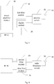
Fig. 3 is a structural block diagram of a main part of a radio frequency device based on a frequency band B41 in the present disclosure. -
Fig. 4 is a structural block diagram of a diversity part of a radio frequency device based on a frequency band B41 in the present disclosure. -
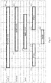
Fig. 5 is a distribution diagram of a full-band B41 and a frequency band B7 in a preferred embodiment of a radio frequency device based on a frequency band B41 in the present disclosure. -
Fig. 6 is a simulation test curve diagram of a TX band in a B7 duplexer in a preferred embodiment of a radio frequency device based on a frequency band B41 in the present disclosure. -
Fig. 7 is a circuit diagram of a power amplifier module, a first filter module, and a duplex module in a radio frequency device based on a frequency band B41 in the present disclosure. - In view of the disadvantages of the over-sized and high cost of the full-band communication projects in the frequency band B41 in the related art, the purpose of the present disclosure is to provide a full-band radio frequency device and a communication terminal based on a frequency band B41. A main part and a diversity part are all realized by combining different frequency bands to realize the full-band communication in the frequency band B41. It may be advantageous for packaging the product, and the price of the device may be lower than the direct use of the full-band, so that the production cost may be saved.
- The present disclosure will be further described in detail below with reference to the drawings and embodiments. It is understood that the specific embodiments described herein are merely illustrative of the disclosure and are not intended to limit the disclosure.
- Referring to
Fig. 3 and Fig. 4 , the full-band radio frequency device based on a frequency band B41 provided by the present disclosure, may include a main part and a diversity part. The main part may include apower amplifier module 10, afirst filter module 20, and aduplex module 30. The diversity part may include asecond filter module 60 and athird filter module 70. Thepower amplifier module 10 may be connected to thefirst filter module 20 and theduplex module 30. Theduplex module 30 and thepower amplifier module 10 may be further connected to a radio frequency chip, i.e., a RF IC. Thesecond filter module 60 and thethird filter module 70 may be also connected to the radio frequency chip. Thepower amplifier module 10 may be configured to perform amplification processing on an output signal. Thefirst filter module 20 may be configured to perform filter processing on a transmitted or received signal in a first frequency band. Theduplex module 30 may be configured to transmit or receive signals in a second frequency band. Thethird filter module 70 may be configured to perform filter processing on a received signal in a fourth frequency band. In addition, the first frequency band and the second frequency band may be combined into a full-band B41, and the third frequency band and the fourth frequency band may be combined into a full-band B41. - Further, the main part may further include a
first antenna 40 and anantenna switch 50 configured to control an operation state of thefirst antenna 40. Theantenna switch 50 may be connected to thefirst antenna 40, thefirst filter module 20 and theduplex module 30. The diversity part may further include asecond antenna 80 and aradio frequency switch 90 configured to control an operation state of thesecond antenna 80. Theradio frequency switch 90 may be connected to thesecond antenna 80, thesecond filter module 60, and athird filter module 70. When the antenna switch 50 and theradio frequency switch 90 are turned on, thefirst antenna 40 and thesecond antenna 80 may start to operate, to receive an external signal and transmit a signal to outside. - The main part and the diversity part may realize the full-band communication in the frequency band B41 by combining the devices of different frequency bands. When the radio frequency chip works, it may receive signals of the main part and the diversity part at the same time, to improve signal quality, sensitivity or achieve a special performance such as MIMO. Since the main part needs to include a function of transmitting signals, for a FDD (Frequency Division Duplex), the main part may use the
duplex module 30 to transmit and receive signals simultaneously. The diversity part only needs to receive signals, so that thesecond filter module 60 and thethird filter module 70 may be used to filter a received signal and transmit it to the radio frequency chip, to realize the transmission and reception of the radio frequency signal. In this embodiment, the MT6169 of the MTK may be adopted to the radio frequency chip. Other radio frequency chips with same functions may also be adopted in other embodiments, it is not limited in the present disclosure. - Referring to
Fig. 5 andFig. 6 , the full-band B41 may be 2496MHz - 2690MHz. Since a TX (transmit) frequency band of a frequency band B7 and a low frequency band of the full-band B41 are basically overlapped, there is only a small part (2496MHz - 2500MHz, and 2570MHz - 2580MHz) not be overlapped. However, according to designs of duplexer, the bandwidth used is wider than the actual frequency band. According to actual testing results of the frequency band TX (transmit) of the frequency band B7, as shown inFig. 6 , it may overlap 2496MHz - 2500MHz. Further, a frequency band RX (receive) of the frequency band B7 and a high frequency of the full-band B41 are fully reused. Therefore, based on the above-mentioned relationship, in a preferred embodiment of the present disclosure, the first frequency band may be 2580MHz - 2690MHz, the second frequency band may be 2496MHz - 2580MHz, the third frequency band may be 2496MHz - 2620MHz, and the fourth band may be 2620MHz - 2690MHz. By combining the devices of different frequency bands, the main part and the diversity part may realize the full-band communication in the frequency band B41. Compared with a device of the full-band, the cost may be greatly reduced, and the package size may be reduced. It may be advantageous for improving product integration. - Specifically, referring to
Fig. 7 , thepower amplifier module 10 may include a multi-mode multi-frequency power amplifier PA and afilter unit 101. Thefilter unit 101 may be connected to the multi-mode multi-frequency power amplifier PA. The multi-mode multi-frequency power amplifier PA may be further connected to a filter module and theduplex module 30. Thefilter unit 101 may perform filter processing on power supply voltage which is input to the multi-mode multi-frequency power amplifier PA. The multi-mode multi-frequency power amplifier PA may perform amplification processing on an output signal and output the output signal to the filter module and theduplex module 30. In the present disclosure, ripple voltage may be reduced by performing filter processing by thefilter unit 101, on the power supply voltage which is input to the multi-mode multi-frequency power amplifier PA. In this embodiment, a power amplifier of the type AP7219M may be adopted to the multi-mode multi-frequency power amplifier PA. In other embodiments, other power amplifiers with same functions may be adopted, it is not limited in the present disclosure. - Specifically, the
filter unit 101 may include a first capacitor C1, a second capacitor C2, a third capacitor C3, a fourth capacitor C4, a fifth capacitor C5, and a sixth capacitor C6. One end of the first capacitor C1 may be connected to one end of the second capacitor C2, one end of the fourth capacitor C4, one end of the sixth capacitor C6, and a first power supply end (a VBUS pin in this embodiment). The end of the second capacitor C2 may be further connected to one end of the third capacitor C3 and a 28th pin of the multi-mode multi-frequency power amplifier PA. The end of the fourth capacitor C4 may be further connected to one end of the fifth capacitor C5 and a 29th pin of the multi-mode multi-frequency power amplifier PA. The end of the sixth capacitor C6 may be further connected to a 30th pin of the multi-mode multi-frequency power amplifier PA. The other end of the first capacitor C1, the other end of the second capacitor C2, the other end of the third capacitor C3, the other end of the fourth capacitor C4, the other end of the fifth capacitor C5, and the other end of the sixth capacitor C6 may be grounded. - Further, the
first filter module 20 may include a filter A1, a seventh capacitor C7, an eighth capacitor C8, a ninth capacitor C9, a first inductor L1, and a second inductor L2. A 1st pin of the filter A1 may be connected to the multi-mode multi-frequency power amplifier PA and one end of the seventh capacitor C7 through the first inductor L1, and the other end of the seventh capacitor C7 may be grounded. A 2nd pin of the filter A1 may be connected to one end of the eighth capacitor C8 and one end of the second inductor L2, and the other end of the eighth capacitor C8 may be grounded. The other end of the second inductor L2 may be grounded through the ninth capacitor C9, and further connected to theantenna switch 50. Capacitors and inductors in thefirst filter module 20 may be combined into a matching circuit to achieve impedance matching, specifically for adjusting a circuit, a device, and so on, to 50 ohm impedance. In this embodiment, the filter A1 may be a B41 TRX SAW of a frequency band in 2580MHz - 2690MHz, i.e., a surface wave filter, and its type may be SAFFB2G35MAOFOA. In other embodiments, other filters with same functions may be adopted, it is not limited in the present disclosure. - Further, the
duplex module 30 may include a duplexer A2, a tenth capacitor C10, an eleventh capacitor C11, a twelfth capacitor C12, a thirteenth capacitor C13, a fourteenth capacitor C14, a third inductor L3, a fourth inductor L4, a fifth inductor L5, a sixth inductor L6, and a seventh inductor L7. A 3rd pin of the duplexer A2 may be connected to one end of the tenth capacitor C10 and one end of the third inductor L3, and the other end of the tenth capacitor C10 may be grounded. The other end of the third inductor L3 may be connected to a 35th pin of the multi-mode multi-frequency power amplifier PA, and may be further grounded through the eleventh capacitor C11. A 6th pin of the duplexer A2 may be connected to one end of the fifth inductor L5 and one end of the twelfth capacitor C12, and the other end of the fifth inductor L5 may be grounded. The other end of the twelfth capacitor C12 may be grounded through the fourth inductor L4, and further connected to theantenna switch 50. A 1st pin of the duplexer A2 may be connected to one end of the sixth inductor L6 and one end of the thirteenth capacitor C13, and the other end of the sixth inductor L6 may be connected to an 8th pin of the duplexer A2 and one end of the fourteenth capacitor C14. The other end of the thirteenth capacitor C13 may be connected to one end of the seventh inductor L7, and the other end of the seventh inductor L7 may be connected to the other end of the fourteenth capacitor C14. Capacitors and inductors in theduplex module 30 may be combined into a matching circuit to achieve impedance matching, specifically for adjusting a circuit, a device, and so on, to 50 ohm impedance. In this embodiment, the duplexer A2 may be a type of SAYEY2G53CA0F0A, which may be configured to transmit and receive signals in a 2496MHz - 2580MHz band. A switch chip of a type AP6716M may be adopted to theantenna switch 50. In other embodiments, other duplexers A2 and switch chips with same functions may be adopted, it is not limited in the present disclosure. - In the full-band radio frequency devices based on the frequency band B41 provided by the present disclosure, after removing a reused frequency band B7, a TRX SAW of the main part in the remaining frequency band B41 (2580MHz - 2690MHz) may be implemented in a 1411 package. In the market, such mature devices that may be adopted to reduce package size and save new device development costs. In addition to the reused band B7, the diversity part in the remaining frequency band B41 (2496MHz - 2610MHz) may be implemented in an 1109 package. Therefore, the package of the main part or the diversity part may be greatly reduced. A layout and a wiring may be improved. The device cost may be also greatly reduced. It may be also greatly advantageous for reducing the cost of the entire product.
- Preferably, the full-band radio frequency device based on the frequency band B41 provided by the present disclosure, may further include a
transform matching module 110 configured to match impedance, and which may be connected to the multi-mode multi-frequency power amplifier PA. Referring toFig. 7 , in this embodiment, thetransform matching module 110 may be a balun in the frequency band B41. Since a balanced circuit and an unbalanced circuit have different electrical characteristics when signals are transmitted and received, they cannot be easily connected to each other. The impedance matching may be performed by thetransform matching module 110 to provide impedance conversion for the two different circuits, thereby a purpose of interference reducing may be achieved. Thetransform matching module 110 may include a converter A3, a fifteenth capacitor C15, a sixteenth capacitor C16, and an eighth inductor L8. One end of the fifteenth capacitor C15 may be connected to a 2nd pin of the converter A3. One end of the sixteenth capacitor C16 may be connected to a 6th pin of the converter A3. The other end of the fifteenth capacitor C15 and the other end of the sixteenth capacitor C16 may be grounded. A 5th Pin of the converter A3 may be connected to a 42th pin of the multi-mode multi-frequency power amplifier PA. A 3rd pin of the converter A3 may be a signal receiving input terminal in the frequency band B41 (i.e., a B41_RX_BLN_IN terminal), which may be also grounded through the eighth inductor L8. - Based on the above-mentioned full-band radio frequency device based on the frequency band B41, the present disclosure further provides a communication terminal, which may include the above-mentioned full-band radio frequency device based on the frequency band B41. The full-band radio frequency device based on the frequency band B41 has been described above in detail, therefore no additional description is given herein.
- In summary, in the full-band radio frequency device based on the frequency band B41 provided by the present disclosure, the full-band radio frequency device based on the frequency band B41 includes the main part and the diversity part; wherein the main part includes the power amplifier module, the first filter module, and the duplex module; the power amplifier module is configured to perform amplification processing on the output signal; the first filter module is configured to perform filter processing on the transmitted or received signal in the first frequency band; the duplex module is configured to transmit or receive signals in the second frequency band; the diversity part includes the second filter module, and the third filter module; the second filter module is configured to perform filter processing on the received signal in the third frequency band; the third filter module is configured to perform filter processing on the received signal in the fourth frequency band; wherein the first frequency band and the second frequency band are combined into the full-band B41, and the third frequency band and the fourth frequency band are combined into the full-band B41. The main part and the diversity part realize the full-band communication in the frequency band B41 by combining different frequency bands. It may be advantageous for packaging the product, and the price of the device may be lower than the direct use of the full-band, so that the production cost may be saved.
- It should be understood that, those skilled in the art may make equivalent substitutions or changes to the embodiments in the present disclosure, and all such changes or substitutions belong to the scope of the appended claims.
Claims (20)
- A full-band radio frequency device based on a frequency band B41, comprising a main part and a diversity part; wherein
the main part comprisesa power amplifier module,a first filter module,a duplex module,a first antenna, andan antenna switch configured to control an operation state of the first antenna;the power amplifier module is connected to the first filter module and the duplex module;
the duplex module and the power amplifier module are further connected to a radio frequency chip;
the antenna switch is connected to the first antenna, the first filter module and the duplex module;
the power amplifier module is configured to perform amplification processing on an output signal;
the first filter module is configured to perform filter processing on a transmitted or received signal in a first frequency band;
the duplex module is configured to transmit or receive signals in a second frequency band;
the diversity part comprisesa second filter module,a third filter module,a second antenna, anda radio frequency switch configured to control an operation state of the second antenna;the second filter module and the third filter module are connected to the radio frequency chip;
the radio frequency switch is connected to the second antenna, the second filter module, and a third filter module;
the second filter module is configured to perform filter processing on a received signal in a third frequency band;
the third filter module is configured to perform filter processing on a received signal in a fourth frequency band;
the first frequency band and the second frequency band are combined into a full-band B41, and the third frequency band and the fourth frequency band are combined into a full-band B41;
wherein the full-band B41 is 2496MHz - 2690MHz; the first frequency band is 2580MHz - 2690MHz, the second frequency band is 2496MHz - 2580MHz; the third frequency band is 2496MHz - 2620MHz, and the fourth frequency band is 2620MHz - 2690MHz. - The full-band radio frequency device based on the frequency band B41 according to claim 1, wherein
the power amplifier module comprises a multi-mode multi-frequency power amplifier and a filter unit; the filter unit performs filter processing on power supply voltage which is input to the multi-mode multi-frequency power amplifier; and the multi-mode multi-frequency power amplifier performs amplification processing on an output signal and outputs the output signal to the first filter module and the duplex module. - A full-band radio frequency device based on a frequency band B41, comprising a main part and a diversity part; wherein
the main part comprisesa power amplifier module,a first filter module, anda duplex module;the power amplifier module is configured to perform amplification processing on an output signal;
the first filter module is configured to perform filter processing on a transmitted or received signal in a first frequency band;
the duplex module is configured to transmit or receive signals in a second frequency band;
the diversity part comprisesa second filter module, anda third filter module;the second filter module is configured to perform filter processing on a received signal in a third frequency band;
the third filter module is configured to perform filter processing on a received signal in a fourth frequency band;
wherein the first frequency band and the second frequency band are combined into a full-band B41, and the third frequency band and the fourth frequency band are combined into a full-band B41. - The full-band radio frequency device based on the frequency band B41 according to claim 3, wherein
the full-band B41 is 2496MHz - 2690MHz; the first frequency band is 2580MHz - 2690MHz, the second frequency band is 2496MHz - 2580MHz; the third frequency band is 2496MHz - 2620MHz, and the fourth frequency band is 2620MHz - 2690MHz. - The full-band radio frequency device based on the frequency band B41 according to claim 3, wherein
the main part further comprisesa first antenna, andan antenna switch configured to control an operation state of the first antenna;the antenna switch is connected to the first antenna, the first filter module and the duplex module; and
the diversity part further comprisesa second antenna, anda radio frequency switch configured to control an operation state of the second antenna;the radio frequency switch is connected to the second antenna, the second filter module, and a third filter module. - The full-band radio frequency device based on the frequency band B41 according to claim 3, wherein
the power amplifier module comprises a multi-mode multi-frequency power amplifier and a filter unit; the filter unit performs filter processing on power supply voltage which is input to the multi-mode multi-frequency power amplifier; and the multi-mode multi-frequency power amplifier performs amplification processing on an output signal and outputs the output signal to the first filter module and the duplex module. - The full-band radio frequency device based on the frequency band B41 according to claim 6, wherein
the filter unit comprisesa first capacitor,a second capacitor,a third capacitor,a fourth capacitor,a fifth capacitor, anda sixth capacitor;one end of the first capacitor is connected to one end of the second capacitor, one end of the fourth capacitor, one end of the sixth capacitor, and a power supply end;
the end of the second capacitor is further connected to one end of the third capacitor and a 28th pin of the multi-mode multi-frequency power amplifier;
the end of the fourth capacitor is further connected to one end of the fifth capacitor and a 29th pin of the multi-mode multi-frequency power amplifier;
the end of the sixth capacitor is further connected to a 30th pin of the multi-mode multi-frequency power amplifier;
the other end of the first capacitor, the other end of the second capacitor, the other end of the third capacitor, the other end of the fourth capacitor, the other end of the fifth capacitor, and the other end of the sixth capacitor are grounded. - The full-band radio frequency device based on the frequency band B41 according to claim 7, wherein
the first filter module comprisesa filter,a seventh capacitor,an eighth capacitor,a ninth capacitor,a first inductor, anda second inductor;a 1st pin of the filter is connected to the multi-mode multi-frequency power amplifier and one end of the seventh capacitorthrough the first inductor, and the other end of the seventh capacitoris grounded;
a 2nd pin of the filter is connected to one end of the eighth capacitor and one end of the second inductor, and the other end of the eighth capacitor is grounded; and
the other end of the second inductor is grounded through the ninth capacitor. - The full-band radio frequency device based on the frequency band B41 according to claim 7, wherein
the duplex module comprisesa duplexer,a tenth capacitor,an eleventh capacitor,a twelfth capacitor,a thirteenth capacitor,a fourteenth capacitor,a third inductor,a fourth inductor,a fifth inductor,a sixth inductor, anda seventh inductor;a 3rd pin of the duplexer is connected to one end of the tenth capacitor and one end of the third inductor, and the other end of the tenth capacitor is grounded;
the other end of the third inductor is connected to a 35th pin of the multi-mode multi-frequency power amplifier, and is further grounded through the eleventh capacitor;
a 6th pin of the duplexer is connected to one end of the fifth inductor and one end of the twelfth capacitor, and the other end of the fifth inductor is grounded;
the other end of the twelfth capacitor is grounded through the fourth inductor;
a 1st pin of the duplexer is connected to one end of the sixth inductor and one end of the thirteenth capacitor, and the other end of the sixth inductor is connected to an 8th pin of the duplexer and one end of the fourteenth capacitor; and
the other end of the thirteenth capacitor is connected to one end of the seventh inductor, and the other end of the seventh inductor is connected to the other end of the fourteenth capacitor. - The full-band radio frequency device based on the frequency band B41 according to claim 6, wherein
a type of the multi-mode multi-frequency power amplifier is AP7219M. - The full-band radio frequency device based on the frequency band B41 according to claim 9, wherein
a type of the duplexer is SAYEY2G53CA0F0A. - A communication terminal comprising a full-band radio frequency device based on a frequency band B41 having a main part and a diversity part; wherein
the main part comprisesa power amplifier module,a first filter module, anda duplex module;the power amplifier module is configured to perform amplification processing on an output signal;
the first filter module is configured to perform filter processing on a transmitted or received signal in a first frequency band;
the duplex module is configured to transmit or receive signals in a second frequency band;
the diversity part comprisesa second filter module, anda third filter module;the second filter module is configured to perform filter processing on a received signal in a third frequency band;
the third filter module is configured to perform filter processing on a received signal in a fourth frequency band;
wherein the first frequency band and the second frequency band are combined into a full-band B41, and the third frequency band and the fourth frequency band are combined into a full-band B41. - The communication terminal according to claim 12, wherein
the full-band B41 is 2496MHz - 2690MHz; the first frequency band is 2580MHz - 2690MHz, the second frequency band is 2496MHz - 2580MHz; the third frequency band is 2496MHz - 2620MHz, and the fourth frequency band is 2620MHz - 2690MHz. - The communication terminal according to claim 12, wherein
the main part further comprisesa first antenna, andan antenna switch configured to control an operation state of the first antenna;the antenna switch is connected to the first antenna, the first filter module and the duplex module; and
the diversity part further comprisesa second antenna, anda radio frequency switch configured to control an operation state of the second antenna;the radio frequency switch is connected to the second antenna, the second filter module, and a third filter module. - The communication terminal according to claim 12, wherein
the power amplifier module comprises a multi-mode multi-frequency power amplifier and a filter unit; the filter unit performs filter processing on power supply voltage which is input to the multi-mode multi-frequency power amplifier; and the multi-mode multi-frequency power amplifier performs amplification processing on an output signal and outputs the output signal to the first filter module and the duplex module. - The communication terminal according to claim 15, wherein
the filter unit comprisesa first capacitor,a second capacitor,a third capacitor,a fourth capacitor,a fifth capacitor, anda sixth capacitor;one end of the first capacitor is connected to one end of the second capacitor, one end of the fourth capacitor, one end of the sixth capacitor, and a power supply end;
the end of the second capacitor is further connected to one end of the third capacitor and a 28th pin of the multi-mode multi-frequency power amplifier;
the end of the fourth capacitor is further connected to one end of the fifth capacitor and a 29th pin of the multi-mode multi-frequency power amplifier;
the end of the sixth capacitor is further connected to a 30th pin of the multi-mode multi-frequency power amplifier;
the other end of the first capacitor, the other end of the second capacitor, the other end of the third capacitor, the other end of the fourth capacitor, the other end of the fifth capacitor, and the other end of the sixth capacitor are grounded. - The communication terminal according to claim 16, wherein
the first filter module comprisesa filter,a seventh capacitor,an eighth capacitor,a ninth capacitor,a first inductor, anda second inductor;a 1st pin of the filter is connected to the multi-mode multi-frequency power amplifier and one end of the seventh capacitor through the first inductor, and the other end of the seventh capacitoris grounded;
a 2nd pin of the filter is connected to one end of the eighth capacitor and one end of the second inductor, and the other end of the eighth capacitor is grounded; and
the other end of the second inductor is grounded through the ninth capacitor. - The communication terminal according to claim 16, wherein
the duplex module comprisesa duplexer,a tenth capacitor,an eleventh capacitor,a twelfth capacitor,a thirteenth capacitor,a fourteenth capacitor,a third inductor,a fourth inductor,a fifth inductor,a sixth inductor, anda seventh inductor;a 3rd pin of the duplexer is connected to one end of the tenth capacitor and one end of the third inductor, and the other end of the tenth capacitor is grounded;
the other end of the third inductor is connected to a 35th pin of the multi-mode multi-frequency power amplifier, and is further grounded through the eleventh capacitor;
a 6th pin of the duplexer is connected to one end of the fifth inductor and one end of the twelfth capacitor, and the other end of the fifth inductor is grounded;
the other end of the twelfth capacitor is grounded through the fourth inductor;
a 1st pin of the duplexer is connected to one end of the sixth inductor and one end of the thirteenth capacitor, and the other end of the sixth inductor is connected to an 8th pin of the duplexer and one end of the fourteenth capacitor; and
the other end of the thirteenth capacitor is connected to one end of the seventh inductor, and the other end of the seventh inductor is connected to the other end of the fourteenth capacitor. - The communication terminal according to claim 15, wherein
a type of the multi-mode multi-frequency power amplifier is AP7219M. - The communication terminal according to claim 18, wherein
a type of the duplexer is SAYEY2G53CA0F0A.
Applications Claiming Priority (2)
| Application Number | Priority Date | Filing Date | Title |
|---|---|---|---|
| CN201710601313.6A CN107171676B (en) | 2017-07-21 | 2017-07-21 | Full-band radio frequency device and communication terminal based on B41 frequency channel |
| PCT/CN2018/096684 WO2019015693A1 (en) | 2017-07-21 | 2018-07-23 | B41-based full-band radio frequency device and communication terminal |
Publications (3)
| Publication Number | Publication Date |
|---|---|
| EP3657685A1 true EP3657685A1 (en) | 2020-05-27 |
| EP3657685A4 EP3657685A4 (en) | 2020-08-05 |
| EP3657685B1 EP3657685B1 (en) | 2022-03-16 |
Family
ID=59818090
Family Applications (1)
| Application Number | Title | Priority Date | Filing Date |
|---|---|---|---|
| EP18834645.6A Active EP3657685B1 (en) | 2017-07-21 | 2018-07-23 | B41-based full-band radio frequency device and communication terminal |
Country Status (4)
| Country | Link |
|---|---|
| US (1) | US11251816B2 (en) |
| EP (1) | EP3657685B1 (en) |
| CN (1) | CN107171676B (en) |
| WO (1) | WO2019015693A1 (en) |
Families Citing this family (4)
| Publication number | Priority date | Publication date | Assignee | Title |
|---|---|---|---|---|
| CN107171676B (en) * | 2017-07-21 | 2020-01-14 | 惠州Tcl移动通信有限公司 | Full-band radio frequency device and communication terminal based on B41 frequency channel |
| CN109004949B (en) * | 2018-11-01 | 2020-03-27 | Oppo(重庆)智能科技有限公司 | LTE communication circuit and LTE communication terminal |
| JP2020167445A (en) * | 2019-03-28 | 2020-10-08 | 株式会社村田製作所 | Front-end circuit and communication device |
| CN111030618B (en) * | 2019-12-24 | 2024-11-15 | 中交星宇科技有限公司 | A dual-frequency positioning circuit and a dual-frequency positioning device |
Family Cites Families (9)
| Publication number | Priority date | Publication date | Assignee | Title |
|---|---|---|---|---|
| US9935760B2 (en) * | 2013-04-16 | 2018-04-03 | Qorvo Us, Inc. | Tunable filter for LTE bands |
| US9768941B2 (en) * | 2013-04-29 | 2017-09-19 | Skyworks Solutions, Inc. | Duplexer architectures and methods for enabling additional signal path |
| US20150372702A1 (en) * | 2014-06-24 | 2015-12-24 | Qualcomm Incorporated | Filters for a frequency band |
| CN105553499B (en) * | 2015-10-29 | 2019-03-08 | 东莞酷派软件技术有限公司 | A radio frequency front end of a mobile terminal and a mobile terminal |
| CN105656610B (en) * | 2015-12-30 | 2019-02-01 | 宇龙计算机通信科技(深圳)有限公司 | Realize the radio circuit and terminal of carrier wave polymerization |
| CN205945728U (en) * | 2016-08-11 | 2017-02-08 | 惠州Tcl移动通信有限公司 | Mobile device and communication device thereof |
| CN106921405A (en) * | 2017-02-28 | 2017-07-04 | 维沃移动通信有限公司 | A kind of radio frequency front-end device |
| CN107171676B (en) * | 2017-07-21 | 2020-01-14 | 惠州Tcl移动通信有限公司 | Full-band radio frequency device and communication terminal based on B41 frequency channel |
| US11121736B2 (en) * | 2019-04-26 | 2021-09-14 | Qorvo Us, Inc. | Radio frequency circuit supporting carrier aggregation |
-
2017
- 2017-07-21 CN CN201710601313.6A patent/CN107171676B/en active Active
-
2018
- 2018-07-23 WO PCT/CN2018/096684 patent/WO2019015693A1/en not_active Ceased
- 2018-07-23 EP EP18834645.6A patent/EP3657685B1/en active Active
-
2019
- 2019-12-13 US US16/713,021 patent/US11251816B2/en active Active
Also Published As
| Publication number | Publication date |
|---|---|
| WO2019015693A1 (en) | 2019-01-24 |
| US20200145029A1 (en) | 2020-05-07 |
| EP3657685A4 (en) | 2020-08-05 |
| US11251816B2 (en) | 2022-02-15 |
| CN107171676A (en) | 2017-09-15 |
| EP3657685B1 (en) | 2022-03-16 |
| CN107171676B (en) | 2020-01-14 |
Similar Documents
| Publication | Publication Date | Title |
|---|---|---|
| US11251816B2 (en) | Full-band radio frequency device and communication terminal based on frequency band B41 | |
| JP5237414B2 (en) | Terminal apparatus for simultaneously transmitting signals to which different wireless communication schemes are applied through a plurality of frequency bands | |
| CN108110423B (en) | Antenna tuning circuit, antenna device and mobile terminal | |
| CN103337717B (en) | Antenna impedance matching device, semi-conductor chip and antenna impedance matching method | |
| WO2021143877A1 (en) | Radio frequency circuit and electronic device | |
| CN108134202B (en) | Antenna tuning circuit and mobile terminal | |
| US20140273887A1 (en) | Tunable ila and dila matching for simultaneous high and low band operation | |
| US20150188225A1 (en) | Antenna assembly and wireless communication device using the same | |
| CN111327344A (en) | Radio frequency system and electronic equipment | |
| CN102394667B (en) | Mobile terminal and GPS and 3G single-antenna realizing device | |
| CN109547038B (en) | Inter-band uplink carrier aggregation radio frequency circuit, antenna device and electronic equipment | |
| CN108377151B (en) | A multi-mode multi-frequency wireless radio frequency front-end module, chip and communication terminal | |
| WO2013075404A1 (en) | Matching circuit, matching circuit network, and signal transceiver device | |
| CN105553499A (en) | Mobile terminal radio frequency front-end and mobile terminal | |
| CN101557237A (en) | Radio-frequency front-end transceiver and multi-mode mobile terminal | |
| CN116015318A (en) | A multi-band radio frequency front-end device, a multi-band receiver and a multi-band transmitter | |
| JP2016072951A (en) | Wireless communication device | |
| CN204156853U (en) | A kind of device for mating antenna and multi-frequency band radio-frequency transceiver module | |
| CN104577332A (en) | Full-closed loop automatic tuning control device and method for improving stray isolation degree between antennas | |
| CN106100652B (en) | Spurious suppression device and method | |
| CN203839510U (en) | A mobile phone and its antenna | |
| CN107659277A (en) | A kind of double-frequency broadband power amplifier matching circuit for GaN power devices | |
| EP4462690A1 (en) | Radio-frequency front-end circuit and electronic device | |
| CN101521519A (en) | Signal transmitting and receiving device for wireless communication device | |
| CN107493115A (en) | Communication RF front-end circuit and mobile terminal |
Legal Events
| Date | Code | Title | Description |
|---|---|---|---|
| STAA | Information on the status of an ep patent application or granted ep patent |
Free format text: STATUS: THE INTERNATIONAL PUBLICATION HAS BEEN MADE |
|
| PUAI | Public reference made under article 153(3) epc to a published international application that has entered the european phase |
Free format text: ORIGINAL CODE: 0009012 |
|
| STAA | Information on the status of an ep patent application or granted ep patent |
Free format text: STATUS: REQUEST FOR EXAMINATION WAS MADE |
|
| 17P | Request for examination filed |
Effective date: 20191216 |
|
| AK | Designated contracting states |
Kind code of ref document: A1 Designated state(s): AL AT BE BG CH CY CZ DE DK EE ES FI FR GB GR HR HU IE IS IT LI LT LU LV MC MK MT NL NO PL PT RO RS SE SI SK SM TR |
|
| AX | Request for extension of the european patent |
Extension state: BA ME |
|
| A4 | Supplementary search report drawn up and despatched |
Effective date: 20200703 |
|
| RIC1 | Information provided on ipc code assigned before grant |
Ipc: H04B 1/00 20060101AFI20200629BHEP |
|
| DAV | Request for validation of the european patent (deleted) | ||
| DAX | Request for extension of the european patent (deleted) | ||
| GRAP | Despatch of communication of intention to grant a patent |
Free format text: ORIGINAL CODE: EPIDOSNIGR1 |
|
| STAA | Information on the status of an ep patent application or granted ep patent |
Free format text: STATUS: GRANT OF PATENT IS INTENDED |
|
| INTG | Intention to grant announced |
Effective date: 20211115 |
|
| GRAS | Grant fee paid |
Free format text: ORIGINAL CODE: EPIDOSNIGR3 |
|
| GRAA | (expected) grant |
Free format text: ORIGINAL CODE: 0009210 |
|
| STAA | Information on the status of an ep patent application or granted ep patent |
Free format text: STATUS: THE PATENT HAS BEEN GRANTED |
|
| AK | Designated contracting states |
Kind code of ref document: B1 Designated state(s): AL AT BE BG CH CY CZ DE DK EE ES FI FR GB GR HR HU IE IS IT LI LT LU LV MC MK MT NL NO PL PT RO RS SE SI SK SM TR |
|
| REG | Reference to a national code |
Ref country code: GB Ref legal event code: FG4D |
|
| REG | Reference to a national code |
Ref country code: CH Ref legal event code: EP |
|
| REG | Reference to a national code |
Ref country code: DE Ref legal event code: R096 Ref document number: 602018032457 Country of ref document: DE |
|
| REG | Reference to a national code |
Ref country code: IE Ref legal event code: FG4D |
|
| REG | Reference to a national code |
Ref country code: AT Ref legal event code: REF Ref document number: 1476605 Country of ref document: AT Kind code of ref document: T Effective date: 20220415 |
|
| REG | Reference to a national code |
Ref country code: LT Ref legal event code: MG9D |
|
| REG | Reference to a national code |
Ref country code: NL Ref legal event code: MP Effective date: 20220316 |
|
| PG25 | Lapsed in a contracting state [announced via postgrant information from national office to epo] |
Ref country code: SE Free format text: LAPSE BECAUSE OF FAILURE TO SUBMIT A TRANSLATION OF THE DESCRIPTION OR TO PAY THE FEE WITHIN THE PRESCRIBED TIME-LIMIT Effective date: 20220316 Ref country code: RS Free format text: LAPSE BECAUSE OF FAILURE TO SUBMIT A TRANSLATION OF THE DESCRIPTION OR TO PAY THE FEE WITHIN THE PRESCRIBED TIME-LIMIT Effective date: 20220316 Ref country code: NO Free format text: LAPSE BECAUSE OF FAILURE TO SUBMIT A TRANSLATION OF THE DESCRIPTION OR TO PAY THE FEE WITHIN THE PRESCRIBED TIME-LIMIT Effective date: 20220616 Ref country code: LT Free format text: LAPSE BECAUSE OF FAILURE TO SUBMIT A TRANSLATION OF THE DESCRIPTION OR TO PAY THE FEE WITHIN THE PRESCRIBED TIME-LIMIT Effective date: 20220316 Ref country code: HR Free format text: LAPSE BECAUSE OF FAILURE TO SUBMIT A TRANSLATION OF THE DESCRIPTION OR TO PAY THE FEE WITHIN THE PRESCRIBED TIME-LIMIT Effective date: 20220316 Ref country code: BG Free format text: LAPSE BECAUSE OF FAILURE TO SUBMIT A TRANSLATION OF THE DESCRIPTION OR TO PAY THE FEE WITHIN THE PRESCRIBED TIME-LIMIT Effective date: 20220616 |
|
| REG | Reference to a national code |
Ref country code: AT Ref legal event code: MK05 Ref document number: 1476605 Country of ref document: AT Kind code of ref document: T Effective date: 20220316 |
|
| PG25 | Lapsed in a contracting state [announced via postgrant information from national office to epo] |
Ref country code: LV Free format text: LAPSE BECAUSE OF FAILURE TO SUBMIT A TRANSLATION OF THE DESCRIPTION OR TO PAY THE FEE WITHIN THE PRESCRIBED TIME-LIMIT Effective date: 20220316 Ref country code: GR Free format text: LAPSE BECAUSE OF FAILURE TO SUBMIT A TRANSLATION OF THE DESCRIPTION OR TO PAY THE FEE WITHIN THE PRESCRIBED TIME-LIMIT Effective date: 20220617 Ref country code: FI Free format text: LAPSE BECAUSE OF FAILURE TO SUBMIT A TRANSLATION OF THE DESCRIPTION OR TO PAY THE FEE WITHIN THE PRESCRIBED TIME-LIMIT Effective date: 20220316 |
|
| PG25 | Lapsed in a contracting state [announced via postgrant information from national office to epo] |
Ref country code: NL Free format text: LAPSE BECAUSE OF FAILURE TO SUBMIT A TRANSLATION OF THE DESCRIPTION OR TO PAY THE FEE WITHIN THE PRESCRIBED TIME-LIMIT Effective date: 20220316 |
|
| PG25 | Lapsed in a contracting state [announced via postgrant information from national office to epo] |
Ref country code: SM Free format text: LAPSE BECAUSE OF FAILURE TO SUBMIT A TRANSLATION OF THE DESCRIPTION OR TO PAY THE FEE WITHIN THE PRESCRIBED TIME-LIMIT Effective date: 20220316 Ref country code: SK Free format text: LAPSE BECAUSE OF FAILURE TO SUBMIT A TRANSLATION OF THE DESCRIPTION OR TO PAY THE FEE WITHIN THE PRESCRIBED TIME-LIMIT Effective date: 20220316 Ref country code: RO Free format text: LAPSE BECAUSE OF FAILURE TO SUBMIT A TRANSLATION OF THE DESCRIPTION OR TO PAY THE FEE WITHIN THE PRESCRIBED TIME-LIMIT Effective date: 20220316 Ref country code: PT Free format text: LAPSE BECAUSE OF FAILURE TO SUBMIT A TRANSLATION OF THE DESCRIPTION OR TO PAY THE FEE WITHIN THE PRESCRIBED TIME-LIMIT Effective date: 20220718 Ref country code: ES Free format text: LAPSE BECAUSE OF FAILURE TO SUBMIT A TRANSLATION OF THE DESCRIPTION OR TO PAY THE FEE WITHIN THE PRESCRIBED TIME-LIMIT Effective date: 20220316 Ref country code: EE Free format text: LAPSE BECAUSE OF FAILURE TO SUBMIT A TRANSLATION OF THE DESCRIPTION OR TO PAY THE FEE WITHIN THE PRESCRIBED TIME-LIMIT Effective date: 20220316 Ref country code: CZ Free format text: LAPSE BECAUSE OF FAILURE TO SUBMIT A TRANSLATION OF THE DESCRIPTION OR TO PAY THE FEE WITHIN THE PRESCRIBED TIME-LIMIT Effective date: 20220316 Ref country code: AT Free format text: LAPSE BECAUSE OF FAILURE TO SUBMIT A TRANSLATION OF THE DESCRIPTION OR TO PAY THE FEE WITHIN THE PRESCRIBED TIME-LIMIT Effective date: 20220316 |
|
| PG25 | Lapsed in a contracting state [announced via postgrant information from national office to epo] |
Ref country code: PL Free format text: LAPSE BECAUSE OF FAILURE TO SUBMIT A TRANSLATION OF THE DESCRIPTION OR TO PAY THE FEE WITHIN THE PRESCRIBED TIME-LIMIT Effective date: 20220316 Ref country code: IS Free format text: LAPSE BECAUSE OF FAILURE TO SUBMIT A TRANSLATION OF THE DESCRIPTION OR TO PAY THE FEE WITHIN THE PRESCRIBED TIME-LIMIT Effective date: 20220716 Ref country code: AL Free format text: LAPSE BECAUSE OF FAILURE TO SUBMIT A TRANSLATION OF THE DESCRIPTION OR TO PAY THE FEE WITHIN THE PRESCRIBED TIME-LIMIT Effective date: 20220316 |
|
| REG | Reference to a national code |
Ref country code: DE Ref legal event code: R097 Ref document number: 602018032457 Country of ref document: DE |
|
| PLBE | No opposition filed within time limit |
Free format text: ORIGINAL CODE: 0009261 |
|
| STAA | Information on the status of an ep patent application or granted ep patent |
Free format text: STATUS: NO OPPOSITION FILED WITHIN TIME LIMIT |
|
| PG25 | Lapsed in a contracting state [announced via postgrant information from national office to epo] |
Ref country code: DK Free format text: LAPSE BECAUSE OF FAILURE TO SUBMIT A TRANSLATION OF THE DESCRIPTION OR TO PAY THE FEE WITHIN THE PRESCRIBED TIME-LIMIT Effective date: 20220316 |
|
| 26N | No opposition filed |
Effective date: 20221219 |
|
| PG25 | Lapsed in a contracting state [announced via postgrant information from national office to epo] |
Ref country code: SI Free format text: LAPSE BECAUSE OF FAILURE TO SUBMIT A TRANSLATION OF THE DESCRIPTION OR TO PAY THE FEE WITHIN THE PRESCRIBED TIME-LIMIT Effective date: 20220316 Ref country code: MC Free format text: LAPSE BECAUSE OF FAILURE TO SUBMIT A TRANSLATION OF THE DESCRIPTION OR TO PAY THE FEE WITHIN THE PRESCRIBED TIME-LIMIT Effective date: 20220316 |
|
| REG | Reference to a national code |
Ref country code: CH Ref legal event code: PL |
|
| REG | Reference to a national code |
Ref country code: BE Ref legal event code: MM Effective date: 20220731 |
|
| PG25 | Lapsed in a contracting state [announced via postgrant information from national office to epo] |
Ref country code: LU Free format text: LAPSE BECAUSE OF NON-PAYMENT OF DUE FEES Effective date: 20220723 Ref country code: LI Free format text: LAPSE BECAUSE OF NON-PAYMENT OF DUE FEES Effective date: 20220731 Ref country code: CH Free format text: LAPSE BECAUSE OF NON-PAYMENT OF DUE FEES Effective date: 20220731 |
|
| PG25 | Lapsed in a contracting state [announced via postgrant information from national office to epo] |
Ref country code: BE Free format text: LAPSE BECAUSE OF NON-PAYMENT OF DUE FEES Effective date: 20220731 |
|
| P01 | Opt-out of the competence of the unified patent court (upc) registered |
Effective date: 20230530 |
|
| PG25 | Lapsed in a contracting state [announced via postgrant information from national office to epo] |
Ref country code: IT Free format text: LAPSE BECAUSE OF FAILURE TO SUBMIT A TRANSLATION OF THE DESCRIPTION OR TO PAY THE FEE WITHIN THE PRESCRIBED TIME-LIMIT Effective date: 20220316 Ref country code: IE Free format text: LAPSE BECAUSE OF NON-PAYMENT OF DUE FEES Effective date: 20220723 |
|
| PG25 | Lapsed in a contracting state [announced via postgrant information from national office to epo] |
Ref country code: MK Free format text: LAPSE BECAUSE OF FAILURE TO SUBMIT A TRANSLATION OF THE DESCRIPTION OR TO PAY THE FEE WITHIN THE PRESCRIBED TIME-LIMIT Effective date: 20220316 Ref country code: CY Free format text: LAPSE BECAUSE OF FAILURE TO SUBMIT A TRANSLATION OF THE DESCRIPTION OR TO PAY THE FEE WITHIN THE PRESCRIBED TIME-LIMIT Effective date: 20220316 |
|
| PG25 | Lapsed in a contracting state [announced via postgrant information from national office to epo] |
Ref country code: HU Free format text: LAPSE BECAUSE OF FAILURE TO SUBMIT A TRANSLATION OF THE DESCRIPTION OR TO PAY THE FEE WITHIN THE PRESCRIBED TIME-LIMIT; INVALID AB INITIO Effective date: 20180723 |
|
| PG25 | Lapsed in a contracting state [announced via postgrant information from national office to epo] |
Ref country code: TR Free format text: LAPSE BECAUSE OF FAILURE TO SUBMIT A TRANSLATION OF THE DESCRIPTION OR TO PAY THE FEE WITHIN THE PRESCRIBED TIME-LIMIT Effective date: 20220316 |
|
| PG25 | Lapsed in a contracting state [announced via postgrant information from national office to epo] |
Ref country code: MT Free format text: LAPSE BECAUSE OF FAILURE TO SUBMIT A TRANSLATION OF THE DESCRIPTION OR TO PAY THE FEE WITHIN THE PRESCRIBED TIME-LIMIT Effective date: 20220316 |
|
| PGFP | Annual fee paid to national office [announced via postgrant information from national office to epo] |
Ref country code: DE Payment date: 20250722 Year of fee payment: 8 |
|
| PGFP | Annual fee paid to national office [announced via postgrant information from national office to epo] |
Ref country code: GB Payment date: 20250722 Year of fee payment: 8 |
|
| PGFP | Annual fee paid to national office [announced via postgrant information from national office to epo] |
Ref country code: FR Payment date: 20250725 Year of fee payment: 8 |